
Submitted:
28 September 2023
Posted:
03 October 2023
You are already at the latest version
Abstract
Electro-optic modulator (EOM) is one of the key devices of high-speed optical fiber communication system and ultra-wideband microwave photonic system. Silicon-organic hybrid (SOH) integration platform combines the advantages of silicon photonics and organic materials, providing a high electro-optic effect and compact structure for photonic integrated devices. In this paper we present a SOH integrated EOM with comprehensive investigation of EOM structure design, silicon waveguide fabrication with Slot structure, on-chip poling of organic electro-optic material, and characterization of EO modulation response. The SOH integrated EOM is measured with 3dB-bandwidth of over 50 GHz and half-wave voltage length product of 0.26 V·cm. Furthermore, we demonstrate a microwave photonics phase shifter by using the fabricated SOH integrated dual parallel Mach-Zehnder modulator. The phase shift range of 410 degree is completed from 8 GHz to 26 GHz with a power consumption of less than 38 mW.
Keywords:
Electro-optic modulator
; silicon photonics
; silicon-organic hybrid
; Mach-Zehnder modulator
; slot waveguide
1. Introduction
Integration is an inevitable trend in future photonics technology development, which can greatly reduce the size, weight and power consumption (SWaP) of the system. As a key component in highly integrated optoelectronic systems, the electro-optic modulators (EOMs) have great potential for applications in fields such as optical communications [1,2] and microwave photonics [3,4,5,6,7,8,9]. The high-performance EOMs should simultaneously have large electro-optic (EO) response bandwidth, small half-wave voltage Vπ and short device length L. The common EOMs can be divided into three categories according to the materials: LiNbO3 (LN), Si and EO polymer. LN modulators are the most general and mature EO modulators in current fiber-optical communication system [10]. And the recent developed thin-film LN modulators can be integrated with silicon photonic platform showing the wide bandwidth and low half-wave voltage [11,12,13,14]. Integrated EOMs based on silicon achieving EO modulation function by free-carrier dispersion effect have a good potential because of strongly optical field confinement of silicon waveguide and complementary metal–oxide–semiconductor (CMOS) compatibility [15,16,17,18]. With the rapid development of silicon photonics, it has become a major commercial photonics platform for integrated system. Besides Si and LiNbO3, another potential material for EOMs is the EO polymer. Through the optimal design of molecule structure in organic EO material, the ultra-high EO coefficient can be achieved, which attracts the increasing attention in past years [19,20,21].
Silicon-organic hybrid (SOH) platform combines the advantages of high integration of silicon photonics and strong linear electro-optic effect of organic material. SOH integrated modulators can achieve the large bandwidth, low half-wave voltage, and short device length at the same time. With the rapid development of fabrication craft, the performance of SOH integrated EOMs are being enhanced greatly. In 2009, J. Leuthold’s group verified the feasibility of SOH modulators for the first time [22]. Christian Koos’s group has done a lot of researches on SOH modulator design, fabrication [23,24] and applications [25,26]. They carried out a detailed theoretical study of SOH modulator based on Slot waveguides and greatly expanded the bandwidth of modulator in experiments. In addition, Shiyoshi Yokoyama’s group investigated the thermal stability of SOH modulators for harsh environment [27,28]. The performance of SOH modulators is becoming increasingly superior through the in-depth exploration of SOH modulators by researchers.
In this paper we carry out a comprehensive and in-depth study on SOH EOM. The EOM structure design, Slot silicon waveguide fabrication, on-chip organic electro-optic material poling, and the characterization of EO modulation response are investigated comprehensively. The performance of the fabricated MZM is measured and characterized with 3dB-bandwidth of over 50 GHz and half-wave voltage length product of 0.26 V·cm. Furthermore, we have developed a SOH integrated dual parallel Mach-Zehnder modulator for application in microwave photonics signal processing systems. We have optimized the phase shifting scheme for microwave photonics and performed functional testing and analysis of the phase shifter. The phase shift voltage is controlled in the 0-14V range, achieving a high frequency flatness phase shift from X-band to K-band (8 GHz-26 GHz) of more than 410° with a power consumption of less than 38 mW. The measured results demonstrate the feasibility of the developed electro-optic modulator for application in microwave photonics signal processing.
2. Modulator Design and Device Fabrication
The schematic structure of the SOH Mach-Zehnder modulator (MZM) is shown in Figure 1. The MZM comprises two SOH phase shifters driven by coplanar waveguide electrodes. Silicon Slot waveguide is formed by two silicon rails with a narrow slot filled by EO organic material, as shown in Figure 1b. The EO polymer is guest-host doped system and prepared by the Institute of Physics and Chemistry of the Chinese Academy of Sciences [29]. The chromophores are dissolved followed by doping in to the polymer matrix functioning as guest. Host material is polymethyl methacrylate (PMMA). The molecular structure of CLD chromophore is shown in Figure 1c. The electron giving ability of the donor in the chromophore and the electron absorbing ability of the acceptor are very strong, so it has a good molecular first-order hyperpolarizability (microscopic electro-optical activity). The acceptor part of CLD chromophore molecule is to introduce additional groups in the furan ring of tricyanofuran (TCF), which increases the electron absorbing ability of TCF receptor, which is beneficial to improve its EO properties, but also increases the difficulty of synthesis. At the same time, the middle conjugated π-electron bridge uses isophorone with high electron transport capacity, which makes the performance of the whole structure very excellent. The absorption loss of EO polymer at 1550 nm is about 3.6 dB/cm. The refractive index of the polymer film was measured as 1.72 using Metricon Prism Coupler Model 2010/M (Metricon, Piscataway, NJ, USA).
The dielectric constants of Si (12.0) and organic polymer (2.9) differ significantly at 1550 nm. And the dielectric constant discontinuity on sidewall of Slot waveguide makes optical field confined within the Slot strongly. For the modulation electric field, the electric field can be well applied on the two sides of the Slot waveguide due to the doping of the silicon slab as well. In other words, the optical field and the modulation electric field can be confined within the same Slot region to obtain high modulation efficiency.
The structure of the Slot waveguide and the distribution of the optical and electric field modes in the Slot structure are given in Figure 2. As can be seen in Figure 2b, the optical field distribution of the Slot waveguide is different from that of the general strip waveguide. The field distribution in Strip waveguides is Gauss mode and in Slot waveguides is non-Gauss mode, which will induce large coupling loss when the two waveguides are connected directly. Therefore, the Strip-to-Slot mode converter is designed to reduce the mode conversion loss from Gauss-like mode to non-Gauss-like mode. The structure and the transmission optical field of the Strip-to-Slot mode conversion are shown in Figure 3. By optimizing the design of the Strip-to-Slot mode converter, the coupling efficiency can reach 99.31%.
Figure 4 shows the main nine steps of fabrication process of SOH integrated EOM. The modulators were fabricated by the Institute of Microelectronics of the Chinese Academy of Sciences. Silicon-on-insulator wafers were used, with 220-nm silicon on top of 3μm silicon dioxide. The silicon waveguides were processed using deep ultraviolet lithography followed by etching. The width of Slot is 150nm and the width of silicon rails beside Slot is 250nm. In order to direct the electric field from the upper metal electrode to both sides of the Slot waveguide, silicon needs to be doped. We used graded doping to avoid significant optical losses due to doping. The silicon near Slot is n-doped with concentration of 3×1016 cm-3, while the concentration further away is 1×1020 cm-3. In step (7) and (8), we first used a dry etched of 1.2μm and then a wet etched for 3 mins to remove the silicon oxide from the Slot waveguide without damaging the rest of the structure.
After completing the preparation of waveguide and electrode based on steps (1)-(8) in Figure 4, the 8-inch wafer made with modulator structures is shown in Figure 5, with a single block size of 12mm×16mm.
A rotational coating method is used to fill the EO organic polymer into the Slot uniformly and sufficiently as shown in Figure 6. First, the polymer and chromophores are dissolved in organic solvent at a certain mass percentage; The chip to be spin-coated is placed in the spin-coater, and then a certain amount of polymer solution is added dropwise to the device surface; The chip with EO polymer on the surface is spun in the spin-coater for a period of time to form a thin and uniform film on the device surface; After spin-coating, the chip is placed on a heating plate at 70 ℃ (Bakon BK946S) for 15 minutes to remove most of the solvent and release the stress from the polymer chain segments. The chip is then placed in a vacuum drying oven for 12 hours with a vacuum of less than -0.09 MPa and a temperature of 60 ℃ for ensuring that the organic solvent is completely evaporated and will not affect the subsequent operations.
Figure 7 shows the SEM images of the Slot waveguide cross-sectional before and after spin-coating polymer. As can be seen from Figure 7b, the overall EO polymer filling in the Slot waveguide is complete, uniform, sufficient and with no bubbles. It can also be seen that in the process of Slot structure etching, the SiO2 under the Slot waveguide is hollowed out, which has little effect on the final performance of the device with simulation analysis.
As initially the orientation of chromophores in the Slot waveguide follows thermodynamic statistical rules, and it implies that there is no macroscopic EO response. To achieve a macroscopic EO effect in the material, it is necessary to align the chromophores in the EO polymer material. The most common method used for this purpose is electric field poling [30], which is divided into corona poling and contact poling. The on-chip poling of EO polymers is implemented directly by using the electrodes of the modulator and its electric field poling mechanism is similar to that of contact poling. As shown in Figure 8, the electric field poling mechanism of EO polymers can be described as follows: At the glass transition temperature (Tg), the polymer transitions from a glassy state to a high elasticity state, and at this point, the binding force between the chromophores and the polymer is relatively weak, allowing the chromophores to rotate freely within a certain range in the polymer. Therefore, under the external electric field, the dipole moment of the chromophore tends to align with the electric field direction, causing the chromophores to rotate and maintain their alignment for a period of time. When this rotation becomes stable, the temperature of the polymer is cooled to room temperature, and the polymer returns to a state of strong binding force. The chromophores in the polymer are thus unable to rotate freely after the external electric field is removed, resulting in their maintained alignment. Through the above series of operations, the polarized polymer achieves a macroscopic EO effect.
For on-chip poling of EO polymers, a DC probe is connected to the modulator electrode PAD after the chip is fixed by a vacuum adsorption plate, and a DC high-voltage power supply (TD2200P5-150) is used to provide an adjustable DC voltage of 0-5 kV to the chip. A source meter (Keithley 2602) is used to monitor the current through the polymer in the slot during poling. The temperature on chip is controlled by a temperature controller (Lightwave LDT-5525B) during poling, and the chip can be rapidly heated and cooled by a semiconductor cooler.
Figure 9a shows a schematic diagram of the electric field in the cross-section of the modulating region during device polarization and operation. The electrodes used for polarization are the same as those used for modulation, which simplify device structure and reduce preparation difficulty. The black (dotted line) and red (solid line) arrows in the figure respectively indicate the direction of the polarization electric field and the modulation electric field in the cross-section of the modulating region, and the directions of the modulation electric field and polarization electric field in the two arms are the same and opposite, respectively. This makes push-pull operation possible and improves the modulation efficiency and reduces power consumption of the device. Figure 9b shows the voltage and temperature curves on the chip during the final optimized polarization process. During the polarization process, the polarization voltage is set to 20 V until the temperature reaches 82 °C (glass transition temperature Tg). After the temperature reaches Tg , the polarization voltage gradually increases to 40 V. About three minutes later, while maintaining the voltage at 40 V, the temperature on the chip rapidly drops to room temperature, and finally the polarization voltage is withdrawn to complete the polarization. The entire polarization process takes about seven minutes.
3. Device Characterization
The S-parameters of electrode directly affect its final bandwidth and power consumption of EO modulator. When measuring its electrical performance such as S-parameters, it can be considered as electrical two-port network and analyzed directly by an electrical vector network analyzer (VNA, Keysight, N5247B). In order to accurately measure the performance parameters of the modulator, the reference plane of the VNA should be calibrated to both ends of the electrode before the measurement. The calibration method used is the Short-Open-Load-Through (SOLT) method, which is one of the most dominant calibration methods for on-chip testing [31].
The measured S-parameters of electrode are shown in Figure 10. The S21 curve decreases by approximately 1 dB over the range of 60 GHz, while the modulator’s S11 is less than -10 dB, indicating low transmission loss of the modulator electrodes and small reflected signals. According to Equation (1) and (2), the characteristic impedance of electrode Z0 and propagation constant γ can be calculated by S-parameters [32].
where Zref is the reference impedance of the measurement system, which is 50 ohms. α is the attenuation factor, NRF is the effective refractive index of the microwave signal, and c is the speed of light in a vacuum.
The characteristic impedance and refractive index curves of the coplanar waveguide electrode are shown in Figure 11. The characteristic impedance of the electrode is around 45 ohms, while the effective refractive index of the microwave is around 4.7.
For high-performance EO modulators, the frequency response bandwidth is the most important factor determining for signal transmission speed. The experimental setup shown in Figure 12a was used to test the RF response of the modulator chip, and the test results are shown in Figure 12b. It can be seen that the EO modulator with a 3-dB bandwidth of over 50 GHz, where the frequency response of the RF probes and PD has been removed.
The half-wave voltage length product VπL characterizes the modulating efficient of EOM for a specific wavelength of input light. The smaller VπL means that the lower power consumption and more compact device size. It is depended on:
where the wavelength λ of laser is 1550 nm, the refractive index of the polymer material n is 1.72, the width of Slot waveguide WSlot is 150 nm, the γ33 is in-device EO coefficient. Γ is the confinement factor of the optical field, defined as ratio between the optical power in the Slot waveguides and the total power propagating, as shown in Equation (5). The confinement factor Γ for the tested MZM was calculated to be approximately 14.2%.
The experimental setup for testing the half-wave voltage is shown in Figure 13a. The half-wave voltage measurement is performed by using the characteristic of the voltage of the triangle-wave that increases linearly with time, so we can easily read the half-wave voltage from the oscilloscope (RIGOL, DS1104) by comparing the input and output waveforms. Figure 13b shows that the measured half-wave voltage Vπ at 100 kHz is 5.12 V and the half-wave voltage length product VπL is 0.26 V·cm with the modulation length of 0.5 mm. According to (4), the in-device EO coefficient γ33 is calculated to be 63 pm/V which is about twice of that in LN.
To test the stability of the device modulation performance, three sample chips were tracked over a long period of time as shown in Figure 14. The half-wave voltage of the device rises to 1.4-1.8 times its initial value after more than 4000 hours, and the thermo-optical coefficient of the polymer material decreases to about 0.6-0.7 just after poling and remains stable. This indicates that the device still maintains a comparable modulation performance after being stored at room temperature for more than 4000 hours to meet the practical use requirements.
4. Microwave Phase Shifter Based on Dual-Parallel Mach-Zehnder Modulator
Due to the numerous benefits, including wide bandwidth, low losses, immunity to electromagnetic interferences, photonics RF phase shifter has been as important components of phased-arrayed beam-forming network and microwave photonic filters. We demonstrate a simple photonics RF phase shifter based on SOH Dual-Parallel Mach-Zehnder modulator (DP-MZM). The schematic diagram is shown in Figure 15.
DP-MZM is comprised of two MZMs that can input RF signal individually in parallel. And the optical phase between two sub-MZMs can be control by V3. The laser output optical carrier enters the DP-MZM and is divided into two equal power parts into two sub-MZMs (sub-MZM1 and sub-MZM2). Sub-MZM1 is loaded with RF signal and operates at the minimum point to achieve carrier suppression double sideband modulation. The carrier power in the output spectrum of Sub-MZM1 reaches minimum and the first-order sideband power reaches maximum, and the power magnitude of the carrier is determined by the extinction ratio of the modulator. The Sub-MZM2 is not loaded with RF signal and only provides optical carrier, working at the maximum point. Finally, the relative phase of between the two sidebands from Sub-MZM1 and carrier from Sub-MZM2 is adjusted by VDC3 and then combined to output. Then DP-MZM output signal is filtered by optical filters to remove the negative first-order optical sidebands from the spectral components and input to the photodetector. The photodetector transforms the signal into electric domain. Neglecting the higher-order components of the spectrum, the DP-MZM output signal can be expressed as follows when only the first-order optical sidebands are considered.
where A0 is the amplitude of the sub-MZM2 output optical carrier. k1-2 is the carrier suppression ratio, which represents the ratio of the residual carrier power when sub-MZM1 is operating at the minimum point and the maximum output optical power. It should be noted that the value of k1-2 is determined by the modulator extinction ratio. A1 is the amplitude of the positive and negative first-order sidebands when sub-MZM1 is operating at the minimum point. θ is the phase difference caused by the DC bias voltage V3 and the θ =π·(V3/Vπ3)2. Vπ3 is the DC voltage of for π phase shift.
Before entering the PD, the negative first-order sidebands need to be filtered out by using an optical bandpass filter. The power of the optical carrier is also reduced a little due to the restricted steepness of the optical bandpass filter, and the spectral components after the optical filter can be expressed as:
where k2-2 represents the power attenuation of the optical carrier after the filter, k3-2 is the power ratio of the negative first-order optical sidebands to the positive first-order optical sidebands. After the PD photoelectric conversion of the photocurrent from these spectral components beat frequency, ignoring the DC term as well as the multiplier term, the photocurrent can be expressed as:
We would like to have only cos(ωRFt+θ) in the PD output signal, If the negative first-order sidebands are completely filtered out and the sub-MZM1 does not output an optical carrier at all, the phase difference between the output microwave signal and the input microwave signal depends entirely on the phase difference θ between the two sub-MZMs. But there are other terms in the output signal due to the finite extinction ratio of the sub-MZM1. Also, the negative first-order sidebands cannot be completely filtered out, especially when the sidebands are closer to the carrier, which results in the presence of the correlation term in the output signal. The equation (8) is further simplified to:
where A3 and φ1 are:
The output microwave signal can eventually be expressed as:
where A and φ are:
The variations of the RF phase shift and the power with θ for different carrier suppression ratio k1-2 and sidebands suppression ratio k3-2 are calculated by Equation (12) as shown in Figure 16 and Figure 17. As can be seen from Figure 16, the phase shift of the RF signal basically presents a linear increase trend with the increase of phase difference θ, and the linearity of phase shift increase is better with the increase of carrier suppression ratio and sideband suppression ratio. Figure 17 shows the variation of RF signal power with phase difference. As can be seen from Figure 17, in the range of phase difference changes, the power variation of the RF signal presents periodic fluctuations. When the carrier suppression ratio is 40 dB (30 dB) and the sideband suppression ratio is 30 dB (40 dB) dB, the RF signal power variation fluctuation is only in the range of 0.6 dB.
In the experiments, the laser source (NKT Photonics K81-152-04) outputs an optical carrier with optical power of 9 dBm. The optical signal is adjusted by polarization controller and then couples through the waveguide grating into the modulator chip. VNA port 1 outputs microwave signal to sub-MZM1, which operates at the minimum bias point to obtain the carrier suppressed double sidebands modulated optical signal. The phase difference between sub-MZM1 and sub-MZM2 is adjusted by a thermo-optic electrode. Optical signal through the waveguide grating coupling out of the chip into the erbium-doped fiber amplifier (KEOSPSYS, CEFA-C-HG-SM-40-B130-FA-FA). The amplified signal is input to the optical bandpass filter (OPBF) to suppress the negative first-order sidebands and then input to the photodetector. The photodetector transforms the optical signal to electric signal and returns it to the port 2 of VNA. According to the S-parameters the VNA obtains the amplitude and phase shift of the RF signal.
In experiment, the sub-MZM1 is operating at minimum point and sub-MZM2 is operating the at maximum point. The optical bandpass filter is set to make lower sideband at the stopping band and the carrier and upper sideband at passing band. The output optical spectrum of DPMZM measured by optical spectrum analyzer (YOKOGAWA, AQ6370D) is shown in Figure 18a. The modulated optical signal after OBPF and the transmission spectrum of OBPF are shown in Figure 18b.
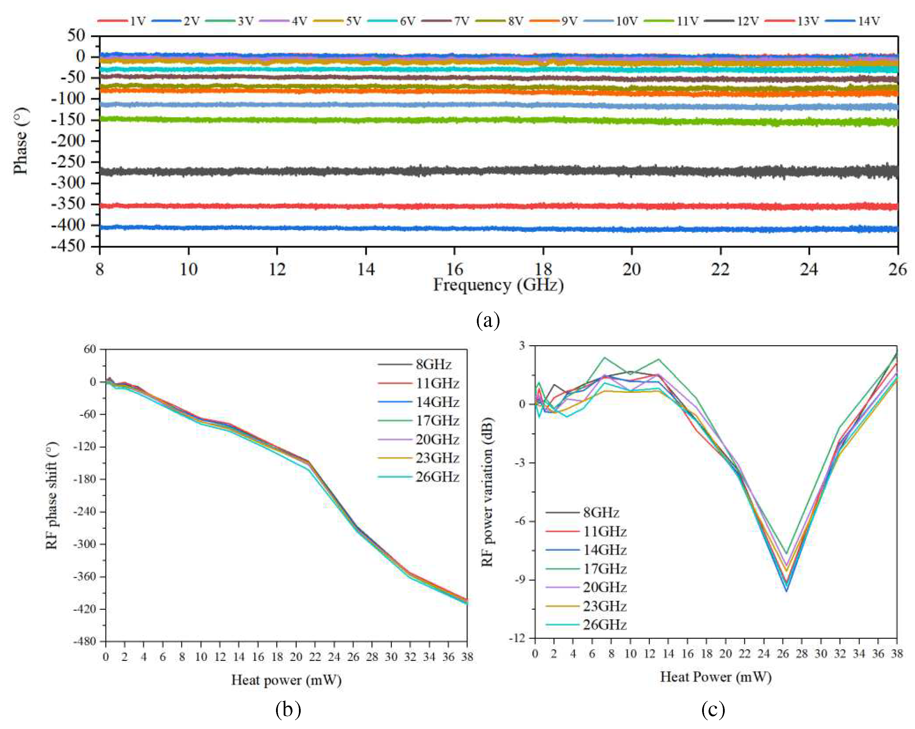
Figure 19a shows the tunable RF phase up to 410° over the frequency from 8 to 26 GHz. And the RF phase shift and power stability versus the heating power for different RF frequencies of 8-26 GHz are measured and shown in Figure 19b,c. The photonic RF phase shifter based on DP-MZM achieves a phase shift range of greater than 410° at a phase shift power of 38 mW and has a well in-band consistency. But the RF power has a variation during phase shift. From Figure 16 and Figure 17, it can be seen that the power variation is mainly due to the finite carrier suppression ratio. According to the theoretical analysis Figure 17, the carrier suppression ratio of sub-MZM1 can be presumed to be higher than 10 dB.
5. Conclusions
We designed and fabricated a SOH Mach-Zehnder modulator featuring an EO response 3dB-bandwidth of 50 GHz and half-wave voltage length product of 0.26 V·cm, by virtue of the high EO coefficient in device of γ33=63 pm/V. In addition, we investigated a photonic RF phase shifter based on the SOH dual parallel Mach-Zehnder modulator. The phase shift range of 410 degrees was achieved over the frequency band from 8 GHz to 26 GHz with a power consumption of less than 38 mW.
Author Contributions
Conceptualization, X. Han and Z. Chen; methodology, Z. Zhou and X. Han; validation, Z. Zhou, M. Chao, X. Su, X. Yang and Z. Wu; formal analysis, Z. Zhou and X. Su; Resources, Z. Chen, S. Bo, R. Liu and Z. Li; writing—original draft preparation, Z. Zhou; writing—review and editing, X. Han, and M. Chao. All authors have read and agreed to the published version of the manuscript.
Funding
This research was supported in part by National Natural Science Foundation of China (62075026, 61875028), Liao Ning Revitalization Talents Program (XLYC2002111), Program for Innovative Talents in Universities of Liaoning Province (LR2019017) and Fundamental Research Funds for the Central Universities (DUT22ZD202).
Data Availability Statement
Data underlying the results presented in this paper are not publicly available at this time but may be obtained from the authors upon reasonable request.
Conflicts of Interest
The authors declare no conflict of interest.
References
- Winzer, P.J.; Neilson, D.T.; Chraplyvy, A.R. Fiber-optic transmission and networking: the previous 20 and the next 20 year. Opt. Express 2018, 26, 24190. [Google Scholar] [CrossRef] [PubMed]
- Misra, A.; Preussler, S.; Singh, K.; Meier, J.; Schneider, T. Modulation format aggregation of Nyquist channels by spectral superposition with electro-optic modulators. In Proceedings of the Optical Fiber Communication Conference (OFC), San Diego, CA, USA, 06–10 March 2022. [Google Scholar]
- Yao, J.; Capmany, J. Microwave photonics. Sci. China Inf. Sci. 2022, 65, 314–335. [Google Scholar] [CrossRef]
- Li, J.; Yang, Si.; Chen, H.; Wang, X.; Chen, M.; Zou, W. Fully integrated hybrid microwave photonic receiver. Photonics Res. 2022, 10, 1472–1483. [Google Scholar] [CrossRef]
- Tao, Z.H.; Tao, Y.S.; Jin, M.; Qin, J.; Chen, R.X.; Shen, B.T.; Wu, Y.C.; Shu, H.W.; Yu, S.H.; Wang, X.J. Highly reconfigurable silicon integrated microwave photonic filter towards next-generation wireless communication. Photonics Res. 2023, 11, 682–694. [Google Scholar] [CrossRef]
- Guo, J.S.; Yu, L.W.; Xiang, H.T.; Zhao, Y.Q.; Liu, C.Y.; Dai, D.X. Realization of advanced passive silicon photonic devices with subwavelength grating structures developed by efficient inverse design. Advanced Photonics Nexus 2023, 2, 026005. [Google Scholar] [CrossRef]
- Park, D.H.; Pagán, V.R.; Luo, J.; Jen, A.K.Y.; Petruzzi, P.V. RF photonic down-conversion of a QPSK signal with a millimeter-wave coupled polymer phase modulator. In Proceedings of the Optics InfoBase Conference Papers; 2017, Waikoloa, HI, USA, 17–21 July 2017. [Google Scholar]
- Han, X.Y.; Su, X.X.; Chao, M.; Yang, X.D.; Wang, W.H.; Fu, S.L.; Du, Y.C.; Wu, Z.L.; Zhao, M.S. Integrated photonic RF self-interference cancellation on silicon platform for full-duplex communication. Photonics Res. 2023. [Google Scholar] [CrossRef]
- Marpaung, D.; Yao, J.; Capmany, J. Integrated microwave photonics. Nat. Photonics 2019, 13, 80–90. [Google Scholar] [CrossRef]
- Wooten, E.L.; Kissa, K.M.; Yi-Yan, A.; Murphy, E.J.; Lafaw, D.A.; Hallemeier, P.F.; Maack, D.; Attanasio, D.V.; Fritz, D.J.; McBrien, G.J.; et al. Review of lithium niobate modulators for fiber-optic communications systems. IEEE J. Sel. Top. Quantum Electron. 2000, 6, 69–82. [Google Scholar] [CrossRef]
- Weigel, P.O.; Zhao, J.; Fang, K.; Al-Rubaye, H.; Trotter, D.; Hood, D.; Mudrick, J.; Dallo, C.; Pomerene, A.T.; Starbuck, A.L.; et al. Bonded thin film lithium niobate modulator on a silicon photonics platform exceeding 100 GHz 3-dB electrical modulation bandwidth. Opt. Express 2018, 26, 23728. [Google Scholar] [CrossRef]
- Zhang, M.; Wang, C.; Kharel, P.; Zhu, D.; Lončar, M. Integrated lithium niobate electro-optic modulators: when performance meets scalability. Optica 2021, 8, 652. [Google Scholar] [CrossRef]
- Chen, G.; Li, N.; Ng, J.D.; Lin, H.L.; Zhou, Y.; Fu, Y.H.; Lee, L.Y.T.; Yu, Y.; Liu, A.Q.; Danner, A.J. Advances in lithium niobate photonics: development status and perspectives. Advanced Photonics 2022, 4, 034003. [Google Scholar] [CrossRef]
- Liu, X.; Xiong, B.; Sun, C.; Wang, J.; Hao, Z.; Wang, L.; Han, Y.; Li, H.; Yu, J.; Luo, Y. Wideband thin-film lithium niobate modulator with low half-wave-voltage length product. Chinese Opt. Lett. 2021, 19, 060016. [Google Scholar] [CrossRef]
- Rahim, A.; Hermans, A.; Wohlfeil, B.; Petousi, D.; Kuyken, B.; Van Thourhout, D.; Baets, R. Taking silicon photonics modulators to a higher performance level: state-of-the-art and a review of new technologies. Advanced Photonics 2021, 3, 024003. [Google Scholar] [CrossRef]
- Zhou, J.; Wang, J.; Zhu, L.; Zhang, Q. Silicon photonics for 100 Gbaud. J. Light. Technol. 2021, 39, 857–867. [Google Scholar] [CrossRef]
- Patel, D.; Ghosh, S.; Chagnon, M.; Samani, A.; Veerasubramanian, V.; Osman, M.; Plant, D.V. Design, analysis, and transmission system performance of a 41 GHz silicon photonic modulator. Opt. Express 2015, 23, 14263. [Google Scholar] [CrossRef]
- Han, C.; Jin, M.; Tao, Y.; Shen, B.; Shu, H.; Wang, X. Ultra-compact silicon modulator with 110 GHz bandwidth. In Proceedings of the Optical Fiber Communication Conferenc, San Diego, CA, USA, 6–10 March 2022. [Google Scholar]
- Lee, M.; Katz, H.E.; Erben, C.; Gill, D.M.; Gopalan, P.; Heber, J.D.; McGee, D.J. Broadband modulation of light by using an electro-optic polymer. Science. 2002, 298, 1401–1403. [Google Scholar] [CrossRef]
- Miura, H.; Qiu, F.; Spring, A.M.; Kashino, T.; Kikuchi, T.; Ozawa, M.; Nawata, H.; Odoi, K.; Yokoyama, S. High thermal stability 40 GHz electro-optic polymer modulators. Opt. Express 2017, 25, 28643. [Google Scholar] [CrossRef]
- Ullah, F.; Deng, N.; Qiu, F. Recent progress in electro-optic polymer for ultra-fast communication. PhotoniX 2021, 2, 1–18. [Google Scholar] [CrossRef]
- Koos, C.; Vorreau, P.; Vallaitis, T.; Dumon, P.; Bogaerts, W.; Baets, R.; Esembeson, B.; Biaggio, I.; Michinobu, T.; Diederich, F.; et al. All-optical high-speed signal processing with silicon-organic hybrid slot waveguides. Nat. Photonics 2009, 3, 216–219. [Google Scholar] [CrossRef]
- Zwickel, H.; Singer, S.; Kieninger, C.; Kutuvantavida, Y.; Muradyan, N.; Wahlbrink, T.; Yokoyama, S.; Randel, S.; Freude, W.; Koos, C. Verified equivalent-circuit model for slot-waveguide modulators. Opt. Express 2020, 28, 12951. [Google Scholar] [CrossRef]
- Ummethala, S.; Kemal, J.N.; Alam, A.S.; Lauermann, M.; Kuzmin, A.; Kutuvantavida, Y.; Nandam, S.H.; Hahn, L.; Elder, D.L.; Dalton, L.R.; et al. Hybrid electro-optic modulator combining silicon photonic slot waveguides with high-k radio-frequency slotlines. Optica 2021, 8, 511. [Google Scholar] [CrossRef]
- Wolf, S.; Zwickel, H.; Hartmann, W.; Lauermann, M.; Kutuvantavida, Y.; Kieninger, C.; Altenhain, L.; Schmid, R.; Luo, J.; Jen, A.K.Y.; et al. Silicon-organic hybrid (SOH) Mach-Zehnder modulators for 100 Gbit/s on-off keying. Sci. Rep. 2018, 8, 1–13. [Google Scholar] [CrossRef] [PubMed]
- Kieninger, C.; Kutuvantavida, Y.; Elder, D.L.; Wolf, S.; Zwickel, H.; Blaicher, M.; Kemal, J.N.; Lauermann, M.; Randel, S.; Freude, W.; et al. Ultra-high electro-optic activity demonstrated in a silicon-organic hybrid modulator. Optica 2018, 5, 739. [Google Scholar] [CrossRef]
- Yokoyama, S.; Lu, G.W.; Cheng, X.; Qiu, F. Long-term stable electro-optic polymer for hybrid integration. In Proceedings of the Optical Fiber Communication Conference, San Diego, CA, USA, 3–7 March 2019. [Google Scholar]
- Lu, G.W.; Hong, J.; Qiu, F.; Spring, A.M.; Kashino, T.; Oshima, J.; Ozawa, M. aki; Nawata, H.; Yokoyama, S. High-temperature-resistant silicon-polymer hybrid modulator operating at up to 200 Gbit/s for energy-efficient datacentres and harsh-environment applications. Nat. Commun. 2020, 11, 1–9. [Google Scholar]
- Bo, S.; Li, Y.; Liu, T.; Huo, F.; Xiao, H.; Zhang, H.; Chen, Z. Systematic study on the optimization of a bis (N, N-diethyl) aniline based NLO chromophore via a stronger electron acceptor, extended π-conjugation and isolation groups. J. Mater. Chem. C 2022, 10, 3343–3352. [Google Scholar] [CrossRef]
- Burland, D.M.; Miller, R.D.; Walsh, C.A. Second-order nonlinearity in poled-polymer systems. Chem. Rev. 1994, 94, 31–75. [Google Scholar] [CrossRef]
- Fregonese, S.; Deng, M.; De Matos, M.; Yadav, C.; Joly, S.; Plano, B.; Raya, C.; Ardouin, B.; Zimmer, T. Comparison of on-wafer TRL calibration to ISS SOLT calibration with open-short de-embedding up to 500 GHz. IEEE Trans. Terahertz Sci. Technol. 2019, 9, 89–97. [Google Scholar] [CrossRef]
- Eisenstadt, W.R.; Eo, Y. S-parameter-based IC interconnect transmission line characterization. IEEE Trans. Components, Hybrids, Manuf. Technol. 1992, 15, 483–490. [Google Scholar] [CrossRef]
Figure 1.
(a) Micrograph of the fabricated MZM; (b) 3D diagram of a silicon-organic hybrid MZM; (c) Molecular structure of EO organic material.
Figure 1.
(a) Micrograph of the fabricated MZM; (b) 3D diagram of a silicon-organic hybrid MZM; (c) Molecular structure of EO organic material.
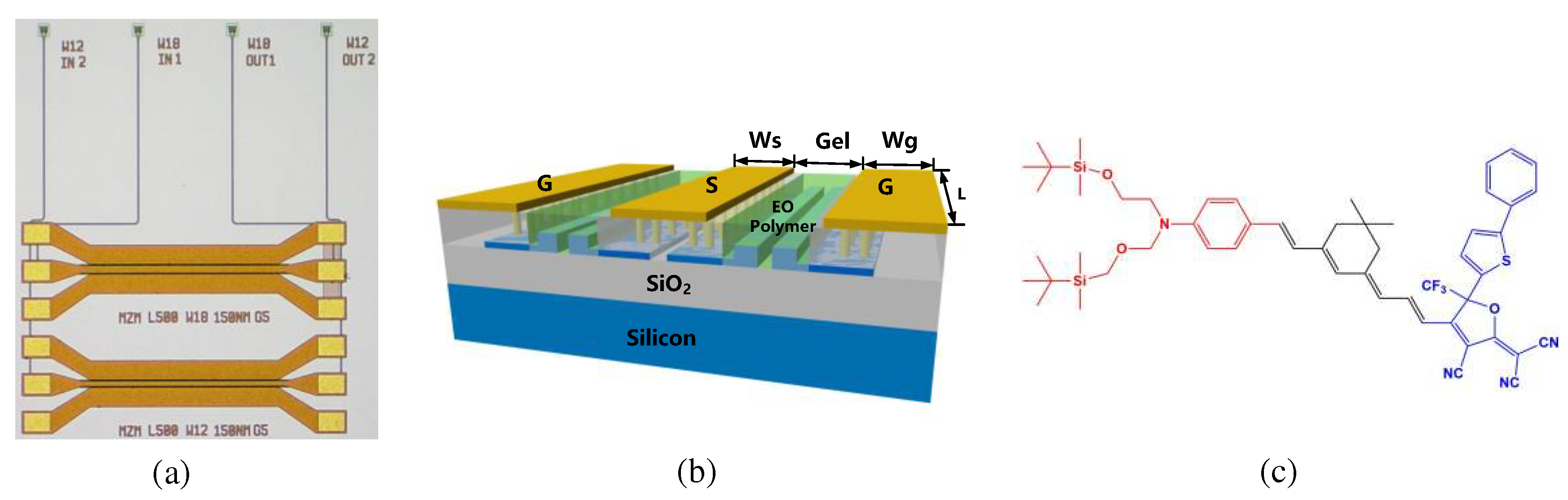
Figure 2.
(a) Schematic diagram of the structure of Slot waveguide; (b) Slot waveguide optical field; (c) Slot waveguide modulated microwave electric field distribution.
Figure 2.
(a) Schematic diagram of the structure of Slot waveguide; (b) Slot waveguide optical field; (c) Slot waveguide modulated microwave electric field distribution.
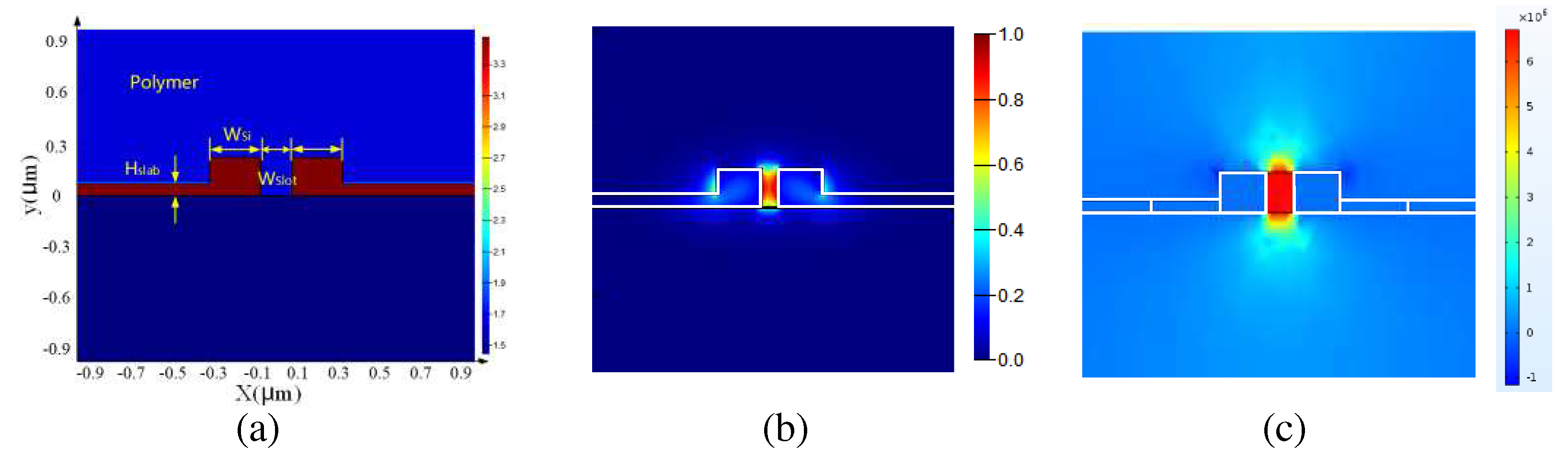
Figure 3.
(a) Schematic of Strip-to-Slot mode converter; (b) Optical field distribution in Strip waveguide (Gauss-like mode); (c) Transmission field distribution of Taper mode conversion; (d) Optical field distribution in Slot waveguide (non-Gauss-like mode).
Figure 3.
(a) Schematic of Strip-to-Slot mode converter; (b) Optical field distribution in Strip waveguide (Gauss-like mode); (c) Transmission field distribution of Taper mode conversion; (d) Optical field distribution in Slot waveguide (non-Gauss-like mode).

Figure 4.
Process flow of SOH modulator fabrication.
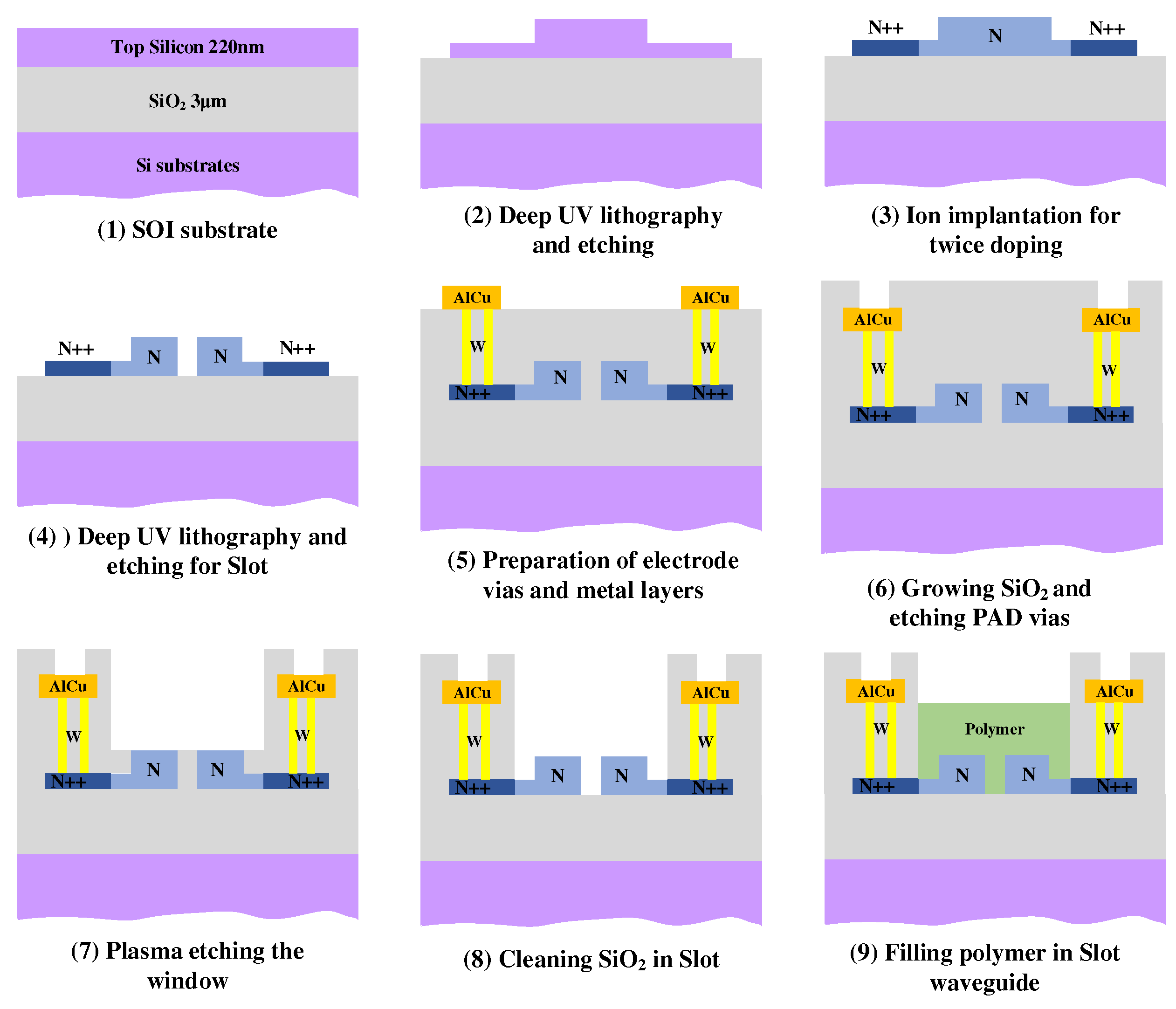
Figure 5.
8-inch wafer of fabricated modulator and micrograph of single block.
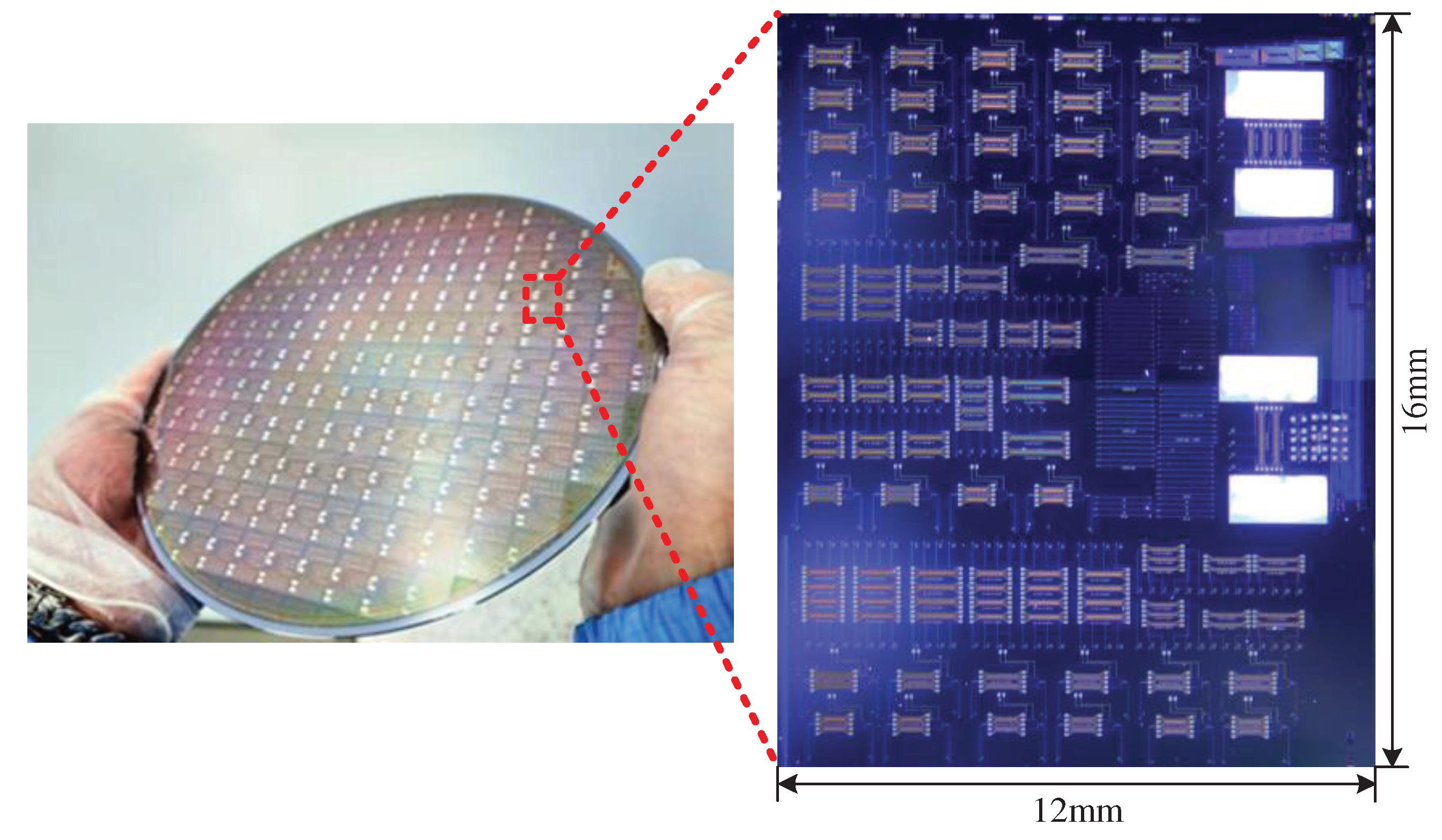
Figure 6.
Schematic of span-coating; (a) Dropwise addition of polymer solution; (b) Spin coating of polymer solution to form a film; (c) Heating and drying to remove solvent.
Figure 6.
Schematic of span-coating; (a) Dropwise addition of polymer solution; (b) Spin coating of polymer solution to form a film; (c) Heating and drying to remove solvent.
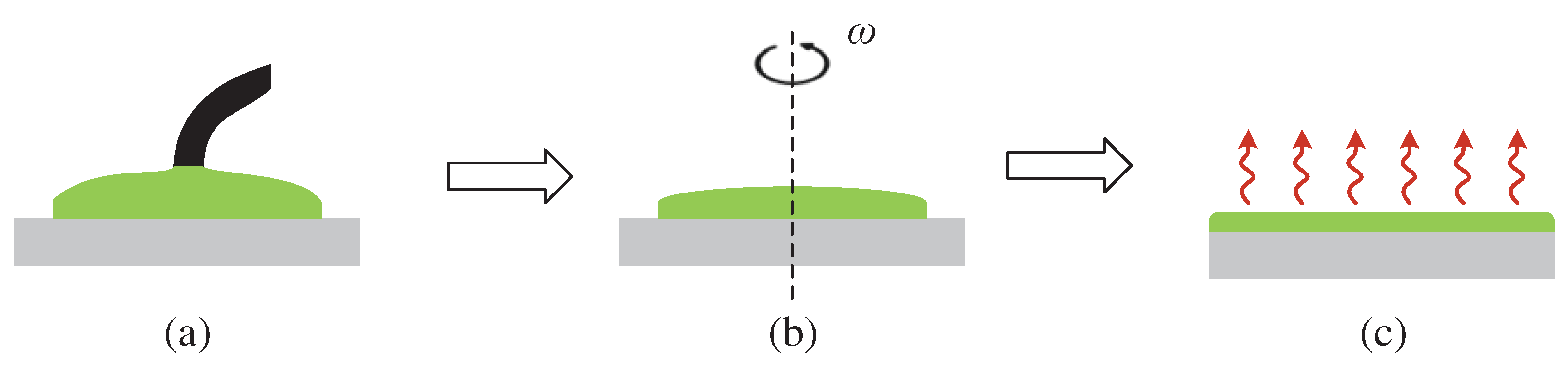
Figure 7.
SEM of Slot waveguide cross-section; (a) Without EO polymer (b) filling with EO polymer.

Figure 8.
Schematic diagram of poling on chip.
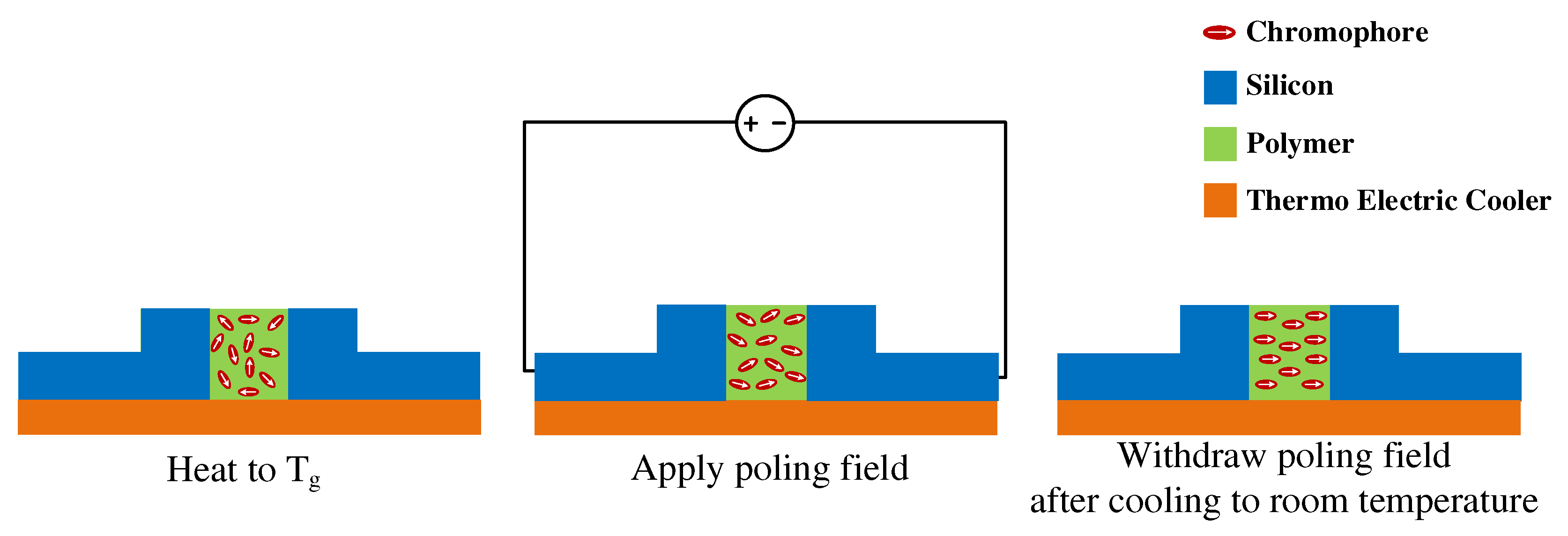
Figure 9.
(a) Cross section schematic diagram of the modulation area with poling DC voltage; (b) Voltage (blue) and temperature (red) during on-chip poling of EO organic material.
Figure 9.
(a) Cross section schematic diagram of the modulation area with poling DC voltage; (b) Voltage (blue) and temperature (red) during on-chip poling of EO organic material.
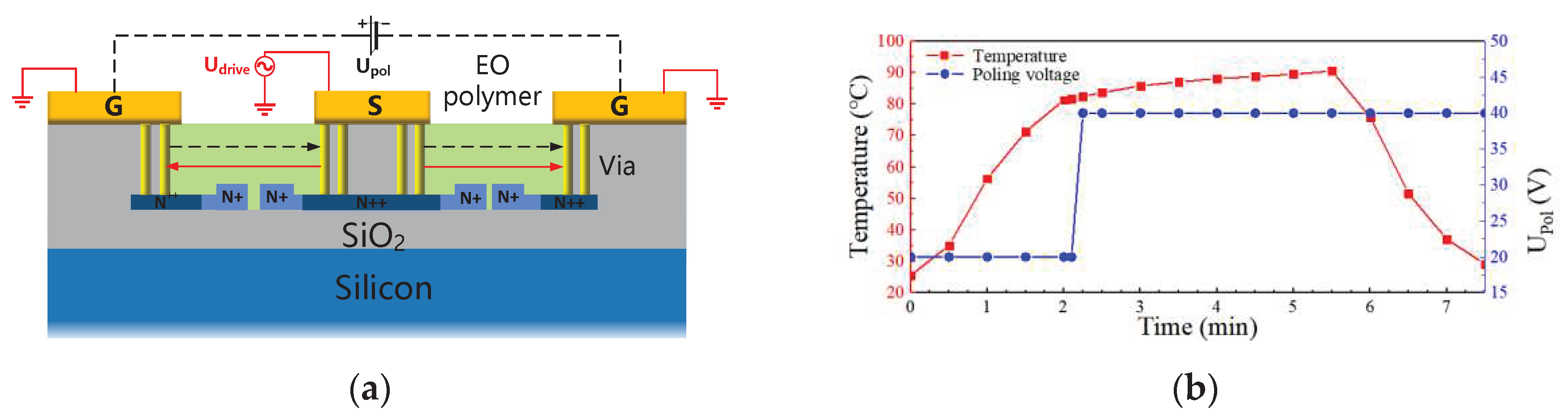
Figure 10.
S-parameters of modulator travelling-wave electrode.
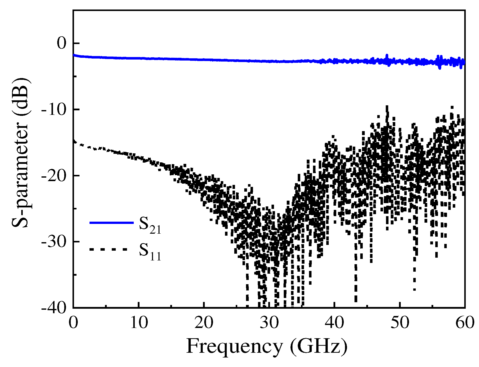
Figure 11.
Distributed parameters of electrode obtained by S-parameters; (a) Electrode characteristic impedance; (b) Microwave effective refractive index.
Figure 11.
Distributed parameters of electrode obtained by S-parameters; (a) Electrode characteristic impedance; (b) Microwave effective refractive index.
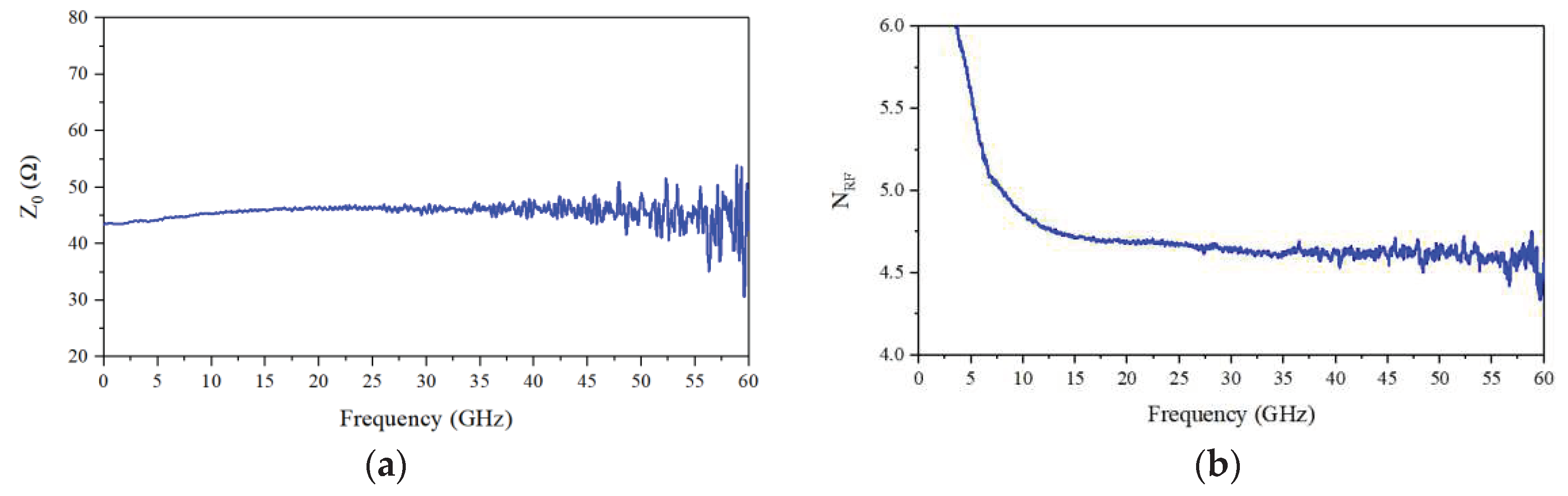
Figure 12.
(a) Experimental setup for measuring RF S21 response; (b)Measured EO S21 of the modulator with modulation length of a 0.5 mm.
Figure 12.
(a) Experimental setup for measuring RF S21 response; (b)Measured EO S21 of the modulator with modulation length of a 0.5 mm.
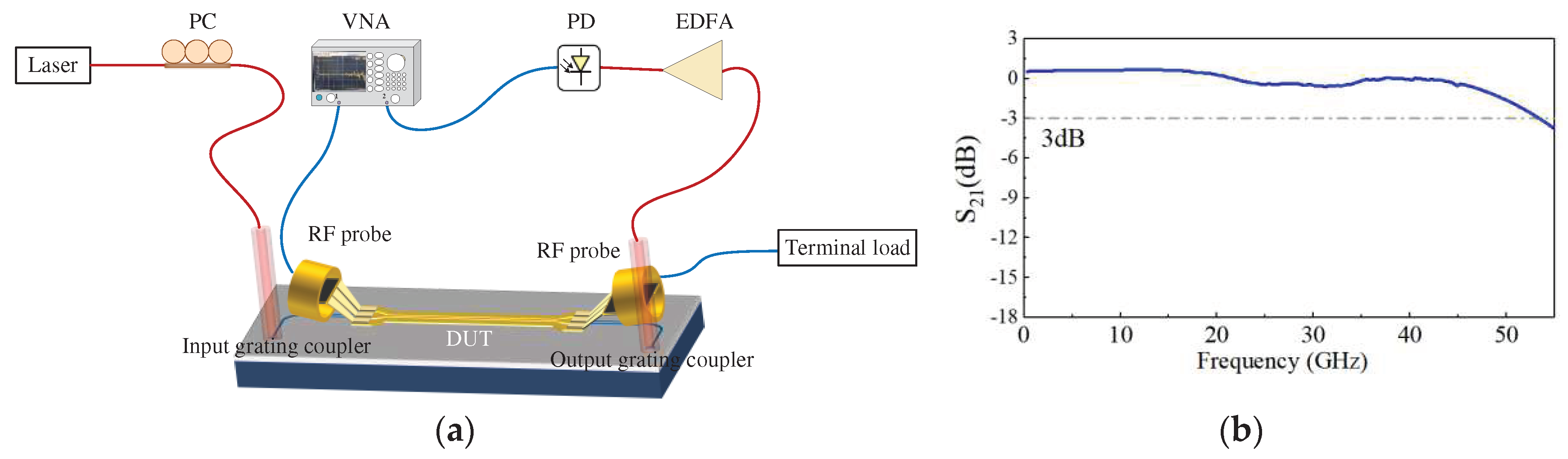
Figure 13.
(a) Experimental setup for measuring half-wave voltage; (b) Measured half-wave voltage of the modulator with modulation length of a 0.5 mm.
Figure 13.
(a) Experimental setup for measuring half-wave voltage; (b) Measured half-wave voltage of the modulator with modulation length of a 0.5 mm.
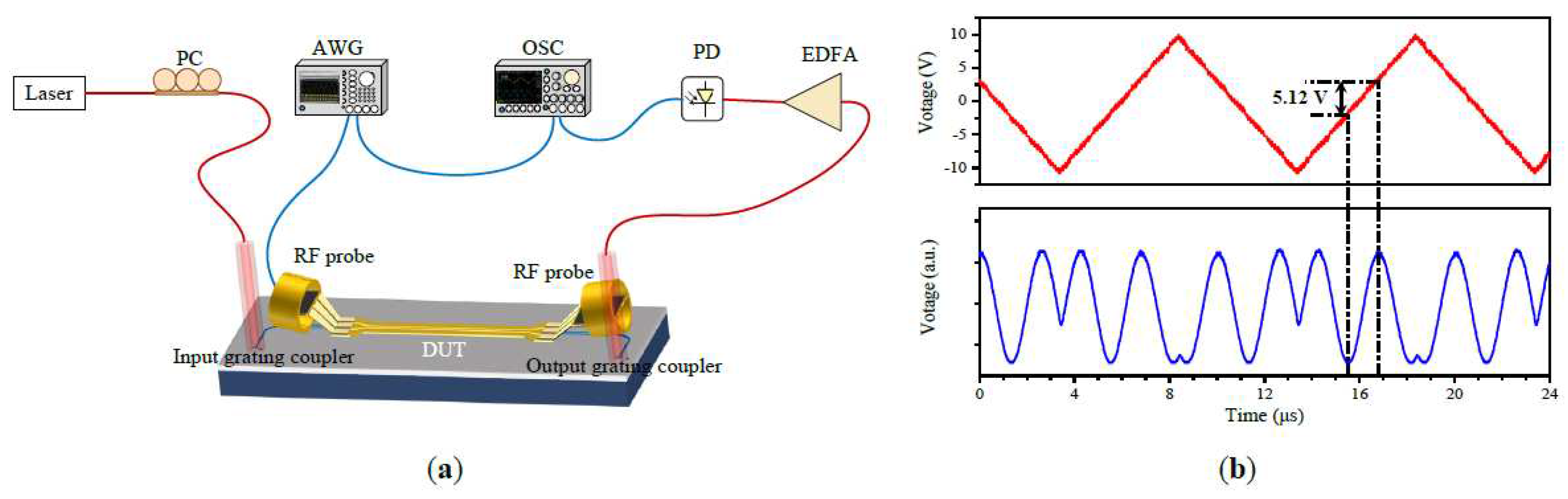
Figure 14.
Time stability of devices in room temperature.
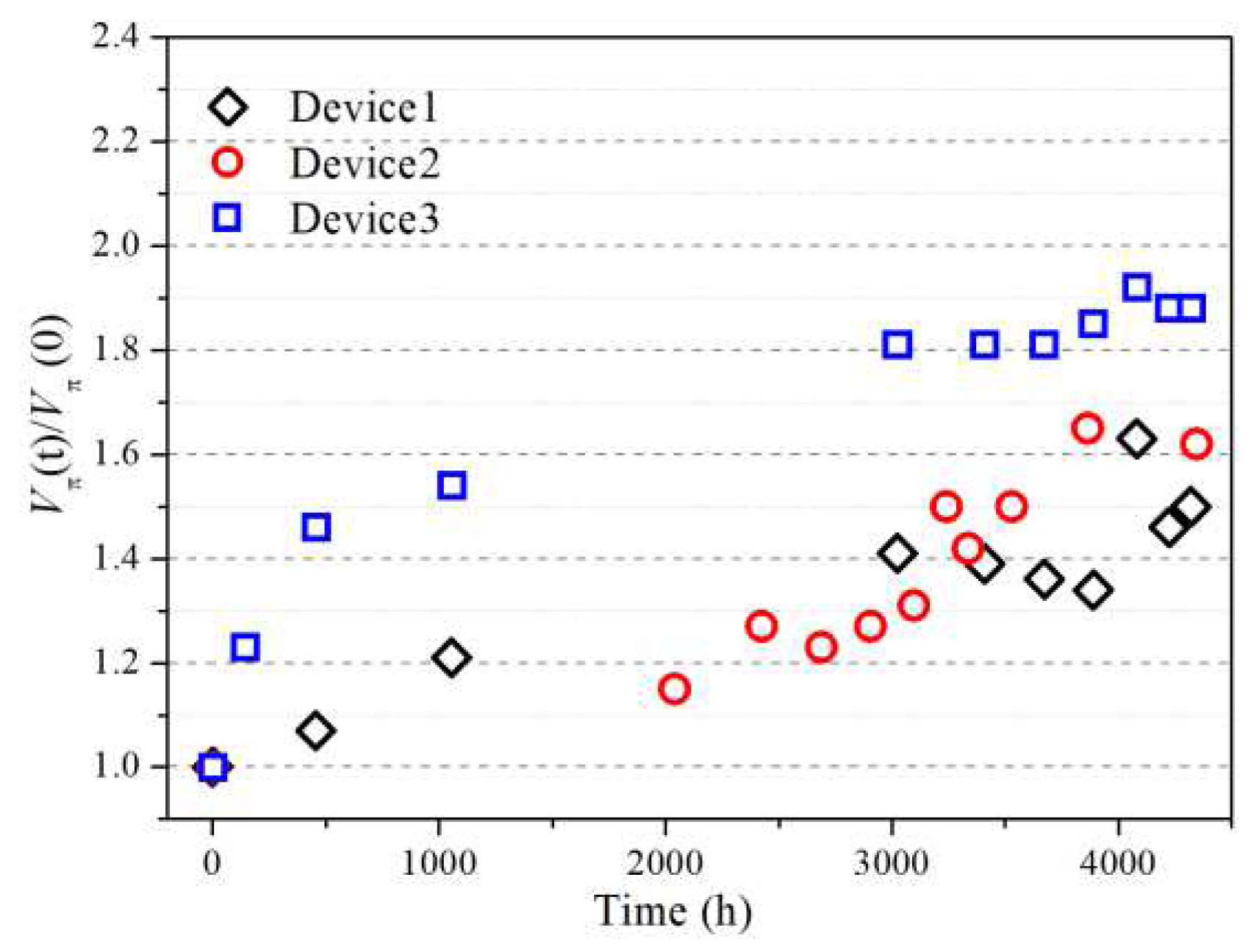
Figure 15.
Schematic diagram of microwave phase shifter based on DP-MZM.
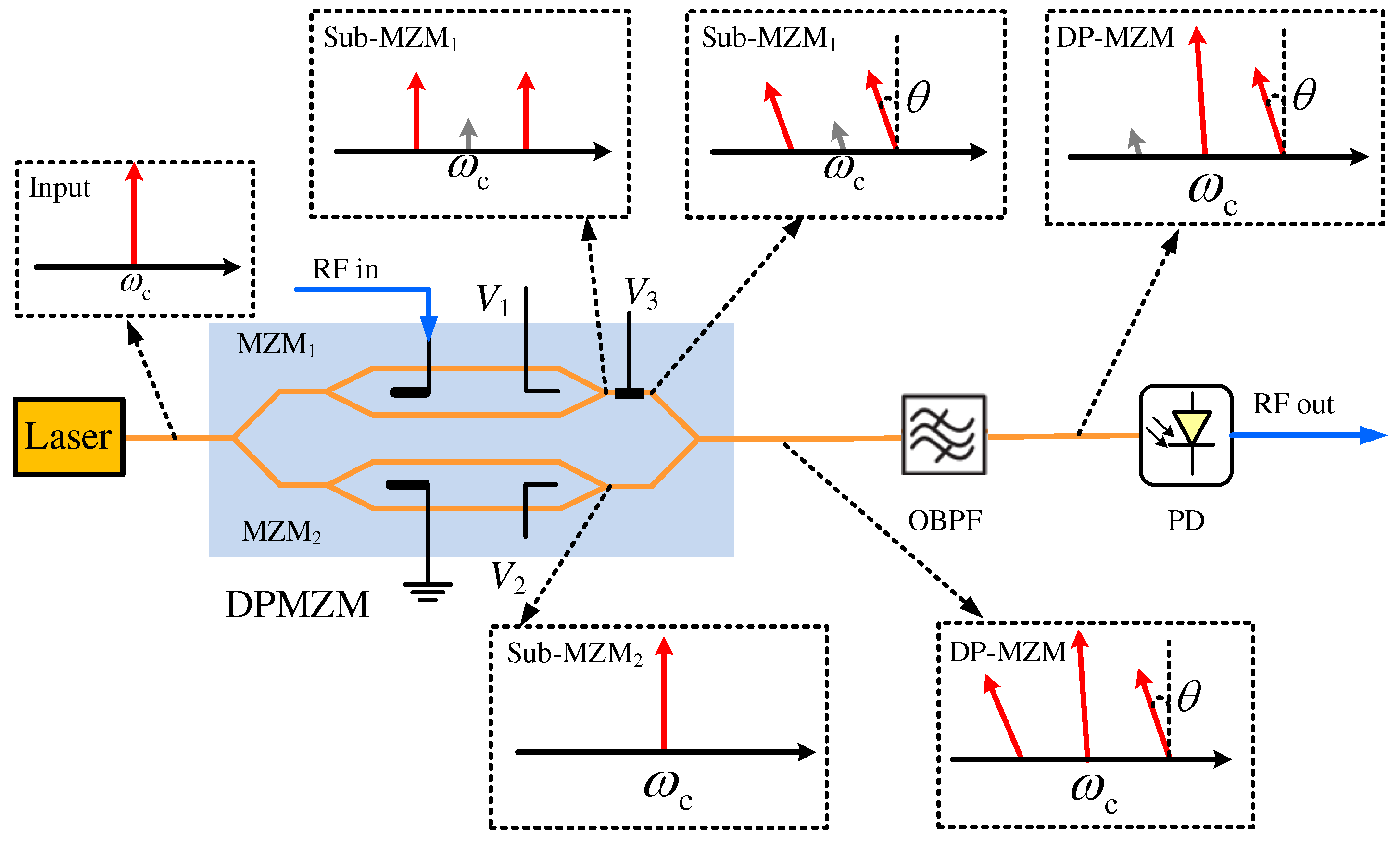
Figure 16.
The variation of the RF phase shift with θ; (a) 1/=40dB, = [10dB, 15dB, 20dB, 25dB, 30dB]; (b) 1/= [10dB, 15dB, 20dB, 25dB, 30dB], 1/=40dB;
Figure 16.
The variation of the RF phase shift with θ; (a) 1/=40dB, = [10dB, 15dB, 20dB, 25dB, 30dB]; (b) 1/= [10dB, 15dB, 20dB, 25dB, 30dB], 1/=40dB;
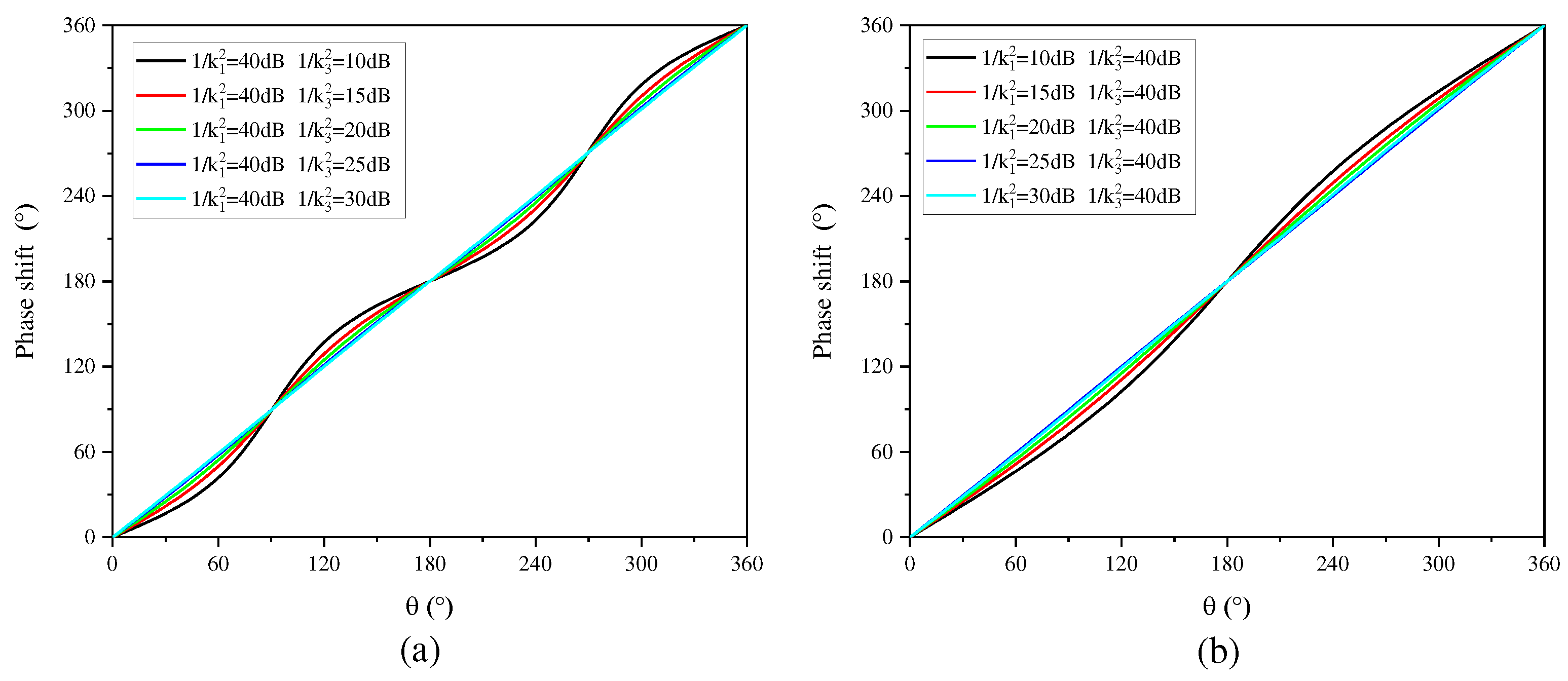
Figure 17.
The variation of the RF power with θ; (a) 1/=40dB, = [10dB, 15dB, 20dB, 25dB, 30dB]; (b) 1/= [10dB, 15dB, 20dB, 25dB, 30dB], 1/k=40dB;
Figure 17.
The variation of the RF power with θ; (a) 1/=40dB, = [10dB, 15dB, 20dB, 25dB, 30dB]; (b) 1/= [10dB, 15dB, 20dB, 25dB, 30dB], 1/k=40dB;
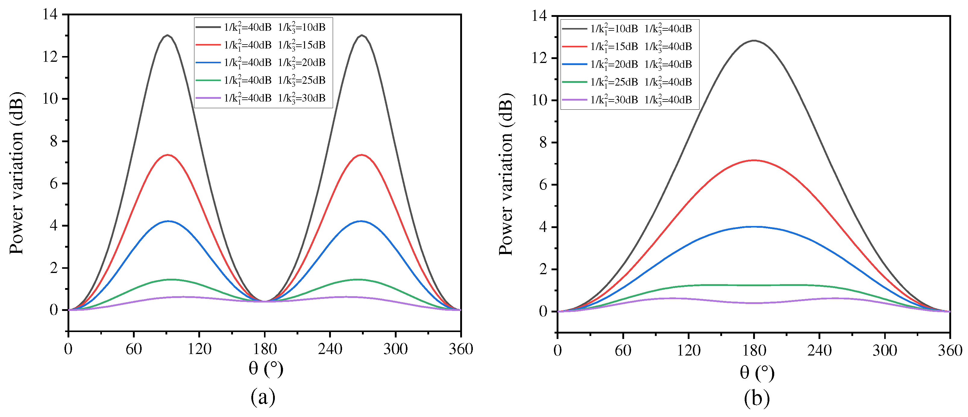
Figure 18.
(a) Output optical spectrum of DP-MZM; (b) The modulated optical signal after OBPF (blue curve) and the OBPF transmission response (black curve).
Figure 18.
(a) Output optical spectrum of DP-MZM; (b) The modulated optical signal after OBPF (blue curve) and the OBPF transmission response (black curve).
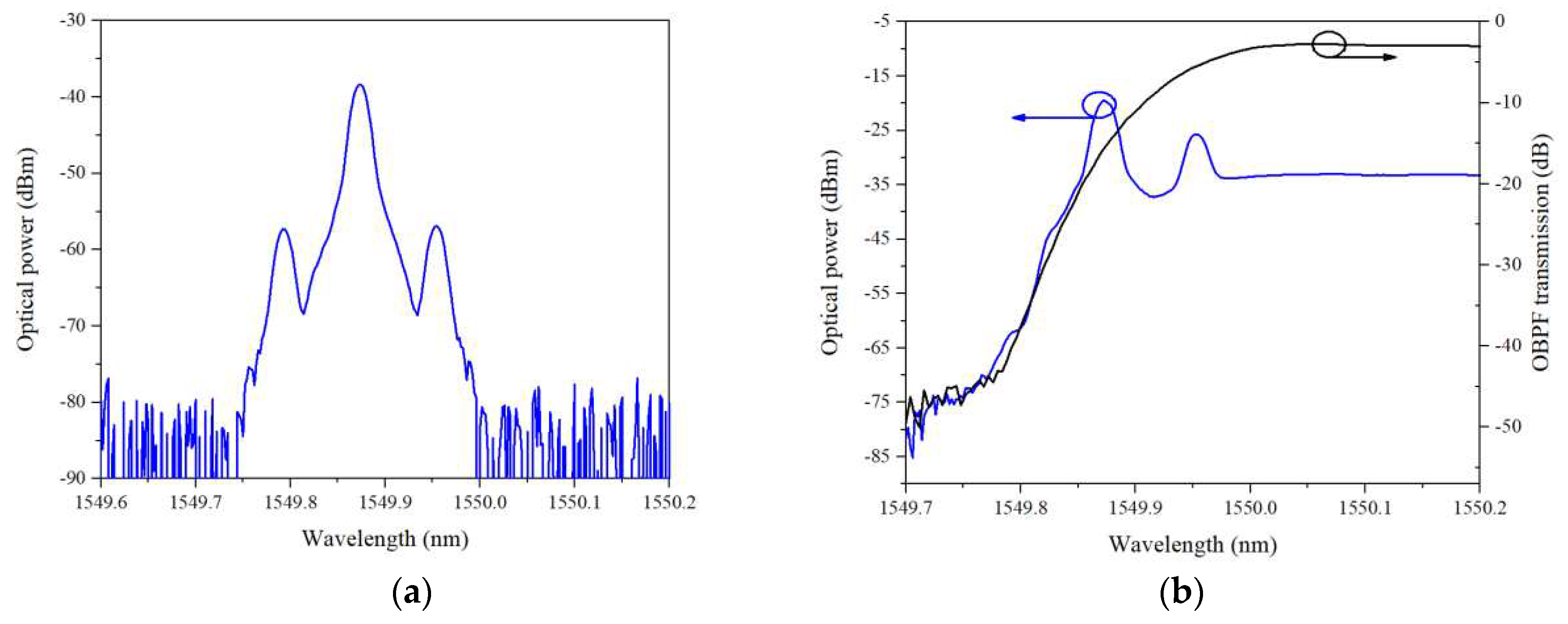
Figure 19.
Measurement results of photonic RF phase shifter; (a)Measured phase shifts for different heating powers over a frequency range from 8 GHz to 26 GHz; (b) Variation of RF phase shift with heat power at different RF frequencies; (c) Variation of RF power with heat power at different RF frequencies
Disclaimer/Publisher’s Note: The statements, opinions and data contained in all publications are solely those of the individual author(s) and contributor(s) and not of MDPI and/or the editor(s). MDPI and/or the editor(s) disclaim responsibility for any injury to people or property resulting from any ideas, methods, instructions or products referred to in the content. |
© 2023 by the authors. Licensee MDPI, Basel, Switzerland. This article is an open access article distributed under the terms and conditions of the Creative Commons Attribution (CC BY) license (http://creativecommons.org/licenses/by/4.0/).
Copyright: This open access article is published under a Creative Commons CC BY 4.0 license, which permit the free download, distribution, and reuse, provided that the author and preprint are cited in any reuse.


