
Submitted:
06 September 2023
Posted:
07 September 2023
You are already at the latest version
Abstract
Thermal fluctuations in two-dimensional (2D) isotropy systems at non zero finite temperatures can destroy the long-range (LR) magnetic order due to Mermin-Wanger theory. Interestingly, the magnetic anisotropy related to spin-orbit coupling (SOC) could stabilize magnetic order in 2D systems. Recently, 2D FexGeTe2 (3≤x≤7) with high curie temperature (TC), as a typical 2D van der Waals metallic ferromagnet, has not only made significant progress in synthetic methods and controlling ferromagnetism (FM), but also actively explored many device applications. In this Review, we introduce six experimental methods, ten ferromagnetic modulation strategies, and three spintronic devices of 2D FexGeTe2 materials. Overall, we have outlined the challenges and potential research directions in this field.
Keywords:
Mermin-Wanger theory
; Fe stoichiometry
; strain
; light-control
; electrical-control
; doping engineering
; twisting
; patterning
1. Introduction
The Mermin-Wanger theory [1,2] asserted that thermal fluctuations occurred in 2D isotropy systems at non zero finite temperatures, which would destroy the long-range (LR) magnetic order. Specifically, only exchange interactions should not generate magnetic order in 2D systems, and magnetic anisotropy [3,4,5] was also needed. Surprisingly, it was found experimentally that low-temperature LR ferromagnetic order could exist in monolayer Cr2Ge2Te6 [4] and CrI3 [5,6]. Subsequently, a vast range of 2D magnetic systems, including metallic (Fe3GeTe2 (FGT) [7,8,9,10,11,12,13,14,15,16,17,18,19,20,21,22,23]), semiconductors (Cr2Ge2Te6 [4,24,25,26,27,28,29,30,31,32], CrI3 [5,33]), and topological insulators (MnBi2Te4 [34]), were successively achieved. Recently, FexGeTe2 (3≤x≤7) has received intense attentions as a metallic and high curie temperature (TC) ferromagnet. Importantly, six synthesis methods including solid-state reaction (SSR) [35,36], chemical vapor transport (CVT) [8,13,37], the flux method [11,21,38,39,40,41,42,43,44,45], exfoliation [14,15,34,46,47,48,49,50], chemical vapor deposition (CVD) [51,52] and molecular beam epitaxy (MBE) [7,53,54,55,56,57,58], have been used to attempt to obtain wafer-scale FexGeTe2 (3≤x≤7) materials with room-temperature ferromagnetism (RTFM). More interestingly, RTFM has been mediated with ten strategies, such as Fe stoichiometry [9,39,51,59,60,61,62,63,64], strain engineering [46,48,65,66,67,68,69,70,71,72,73,74], hydrostatic pressure [75,76,77,78,79,80], light-control [53,81], electrical-control [82,83], proximity effects [56,57,84,85,86,87,88], doping engineering [14,20,38,43,44,60,89,90,91,92,93,94,95,96,97,98,99,100,101,102,103,104,105], intercalation [106,107] or irradiation [108], twisting [109,110] and patterning [16]. Moreover, three devices have also been fabricated based on FGT, mainly including magnetic tunnel junctions (MTJ) [111,112,113,114], tunneling spin valves [18,98,115,116,117], and spin−orbit torque devices [20,118], to enrich their physical properties and develop their spintronic applications.
In this review, we introduce the developments and structures of metallic FexGeTe2 ferromagnet. Subsequently, we have summarized six experimental methods in Figure 1, and the early samples prepared through SSR, CVT and flux method were mainly bulk single crystals. Last, we have outlined the challenges and potential research directions in this field.
2. Crystal Structure and Band Structure of Ferromagnetic FexGeTe2
The Fe3GeTe2 monolayer [46] included five atomic layers in Figure 2(A). In details, Te atoms were located at the bottom and top layers, while Fe (I) atoms were located in the second and fourth layers. Notably, the intermediate layer was composed of Fe (II) atoms and Ge atoms. In particular, the local magnetic moments of Fe atoms for FGT monolayer were 1.723 µB and 1.005 µB through density functional theory-local density approximation (DFT-LDA) calculation, and may be related to the several partially d-band occupied passing through the Fermi level. Similar to its bulk, FGT monolayer was metallic as shown in Figure 2(B). Its band structures near the Fermi level were mainly due to the contribution of the Fe 3d orbitals. Moreover, it could be confirmed that the FGT monolayer had the itinerant FM order according to Stoner’s criterion [46,119]. More importantly, the Stoner model related to itinerant electrons could be used to better elucidate the spontaneous magnetization in most of 2D metallic ferromagnets. In addition, the number ratio of Fe3+ to Fe2+ in 2D FexGeTe2 [62] was related to the x value, as shown in Figure 2(C-D). When the value of x was 3, the ratio of Fe3+/Fe2+ was 2:1; However, when the x value was 5, only Fe3+ was present. As shown in Figure 2(E), the electronic band structures of all the FexGeTe2 systems were metallic, be similar to 2D FGT.
3. Synthesis of Metallic FexGeTe2 with FM
3.1. Solid-State Reaction (SSR)
Solid-state reaction (SSR) is an experimental method for preparing bulk FGT crystals. As early as 2006, Deiseroth et al. [35] successfully prepared FGT crystals with the hexagonal plates using SSR, which exhibited new air-stability and black-metallic. Through magnetic testing, it was found that below 230 K, it exhibited FM; while above 230 K, it exhibited Curie-Weiss paramagnetism behavior. After increasing annealing, black Fe3-δGeTe2 (0<δ<0.3) polycrystalline powders could be easily obtain with SSR. In details, Fe1 and Ge1 atoms are in different coordination environments Figure 3A-B, and two layers consist of its unit cell. In details, its lattice parameters increase monotonically with decreasing δ (Figure 3C). But when δ exceeds 0.3, FeTe2 as an impurity phase will appear. Its magnetic phase transition temperature (Figure 3D) is about 240 K. Furthermore, its saturation behavior (inset in Figure 3D) slows down under high magnetic fields, which is different from ordinary ferromagnets.
In order to obtain large quantity and high-quality FGT single crystal , Li et al. [120] designed a new experimental method of solid-phase sintering followed by recrystallization (Figure 3E-H). As-grown plate-like sample (~10g) is a layered single crystal with a smooth and complete surface, and its size can reach up to 8.5 mm. By intercalating sodium into as-grown FGT (Figure 3I-J), Weber et al. [106] could raise its TC to 350 K. After intercalation, the sample retained obvious layered features, with edge lengths of grain size ranging from 10-50 μm.
3.2. Chemical Vapor Transort (CVT)
One main difference from SSR was that CVT often used iodine [8,13,14,15,17,37,39,59,118] or TeCl4 [12] as the transport agent in Figure 4. However, the samples obtained with SSR and CVT were both bulk single crystals in the inset of Figure 4A-B. Previous studies mainly focused on the magnetic microstructures of quasi-2D FGT. Inspired by the prediction that monolayer FGT could be mechanically exfoliated [46], soon after, Chu et al. [15] and Zhang et al. [14] respectively obtained monolayer FGT samples with the assistance of Au film or Al2O3. Interestingly, Zhang et al. [121] exfoliated monolayer FGT from the most possible cleaving plane (001), with a thickness of 1.75 nm and the nearest neighbor atomic spacing of 0.338nm, which was very consistent with the lattice constant (a= 0.399nm; c=1.63nm) of FGT crystal. However, thin layer FGT was very prone to deteriorate in air, and the device fabrication processes (Figure 4C-E) needed to be carried out in a glove-box [49]. Importantly, many novel physics effects such as patterning-induced [16], gate-tunable [14], and layer-dependent FM [15] have been recognized.
3.3. Flux Growth
Flux method [122,123,124] is a commonly used method for preparing single crystals. For example, Canfield et al [122,123] grew a wide variety of single crystal binary or ternary intermetallic compounds from molten flux solutions. However, the thickness and lateral size of the samples couldnot be accurately controlled, which still required mechanically exfoliating to obtain thinner samples when fabricating FGT devices.
Interestingly, Gong et al. [44,45] proposed a universal flux-assisted growth (FAG) method (Figure 5D-E) to synthesize the FexGeTe2 and MyFe5-yGeTe2 (M = Co, Ni) nanosheets on various substrates (Figure 5F-L). More importantly, the sample thickness and lateral size (Figure 5M-Q) of FGT could be precisely controlled by growth temperature (Figure 5R) or cosolvents (Figure 5S). Although FGT samples with a thickness of 5-10 nm (Figure 5T) were prepared on various substrates, in order to obtain atomically thin materials (ATMs), a confinement environment must be provided through two substrates. Up to 80 layered and non-layered ATMs [45] have also been successfully synthesized by FAG, which provided a new strategy for preparing wafer-scale 2D materials.
3.4. Exfoliation
3.4.1. Mechanical Exfoliation
The conventional mechanical exfoliation [126,127] could cleave thin FGT flakes onto SiO2/Si substrates, but its thinnest thickness was around 4.8nm. After depositing Au onto SiO2/Si substrate, thinner samples could be obtained, and the Au substrate would improve the yield of various thin layers of materials, including graphene [128,129], MoS2 [47,130,131,132,133], WSe2 [47,130,134], Bi2Te3 [130] and FGT [15,47]. Nevertheless, only a small amount of material could be exfoliated to a monolayer, which hindered the development of 2D magnetic materials. Notably, an Al2O3-assisted exfoliation was also designed to produce monolayer FGT [14] and MnBi2Te4 [34] single crystals. More importantly, when the sample was thinned from bulk to a monolayer, its TC would decrease from 180 K to 20 K.
3.4.2. Liquid-Phase Exfoliation
Although many methods including SSR [106], CVT [14,15,17,19,59,118,121,135], flux [39,43,44,45] and MBE [7,53,54,55,56,57,58,64,136], have been used to prepare 2D FGT, there was still a lack of an economical method to prepare large-scale of few or single layer FGT nanoflakes. As a typical example, Ma et al. [50] developed three-stage sonication-assisted liquid-phase exfoliation (TS-LPE) (Figure 6A) to achieve large-size semiconductive FGT nanoflakes. After ball milling, the sample size and thickness (Figure 6B-C) will be reduced by milling time (Figure 6G), exposing more boundaries. Stirring would make the interlayer spacing expand (Figure 6C-D), weakening the interlayer force to facilitate detachment and obtain high-integrity nanoflakes. In addition, XRD analysis [137] (Figure 6H-I) also reflected the evolution of interlayer spacing. The expansion of interlayer spacing would cause FGT unit cell to move away from the equilibrium state in the c-direction (Figure 6J), making them unstable and prone to spall. More interestingly, the oxidation on the surface layer altered the electronic structure of FGT system, making FGT sample semiconductive and different from the metallic FGT prepared by other methods.
3.5. Chemical Vapor Deposition (CVD)
So far, researchers mainly used CVT to prepare 2D magnetic bulk single crystals, which were then exfoliated into atomic layers to prepare devices. However, poor control of the number of layers and limited sample size have hindered the development of 2D magnets. As a typical example, Liu et al. [51] designed a confined space chemical vapor deposition (CS-CVD) to prepare 2D FGT or F5GT ferromagnets. They found that the optimal growth temperature was 570-580℃, with an optimal distance of 10 cm between Si/SiO2 substrates and Te precursor. When the thickness of F5GT flakes changed from 4 nm to 1 nm, its TC would decrease by 100K. Very recently, Liu et al [52] also introduced a general competitive-chemical-reaction-controlled CVD method for producing FGT crystals. The sample was a single layer with a grain size of ~50 μm.
3.6. Molecular Beam Epitaxy (MBE)
Notably, wafer-scale single crystalline FGT thin films (Figure 7) were grown on (0001) sapphire, (111) GaAs and (111) Ge substrates by the molecular beam epitaxial (MBE) [7,54,55,56,57,138] technique. Interestingly, in situ reflection high-energy electron diffraction (RHEED) exhibits the same periodicity (Figure 7B), and can complete one layer of growth in approximately 111 seconds. Similary, the same 2D growth mode (Figure 7H, I) was also observed during the FGT and FGT|Bi2Te3 grown. Furthermore, the layered characteristics and a interlayer spacing of 0.82 nm could be confirmed through cross-section high-resolution transmission electron microscopy (HRTEM) (Figure 7D-F, O and P). In addition, Fe, Ge, and Te elements are uniformly distributed on the cross-section, and their atomic ratios can be determined by X-ray spectroscopy (EDX) mapping (Figure 7P).
4. Controlling FM in metallic FexGeTe2 (3≤x≤7)
4.1. Fe stoichiometry
The earliest discovery was that FM in polycrystalline FGT bulk [9] was related to Fe content (Figure 8). The higher the Fe content, the larger the lattice constant of the a-axis and the smaller the lattice constant of the c-axis (Figure 8A). Single crystal samples also have similar results with polycrystalline samples. More interestingly, the TC (Figure 8B) and MS decreased with the decrease of Fe content. Subsequently, ferromagnetic F4GT [44,59,64] and F5GT [39,42,44,51,60,139,140,141,142,143,144,145,146] materials were also obtained in experiments.
However, most of previous reports have focused on FGT materials with a single Fe stoichiometry, and there have been few studies on FexGeTe2 materials using the same experimental method. Interestingly, theoretical calculations [61] revealed that as the Fe content increased, the interlayer gap gradually increased, and the magnetic anisotropy of its monolayer changes from out-of-plane (FGT) to in-plane (F4GT and F5GT).
Although previous reports have made significant progress in 2D FexGeTe2 system, the mediation of magnetic anisotropy and magnetic nature remain unresolved. Very recently, Liu et al.[62] brought forward a valence-dependent magnetic exchange model to explain the complex magnetic phase in FexGeTe2 system. Furthermore, the magnetic moment and MAE (Figure 9A) were almost linearly correlated with Fe2+/Fe3+. Specially, Fe3+ had a greater impact on magnetism, reducing the magnetic anisotropy energy in F5GT. Based on MAE and J, the TC could be estimated with the 2D Heisenberg model. When x was greater than 4, the TC was much higher than RT (Figure 9B).
More importantly, the results obtained through different calculation methods [63] have significant differences, especially when compared with experimental results. As x increased, its easy axis direction (shown in the black arrows) and the highest exchange interaction changed from off-plane to in-plane (Figure 9C-F). Moreover, there were significant differences in the magnitude of exchange interaction obtained by different calculation methods (GGA+DMFT, GGA and GGA+U), among which the results calculated through GGA+U were overestimated in Figure 9G-J. Interestingly, MAE (Figure 9K-M) also exhibits a similar evolution from off-plane to in-plane. However, for different F5GT (UUU or UDU) configurations (Figure 9M-N), the calculation results varied greatly. It was very obvious that the TC calculated by GGA+DMFT (Figure 9O-R) was underestimated, while the result calculated by GGA was overestimated, compared to Figure 9B.
. Reprinted with permission from Ref.[63], Copyright 2023, Springer Nature.
4.2. Strain Engineering
Strain engineering is indeed an efficient stragety to modulate the FM of 2D materials [66,67,147]. However, previous theoretical works have focused on applying strain to FGT supercells by changing lattice constants [46,69,70,72,148], and calculating the exchange coupling, magnetic anisotropy, and magnetic moment of strain through ab initio density functional theory (DFT). Furthermore, the TC could be estimated by mean field theory (MFT) [10,59,63,149,150,151], random phase approximation (PRA) [149,151], or Monte Carlo (MC) [150,151,152,153] simulation. Very recently, Miao et al. [48] and Yan et al. [71] loaded FGT nanoflakes to a three-points bending experimental set-up, and applies uniaxial tensile strain to the sample on a polyimide (PI) or polyvinyl alcohol (PVA)/ polyethylene terephthalate (PET) flexible polymer substrate by moving needle. Moreover, the magnitude of the applied strain could be calculated using the following formula [48,71,154]:
Note that, T and R were the film thickness and bending radius, respectively. Surprisingly, after 0.32% strain was applied, the coercivity increases by 150% [48], far greater than the improvement in HC of other traditional magnetic materials [155]. More importantly, its TC could be increased to 400 K [71] through uniaxial strain, which would further promote the development of its practical applications.
4.3. Hydrostatic Pressure
Actually, tuning the exchange coupling and magneto-crystalline anisotropy by hydrostatic pressure was also a commonly used method for regulating 2D magnetism, which had been achieved in Cr2Gr2Te6 [156,157], CrI3 [33,158], and FGT [76,77,78] systems (Figure 10). The ferromagnetic evolution of FGT nanosheets under different pressures can be revealed through in situ magnetic circular dichroism (MCD) spectroscopy (Figure 10B).
Furthermore, the magnetic hysteresis loop at 30 K exhibited a rectangular shape below 7 GPa, while its loop presented an 8-shaped skewed shape above 7.3 GPa (Figure 10C-D). Moreover, Tc will increase as the pressure further decreases (Figure 10E), which may be related to the strengthening of the exchange interactions. As another typical example, Tc and the magnetic moment also increased with the decrease of hydrostatic pressure (Figure 10F-I). It was evident that increasing pressure reduced the length of Fe-Fe bond, which inhibited magnetization through modification the exchange interactions. In addition, a monotonic relationship between Tc, the magnetic moment and pressure was also found in Fe-deficient FGT sample [76], similar to FGT system. Interestingly, pressure will modify the metallic form of Fe3-xGeTe2 to nonmetallic.
4.4. Light Control
As a typical example, continuous modulation of monolayer layered TMDs without intrinsic magnetism, including MoS2 [159], WS2 [159], and WSe2 [160], has been achieved through the optical approach. Recently, Tengdin et al. [81] demonstrated that spin polarization was transferred from Mn sublattices to Co on Heusler compound Co2MnGe via femtosecond laser pulse, which was closely related to the wave function of an electrons before and after being excited by light. The ultrafast spin transfer caused by the instantaneous incident light on the material not only occurs in Co2MnGe, but also was a common feature of many materials. Notably, Xu et al. [53] reported that the magnetic anisotropy energy (MAE) and Tc were mediated with a femtosecond laser pulse in Figure 11. The optical doping effect alters the electronic structure of FGT, thereby affecting exchange interactions, Tc, and MAE. According to Figure 11(B), the Tc of FGT was estimated to be ~200 K. Under the excitation of femtosecond laser, electrons transitioned from occupied state to unoccupied state, causing the Fermi level EF to shift downwards and crossing the enhanced density of states (DOS) in Figure 11D. Furthermore, some clear magnetic hysteresis loops (Figure 11E-G) at room temperature (RT) can be observed in FGT samples with different thicknesses through MOKE measurements (Figure 11C). The Tc of FGT could be increased to above RT through light control, providing many opportunities for the development of spintronic applications for 2D magnets.
4.5 Electrical Control
Previous studies have shown that electric fields modified the magnetism of metal films [161,162,163] and Fe/MgO junctions [164] by influencing the behavior of the electrons. Recently, Wang et al. [82] calculated the effect of electric field on the magnetic anisotropy of monolayer FGT in Figure 12A-C. The effect of orbital splitting caused by electron doping on magnetic anisotropy was more pronounced; while the influence of hole doping related to orbital occupation was relatively weak. In addition, the change in magnetic anisotropy (Figure 12C) was more obvious in the single-gate configuration (Figure 12B).
Additionally, the generation of negative differential conductance (NDC) [83]can also be driven by a local electric field in FGT (Figure 12D). Furthermore, the three peaks in the Fe d orbits underwent significant shifts under the electric field, as shown by the green line in Figure 12(E-G). As the electric field was enhanced, the off-plane FM of FGT weakened, resulting in a decrease in MAE (Figure 12H). Importantly, In single-layer FGT, the electric field induces charge transfer in monolayer FGT in the field direction (Figure 12I). Therefore, applying an electric field has become an effective way to mediate 2D FM.
4.6. Proximity Effects
Proximity effects [84,165,166,167,168,169] also dominated in 2D materials. For example, by adjacent 2D magnetic materials to bulk semiconductor substrate [170] or 2D materials with strong spin-orbit coupling [171], their magnetism can be enhanced. Intriguing, zhang et al. [84] fabricated the antiferromagnetic FePS3(FPS)/ferromagnetic Fe3GeTe2(FGT) heterostructures and found the enhancement of Tc and HC through proximity coupling effects. Furthermore, FPS/FGT/FPS has slightly different modulation of Hc compared to FPS/FGT, which was related to AFM-FM coupling. After integration with a topology insulator Bi2Te3 [56], the Tc of FGT could be increased to 400 K by enhancing the intralayer spin interaction, mainly due to the interface exchange coupling effect. More interestingly, the long-range magnetic order induced by topology triggered by femtosecond laser pulses [57] could also be maintained at room temperature.
In addition to the aforementioned methods for mediating magnetism, additional means [7,14,33,48,53,56,57,71,75,76,77,78,156,157,158,171] were required. Directly exfoliating FGT nanosheets [87] onto different substrates could also tailor magnetism as shown in Figure 13. Intriguingly, FGT samples with different thicknesses all exhibited magnetism, while samples on different substrates exhibited different TC, indicating that the substrate has a modulation effect on TC. Furthermore, the lattice distortion and charge redistribution at the interface were related to substrate-induced FM, and this mechanism needed further exploration. Importantly, substrates not only affected the growth of 2D materials, but also determined their performance [172,173].
4.7. Doping Engineering
4.7.1. Doping with 3d Transition-Metal
Doping 3d-transition metal atoms was an effective strategy for controlling magnetism [65,68,89,174,175,176,177,178]. Theoretical calculations shown that almost all 3d-transition metal atoms (except for Co atom) [96] were more inclined to replace Fe1 atoms (Figure 2A). The charge transfer generated by doping atoms would weaken the magnetic moment of Fe atoms, while the weakening effect of Fe1 atomic magnetic moment was more significant. However, the magnetism increases after doping with Co atoms, which may be related to the a-axis lattice constant shrinking. In experiments, doping 3d-transition metal atoms in bulk single crystal samples in Figure 14 was usually achieved through CVT [92] or self-flux [38]. Doping Ni atoms suppressed ferromagnetic order, which rapidly decreased with the increase of doping amount. The TC decreased from 212 K to 50 K, and after reaching 0.44, the magnetic moment remained almost constant (Figure 14A-B). Furthermore, long-range magnetic order was suppressed and subsequently transformed into a glassy magnetic phase (Figure 14C). However, doping Co atoms (Figure 14D) could cause an increase in HC (Figure 14E) and the appearance of hard magnetic phases (Figure 14F), which was related to the movement of pinned domain walls [8].
As another typical example, bulk F5GT single crystals was also doped with Co atoms through CVT [94,95] in Figure 15. As the doping amount of Co increases, it can drive the evolution of lattice and magnetism (Figure 15B). But the nominal doping concentration (Figure 15C) was slightly different from the measured one, with only a specific concentration being more consistent. After Co atoms were doped into the lattice, resulting in the slightly increase of their interlayer spacing (Figure 15D). Indeed, a phase transition from FM to AFM occurred at high doses of doping in Figure 15(E-G). Indeed, a phase transition from FM to AFM occurred at high doses of doping in Figure 15(E-G). However, Tian et al. [95] found that doping 20% Co could increase its TC to 337 K, and induce complex magnetic phase transitions at higher Co doping levels. More importantly, 2D CoyFe5−yGeTe2 (Figure 15I) and NiyFe5−yGeTe2 (Figure 15J) nanoflakes with hexagonal shape were prepared by flux-assisted growth (Figure 15H) [44]. As shown in Figure 15H-M, various elements in the nanosheets were evenly distributed through energy dispersive spectroscopy (EDS) elements mapping, and there were significant differences in the energy spectrum of samples doped with different Co, with a doping amount of up to 66.7%. Furthermore, the doping of Co atoms caused a decrease in TC, and as the doping amount increased, its TC would decrease even lower (Figure 15N). In addition, the magnetic anisotropy has also undergone significant changes (Figure 15O-P). Similarly, Ni doping could also cause a decrease in TC. In other words, the higher the content of Fe, the higher its TC.
4.7.2. Doping with Non-Metallic Atoms
Not only could Fe atoms be substituted with Co or Ni atoms [38,44,92,94,95,96], but doping could also be achieved by replacing Ge atoms with As atoms [91,97]. The doping of As atoms caused a decrease in the a-axis lattice constant and an increase in the c-axis lattice constant, thereby reducing the density of spin states below fermi level and resulting in a decrease in TC [91]. Furthermore, its MS has decreased linearly with the increase of doping amount in polycrystalline Fe3-yGe1-xAsxTe2 (0≤x≤0.85). Similarly, the expansion of F5GT unit cell [97] in the c-axis direction and the contraction in the ab plane were also observed after As atoms doping. In addition, its TC and MS have decreased in polycrystalline Fe5Ge1-yAsyTe2 (0≤y≤1), similar to Fe3-yGe1-xAsxTe2 (0≤x≤0.85) samples. Moreover, the stacking disorder caused by doping induced local AFM coupling, thereby reducing its MS.
4.7.3. Electron Doping
Remarkably, Deng et al. [14] found that the TC of monolayer FGT could be raised to RT through ionic gate, providing a new idea for mediating 2D FM. Although they did not fully explain the relationship between its ferromagnetism and electron doping, this strategy was fully recognized. Not long after, gate-control was implemented to regulate magnetic resistance [98], magnetic phase [60,100], and interlayer coupling [99,101,179]. Furthermore, the TC and HC in FGT flakes [100] were decreased after Li+ doping from lithium-ion conducting glass-ceramics (LICGC). In addition, electron doping influenced the Fe-Ge plane in the middle of monolayer FGT, weakening the resistance and enhancing its TC [104]. As a typical example, the modulation of interlayer coupling was achieved by fabricating FGT hall devices on solid-state proton conductors (Figure 16A). Interestingly, they discovered clear exchange-bias (EB) by changing the gate voltage (Figure 16B). which may be related to the presence of AFM phase at low temperatures (Figure 16C). However, a random exchange bias (Figure 16D) occurs after applying a higher gate voltage. Furthermore, the exchange bias and coercivity (Figure 16E-F) have undergone a complex evolution with the measurement times, but there have also been cases of small EB and large coercivity. More importantly, the type of AFM-FM interface coupling determines the positive and negative exchange bias (Figure 16G).
Additionally, Tan et al. [60] achieved a high electron concentration doping of F5GT through solid proton conductor (Figure 16H-I). When a positive bias voltage was applied, the transport properties does unchange; while a negative bias voltage was applied, there was a significant change in transport properties caused by proton intercalation, especially when it reached -5 V, and the anomalous hall loop disappeared (Figure 16J), accompanied by the appearance of magnetic phase transition. Moreover, different calculation methods have revealed that electron doping achieves a reversal of hall conductivity and phase transition (Figure 16L-N). Therefore, electron doping or protonic gating was indeed an efficient method of controlling magnetis phase transition. Furthermore, Tang et al. [101] also found that magnetic anisotropy in F5GT was continuously mediating with electrolyte gating. Importantly, the screening effect of itinerant electrons driven magnetic anisotropy to switching from off-plane easy axis to in-plane easy axis.
4.7.4. Hole Doping
Inspired by the gate-mediated RTFM in FGT thin flakes [14], many attempts have been implemented to control its ferromagnetism through hole [43,93,105] or electron [43,93,104] doping. In particular, the magnetic anisotropy in exfoliated Fe2.75GeTe2 flake (Figure 17A-B) was inhibited by hole doping, resulting in a decrease in HC (Figure 17C). The magnetic anisotropy could undergo a 93% attenuation, but the change in magnetic moment was very small as shown in Figure 17D. Furthermore, the electronic structure of Fe2.75GeTe2 single crystals changes caused by hole doping driven significant changes in magnetic anisotropy. In addition, another report [93] suggested that hole doping was beneficial for maintaining long-range ferromagnetic order.
Remarkably, the intrinsic Fe vacancies [105] was probed by scanning tunneling microscopy (STM) in Figure 17E-H. The peak near 20 mV originated from the Kondo lattice [105,121], and this Fe vacancy was called Kondo hole (Figure 17G-H). Hole doping elevated the energy band, and the Fermi surface of FGT was shifted towards a lower ene-rgy level (Figure 17I-J). After the formation of Fe vacancies at the Fe (II) site, the magnetic moment near the Fe (I) site decreased (Figure 17K-L), accompanied by the appearance of higher charge density. Interestingly, the introduction of Fe vacancies reduced the magnetic moment near them, further strengthened the Kondo screening effect, and thus weakened magnetism in Figure 17M-N. Kondo hole could affect the charge distribution of their own sites (Figure 17O), and converting them into momentum space had a more significant impact (Figure 17P). In other words, hole doping weakened ferromagnetism of FGT.
4.8. Intercalation or Irradiation
Interestingly, inserting sodium into Fe2.78GeTe2 powders [106] could raise its TC to ~300 K in Figure 18. After intercalating Na, more exposed edges appeared, and their layered features remained unchanged, still in a single crystal structure (Figure 18A-B). In details, Fe, Ge, and Te elements (Figure 18C) were evenly distributed in the sample, while the inserted Na was concentrated at the edge. A phase transition occured from PM (Fe2.78GeTe2) to FM (NaFe2.78GeTe2) at 200 K (Figure 18D), and the MS was enhanced (Figure 18G). Furthermore, the magnetic hysteresis loops will also be measured at 350 K. Notably, impurities phases such as Fe or Fe2-xGe dominated the RTFM in NaFe2.78GeTe2 samples. Alternatively, the TC and exchenge bias could be mediated with Fe-intercalation [107], which induced magnetic order by reinforcing magnetic coupling. But the detected TeGe antisite defects had no modulation effect on TC of different samples. Furthermore, Fe intercalation provided a novel strategy for enhancing TC.
Inspired by pattern-induced ferromagnetism [16], yang et al. [108] also improved the Tc of FGT to 450 K through Ga irradiation. The amorphous structure on the surface caused by irradiation and single crystal FGT jointly form a magnetic vortex state. Moreover, irradiation also causes a magnetization transition.
4.9. Twisting
Twisting 2D materials could introduce some novel properties such as magnetism [180,181] and superconductivity [182], which triggerred the interactions topology with magnetism in 2D ferromagnet, resulting in the formation of skyrmions [183,184] or magnons [185,186] in twisting system. Actually, stacking-order would directly affect the magnetismof bilayer CrI3 by changing the crystal structure [180] or interlayer magnetic coupling [180]. Surprisingly, the magnetism was obtained in a double bilayer CrI3 [187] at small twist angles. Very recently, phase transition from AFM to FM was achieved through twist-stacking bilayer FGT [109,181], which was theoretically easy to implement but experimentally challenging [188].
4.10. Patterning
Magnetic domain patterns on FGT surfaces could be modulated with various mechanisms [8,13,189,190], one of which was the phase transition related to interlayer coupling from FM to AFM [13]. The photoemission electron microscopy (PEEM) image in Figure 19(A-H) clearly shows the magnetic domain structure of FGT nanosheets, and the stripe domain structure disappears after reaching the Tc of 230 K. After patterning the FGT sample into diamond and rectangular shapes by focused ion beam (FIB), stripe magnetic domain structures similar to those in the unpattern FGT (Figure 19B) were also observed in Figure 19I. However, the stripe domain structure did not completely disappear and significantly weakened at 230 K (Figure 19G).
More interestingly, there were only in-plane magnetic domains in patterned FGT at 240 K (Figure 19L), which disappeared at ~370 K, indicating that the TC of bulk FGT was increased to 370 K. Notably, a novel magnetic vortex state or magnetic multidomain state was developed in patterned FGT (Figure 19M) at 300 K. More importantly, spin reorientation occurred with increasing temperature (Figure 19N). When using FIB to construct FGT patterns, Ga ions were unintentionally implanted into the sample, which may have caused an increase in TC. But it has not been confirmed at one point, just speculation.
5. FGT-Based Devices
Based on FGT, three typical types of devices have also been fabricated, such as magnetic tunnel junctions (MTJ) [111,112,113,114,138] (Figure 20A-D), tunneling spin valves [18,98,115,116,117] (Figure 20E-H), and spin−orbit torque devices [20,118] (Figure 21), have also been fabricated, to enrich their physical properties and develop their spintronic applications. As shown in Figure 20B, a nonlinear behavior originating from tunneling characteristics [114] was exhibited in the I-V curve. Furthermore, a typical spin-valve behavior was also found in the hysteresis loops (Figure 20C). After applying a specific voltage, spin-transfer torque (STT) generated by the current caused the bottom FGT electrode to switch, which was closely related to MAE.
As another typical device, wang et al. [18] observed a tunneling spin-valve behavior (Figure 20F) in FGT/hBN/FGT heterostructure (Figure 20E). Its TMR reaches up to 160%. The spin of tunneling electrons created a nonlinear bias-dependent I-V curve related to (Figure 20G). As the bias voltage increased, TMR exhibited a very significant attenuation in Figure 20H. The inelastic tunneling channel related to bias leaded to spin relaxation, which may suppress TMR signals.
After applying voltage in FGT/Pt hybrid devices (Figure 21A) [20], a current was generated between FGT and Pt, forming a spin-orbit torques in Pt. Interestingly, a hard magnetic loop similar to a FGT device has also been observed in FGT/Pt devices. As the applied in-plane magnetic field Hx was increased, its transition current decreased (Figure 21C-F), regardless of the direction of Hx. This switching was related to the magnetic domain and domain walls. Moreover, the low switching current of monolayer FGT was beneficial for exploring more effective devices.
6. Outlook
In this review, we have introduced the developments and structures of 2D metallic FexGeTe2 ferromagnet. Then, we summarized six experimental methods, ten FM modulation strategies, and three spintronic devices of 2D FexGeTe2 materials. Last, we have outlined the challenges and potential research directions in this field.
Actually, all the samples prepared through SSR, CVT and flux method were mainly bulk single crystals. Since the successful exfoliation of mono- or few-layers FGT, 2D FexGeTe2 has only been obtained experimentally. Very recently, CVD and MBE have also been used to prepare its materials. However, the lateral dimension of samples obtained by CVD was small and the number of layers was very difficult to accurately control. Although MBE could prepare wafer-scale materials and achieve 2D mode growth, it required a high vacuum environment and was costly. So far, there was still no cost-effective method to prepare wafer-scale materials with controllable layers. In addition, new experimental methods such as the substitution reactions [191] were also worth further exploration.
Although ten strategies for regulating ferromagnetism were proposed, not all of them have been achieved experimentally. Among those, twisting was only achieved through theoretical regulation. This required developing more strategies that could be executed experimentally to obtain RFTM in 2D FexGeTe2 materials. Furthermore, it was also very valuable to obtain FGT materials with good air stability [192] through new methods, which would provide more convenient conditions for fabricating devices [193].
Author Contributions
Conceptualization, H.R. (Hongtao Ren); writing—original draft preparation, H.R.; writing—review and editing, H.R. and M.L. (Mu Lan); supervision, H.R.; All authors have read and agreed to the published version of the manuscript.
Funding
This research was funded by the Shandong Province Natural Science Foundation (ZR2021MA042 to H.R.) and the Doctoral Scientific Research Foundation of Liaocheng University (318052054 to H.R.).
Institutional Review Board Statement
Not applicable.
Informed Consent Statement
Not applicable.
Data Availability Statement
Not applicable.
Conflicts of Interest
The authors declare no conflict of interest.
Abbreviations
| 2D | Two-dimensional |
| 3D | Three-dimensional |
| AFM | Antiferromagnetism |
| ATMs | Atomically thin materials |
| CGT | Cr2Ge2Te6 |
| CS-CVD | Confined space chemical vapor deposition |
| CVD | Chemical vapor deposition |
| CVT | Chemical vapor transport |
| DFT | Density functional theory |
| DOS | Density of states |
| EB | Exchange-bias |
| EDXS | Energy-dispersive X-ray spectroscopy |
| EDS | Energy dispersive spectroscopy |
| EDX | X-ray spectroscopy |
| FAG | Flux-assisted growth |
| FGT | Fe3GeTe2 |
| F4GT | Fe4GeTe2 |
| F5GT | Fe5GeTe2 |
| FIB | Focused ion beam |
| FM | Ferromagnetism |
| FPS | FePS3 |
| GGA | Generalized-gradient approximation |
| HAADF | High-angle annular dark-field |
| HRTEM | High resolution transmission electron microscopy |
| LDA | Local density approximation |
| LDA+U | Local density approximation plus Hubbard U |
| LICGC | Lithium-ion conducting glass-ceramics |
| LR | Long-range |
| MAE | Magnetic anisotropy energy |
| MBE | Molecular beam epitaxy |
| MC | Monte Carlo |
| MCD | Magnetic circular dichroism |
| MFT | Mean field theory |
| MOKE | Magneto-optical Kerr effect |
| MTJ | Magnetic tunnel junctions |
| NDC | Negative differential conductance |
| PBE | Perdew−Burke−Ernzerhof |
| PEEM | Photoemission electron microscopy |
| PET | Polyethyleneterephthalate |
| RHEED | Reflection high-energy electron diffraction |
| PI | Polyimide |
| PM | Paramagnetism |
| PRA | Random phase approximation |
| PVA | polyvinyl alcohol |
| p-xrd | Powder x-ray diffraction |
| RT | Room temperature |
| RTFM | Room-temperature ferromagnetism |
| SAED | Selected area electron diffraction |
| Sc-xrd | Single-crystal x-ray |
| SEM | Scanning electron microscopy |
| SQUID | Superconducting quantum interference device magnetometry |
| SOC | Spin-orbit coupling |
| SSR | Solid-state reaction |
| STEM | Scanning transmission electron microscopy |
| STM | Scanning tunneling microscopy |
| STT | Spin-transfer torque |
| TMR | Tunneling magnetoresistance |
| TS-LPE | Three-stage sonication-assisted liquid-phase exfoliation |
| XRD | X-ray diffraction |
| R | Bending radius |
| T | Film thickness |
| TC | Curie temperature |
| J | Exchange coupling constant |
| Total energy difference | |
| Ε | The applied strain |
References
- Mermin, N.D.; Wagner, H. Absence of Ferromagnetism or Antiferromagnetism in One- or Two-Dimensional Isotropic Heisenberg Models. Phys. Rev. Lett. 1966, 17, 1133–1136. [Google Scholar] [CrossRef]
- Hohenberg, P.C. Existence of Long-Range Order in One and Two Dimensions. Phys. Rev. B 1967, 158, 383–386. [Google Scholar] [CrossRef]
- Miller, J.L. Ferromagnetism found in two-dimensional materials. Phys. Today 2017, 70, 16–19. [Google Scholar] [CrossRef]
- Gong, C.; Li, L.; Li, Z.; Ji, H.; Stern, A.; Xia, Y.; Cao, T.; Bao, W.; Wang, C.; Wang, Y.; et al. Discovery of intrinsic ferromagnetism in two-dimensional van der Waals crystals. Nature 2017, 546, 265–269. [Google Scholar] [CrossRef]
- Huang, B.; Clark, G.; Navarro-Moratalla, E.; Klein, D.R.; Cheng, R.; Seyler, K.L.; Zhong, D.; Schmidgall, E.; McGuire, M.A.; Cobden, D.H.; et al. Layer-dependent ferromagnetism in a van der Waals crystal down to the monolayer limit. Nature 2017, 546, 270–273. [Google Scholar] [CrossRef]
- Jiang, S.; Li, L.; Wang, Z.; Mak, K.F.; Shan, J. Controlling magnetism in 2D CrI3 by electrostatic doping. Nat. Nanotechnol. 2018, 13, 549–553. [Google Scholar] [CrossRef] [PubMed]
- Liu, S.S.; Yuan, X.; Zou, Y.C.; Sheng, Y.; Huang, C.; Zhang, E.Z.; Ling, J.W.; Liu, Y.W.; Wang, W.Y.; Zhang, C. ; et. al. Wafer-scale two-dimensional ferromagnetic Fe3GeTe2 thin films grown by molecular beam epitaxy. npj 2D Mater. Appl. 2017, 1, 30. [Google Scholar]
- León-Brito, N.; Bauer, E.D.; Ronning, F.; Thompson, J.D.; Movshovich, R. Magnetic microstructure and magnetic properties of uniaxial itinerant ferromagnet Fe3GeTe2. J. Appl. Phys. 2016, 120, 083903. [Google Scholar] [CrossRef]
- May, A. F.; Calder, S.; Cantoni, C.; Cao, H.B.; McGuire, M.A. Magnetic structure and phase stability of the van der Waals bonded ferromagnet Fe3-XGeTe2. Phys. Rev. B 2016, 93, 014411. [Google Scholar] [CrossRef]
- Zhu, J.X.; Janoschek, M.; Chaves, D.S.; Cezar, J.C.; Durakiewicz, T.; Ronning, F.; Sassa, Y.; Mansson, M.; Scott, B.L.; Wakeham, N.; Bauer, E.D.; Thompson, J.D. Electronic correlation and magnetism in the ferromagnetic metal Fe3GeTe2. Phys. Rev. B 2016, 93, 144404. [Google Scholar] [CrossRef]
- Liu, Y.; Ivanovski, V.N.; Petrovic, C. Critical behavior of the van der Waals bonded ferromagnet Fe3-XGeTe2. Phys. Rev. B 2017, 96, 144429. [Google Scholar] [CrossRef]
- Wang, Y. H.; Xian, C.; Wang, J.; Liu, B.J.; Ling, L.S.; Zhang, L.; Cao, L.; Qu, Z.; Xiong, Y.M. Anisotropic anomalous hall effect in triangular itinerant ferromagnet Fe3GeTe2. Phys. Rev. B 2017, 96, 134428. [Google Scholar] [CrossRef]
- Yi, J. Y.; Zhuang, H.L.; Zou, Q.; Wu, Z.M.; Cao, G.X.; Tang, S.W.; Calder, S.A.; Kent, P.R.C.; Mandrus, D.; Gai, Z. Competing antiferromagnetism in a quasi-2D itinerant ferromagnet: Fe3GeTe2. 2D Mater. 2017, 4, 011005. [Google Scholar] [CrossRef]
- Deng, Y.; Yu, Y.; Song, Y.; Zhang, J.; Wang, N.Z.; Sun, Z.; Yi, Y.; Wu, Y.Z.; Wu, S.; Zhu, J.; et al. Gate-tunable room-temperature ferromagnetism in two-dimensional Fe3GeTe2. Nature 2018, 563, 94–99. [Google Scholar] [CrossRef] [PubMed]
- Fei, Z.; Huang, B.; Malinowski, P.; Wang, W.; Song, T.; Sanchez, J.; Yao, W.; Xiao, D.; Zhu, X.; May, A.F.; et al. Two-dimensional itinerant ferromagnetism in atomically thin Fe3GeTe2. Nat. Mater. 2018, 17, 778–782. [Google Scholar] [CrossRef] [PubMed]
- Li, Q.; Yang, M.M.; Gong, C.; Chopdekar, R.V.; N’Diaye, A.T.; Turner, J.; Chen, G.; Scholl, A.; Shafer, P.; Arenholz, E.; et al. Patterning-induced ferromagnetism of Fe3GeTe2 van der Waals materials beyond room temperature. Nano Lett. 2018, 18, 5974–5980. [Google Scholar] [CrossRef] [PubMed]
- Tan, C.; Lee, J.; Jung, S.-G.; Park, T.; Albarakati, S.; Partridge, J.; Field, M.R.; McCulloch, D.G.; Wang, L.; Lee, C. Hard magnetic properties in nanoflake van der Waals Fe3GeTe2. Nat. Commun. 2018, 9, 1–7. [Google Scholar] [CrossRef]
- Wang, Z.; Sapkota, D.; Taniguchi, T.; Watanabe, K.; Mandrus, D.; Morpurgo, A.F. Tunneling spin valves based on Fe3GeTe2/hBN/ Fe3GeTe2 van der Waals heterostructures. Nano Lett. 2018, 18, 4303–4308. [Google Scholar] [CrossRef]
- Albarakati, S.; Tan, C.; Chen, Z.J.; Partridge, J.G.; Zheng, G.L.; Farrar, L.; Mayes, E.L.H.; Field, M.R.; Lee, C.G.; Wang, Y.H. ; et. al. Antisymmetric magnetoresistance in van der Waals Fe3GeTe2/graphene/Fe3GeTe2 trilayer heterostructures. Sci. Adv. 2019, 5, eaaw0409. [Google Scholar]
- Alghamdi, M.; Lohmann, M.; Li, J.X.; Jothi, P.R.; Shao, Q.M.; Aldosary, M.; Su, T.; Fokwa, B.P.T.; Shi, J. Highly efficient spin-orbit torque and switching of layered ferromagnet Fe3GeTe2. Nano Lett. 2019, 19, 4400–4405. [Google Scholar] [CrossRef] [PubMed]
- Calder, S.; Kolesnikov, A.I.; May, A.F. Magnetic excitations in the quasi-two-dimensional ferromagnet Fe3GeTe2 measured with inelastic neutron scattering. Phys. Rev. B 2019, 99, 094423. [Google Scholar] [CrossRef]
- Johansen, O.; Risinggard, V.; Sudbo, A.; Linder, J.; Brataas, A. Current control of magnetism in two-dimensional Fe3GeTe2. Phys. Rev. Lett. 2019, 122, 217203. [Google Scholar] [CrossRef] [PubMed]
- Kim, D.; Park, S.; Lee, J.; Yoon, J.; Joo, S.; Kim, T.; Min, K.J.; Park, S.Y.; Kim, C.; Moon, K.W.; et al. Antiferromagnetic coupling of van der waals ferromagnetic Fe3GeTe2. Nanotechnology 2019, 30, 245701. [Google Scholar] [CrossRef]
- Idzuchi, H.; Llacsahuanga Allcca, A.E.; Pan, X.C.; Tanigaki, K.; Chen, Y.P. Increased curie temperature and enhanced perpendicular magneto anisotropy of Cr2Ge2Te6/NiO heterostructures. Appl. Phys. Lett. 2019, 115, 232403. [Google Scholar] [CrossRef]
- Khan, I.; Hong, J. High Curie temperature and strain-induced semiconductor-metal transition with spin reorientation transition in 2D CrPbTe3 monolayer. Nanotechnology 2020, 31, 195704. [Google Scholar] [CrossRef] [PubMed]
- Selter, S.; Bastien, G.; Wolter, A.U.B.; Aswartham, S.; Büchner, B. Magnetic anisotropy and low-field magnetic phase diagram of the quasi-two-dimensional ferromagnet Cr2Ge2Te6. Phys. Rev. B 2020, 101, 014440. [Google Scholar] [CrossRef]
- Šiškins, M.; Kurdi, S.; Lee, M.; Slotboom, B.J.M.; Xing, W.; Mañas-Valero, S.; Coronado, E.; Jia, S.; Han, W.; van der Sar, T.; et al. Nanomechanical probing and strain tuning of the Curie temperature in suspended Cr2Ge2Te6-based heterostructures. npj 2D Mater. Appl. 2022, 6, 1–8. [Google Scholar] [CrossRef]
- McCray, A.R.C.; Li, Y.; Qian, E.; Li, Y.; Wang, W.; Huang, Z.J.; Ma, X.M.; Liu, Y.Z.; Chung, D.Y.; Kanatzidis, M.G.; et al. Direct observation of magnetic bubble lattices and magnetoelastic effects in van der Waals Cr2Ge2Te6. Adv. Funct. Mater. 2023, 23, 2214203. [Google Scholar] [CrossRef]
- Noah, A.; Zur, Y.; Fridman, N.; Singh, S.; Gutfreund, A.; Herrera, E.; Vakahi, A.; Remennik, S.; Huber, M.E.; Gazit, S.; et al. Nano-Patterned Magnetic Edges in CrGeTe3 for Quasi 1-D Spintronic Devices. ACS Appl. Nano Mater. 2023, 6, 8627–8634. [Google Scholar] [CrossRef]
- O’Neill, A.; Rahman, S.; Zhang, Z.; Schoenherr, P.; Yildirim, T.J.; Gu, B.; Su, G.; Lu, Y.R.; Seidel, J. Enhanced room temperature ferromagnetism in highly strained 2D semiconductor Cr2Ge2Te6. ACS Nano 2023, 17, 735–742. [Google Scholar] [CrossRef]
- Spachmann, S.; Selter, S.; Büchner, B.; Aswartham, S.; Klingeler, R. Strong uniaxial pressure dependencies evidencing spin-lattice coupling and spin fluctuations in Cr2Ge2Te6. Phys. Rev. B 2023, 107, 184421. [Google Scholar] [CrossRef]
- Vijay, K.; Vavilapalli, D.S.; Arya, A.; Srivastava, S.K.; Singh, R.; Sagdeo, A.; Jha, S.N.; Kumar, K.; Banik, S. Magneto-strain effects in 2D ferromagnetic van der Waal material CrGeTe$$_3$$. Sci. Rep. 2023, 13, 1–12. [Google Scholar] [CrossRef] [PubMed]
- Li, T.; Jiang, S.; Sivadas, N.; Wang, Z.; Xu, Y.; Weber, D.; Goldberger, J.E.; Watanabe, K.; Taniguchi, T.; Fennie, C.J.; et al. Pressure-controlled interlayer magnetism in atomically thin CrI3. Nat. Mater. 2019, 18, 1303–1308. [Google Scholar] [CrossRef]
- Deng, Y.J.; Yu, Y.J.; Shi, M.Z.; Guo, Z.X.; Xu, Z.H.; Wang, J.; Chen, X.H.; Zhang, Y.B. Quantum anomalous hall effect in intrinsic magnetic topological insulator MnBi2Te4. Science 2020, 367, eaax8156. [Google Scholar] [CrossRef] [PubMed]
- Deiseroth, H.J.; Aleksandrov, K.; Reiner, C.; Kienle, L.; Kremer, R.K. Fe3GeTe2 and Ni3GeTe2 -two new layered transition-metal compounds: crystal structures, HRTEM investigations, and magnetic and electrical properties. Eur. J. Inorg. Chem. 2006, 2006, 1561–1567. [Google Scholar] [CrossRef]
- Verchenko, V.Y.; Tsirlin, A.A.; Sobolev, A.V.; Presniakov, I.A.; Shevelkov, A.V. Ferromagnetic order, strong magnetocrystalline anisotropy, and magnetocaloric effect in the layered telluride Fe3-δGeTe2. Inorg. Chem. 2015, 54, 8598–8607. [Google Scholar] [CrossRef]
- Chen, B.; Yang, J.H.; Wang, H.D.; Imai, M.; Ohta, H.; Michioka, C.; Yoshimura, K.; Fang, M.H. Magnetic properties of layered itinerant electron ferromagnet Fe3GeTe2. J Phys. Soc. Jpn. 2013, 82, 124711. [Google Scholar] [CrossRef]
- Drachuck, G.; Salman, Z.; Masters, M.W.; Taufour, V.; Lamichhane, T.N.; Lin, Q.S.; Straszheim, W.E.; Bud'ko, S.L.; Canfield, P.C. Effect of nickel substitution on magnetism in the layered van der Waals ferromagnet Fe3GeTe2. Phys. Rev. B 2018, 98, 144434. [Google Scholar] [CrossRef]
- May, A.F.; Ovchinnikov, D.; Zheng, Q.; Hermann, R.; Calder, S.; Huang, B.V.; Fei, Z.Y.; Liu, Y.H.; Xu, X.D.; McGuire, M.A. Ferromagnetism near room temperature in the cleavable van der Waals crystal Fe5GeTe2. ACS Nano 2019, 13, 4436–4442. [Google Scholar] [CrossRef]
- You, Y.R.; Gong, Y.Y.; Li, H.; Li, Z.F.; Zhu, M.M.; Tang, J.X.; Liu, E.K.; Yao, Y.; Xu, G.Z.; Xu, F. ; et. al. Angular dependence of the topological hall effect in the uniaxial van der Waals ferromagnet Fe3GeTe2. Phys. Rev. B 2019, 100, 134441. [Google Scholar]
- Ke, J.Z.; Yang, M.; Xia, W.; Zhu, H.P.; Liu, C.B.; Chen, R.; Dong, C.; Liu, W.X.; Shi, M.Y.; Guo, Y.F. ; et. al. Magnetic and magneto-transport studies of two-dimensional ferromagnetic compound Fe3GeTe2. J. Phys. Condens. Matter. 1995, 32, 405805. [Google Scholar]
- Ohta, T.; Sakai, K.; Taniguchi, H.; Driesen, B.; Okada, Y.; Kobayashi, K.; Niimi, Y. Enhancement of coercive field in atomically-thin quenched Fe5GeTe2. Appl. Phys. Express 2020, 13, 043005. [Google Scholar] [CrossRef]
- Park, S.Y.; Kim, D.S.; Liu, Y.; Hwang, J.; Kim, Y.; Kim, W.; Kim, J.Y.; Petrovic, C.; Hwang, C.; Mo, S.K.; et al. Controlling the magnetic anisotropy of the van der Waals ferromagnet Fe3GeTe2 through hole doping. Nano Lett. 2020, 20, 95–100. [Google Scholar] [CrossRef] [PubMed]
- Jiang, H.N.; Zang, Z.H.; Wang, X.G.; Que, H.F.; Wang, L.; Si, K.P.; Zhang, P.; Ye, Y.; Gong, Y.J. Thickness-tunable growth of composition-controllable two-dimensional FexGeTe2. Nano Lett. 2022, 22, 9477–9484. [Google Scholar] [CrossRef] [PubMed]
- Zhang, P.; Wang, X.; Jiang, H.; Zhang, Y.; He, Q.; Si, K.; Li, B.; Zhao, F.; Cui, A.; Wei, Y.; et al. Flux-assisted growth of atomically thin materials. Nat. Synth. 2022, 1, 864–872. [Google Scholar] [CrossRef]
- Zhuang, H. L.; Kent, P.R.C.; Hennig, R.G. Strong anisotropy and magnetostriction in the two-dimensional stoner ferromagnet Fe3GeTe2. Phys. Rev. B 2016, 93, 134407. [Google Scholar] [CrossRef]
- Huang, Y.; Pan, Y.H.; Yang, R.; Bao, L.H.; Meng, L.; Luo, H.L.; Cai, Y.Q.; Liu, G.D.; Zhao, W.J.; Zhou, Z.; et al. Universal mechanical exfoliation of large-area 2D Crystals. Nat. Commun. 2020, 11, 2453. [Google Scholar] [CrossRef]
- Wang, Y.; Wang, C.; Liang, S.; Ma, Z.; Xu, K.; Liu, X.; Zhang, L.; Admasu, A.S.; Cheong, S.; Wang, L.; et al. Strain-Sensitive Magnetization Reversal of a van der Waals Magnet. Adv. Mater. 2020, 32, e2004533. [Google Scholar] [CrossRef]
- Niu, W.; Cao, Z.; Wang, Y.L.; Wu, Z.Q.; Zhang, X.Q.; Han, W.B.; Wei, L.J.; Wang, L.X.; Xu, Y.B.; Zou, Y.M. ; et. al. Antisymmetric magnetoresistance in Fe3GeTe2 nanodevices of inhomogeneous thickness. Phys. Rev. B 2021, 104, 125429. [Google Scholar]
- Ma, S.; Li, G.; Li, Z.; Zhang, Y.; Lu, H.; Gao, Z.; Wu, J.; Long, G.; Huang, Y. 2D Magnetic Semiconductor Fe3GeTe2 with Few and Single Layers with a Greatly Enhanced Intrinsic Exchange Bias by Liquid-Phase Exfoliation. ACS Nano 2022, 16, 19439–19450. [Google Scholar] [CrossRef]
- Nair, G.K.R.; Zhang, Z.; Hou, F.; Abdelaziem, A.; Xu, X.; Yang, S.W.Q.; Zhang, N.; Li, W.; Zhu, C.; Wu, Y.; et al. Phase-pure two-dimensional FexGeTe2 magnets with near-room-temperature TC. Nano Res. 2021, 15, 457–464. [Google Scholar] [CrossRef]
- Zhou, J.; Zhu, C.; Zhou, Y.; Dong, J.; Li, P.; Zhang, Z.; Wang, Z.; Lin, Y.-C.; Shi, J.; Zhang, R.; et al. Composition and phase engineering of metal chalcogenides and phosphorous chalcogenides. Nat. Mater. 2022, 22, 450–458. [Google Scholar] [CrossRef]
- Liu, B.; Liu, S.S.; Yang, L.; Chen, Z.D.; Zhang, E.Z.; Li, Z.H.; Wu, J.; Ruan, X.Z.; Xiu, F.X.; Liu, W.Q. ; et. al. Light-tunable ferromagnetism in atomically thin Fe3GeTe2 driven by femtosecond laser pulse. Phys. Rev. Lett. 2020, 125, 267205. [Google Scholar]
- Liu, S.; Yang, K.; Liu, W.; Zhang, E.; Li, Z.; Zhang, X.; Liao, Z.; Zhang, W.; Sun, J.; Yang, Y.; et al. Two-dimensional ferromagnetic superlattices. Natl. Sci. Rev. 2019, 7, 745–754. [Google Scholar] [CrossRef]
- Roemer, R.; Liu, C.; Zou, K. Robust ferromagnetism in wafer-scale monolayer and multilayer Fe3GeTe2. npj 2D Mater. Appl. 2020, 4, 1–7. [Google Scholar] [CrossRef]
- Wang, H.; Liu, Y.; Wu, P.; Hou, W.; Jiang, Y.; Li, X.; Pandey, C.; Chen, D.; Yang, Q.; Wang, H.; et al. Above Room-Temperature Ferromagnetism in Wafer-Scale Two-Dimensional van der Waals Fe3GeTe2 Tailored by a Topological Insulator. ACS Nano 2020, 14, 10045–10053. [Google Scholar] [CrossRef] [PubMed]
- Chen, X.H.; Wang, H.T.; Liu, H.J.; Wang, C.; Wei, G.S.; Fang, C.; Wang, H.C.; Geng, C.Y.; Liu, S.J.; Li, P.Y.; et al. Generation and control of terahertz spin currents in topology-induced 2D ferromagnetic Fe3GeTe2|Bi2Te3 heterostructures. Adv. Mater. 2022, 34, 2106172. [Google Scholar] [CrossRef] [PubMed]
- Zhou, W.Y.; Bishop, A.J.; Zhu, M.L.; Lyalin, I.; Walko, R.; Gupta, J.A.; Hwang, J.; Kawakami, R.K. Kinetically controlled epitaxial growth of Fe3GeTe2 van der Waals ferromagnetic films. ACS Appl. Mater. Inter. 2022, 4, 3190–3197. [Google Scholar] [CrossRef]
- Seo, J.; Kim, D.Y.; An, E.S.; Kim, K.; Kim, G.-Y.; Hwang, S.-Y.; Kim, D.W.; Jang, B.G.; Kim, H.; Eom, G.; et al. Nearly room temperature ferromagnetism in a magnetic metal-rich van der Waals metal. Sci. Adv. 2020, 6, eaay8912. [Google Scholar] [CrossRef] [PubMed]
- Tan, C.; Xie, W.Q.; Zheng, G.L.; Aloufi, N.; Albarakati, S.; Algarni, M.; Li, J.B.; Partridge, J.; Culcer, D.; Wang, X.L.; et al. Gate-controlled magnetic phase transition in a van der Waals magnet Fe5GeTe2. Nano Lett. 2021, 21, 5599–5605. [Google Scholar] [CrossRef]
- Yang, X.X.; Zhou, X.D.; Feng, W.X.; Yao, Y.G. Strong magneto-optical effect and anomalous transport in the two-dimensional van der Waals magnets FenGeTe2 (N=3, 4, 5). Phys. Rev. B 2021, 104, 104427. [Google Scholar] [CrossRef]
- Liu, Q.; Xing, J.; Jiang, Z.; Guo, Y.; Jiang, X.; Qi, Y.; Zhao, J. Layer-dependent magnetic phase diagram in FenGeTe2 (3 ≤ n ≤ 7) ultrathin films. Commun. Phys. 2022, 5, 1–10. [Google Scholar] [CrossRef]
- Ghosh, S.; Ershadrad, S.; Borisov, V.; Sanyal, B. Unraveling effects of electron correlation in two-dimensional FenGeTe2 (N = 3, 4, 5) by dynamical mean field theory. npj Comput. Mater. 2023, 9, 86. [Google Scholar] [CrossRef]
- Wang, H.; Lu, H.; Guo, Z.; Li, A.; Wu, P.; Li, J.; Xie, W.; Sun, Z.; Li, P.; Damas, H.; et al. Interfacial engineering of ferromagnetism in wafer-scale van der Waals Fe4GeTe2 far above room temperature. Nat. Commun. 2023, 14, 1–8. [Google Scholar] [CrossRef] [PubMed]
- Ren, H.; Xiang, G. Morphology-Dependent Room-Temperature Ferromagnetism in Undoped ZnO Nanostructures. Nanomaterials 2021, 11, 3199. [Google Scholar] [CrossRef] [PubMed]
- Ren, H.T.; Xiang, G. Strain-modulated magnetism in MoS2. Nanomaterials, 2022, 12, 1929. [Google Scholar] [CrossRef]
- Ren, H.; Xiang, G. Strain Engineering of Intrinsic Ferromagnetism in 2D van der Waals Materials. Nanomaterials 2023, 13, 2378. [Google Scholar] [CrossRef]
- Ren, H.; Zhong, J.; Xiang, G. The Progress on Magnetic Material Thin Films Prepared Using Polymer-Assisted Deposition. Molecules 2023, 28, 5004. [Google Scholar] [CrossRef]
- Joe, M.; Yang, U.; Lee, C. First-principles study of ferromagnetic metal Fe5GeTe2. Nano Mater. Sci. 2019, 1, 299–303. [Google Scholar] [CrossRef]
- Hu, X.H.; Zhao, Y.H.; Shen, X.D.; Krasheninnikov, A.V.; Chen, Z.F.; Sun, L.T. Enhanced ferromagnetism and tunable magnetism in Fe3GeTe2 monolayer by strain engineering. ACS Appl. Mater. Inter. 2020, 12, 26367–26373. [Google Scholar] [CrossRef] [PubMed]
- Hu, L.; Zhou, J.; Hou, Z.; Su, W.; Yang, B.; Li, L.; Yan, M. Polymer-buried van der Waals magnets for promising wearable room-temperature spintronics. Mater. Horizons 2021, 8, 3306–3314. [Google Scholar] [CrossRef] [PubMed]
- Zhu, M.; You, Y.; Xu, G.; Tang, J.; Gong, Y.; Xu, F. Strain modulation of magnetic coupling in the metallic van der waals magnet Fe3GeTe2. Intermetallics 2021, 131, 107085. [Google Scholar] [CrossRef]
- Lim, M.; Choi, B.; Ghim, M.; Park, J.; Lee, H.W. Robustness of the intrinsic anomalous hall effect in Fe3GeTe2 to a uniaxial strain. Phys. Rev. Mater. 2023, 7, 064003. [Google Scholar] [CrossRef]
- Miao, X.Y.; Li, S.; Jiang, Z.Y.; Zhang, C.M.; Du, A.J. A strain induced polar metal phase in a ferromagnetic Fe3GeTe2 monolayer. Phys. Chem. Chem. Phys. 2023, 25, 18826–18832. [Google Scholar] [CrossRef] [PubMed]
- Wang, X.Q.; Li, Z.Y.; Zhang, M.; Hou, T.; Zhao, J.G.; Li, L.; Rahman, A.; Xu, Z.L.; Gong, J.B.; Chi, Z.H.; et al. Pressure-induced modification of the anomalous hall effect in layered Fe3GeTe2. Phys. Rev. B 2019, 100, 014407. [Google Scholar] [CrossRef]
- O'Hara, D.J.; Brubaker, Z.E.; Stillwell, R.L.; O'Bannon, E.F.; Baker, A.A.; Weber, D.; Aji, L.B.B.; Goldberger, J.E.; Kawakami, R.K.; Zieve, R.J.; et al. Suppression of magnetic ordering in Fe-deficient Fe3-xGeTe2 from application of pressure. Phys. Rev. B 2020, 102, 014407. [Google Scholar] [CrossRef]
- Wang, H.S.; Xu, R.Z.; Liu, C.; Wang, L.; Zhang, Z.; Su, H.M.; Wang, S.M.; Zhao, Y.S.; Liu, Z.J.; Yu, D.P.; et al. Pressure-dependent intermediate magnetic phase in thin Fe3GeTe2 flakes. J. Phys. Chem. Lett. 2020, 11, 7313–7319. [Google Scholar] [CrossRef] [PubMed]
- Ding, S.L.; Liang, Z.Y.; Yang, J.; Yun, C.; Zhang, P.J.; Li, Z.F.; Xue, M.Z.; Liu, Z.; Tian, G.; Liu, F.Y.; et al. Ferromagnetism in two-dimensional Fe3GeTe2; tunability by hydrostatic pressure. Phys. Rev. B 2021, 103, 094429. [Google Scholar] [CrossRef]
- Li, Z.; Tang, M.; Huang, J.; Qin, F.; Ao, L.; Shen, Z.; Zhang, C.; Chen, P.; Bi, X.; Qiu, C.; et al. Magnetic Anisotropy Control with Curie Temperature above 400 K in a van der Waals Ferromagnet for Spintronic Device. Adv. Mater. 2022, 34, e2201209. [Google Scholar] [CrossRef]
- Dang, N.T.; Kozlenko, D.P.; Lis, O.N.; Kichanov, S.E.; Lukin, Y.V.; Golosova, N.O.; Savenko, B.N.; Duong, D.L.; Phan, T.L.; Tran, T.A.; et al. High pressure-driven magnetic disorder and structural transformation in Fe3GeTe2: emergence of a magnetic quantum critical point. Adv. Sci. 2023, 10, 2206842. [Google Scholar] [CrossRef] [PubMed]
- Tengdin, P.; Gentry, C.; Blonsky, A.; Zusin, D.; Gerrity, M.; Hellbrück, L.; Hofherr, M.; Shaw, J.; Kvashnin, Y.; Delczeg-Czirjak, E.K.; et al. Direct light–induced spin transfer between different elements in a spintronic Heusler material via femtosecond laser excitation. Sci. Adv. 2020, 6, eaaz1100. [Google Scholar] [CrossRef]
- Wang, Y.-P.; Chen, X.-Y.; Long, M.-Q. Modifications of magnetic anisotropy of Fe3GeTe2 by the electric field effect. Appl. Phys. Lett. 2020, 116, 092404. [Google Scholar] [CrossRef]
- Zhao, M.T.; Zhao, Y.Y.; Xi, Y.L.; Xu, H.; Feng, H.F.; Xu, X.; Hao, W.C.; Zhou, S.; Zhao, J.J.; Dou, S.X.; et al. Electric-field-driven negative differential conductance in 2D van der Waals ferromagnet Fe3GeTe2. Nano Lett. 2021, 21, 9233–9039. [Google Scholar] [CrossRef]
- Zhang, L.; Huang, X.; Dai, H.; Wang, M.; Cheng, H.; Tong, L.; Li, Z.; Han, X.; Wang, X.; Ye, L.; et al. Proximity-Coupling-Induced Significant Enhancement of Coercive Field and Curie Temperature in 2D van der Waals Heterostructures. Adv. Mater. 2020, 32, e2002032. [Google Scholar] [CrossRef]
- Chen, Q.; Liang, J.; Fang, B.; Zhu, Y.H.; Wang, J.C.; Lv, W.M.; Lv, W.X.; Cai, J.L.; Huang, Z.C.; Zhai, Y.; et al. Proximity effect of a two-dimensional van der Waals magnet Fe3GeTe2 on nickel films. Nanoscale, 2021, 13, 14688–14693. [Google Scholar] [CrossRef]
- Tu, Z.Y.; Zhou, T.; Ersevim, T.; Arachchige, H.S.; Hanbicki, A.T.; Friedman, A.L.; Mandrus, D.; Ouyang, M.; Žutić, I.; Gong, C. Spin–orbit coupling proximity effect in MoS2/Fe3GeTe2 heterostructures. Appl. Phys. Lett. 2022, 120, 043102. [Google Scholar] [CrossRef]
- Zhang, L.; Song, L.; Dai, H.; Yuan, J.-H.; Wang, M.; Huang, X.; Qiao, L.; Cheng, H.; Wang, X.; Ren, W.; et al. Substrate-modulated ferromagnetism of two-dimensional Fe3GeTe2. Appl. Phys. Lett. 2020, 116, 042402. [Google Scholar] [CrossRef]
- Kim, S.J.; Choi, D.; Kim, K.-W.; Lee, K.-Y.; Kim, D.-H.; Hong, S.; Suh, J.; Lee, C.; Kim, S.K.; Park, T.-E.; et al. Interface Engineering of Magnetic Anisotropy in van der Waals Ferromagnet-based Heterostructures. ACS Nano 2021, 15, 16395–16403. [Google Scholar] [CrossRef]
- Xu, M.; Kendrick, L.H.; Kale, A.; Gang, Y.; Ji, G.; Scalettar, R.T.; Lebrat, M.; Greiner, M. Frustration- and doping-induced magnetism in a Fermi–Hubbard simulator. Nature 2023, 620, 971–976. [Google Scholar] [CrossRef] [PubMed]
- Verchenko, V.Y.; Sokolov, S.S.; Tsirlin, A.A.; Sobolev, A.V.; Presniakov, I.A.; Bykov, M.A.; Kirsanova, M.A.; Shevelkov, A.V. New Fe-based layered telluride Fe3-δAs1-YTe2: synthesis, crystal structure and physical properties. Dalton Trans., 2016, 45, 16938–16947. [Google Scholar] [CrossRef]
- Yuan, D.D.; Jin, S.F.; Liu, N.; Shen, S.J.; Lin, Z.P.; Li, K.K.; Chen, X.L. Tuning magnetic properties in quasi-two-dimensional ferromagnetic Fe3-YGe1-XAsxTe2 (0 ≤ X ≤ 0.85). , Mater. Res. Express 2017, 4, 036103. [Google Scholar] [CrossRef]
- Tian, C.K.; Wang, C.; Ji, W.; Wang, J.C.; Xia, T.L.; Wang, L.; Liu, J.J.; Zhang, H.X.; Cheng, P. Domain wall pinning and hard magnetic phase in Co-doped bulk single crystalline Fe3GeTe2. Phys. Rev. B 2019, 99, 094429. [Google Scholar] [CrossRef]
- Jang, S.W.; Yoon, H.; Jeong, M.Y.; Ryee, S.; Kim, H.S.; Han, M.J. Origin of ferromagnetism and the effect of doping on Fe3GeTe2. Nanoscale, 2020, 12, 13501–13506. [Google Scholar] [CrossRef] [PubMed]
- May, A.F.; Du, M.H.; Cooper, V.R.; McGuire, M.A. Tuning magnetic order in the van der Waals metal Fe5GeTe2 by cobalt substitution. Phys. Rev. Mater. 2020, 4, 074008. [Google Scholar] [CrossRef]
- Tian, C.K.; Pan, F.H.; Xu, S.; Ai, K.; Xia, T.L.; Cheng, P. Tunable magnetic properties in van der Waals crystals (Fe1-XCox)5GeTe2. Appl. Phys. Lett. 2020, 116, 202402. [Google Scholar] [CrossRef]
- Zhang, S.; Liang, X.; Zhao, H.; Chen, Y.; He, Q.; Liu, J.; Lv, L.; Yang, J.; Wu, H.; Chen, L. Tuning the magnetic properties of Fe3GeTe2 by doping with 3d transition-metals. Phys. Lett. A 2021, 396, 127219. [Google Scholar] [CrossRef]
- May, A.F.; Yan, J.Q.; Hermann, R.; Du, M.H.; McGuire, M.A. Tuning the room temperature ferromagnetism in Fe5GeTe2 by arsenic substitution. 2D Mater. 2022, 9, 015013. [Google Scholar] [CrossRef]
- Yang, J.; Quhe, R.; Liu, S.Q.; Peng, Y.X.; Sun, X.T.; Zha, L.; Wu, B.C.; Shi, B.W.; Yang, C.; Shi, J.J.; et al. Gate-tunable high magnetoresistance in monolayer Fe3GeTe2 spin valves. Phys. Chem. Chem. Phys. 2020, 22, 25730–25739. [Google Scholar] [CrossRef]
- Zheng, G.L.; Xie, W.Q.; Albarakati, S.; Algarni, M.; Tan, C.; Wang, Y.H.; Peng, J.Y.; Partridge, J.; Farrar, L.; Yi, J.B.; et al. Gate-tuned interlayer coupling in van der Waals ferromagnet Fe3GeTe2 nanoflakes. Phys. Rev. Lett. 2020, 125, 047202. [Google Scholar] [CrossRef] [PubMed]
- Chen, G.Y.; Zhang, Y.; Qi, S.M.; Chen, J.H. Gate-controlled magnetic transitions in Fe3GeTe2 with lithium ion conducting glass substrate, Chinese Phys. B 2021, 30, 097504. [Google Scholar]
- Tang, M.; Huang, J.; Qin, F.; Zhai, K.; Ideue, T.; Li, Z.; Meng, F.; Nie, A.; Wu, L.; Bi, X.; et al. Continuous manipulation of magnetic anisotropy in a van der Waals ferromagnet via electrical gating. Nat. Electron. 2022, 6, 1–9. [Google Scholar] [CrossRef]
- Stahl, J.; Pomjakushin, V.; Johrendt, D. Ferromagnetism in Fe3−X−YNixGeTe2. Z. Naturforsch. 2016, 71, 273–276. [Google Scholar] [CrossRef]
- Hwang, I.; Coak, M.J.; Lee, N.; Ko, D.S.; Oh, Y.; Jeon, I.; Son, S.; Zhang, K.X.; Kim, J.; Park, J.G. Hard ferromagnetic van-der-Waals metal (Fe,Co)(3)GeTe2: a new platform for the study of low-dimensional magnetic quantum criticality. J. Phys. Condens. Matter. 2019, 31, 50LT01. [Google Scholar] [CrossRef] [PubMed]
- Shen, Z.X.; Bo, X.Y.; Cao, K.; Wan, X.G.; He, L.X. Magnetic ground state and electron-doping tuning of curie temperature in Fe3GeTe2: first-principles studies. Phys. Rev. B 2021, 103, 085102. [Google Scholar] [CrossRef]
- Zhao, M.T.; Chen, B.B.; Xi, Y.L.; Zhao, Y.Y.; Xu, H.; Zhang, H.R.; Cheng, N.Y.; Feng, H.F.; Zhuang, J.C.; Pan, F.; et al. Kondo holes in the two-dimensional itinerant ising ferromagnet Fe3GeTe2. Nano Lett. 2021, 21, 6117–6123. [Google Scholar] [CrossRef] [PubMed]
- Weber, D.; Trout, A.H.; McComb, D.W.; Goldberger, J.E. Decomposition-induced room-temperature magnetism of the Na-intercalated layered ferromagnet Fe3-xGeTe2. Nano Lett. 2019, 19, 5031–5035. [Google Scholar] [CrossRef] [PubMed]
- Wu, Y.S.; Hu, Y.X.; Wang, C.; Zhou, X.; Hou, X.F.; Xia, W.; Zhang, Y.W.; Wang, J.H.; Ding, Y.F.; He, J.D.; et al. Fe-intercalation dominated ferromagnetism of van der Waals Fe3GeTe2. Adv. Mater. 2023, 2302568. [Google Scholar] [CrossRef] [PubMed]
- Yang, M.M.; Li, Q.; Chopdekar, R.V.; Stan, C.; Cabrini, S.; Choi, J.W.; Wang, S.; Wang, T.Y.; Gao, N.; Scholl, A.; et al. Highly enhanced curie temperature in Ga-implanted Fe3GeTe2 van der Waals material. Adv. Quantum Technol. 2020, 3, 2000017. [Google Scholar] [CrossRef]
- Chen, D.; Sun, W.; Wang, W.X.; Li, X.N.; Li, H.; Cheng, Z.X. Twist-stacked 2D bilayer Fe3GeTe2 with tunable magnetism. J. Mater. Chem. C 2022, 10, 12741–12750. [Google Scholar] [CrossRef]
- Ko, E. Hybridized bands and stacking-dependent band edges in ferromagnetic Fe3GeTe2/CrGeTe3 moiré heterobilayer. Sci. Rep-uk. 2022, 12, 5101. [Google Scholar] [CrossRef]
- Li, X.L.; Lu, J.T.; Zhang, J.; You, L.; Su, Y.R.; Tsymbal, E.Y. Spin-dependent transport in van der Waals magnetic tunnel junctions with Fe3GeTe2 electrodes. Nano Lett. 2019, 19, 5133–5139. [Google Scholar] [CrossRef]
- Su, Y.; Li, X.; Zhu, M.; Zhang, J.; You, L.; Tsymbal, E.Y. Van der Waals Multiferroic Tunnel Junctions. Nano Lett. 2020, 21, 175–181. [Google Scholar] [CrossRef]
- Lin, Z.; Chen, X. Ultrathin Scattering Spin Filter and Magnetic Tunnel Junction Implemented by Ferromagnetic 2D van der Waals Material. Adv. Electron. Mater. 2020, 6. [Google Scholar] [CrossRef]
- Wang, Z.-A.; Xue, W.; Yan, F.; Zhu, W.; Liu, Y.; Zhang, X.; Wei, Z.; Chang, K.; Yuan, Z.; Wang, K. Selectively Controlled Ferromagnets by Electric Fields in van der Waals Ferromagnetic Heterojunctions. Nano Lett. 2023, 23, 710–717. [Google Scholar] [CrossRef] [PubMed]
- Zhao, B.; Ngaloy, R.; Ghosh, S.; Ershadrad, S.; Gupta, R.; Ali, K.; Hoque, A.M.; Karpiak, B.; Khokhriakov, D.; Polley, C. A room-temperature spin-valve with van der Waals ferromagnet Fe5GeTe2/graphene heterostructure. Adv. Mater. 2023, 35, 2209113. [Google Scholar] [CrossRef] [PubMed]
- Hu, C.; Zhang, D.; Yan, F.; Li, Y.; Lv, Q.; Zhu, W.; Wei, Z.; Chang, K.; Wang, K. From two- to multi-state vertical spin valves without spacer layer based on Fe3GeTe2 van der Waals homo-junctions. Sci. Bull. 2020, 65, 1072–1077. [Google Scholar] [CrossRef] [PubMed]
- Zhu, W.; Lin, H.; Yan, F.; Hu, C.; Wang, Z.; Zhao, L.; Deng, Y.; Kudrynskyi, Z.R.; Zhou, T.; Kovalyuk, Z.D.; et al. Large Tunneling Magnetoresistance in van der Waals Ferromagnet/Semiconductor Heterojunctions. Adv. Mater. 2021, 33, 2104658. [Google Scholar] [CrossRef] [PubMed]
- Wang, X.; Tang, J.; Xia, X.X.; He, C.L.; Zhang, J.W.; Liu, Y.Z.; Wan, C.H.; Fang, C.; Guo, C.Y.; Yang, W.L.; et al. Current-driven magnetization switching in a van der Waals ferromagnet Fe3GeTe2. Sci. Adv. 2019, 5, eaaw8904. [Google Scholar] [CrossRef]
- Moriya, T. Theory of itinerant electron magnetism. J. Magn. Magn. Mater. 1991, 100, 261–271. [Google Scholar] [CrossRef]
- Li, G.; Ma, S.; Li, Z.; Zhang, Y.; Diao, J.; Xia, L.; Zhang, Z.; Huang, Y. High-Quality Ferromagnet Fe3GeTe2 for High-Efficiency Electromagnetic Wave Absorption and Shielding with Wideband Radar Cross Section Reduction. ACS Nano 2022, 16, 7861–7879. [Google Scholar] [CrossRef] [PubMed]
- Zhang, Y.; Lu, H.Y.; Zhu, X.G.; Tan, S.Y.; Feng, W.; Liu, Q.; Zhang, W.; Chen, Q.Y.; Liu, Y.; Luo, X.B.; et al. Emergence of kondo lattice behavior in a van der Waals itinerant ferromagnet Fe3GeTe2. Sci. Adv. 2018, 4, eaao6791. [Google Scholar] [CrossRef] [PubMed]
- Canfield, P.C.; Fisk, Z. Growth of single crystals from metallic fluxes. Philos. Mag. B 1992, 65, 1117–1123. [Google Scholar] [CrossRef]
- Canfield, P.C.; Fisher, I.R. High-temperature solution growth of intermetallic single crystals and quasicrystals. J. Cryst. Growth 2001, 225, 155–161. [Google Scholar] [CrossRef]
- Yan, J.-Q.; Sales, B.C.; Susner, M.A.; McGuire, M.A. Flux growth in a horizontal configuration: An analog to vapor transport growth. Phys. Rev. Mater. 2017, 1, 023402. [Google Scholar] [CrossRef]
- Milosavljević, A.; Šolajić, A.; Djurdjić-Mijin, S.; Pešić, J.; Višić, B.; Liu, Y.; Petrovic, C.; Lazarević, N.; Popović, Z.V. Lattice dynamics and phase transitions in Fe3-xGeTe2. Phys. Rev. B 2019, 99, 214304. [Google Scholar] [CrossRef]
- Novoselov, K.S.; Geim, A.K.; Morozov, S.V.; Jiang, D.; Zhang, Y.; Dubonos, S.V.; Grigorieva, I.V.; Firsov, A.A. Electric field effect in atomically thin carbon films. Science 2004, 306, 666–669. [Google Scholar] [CrossRef] [PubMed]
- Chahal, S.; Ranjan, P.; Motlag, M.; Yamijala, S.S.R.K.C.; Late, D.J.; Sadki, E.H.S.; Cheng, G.J.; Kumar, P. Borophene via Micromechanical Exfoliation. Adv. Mater. 2021, 33, 2102039. [Google Scholar] [CrossRef] [PubMed]
- Hsu, C.-L.; Lin, C.-T.; Huang, J.-H.; Chu, C.-W.; Wei, K.-H.; Li, L.-J. Layer-by-Layer Graphene/TCNQ Stacked Films as Conducting Anodes for Organic Solar Cells. ACS Nano 2012, 6, 5031–5039. [Google Scholar] [CrossRef]
- Moon, J.-Y.; Kim, M.; Kim, S.-I.; Xu, S.; Choi, J.-H.; Whang, D.; Watanabe, K.; Taniguchi, T.; Park, D.S.; Seo, J.; et al. Layer-engineered large-area exfoliation of graphene. Sci. Adv. 2020, 6, eabc6601. [Google Scholar] [CrossRef]
- Magda, G.Z.; Pető, J.; Dobrik, G.; Hwang, C.; Biró, L.P.; Tapasztó, L. Exfoliation of large-area transition metal chalcogenide single layers. Sci. Rep-uk. 2015, 5, 14714. [Google Scholar] [CrossRef]
- Ding, D.; Wang, S.; Xia, Y.; Li, P.; He, D.; Zhang, J.; Zhao, S.; Yu, G.; Zheng, Y.; Cheng, Y.; et al. Atomistic Insight into the Epitaxial Growth Mechanism of Single-Crystal Two-Dimensional Transition-Metal Dichalcogenides on Au(111) Substrate. ACS Nano 2022, 16, 17356–17364. [Google Scholar] [CrossRef] [PubMed]
- Yang, P.; Zhang, S.; Pan, S.; Tang, B.; Liang, Y.; Zhao, X.; Zhang, Z.; Shi, J.; Huan, Y.; Shi, Y.; et al. Epitaxial Growth of Centimeter-Scale Single-Crystal MoS2 Monolayer on Au(111). ACS Nano 2020, 14, 5036–5045. [Google Scholar] [CrossRef] [PubMed]
- Reidy, K.; Varnavides, G.; Thomsen, J.D.; Kumar, A.; Pham, T.; Blackburn, A.M.; Anikeeva, P.; Narang, P.; LeBeau, J.M.; Ross, F.M. Direct imaging and electronic structure modulation of moiré superlattices at the 2D/3D interface. Nat. Commun. 2021, 12, 1–9. [Google Scholar] [CrossRef] [PubMed]
- Gao, Y.; Hong, Y.-L.; Yin, L.-C.; Wu, Z.; Yang, Z.; Chen, M.-L.; Liu, Z.; Ma, T.; Sun, D.-M.; Ni, Z.; et al. Ultrafast Growth of High-Quality Monolayer WSe2 on Au. Adv. Mater. 2017, 29. [Google Scholar] [CrossRef] [PubMed]
- May, A.F.; Yan, J.; McGuire, M.A. A practical guide for crystal growth of van der Waals layered materials. J. Appl. Phys. 2020, 128, 051101. [Google Scholar] [CrossRef]
- Lv, H.; Silva, A.D.; Figueroa, A.I.; Guillemard, C.; Aguirre, I.F.; Camosi, L.; Aballe, L.; Valvidares, M.; Valenzuela, S.O.; Schubert, J.; et al. Large-area synthesis of ferromagnetic Fe5−XGeTe2/graphene van der Waals heterostructures with curie temperature above room temperature. Small 2023, 2302387. [Google Scholar] [CrossRef]
- Wang, X.; Wu, P. Aqueous Phase Exfoliation of Two-Dimensional Materials Assisted by Thermoresponsive Polymeric Ionic Liquid and Their Applications in Stimuli-Responsive Hydrogels and Highly Thermally Conductive Films. ACS Appl. Mater. Interfaces 2018, 10, 2504–2514. [Google Scholar] [CrossRef]
- Liu, S.; Li, Z.; Yang, K.; Zhang, E.; Narayan, A.; Zhang, X.; Zhu, J.; Liu, W.; Liao, Z.; Kudo, M.; et al. Tuning 2D magnetism in Fe3+XGeTe2 films by element doping. Natl. Sci. Rev. 2021, 9, nwab117. [Google Scholar] [CrossRef] [PubMed]
- Ly, T.T.; Park, J.; Kim, K.; Ahn, H.B.; Lee, N.J.; Kim, K.; Park, T.E.; Duvjir, G.; Lam, N.H.; Jang, K.; et al. Direct observation of Fe-Ge ordering in Fe5−XGeTe2 crystals and resultant helimagnetism. Adv. Funct. Mater. 2021, 31, 2009758. [Google Scholar] [CrossRef]
- Lv, X.; Pei, K.; Yang, C.; Qin, G.; Liu, M.; Zhang, J.; Che, R. Controllable Topological Magnetic Transformations in the Thickness-Tunable van der Waals Ferromagnet Fe5GeTe2. ACS Nano 2022, 16, 19319–19327. [Google Scholar] [CrossRef]
- Yamagami, K.; Fujisawa, Y.; Driesen, B.; Hsu, C.H.; Kawaguchi, K.; Tanaka, H.; Kondo, T.; Zhang, Y.; Wadati, H.; Araki, K.; et al. Itinerant ferromagnetism mediated by giant spin polarization of the metallic ligand band in the van der Waals magnet Fe5GeTe2. Phys. Rev. B 2021, 103, L060403. [Google Scholar] [CrossRef]
- Wu, X.C.; Lei, L.; Yin, Q.W.; Zhao, N.N.; Li, M.; Wang, Z.L.; Liu, Q.X.; Song, W.H.; Ma, H.; Ding, P.F.; et al. Direct observation of competition between charge order and itinerant ferromagnetism in the van der Waals crystal Fe5-xGeTe2. Phys. Rev. B 2021, 104, 165101. [Google Scholar] [CrossRef]
- Ohta, T.; Tokuda, M.; Iwakiri, S.; Sakai, K.; Driesen, B.; Okada, Y.; Kobayashi, K.; Niimi, Y. Butterfly-shaped magnetoresistance in van der Waals ferromagnet Fe5GeTe2. AIP Adv. 2021, 11, 025014. [Google Scholar] [CrossRef]
- Zhang, H.R.; Chen, R.; Zhai, K.; Chen, X.; Caretta, L.; Huang, X.X.; Chopdekar, R.V.; Cao, J.H.; Sun, J.R.; Yao, J.; et al. Itinerant ferromagnetism in van der Waals Fe5-xGeTe2 crystals above room temperature. Phys. Rev. B 2020, 102, 144425. [Google Scholar] [CrossRef]
- Stahl, J.; Shlaen, E.; Johrendt, D. The van der Waals ferromagnets Fe5-δGeTe2 and Fe5-δ-xNixGeTe2 - crystal structure, stacking faults, and magnetic properties. Z. Anorg. Allg. Chem. 2018, 644, 1923–29. [Google Scholar] [CrossRef]
- Li, Z.; Xia, W.; Su, H.; Yu, Z.; Fu, Y.; Chen, L.; Wang, X.; Yu, N.; Zou, Z.; Guo, Y. Magnetic critical behavior of the van der Waals Fe5GeTe2 crystal with near room temperature ferromagnetism. Sci. Rep. 2020, 10, 1–10. [Google Scholar] [CrossRef] [PubMed]
- Sun, Y.; Liu, K. Strain engineering in functional 2-dimensional materials. J. Appl. Phys. 2018, 125, 082402. [Google Scholar] [CrossRef]
- Ren, H.T. ; Xiang, G; Lu, J. T.; Zhang, X.; Zhang, L. Biaxial strain-mediated room temperature ferromagnetism of ReS2 web buckles. Adv. Electron. Mater. 2019, 5, 1900814. [Google Scholar]
- Pajda, M.; Kudrnovský, J.; Turek, I.; Drchal, V.; Bruno, P. Ab initio calculations of exchange interactions, spin-wave stiffness constants, and curie temperatures of Fe, Co, and Ni. Phys. Rev. B 2001, 64, 174402. [Google Scholar] [CrossRef]
- Wang, Q.H.; Bedoya-Pinto, A. ; M. ; Dismukes, A.H.; Hamo, A.; Jenkins, S.; Koperski, M.; Liu, Y.; Sun, Q.C.; Telford, E.J.; et al. The magnetic genome of two-dimensional van der Waals materials. ACS Nano 2022, 16, 6960–7079. [Google Scholar]
- Torelli, D.; Olsen, T. Calculating critical temperatures for ferromagnetic order in two-dimensional materials. 2D Mater. 2018, 6, 015028. [Google Scholar] [CrossRef]
- Evans, R.F.L.; Atxitia, U.; Chantrell, R.W. Quantitative simulation of temperature-dependent magnetization dynamics and equilibrium properties of elemental ferromagnets. Phys. Rev. B 2015, 91, 144425. [Google Scholar] [CrossRef]
- Asselin, P.; Evans, R.F.L.; Barker, J.; Chantrell, R.W.; Yanes, R.; Chubykalo-Fesenko, O.; Hinzke, D.; Nowak, U. Constrained Monte Carlo method and calculation of the temperature dependence of magnetic anisotropy. Phys. Rev. B 2010, 82. [Google Scholar] [CrossRef]
- Li, Z.; Lv, Y.; Ren, L.; Li, J.; Kong, L.; Zeng, Y.; Tao, Q.; Wu, R.; Ma, H.; Zhao, B.; et al. Efficient strain modulation of 2D materials via polymer encapsulation. Nat. Commun. 2020, 11, 1–8. [Google Scholar] [CrossRef]
- Zhang, Y.; Shen, L.; Liu, M.; Li, X.; Lu, X.; Lu, L.; Ma, C.; You, C.; Chen, A.; Huang, C.; et al. Flexible Quasi-Two-Dimensional CoFe2O4 Epitaxial Thin Films for Continuous Strain Tuning of Magnetic Properties. ACS Nano 2017, 11, 8002–8009. [Google Scholar] [CrossRef]
- Lin, Z.S.; Lohmann, M.; Ali, Z.A.; Tang, C.; Li, J.X.; Xing, W.Y.; Zhong, J.N.; Jia, S.; Han, W.; Coh, S.; et al. Pressure-induced spin reorientation transition in layered ferromagnetic insulator Cr2Ge2Te6. Phys. Rev. Mater. 2018, 2, 051004. [Google Scholar] [CrossRef]
- Sun, Y.P.; Xiao, R.C.; Lin, G.T.; Zhang, R.R.; Ling, L.S.; Ma, Z.W.; Luo, X.; Lu, W.J.; Sheng, Z.G. Effects of hydrostatic pressure on spin-lattice coupling in two-dimensional ferromagnetic Cr2Ge2Te6. Appl. Phys. Lett. 2018, 112, 072409. [Google Scholar] [CrossRef]
- Song, T.; Fei, Z.; Yankowitz, M.; Lin, Z.; Jiang, Q.; Hwangbo, K.; Zhang, Q.; Sun, B.; Taniguchi, T.; Watanabe, K.; et al. Switching 2D magnetic states via pressure tuning of layer stacking. Nat. Mater. 2019, 18, 1298–1302. [Google Scholar] [CrossRef] [PubMed]
- Yang, L.; Sinitsyn, N.A.; Chen, W.; Yuan, J.; Zhang, J.; Lou, J.; Crooker, S.A. Long-lived nanosecond spin relaxation and spin coherence of electrons in monolayer MoS2 and WS2. Nat. Phys. 2015, 11, 830–834. [Google Scholar] [CrossRef]
- Jones, A.M.; Yu, H.; Ghimire, N.J.; Wu, S.; Aivazian, G.; Ross, J.S.; Zhao, B.; Yan, J.; Mandrus, D.G.; Xiao, D.; et al. Optical generation of excitonic valley coherence in monolayer WSe2. Nat. Nanotechnol. 2013, 8, 634–638. [Google Scholar] [CrossRef] [PubMed]
- Weisheit, M.; Fähler, S.; Marty, A.; Souche, Y.; Poinsignon, C.; Givord, D. Electric Field-Induced Modification of Magnetism in Thin-Film Ferromagnets. Science 2007, 315, 349–351. [Google Scholar] [CrossRef]
- Chiba, D.; Fukami, S.; Shimamura, K.; Ishiwata, N.; Kobayashi, K.; Ono, T. Electrical control of the ferromagnetic phase transition in cobalt at room temperature. Nat. Mater. 2011, 10, 853–856. [Google Scholar] [CrossRef] [PubMed]
- Ovchinnikov, I.V.; Wang, K.L. Theory of electric-field-controlled surface ferromagnetic transition in metals. Phys. Rev. B 2009, 79, 020402. [Google Scholar] [CrossRef]
- Maruyama, T.; Shiota, Y.; Nozaki, T.; Ohta, K.; Toda, N.; Mizuguchi, M.; Tulapurkar, A.A.; Shinjo, T.; Shiraishi, M.; Mizukami, S.; et al. Large voltage-induced magnetic anisotropy change in a few atomic layers of iron. Nat. Nanotechnol. 2009, 4, 158–161. [Google Scholar] [CrossRef] [PubMed]
- Tong, Q.; Chen, M.; Yao, W. Magnetic Proximity Effect in a van der Waals Moiré Superlattice. Phys. Rev. Appl. 2019, 12, 024031. [Google Scholar] [CrossRef]
- Dolui, K.; Petrović, M.D.; Zollner, K.; Plecháč, P.; Fabian, J.; Nikolić, B.K. Proximity Spin–Orbit Torque on a Two-Dimensional Magnet within van der Waals Heterostructure: Current-Driven Antiferromagnet-to-Ferromagnet Reversible Nonequilibrium Phase Transition in Bilayer CrI3. Nano Lett. 2020, 20, 2288–2295. [Google Scholar] [CrossRef]
- Karpiak, B.; Cummings, A.W.; Zollner, K.; Vila, M.; Khokhriakov, D.; Hoque, A.M.; Dankert, A.; Svedlindh, P.; Fabian, J.; Roche, S.; et al. Magnetic proximity in a van der Waals heterostructure of magnetic insulator and graphene. 2D Mater. 2019, 7, 015026. [Google Scholar] [CrossRef]
- Tang, C.; Zhang, Z.; Lai, S.; Tan, Q.; Gao, W. Magnetic Proximity Effect in Graphene/CrBr3 van der Waals Heterostructures. Adv. Mater. 2020, 32, 1908498. [Google Scholar] [CrossRef] [PubMed]
- Zhong, D.; Seyler, K.L.; Linpeng, X.; Wilson, N.P.; Taniguchi, T.; Watanabe, K.; McGuire, M.A.; Fu, K.-M.C.; Xiao, D.; Yao, W.; et al. Layer-resolved magnetic proximity effect in van der Waals heterostructures. Nat. Nanotechnol. 2020, 15, 187–191. [Google Scholar] [CrossRef] [PubMed]
- Liu, N.S.; Zhou, S.; Zhao, J.J. High-curie-temperature ferromagnetism in bilayer CrI3 on bulk semiconducting substrates. Phys. Rev. Mater. 2020, 4, 094003. [Google Scholar] [CrossRef]
- Dong, X.-J.; You, J.-Y.; Zhang, Z.; Gu, B.; Su, G. Great enhancement of Curie temperature and magnetic anisotropy in two-dimensional van der Waals magnetic semiconductor heterostructures. Phys. Rev. B 2020, 102, 144443. [Google Scholar] [CrossRef]
- Qin, B.; Ma, H.; Hossain, M.; Zhong, M.; Xia, Q.; Li, B.; Duan, X. Substrates in the Synthesis of Two-Dimensional Materials via Chemical Vapor Deposition. Chem. Mater. 2020, 32, 10321–10347. [Google Scholar] [CrossRef]
- Sun, Y.; Wang, R.; Liu, K. Substrate induced changes in atomically thin 2-dimensional semiconductors: Fundamentals, engineering, and applications. Appl. Phys. Rev. 2017, 4, 011301. [Google Scholar] [CrossRef]
- Ren, H.; Xiang, G. Recent Progress in Research on Ferromagnetic Rhenium Disulfide. Nanomaterials 2022, 12, 3451. [Google Scholar] [CrossRef] [PubMed]
- Ren, H.T.; Xiang, G.; Gu, G.X.; Zhang, X. Enhancement of ferromagnetism of ZnO: Co nanocrystals by post-annealing treatment: the role of oxygen interstitials and zinc vacancies. Mater. Lett. 2014, 122, 256–260. [Google Scholar] [CrossRef]
- Chen, M.; Hu, C.; Luo, X.; Hong, A.; Yu, T.; Yuan, C. Ferromagnetic behaviors in monolayer MoS2 introduced by nitrogen-doping. Appl. Phys. Lett. 2020, 116, 073102. [Google Scholar] [CrossRef]
- Tan, H.; Hu, W.; Wang, C.; Ma, C.; Duan, H.; Yan, W.; Cai, L.; Guo, P.; Sun, Z.; Liu, Q.; et al. Intrinsic Ferromagnetism in Mn-Substituted MoS2 Nanosheets Achieved by Supercritical Hydrothermal Reaction. Small 2017, 13. [Google Scholar] [CrossRef]
- Wang, J.; Sun, F.; Yang, S.; Li, Y.; Zhao, C.; Xu, M.; Zhang, Y.; Zeng, H. Robust ferromagnetism in Mn-doped MoS2 nanostructures. Appl. Phys. Lett. 2016, 109, 092401. [Google Scholar] [CrossRef]
- Gweon, H.K.; Lee, S.Y.; Kwon, H.Y.; Jeong, J.; Chang, H.J.; Kim, K.W.; Qiu, Z.Q.; Ryu, H.; Jang, C.; Choi, J.W. Exchange bias in weakly interlayer-coupled van der Waals magnet Fe3GeTe2. Nano Lett. 2021, 21, 1672–1678. [Google Scholar] [CrossRef]
- Jiang, Peiheng, Cong Wang, Dachuan Chen, Zhicheng Zhong, Zhe Yuan, Zhong-Yi Lu, and Wei Ji. Stacking tunable interlayer magnetism in bilayer CrI3. Phys. Rev. B 2019, 99, 144401.
- Sivadas, N.; Satoshi Okamoto, S.; Xu, X.D.; Fennie, C.J.; Xiao, D. Stacking-dependent magnetism in bilayer CrI3. Nano Lett. 2018, 18, 7658–7664. [Google Scholar] [CrossRef] [PubMed]
- Cao, Y.; Fatemi, V.; Fang, S.; Watanabe, K.; Taniguchi, T.; Kaxiras, E.; Jarillo-Herrero, P. Unconventional superconductivity in magic-angle graphene superlattices. Nature 2018, 556, 43–50. [Google Scholar] [CrossRef]
- Akram, M.; Erten, O. Skyrmions in twisted van der Waals magnets. Phys. Rev. B 2021, 103, L140406. [Google Scholar] [CrossRef]
- Tong, Q.; Liu, F.; Xiao, J.; Yao, W. Skyrmions in the Moiré of van der Waals 2D Magnets. Nano Lett. 2018, 18, 7194–7199. [Google Scholar] [CrossRef] [PubMed]
- Wang, C.; Gao, Y.; Lv, H.; Xu, X.; Xiao, D. Stacking Domain Wall Magnons in Twisted van der Waals Magnets. Phys. Rev. Lett. 2020, 125, 247201. [Google Scholar] [CrossRef] [PubMed]
- Ghader, D. Magnon magic angles and tunable Hall conductivity in 2D twisted ferromagnetic bilayers. Sci. Rep. 2020, 10, 1–12. [Google Scholar] [CrossRef]
- Xie, H.; Luo, X.; Ye, G.; Ye, Z.; Ge, H.; Sung, S.H.; Rennich, E.; Yan, S.; Fu, Y.; Tian, S.; et al. Twist engineering of the two-dimensional magnetism in double bilayer chromium triiodide homostructures. Nat. Phys. 2021, 18, 30–36. [Google Scholar] [CrossRef]
- Guo, H.; Hu, Z.; Liu, Z.; Tian, J. Stacking of 2D Materials. Adv. Funct. Mater. 2020, 31, 2007810. [Google Scholar] [CrossRef]
- Nguyen, G.D.; Lee, J.; Berlijn, T.; Zou, Q.; Hus, S.M.; Park, J.; Gai, Z.; Lee, C.; Li, A.P. Visualization and manipulation of magnetic domains in the quasi-two-dimensional material Fe3GeTe2. Phys. Rev. B 2018, 97, 014425. [Google Scholar] [CrossRef]
- Yin, S.Q.; Zhao, L.; Song, C.; Huang, Y.; Gu, Y.D.; Chen, R.Y.; Zhu, W.X.; Sun, Y.M.; Jiang, W.J.; Zhang, X.Z. Evolution of domain structure in Fe3GeTe2. Chinese Phys. B 2021, 30, 027505. [Google Scholar] [CrossRef]
- Zhu, W.X.; Song, C.; Wang, Q.; Bai, H.; Yin, S.Q.; Pan, F. Anomalous displacement reaction for synthesizing above-room-temperature and air-stable vdw ferromagnet PtTe2Ge1/3. Natl. Sci. Rev. 2022, 10, nwac173. [Google Scholar] [CrossRef] [PubMed]
- Tu, Z.; Xie, T.; Lee, Y.; Zhou, J.; Admasu, A.S.; Gong, Y.; Valanoor, N.; Cumings, J.; Cheong, S.-W.; Takeuchi, I.; et al. Ambient effect on the Curie temperatures and magnetic domains in metallic two-dimensional magnets. npj 2D Mater. Appl. 2021, 5, 1–6. [Google Scholar] [CrossRef]
- Cao, W.; Bu, H.; Vinet, M.; Cao, M.; Takagi, S.; Hwang, S.; Ghani, T.; Banerjee, K. The future transistors. Nature 2023, 620, 501–515. [Google Scholar] [CrossRef] [PubMed]
Figure 1.
Overview of six experimental preparation methods and ten mediation strategies for ferromagnetic FexGeTe2 (3≤x≤7) materials.
Figure 1.
Overview of six experimental preparation methods and ten mediation strategies for ferromagnetic FexGeTe2 (3≤x≤7) materials.
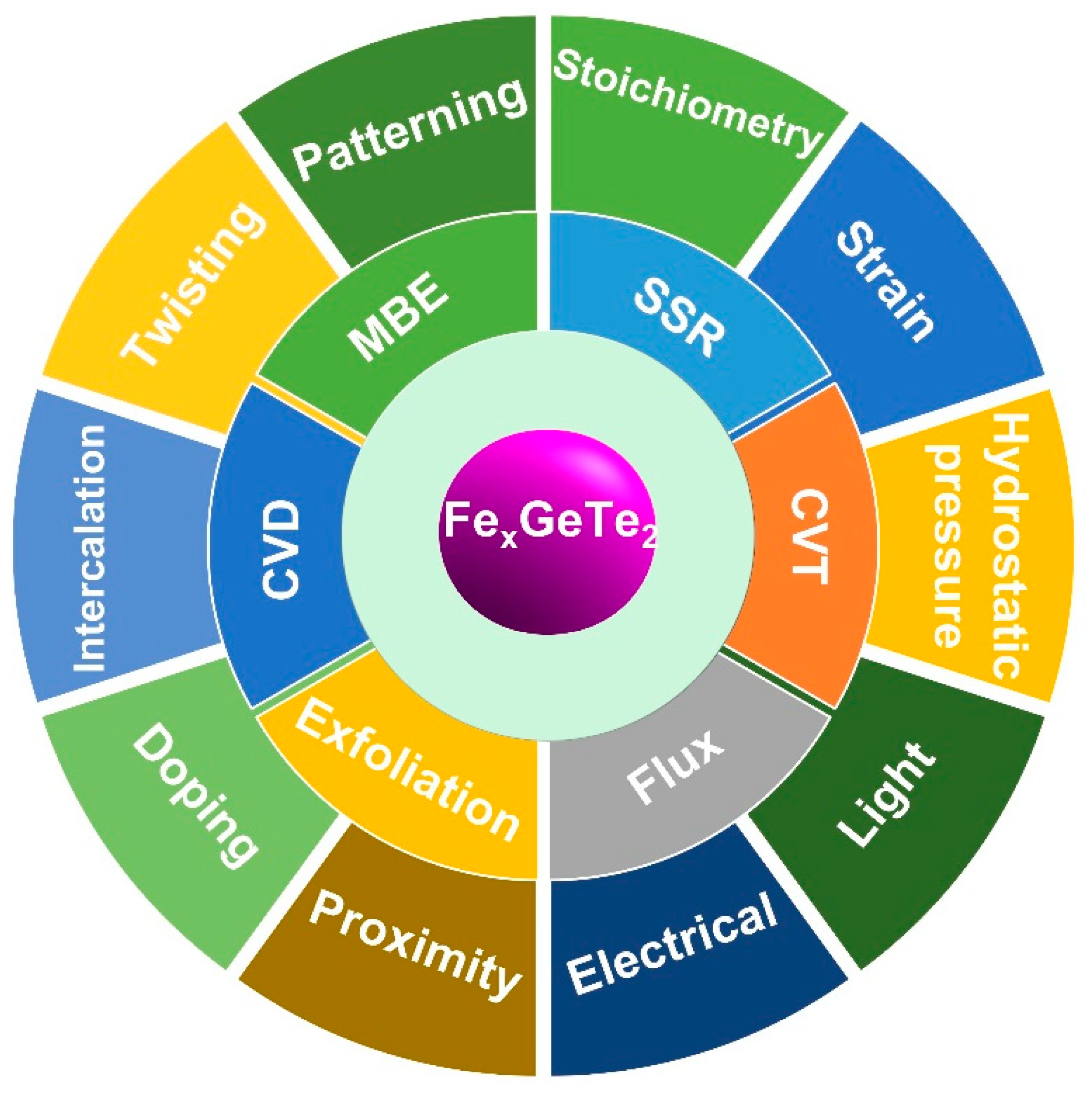
Figure 2.
Crystal structure and band structure of FexGeTe2 (3≤x≤7). (A) Crystal structure of FGT monolayer. (B) DFT-LDA calculated band structures of FGT monolayer. Electronic density of states for the Fe d states in the non-spin-polarized system in units of states/eV/Fe atom/spin of Fe3GeTe2 monolayer. This non-spin-polarized electronic structure is used to obtain the density of states at the Fermi level D(EF). Reprinted with permission from Ref.[46], Copyright 2016, American Physical Society. (C) Schematic illustration of Te-substituted Fe7Ge4 crystal and of five structures in the series FexGeTe2 (4≤x≤7). (D) Stacked plane views along the [001] direction of FexGeTe2. (E) DFT+U calculated band structures of FexGeTe2. The purple and orange lines are spin-up and spin-down bands. The Fermi level (red dashed line) is set to zero. Reprinted with permission from Ref.[62], Copyright 2022, Springer Nature.
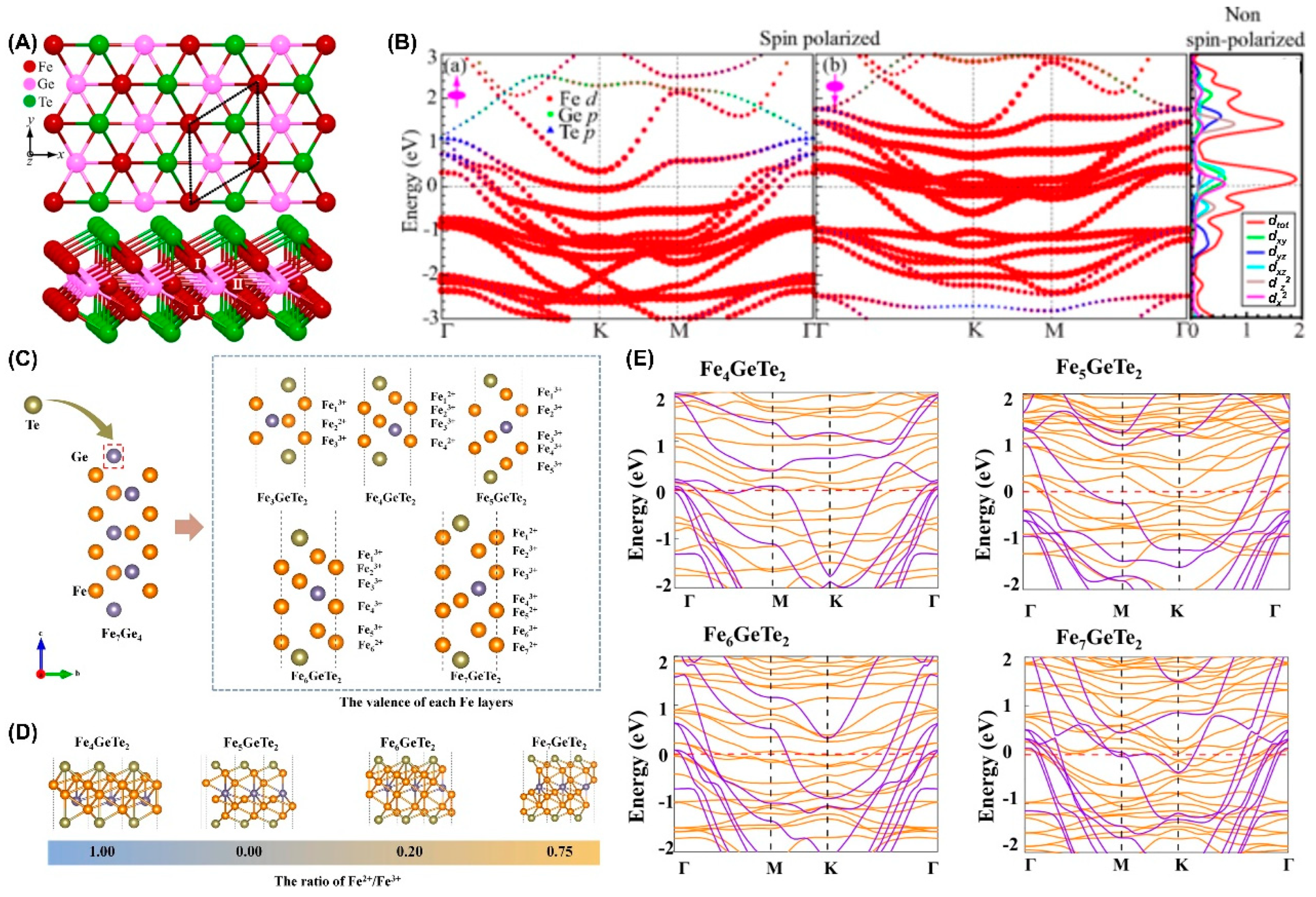
Figure 3.
SSR-prepared FGT single crystals and polycrystalline. Fe2.9GeTe2 crystal structure: (A) unit cell and (B) polyhedral representation. The Fe3 position is vacant and shown only for comparison. (C) X-ray diffraction (XRD) patterns and energy-dispersive X-ray spectroscopy (EDXS) composition maps. On the composition maps, Fe is presented in red color, Ge in green, and Te in blue. (D) Magnetic susceptibility χ versus T plot in different applied fields. Reprinted with permission from Ref. [36], Copyright 2015, American Chemical Society. (E) XRD. (F) Size distribution of the plate-like FGT single crystal. The inset is the optical photo of FGT. (G-H) Scanning electron microscope (SEM) images. Reprinted with permission from Ref.[120], Copyright 2022, American Chemical Society. (I−J) SEM images. Reprinted with permission from Ref.[106], Copyright 2019, American Chemical Society.
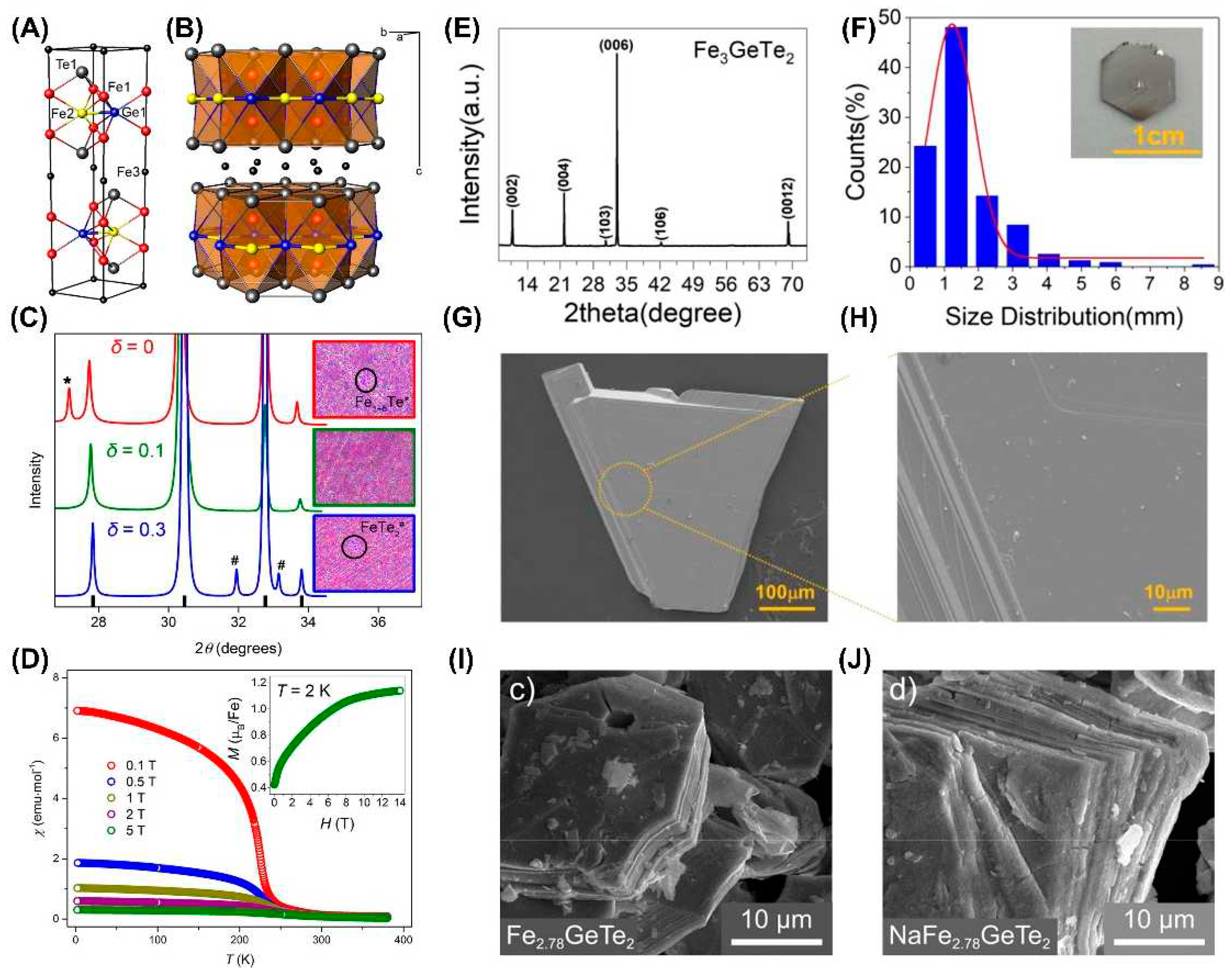
Figure 4.
CVT-prepared FGT bulk single crystals. (A) XRD. The inset shows a photograph of FGT single crystals on a 1 mm grid. Reprinted with permission from Ref.[12], Copyright 2017, American Physical Society. (B) XRD. The inset is the optical image of this FGT crystal. Reprinted with permission from Ref. [49], Copyright 2021, American Physical Society. (C) Fabrication process of the nanodevices. (D) Thickness inhomogeneity in FGT nanodevice (E). Reprinted with permission from Ref. [49], Copyright 2021, American Physical Society.
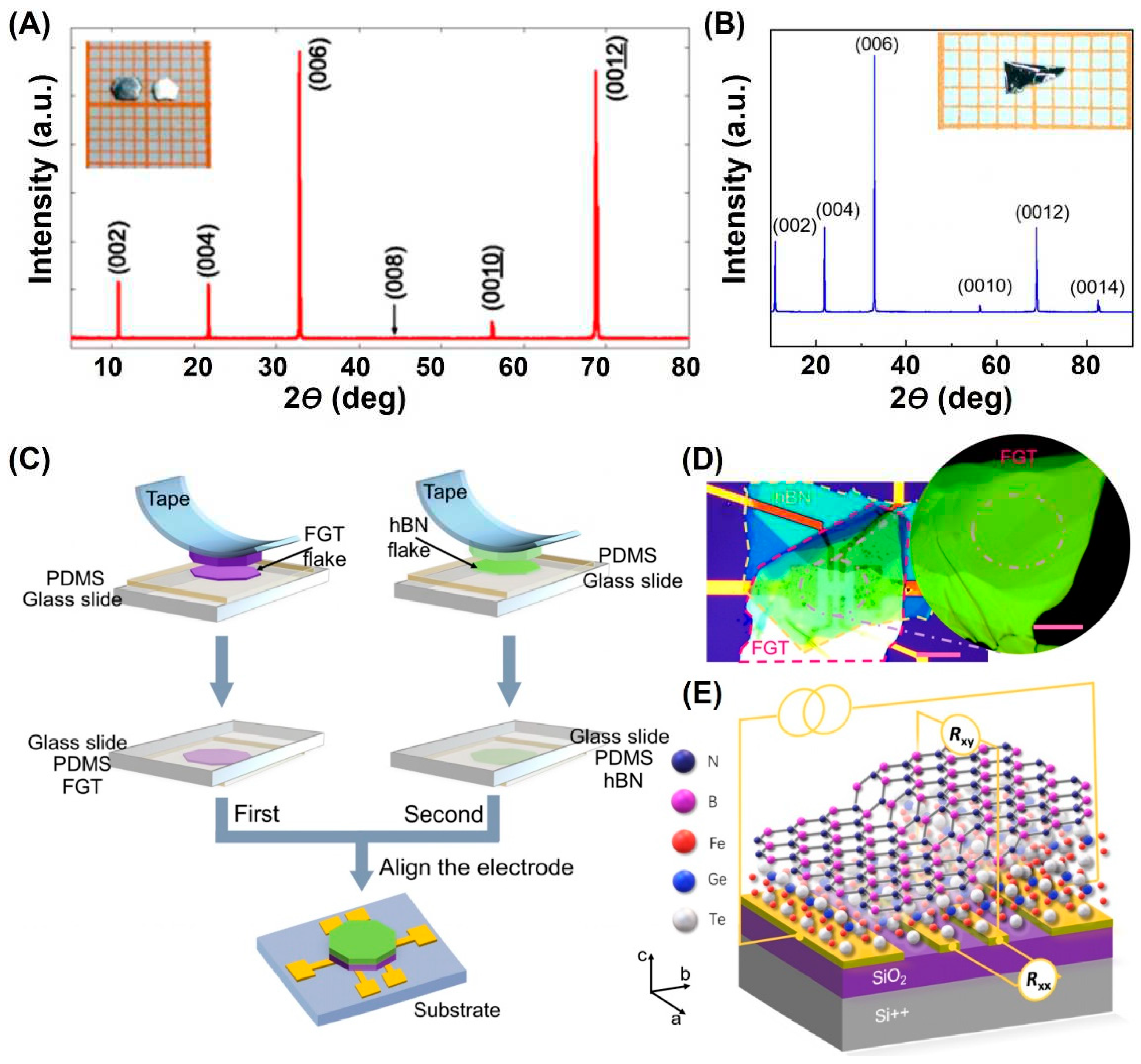
Figure 5.
FexGeTe2 single crystal prepared with self-flux. (A) A picture of a large FGT single crystal. Reprinted with permission from [9], Copyright 2016, American Physical Society. (B) Fe2.75GeTe2 single crystals. Reprinted with permission from [21], Copyright 2019, American Physical Society. (C) EDXS mapping. Secondary electron image of the crystal with mapping performed within the rectangle. Associated maps for Fe, Ge and Te, respectively. Reprinted with permission from [125], Copyright 2021, American Physical Society. (D) Schematic diagram of the flux-assisted growth process of FexGeTe2. (E) Cross-sectional structure of FGT, Fe4GeTe2 (F4GT), and Fe5GeTe2 (F5GT). (F−L) Optical images. Scale bars: 10 μm (F); 5 μm (G-L). (J−N) Optical images of FGT nanosheets grown on sapphire at 660, 670, 680, 690, and 700°C, respectively. The scale bars are 10 μm. (O) Thickness and size evolution of FGT with temperature increase. (P) Differences of thicknesses and lateral sizes using different cosolvents. (Q) Comparison of FGT under the same growth condition. Reprinted with permission from [44]. Copyright 2022, American Chemical Society.
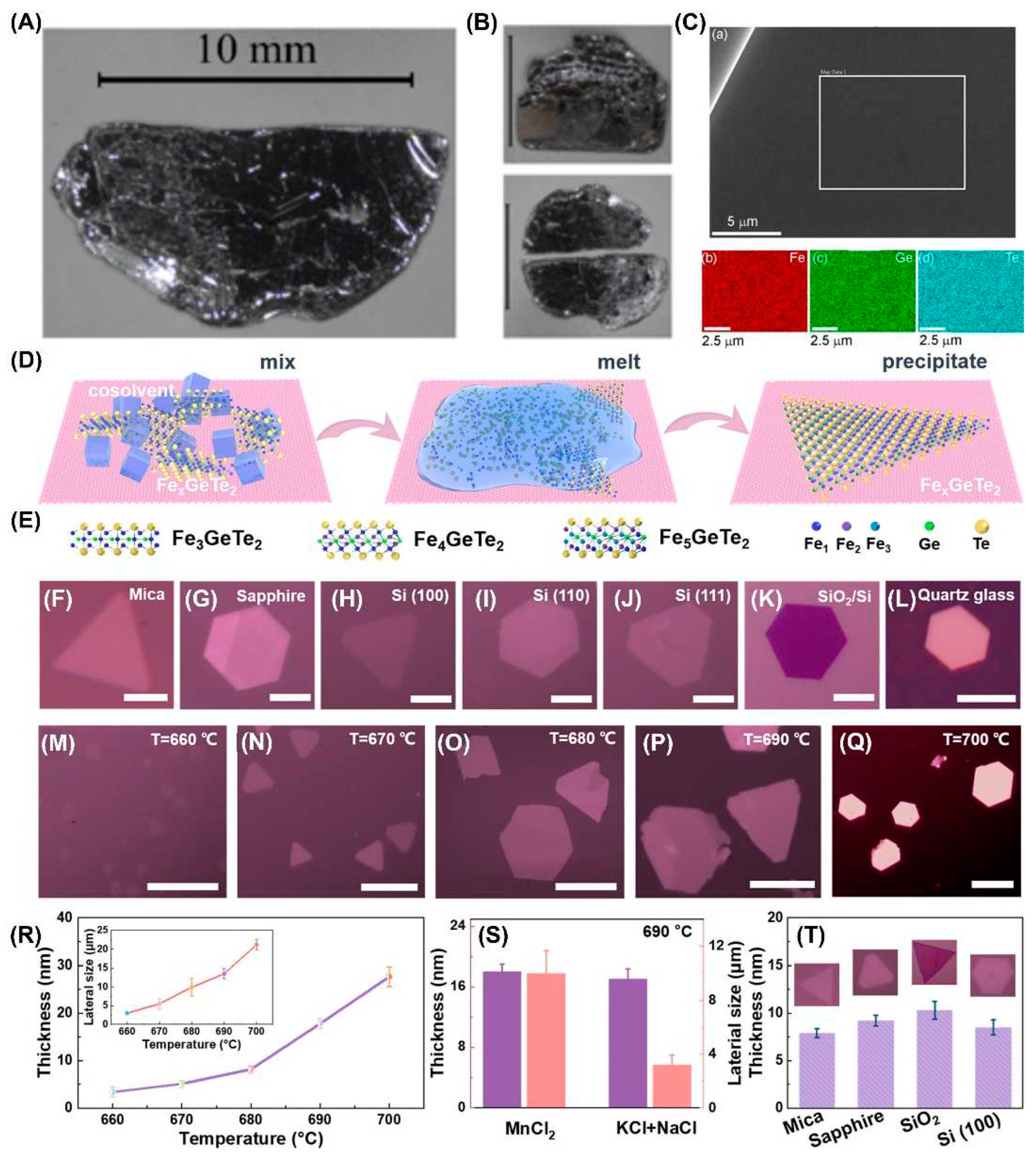
Figure 6.
(A) Schematic diagram of TS-LPE. SEM images of FGT crystals (B) in a pristine state and after ball milling (C), stirring (D), and sonication (E). (F) TEM image of FGT nanoflakes after centrifugation. (G) Statistical graph of the influence of ball-milling time on center size and the yield. (H) XRD peaks and (I) enlarged view of (002) peaks. FGT-1, FGT-2, and FGT-3 are the samples after ball milling (C), stirring (D), and sonication (E), respectively. (J) Variation of cell energy with lattice constant in the c-axis direction. (Reproduced with permission from [50]. Copyright 2022, American Chemical Society).
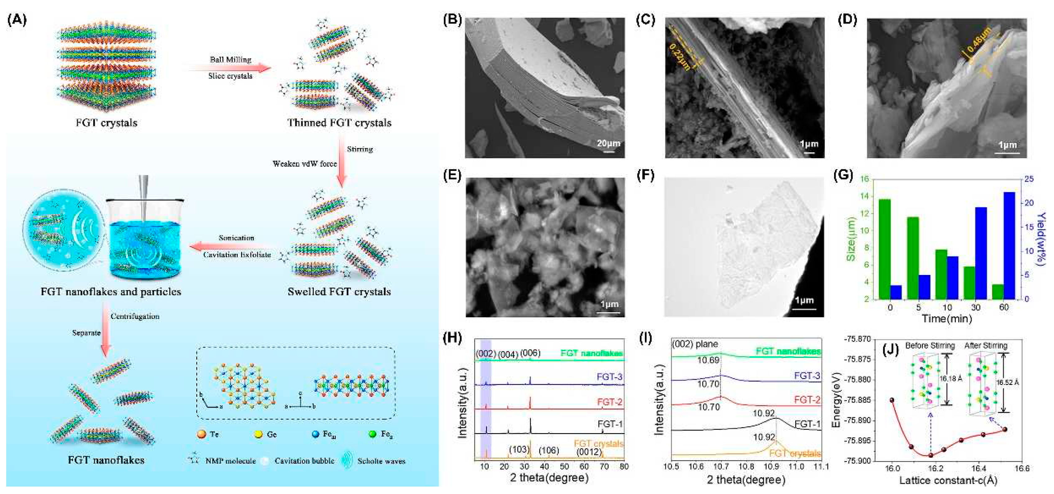
Figure 7.
MBE-prepared FGT thin films. (A) Structure geometry. (B) RHEED oscillations. The inset is the RHEED picture with streaky stripes. (C) XRD. (D) Cross-section HRTEM images. Scale bar: 2 nm. (E) Corresponding selected area electron diffraction (SAED). (F) EDS mapping results. Reproduced with permission from [7]. Copyright 2017, Springer Nature. (G) Lattice structure. (H) In situ RHEED images. (I) RHEED intensity oscillations. (J) XRD. Reproduced with permission from [55]. Copyright 2020, Springer Nature. (K) Geometric structure diagram of Bi2Te3 and FGT. The top view of FGT clearly shows the hexagonal distribution. (L) RHEED images of 8 nm Bi2Te3 and 5 nm FGT. The streaky stripes demonstrate the high-crystalline quality and 2D growth mode. (M) Atomic force microscopy images. (N) XRD. (O) Cross-section High-angle annular dark-field scanning transmission electron microscopy (HAADF-STEM) image. Scale bar: 0.5 nm. Reproduced with permission from [56]. Copyright 2020, American Chemical Society. (P) A typical HRTEM image. Reproduced with permission from [64]. Copyright 2023, Springer Nature.
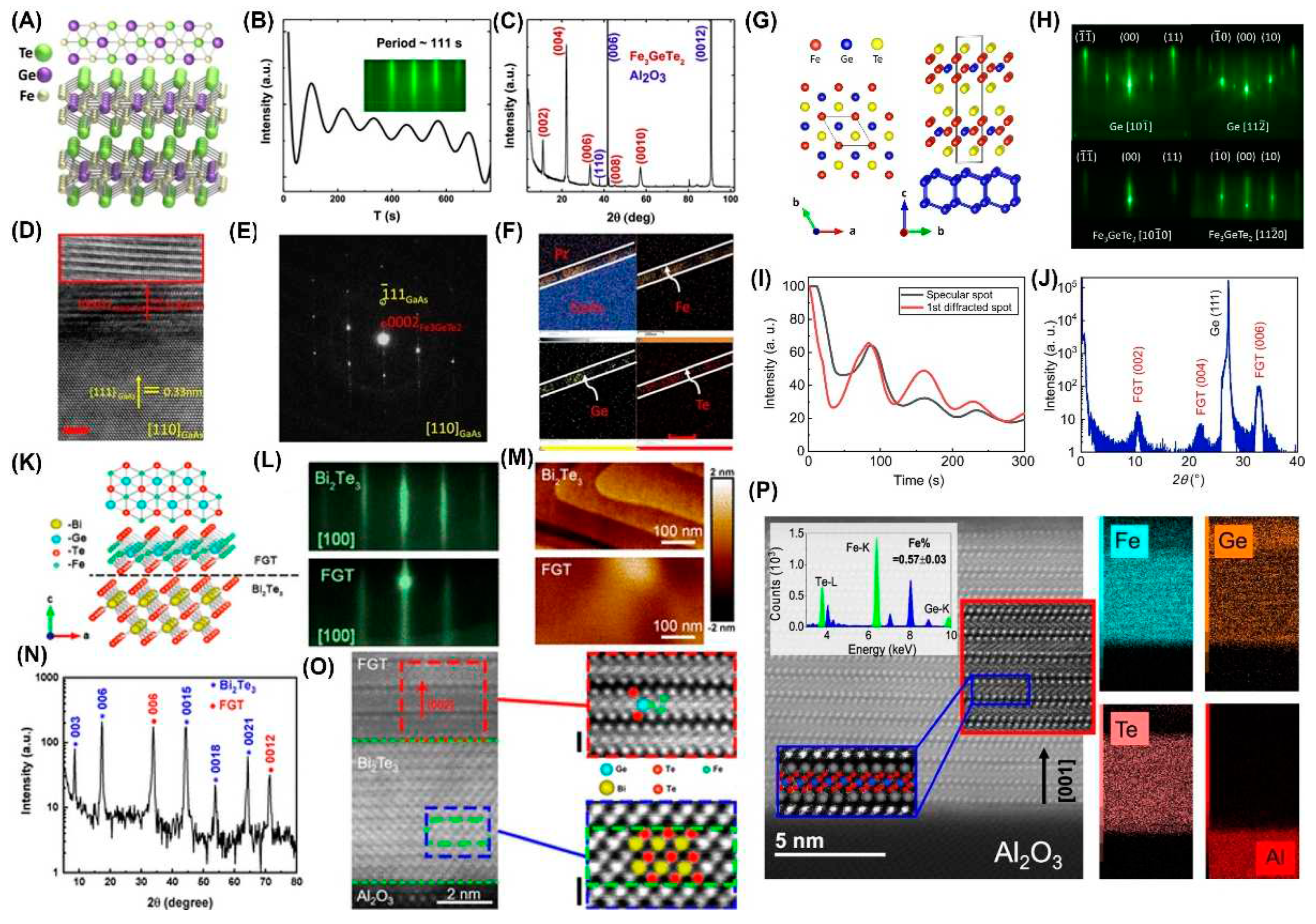
Figure 8.
(A) Normalized lattice parameters as a function of refined Fe content for FGT samples [powder x-ray diffraction (p-xrd) at room temperature], including results obtained from single-crystal x-ray (sc-xrd) diffraction data collected at 173 K. (B) TC as a function of lattice parameters. Reprinted with permission from [9], Copyright 2016, American Physical Society.
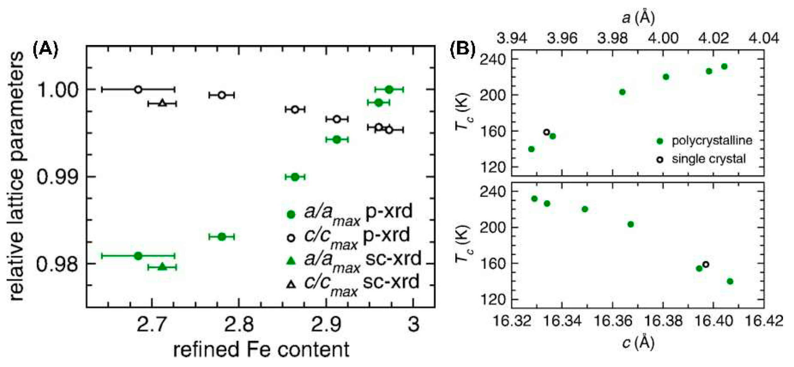
Figure 9.
(A) Calculated magnetic anisotropy energy (MAE) and magnetic moment per atom for various Fe2+/Fe3+ ratios (x). (B) Calculated normalized magnetization of Fe atoms in FenGeTe2 as a function of temperature from Monte Carlo simulation. Reprinted with permission from Ref.[62], Copyright 2022, Springer Nature. Crystal structure (C-F), the highest Jij interactions (G-J), MAE (K-N) and TC (O-R) of FexGeTe2 (3≤x≤5) monolayer. Side views of FGT (C), F4GT (D), UUU Fe5GT (E), and UDU F5GT monolayer (F). The half-colored circles in Fig. 9(F) show the Fe1-Ge split sites present in the UDU configuration. The lower panel shows 3D side view of FexGeTe2 monolayers. Note that:
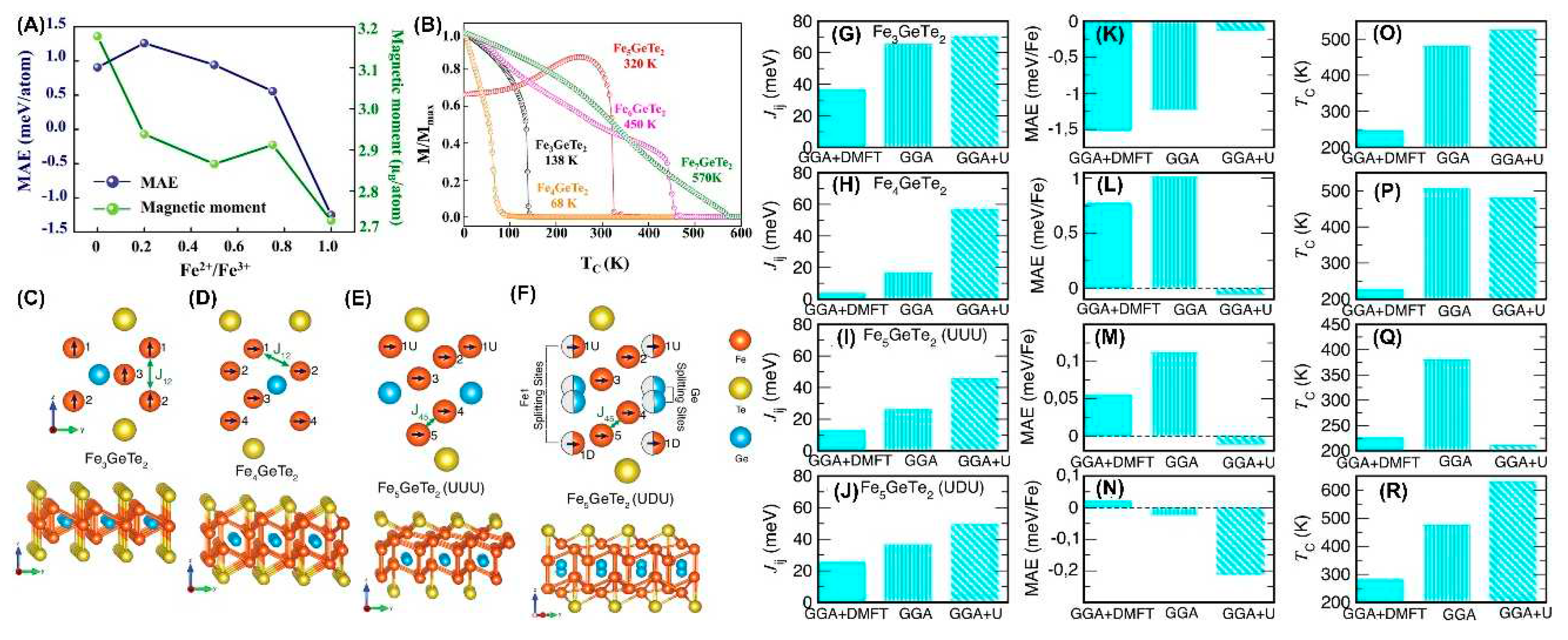
Figure 10.
(A) Schematic of lattice structure of FGT under pressure. (B) Schematic of in situ MCD experimental setup under hydrostatic pressure. The thin FGT sample was covered with a thick h BN to avoid degradation induced by pressure media. P: Polarizer; PEM: photoelastic modulator; BS: beam splitter; DAC: diamond anvil cell; LO: 50× long-working distance objective; L: lens; FGT: thin FGT sample. (C) Temperature-dependent MCD measurements. Above 163 K at 3.7 GPa and 90 K at 7.3 GPa, as indicated by the line, intermediate magnetic states appear. Then, FGT thin flake transforms to PM states above 203 K at 3.7 GPa and 163 K at 7.3 GPa, respectively. (D) MCD measurements. (E) Pressure-dependent phase diagram. The gray region represents single-domain (SD) ferromagnetic state, the yellow region represents labyrinthine-domain (LD) ferromagnet, and the pink region means paramagnetic state. Reprinted with permission from Ref.[77]. Copyright 2019, American Chemical Society. (F) Temperature dependence of the zero-field-cooling magnetization. The inset shows dM/dT as a function of temperature for different pressures. (G) The pressure dependence of Tc, where Tc is estimated from the minimum point of dM/dT. (H) The hysteresis loops were obtained at 100 K with applying pressure. The inset is an enlarged area for the details of the changes in the Ms. (I) The variation of Ms for FGT with increasing the pressure. Reprinted with permission from Ref.[78]. Copyright 2021, American Physical Society.
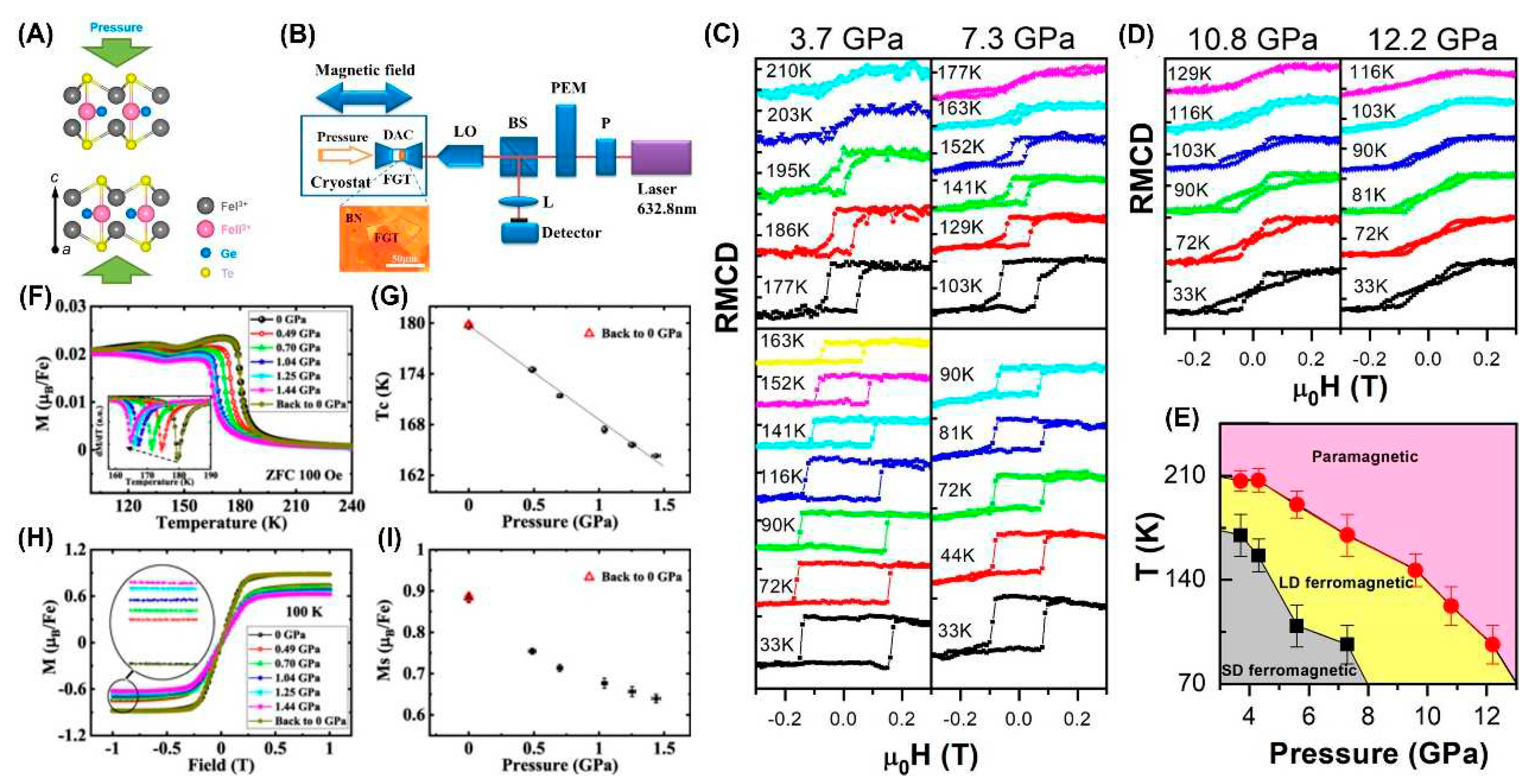
Figure 11.
(A) The atomic structure of monolayer FGT. (B) Temperature-dependent Hall resistance (Rxy) as a function of the perpendicular magnetic field. (C) Diagram of the experimental configuration for static magneto-optical kerr effect (MOKE) measurements. BS and the WS here represent the beam splitter and Wollaston splitter, respectively. (D) Schematic of the laser-excited DOS in few-layered FGT thin films. The photon energy of 3.1 eV causes electron transitions (vertical blue arrows) from occupied states below the Fermi level EF to the unoccupied states above EF. (E–G) the static magnetic hysteresis loops of seven-, four-, and two-layer thickness at different excitation intensities of the pulsed laser at RT. Reprinted with permission from Ref.[53]. Copyright 2020, American Physical Society.
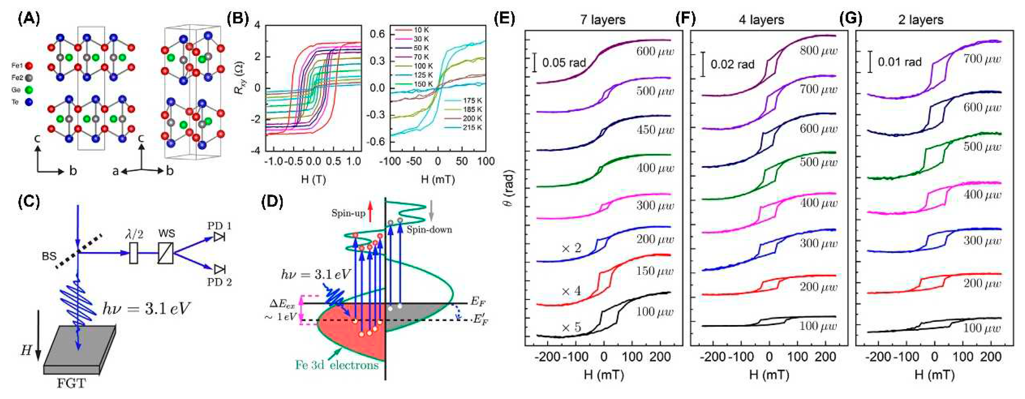
Figure 12.
Schematics of the atomic structure (A-B) of the FGT monolayer. The dual-gate configuration is shown in (B) for simulating the electrostatic gating. (C) The MAE per unit cell as a function of the charge doping concentration in the single-gate (squares) and dual-gate (dots) configurations. The results using the force theorem is denoted by the black line. Reprinted from Ref. [82] with the permission of AIP Publishing. (D) A series of dI/dV curves taken from set point of 50−1000 pA at the same position. (E−G) Calculated band structures of monolayer FGT at zero, 0.2, and 0.6 V/Å electric field, respectively. The colors show the projected Fe d orbitals. The greenlines are a guideline for the eyes, marking the band shifting under electric field. (H) Variation of MAE with the electric field. (I) Differential charge density of monolayer FGT at 0.6 V/Å electric field (relative to that at zero field). The yellow and blue colors represent the electron accumulation and depletion regions with isosurface of 0.005 e/Å3, respectively. Reprinted with permission from [83]. Copyright 2021 American Chemical Society.
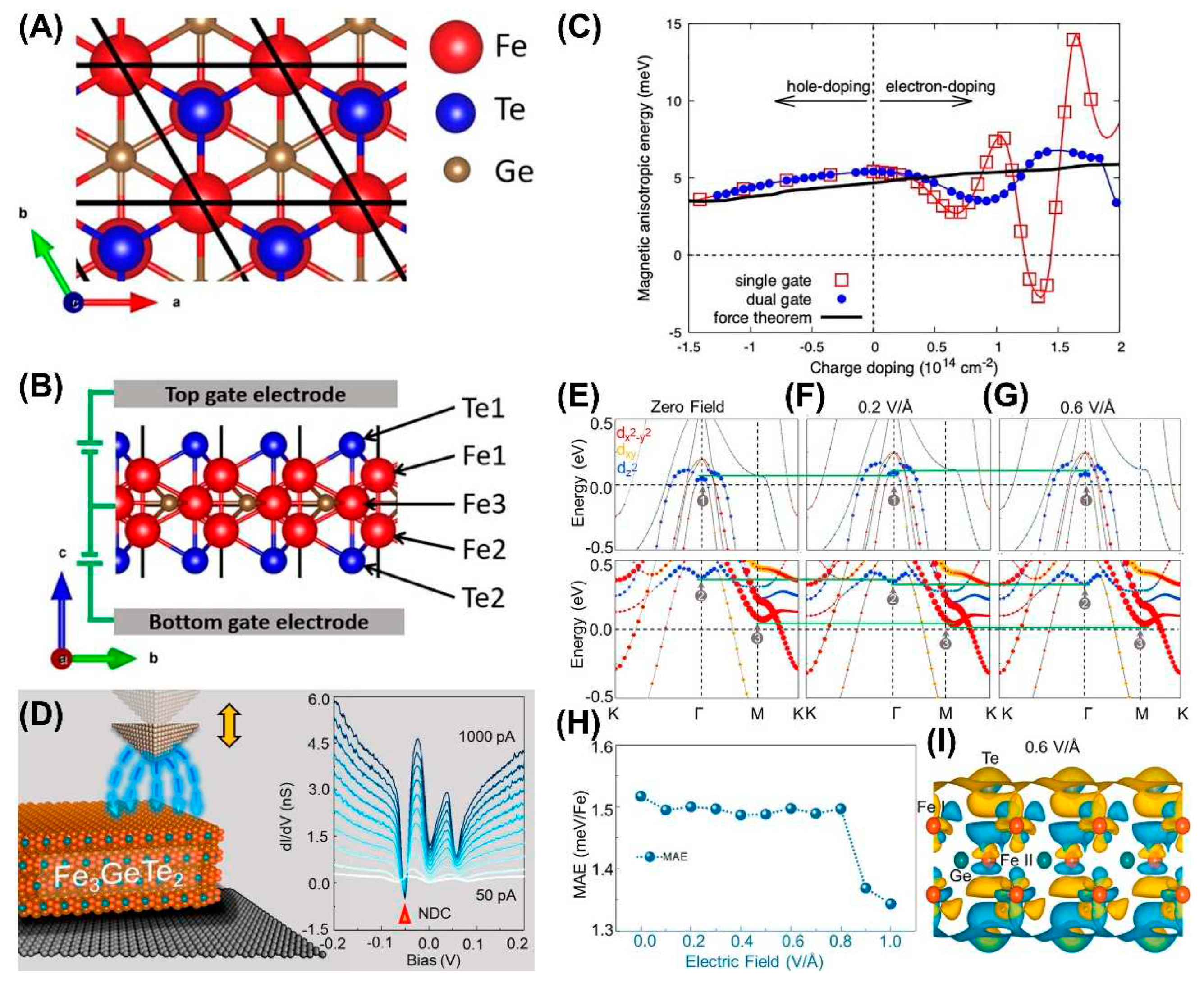
Figure 13.
The RMCD signals of FGT flakes with varying thicknesses on Au, SiO2, and Al substrates are shown in (A)–(C). The saturation fields as a function of temperature for FGT flakes with varying thicknesses on three substrates are shown in (D)–(F). The empty circles are fitted by using the function α(1-T/TC)β. The dotted line corresponds to zero RMCD signal and saturation field. (G)–(I) TC was extracted as a function of the thickness of the FGT flakes on three substrates from RMCD measurements. Reprinted from Ref. [87]. with the permission of AIP Publishing.
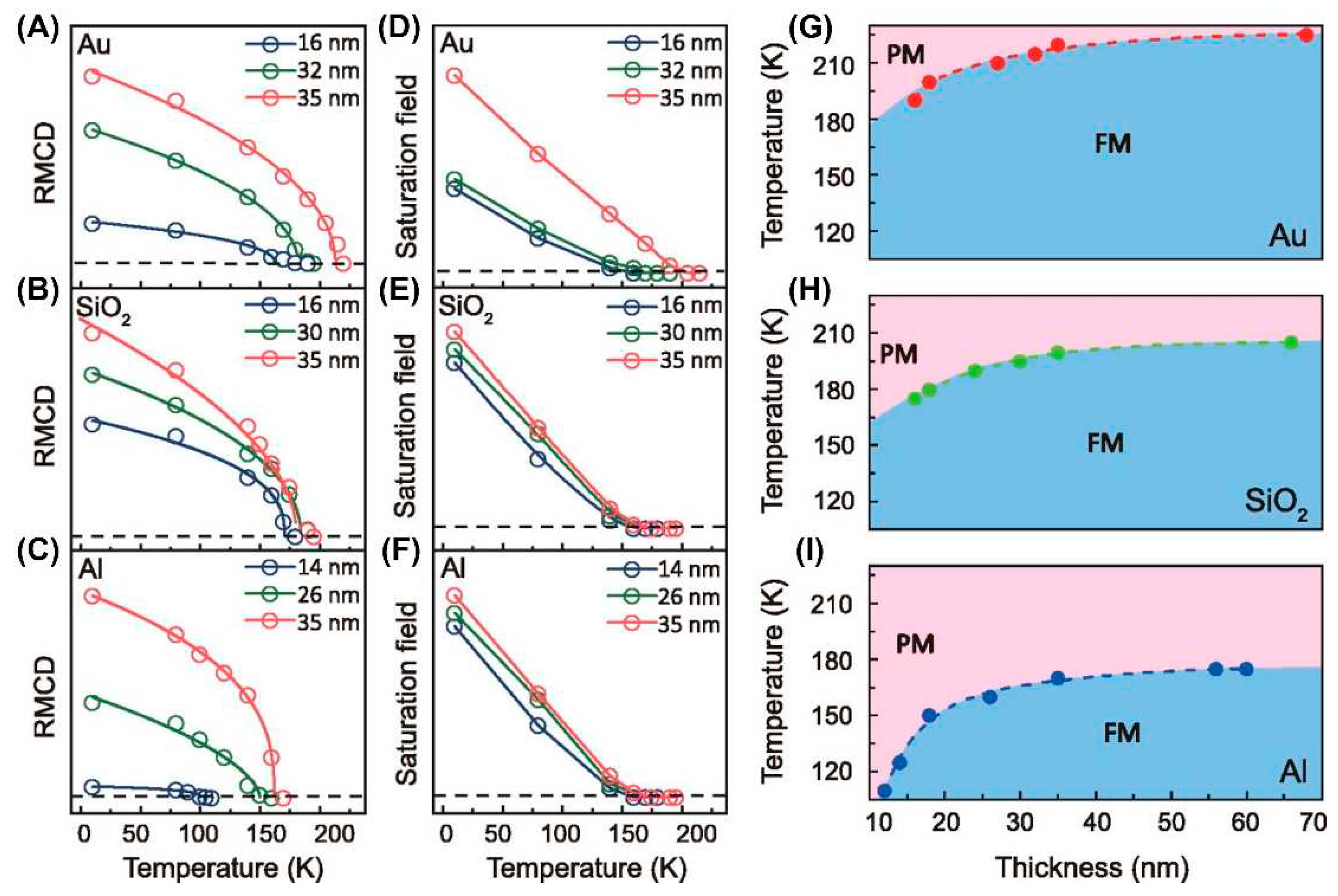
Figure 14.
M-T curves (A) and M-H loops (B) of Ni-doped FGT single crystals. (C) Phase diagram of Ni-doped FGT single crystal determined from magnetization and TF-SR (TM), and resistivity measurements (TC), showing a FM region up to x=0.3 which is smeared into a FM spin glass. Reprinted with permission from Ref.[38]. Copyright 2018, American Physical Society. (D) M-H loops of Co-doped FGT single crystals at 2 K. Doping dependent of HC (E) and MR/MS (F) values. Reprinted with permission from Ref.[92]. Copyright 2018, American Physical Society.
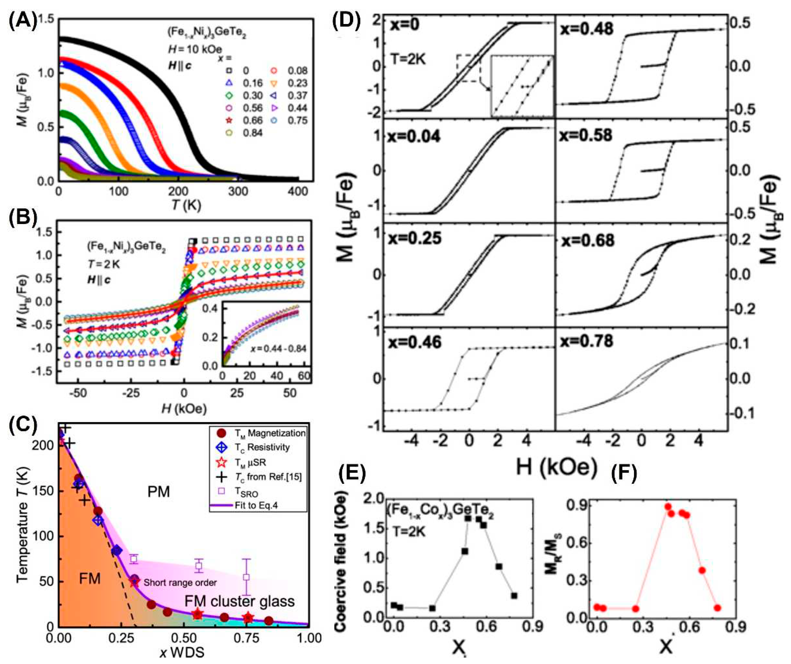
Figure 15.
(A) Schematic of F5GT layer with atomic types and positions labeled. (B) Change in lattice type (rhombohedral/primitive) with cobalt doping (gold spheres) and corresponding evolution of magnetic order and anisotropy (black arrows). (C) Experimental versus nominal cobalt concentration with shaded regions where FM and AFM behavior are observed. (D) XRD. (E) Curie and Néel temperatures, (F) magnetization induced along [001] at 300 K, and (G) saturation magnetization. The dashed vertical lines indicate the approximate region where the magnetic anisotropy inverts for the ferromagnetic compositions; the solid lines in the FM region are to facilitate viewing. The AFM region is likely characterized by FM planes that are coupled antiferromagnetically along [001]. Reprinted with permission from Ref.[94]. Copyright 2020, American Physical Society. (H) Schematic of the melt flux containing CoyFe5−yGeTe2 and the salt mixture of KCl and NaCl. OM and EDS mapping images of CoyFe5−yGeTe2 (I, K) and NiyFe5−y GeTe2 (J, L). (M) The EDS comparison of two CoyFe5−yGeTe2 samples. (N) Comparison of TC of F5GT, Co1Fe4GeTe2, and Co3Fe2GeTe2. M−H curves of Co1Fe4GeTe2 (O) and Co3Fe2GeTe2 (P). Reprinted with permission from Ref.[44]. Copyright 2022, American Chemical Society.
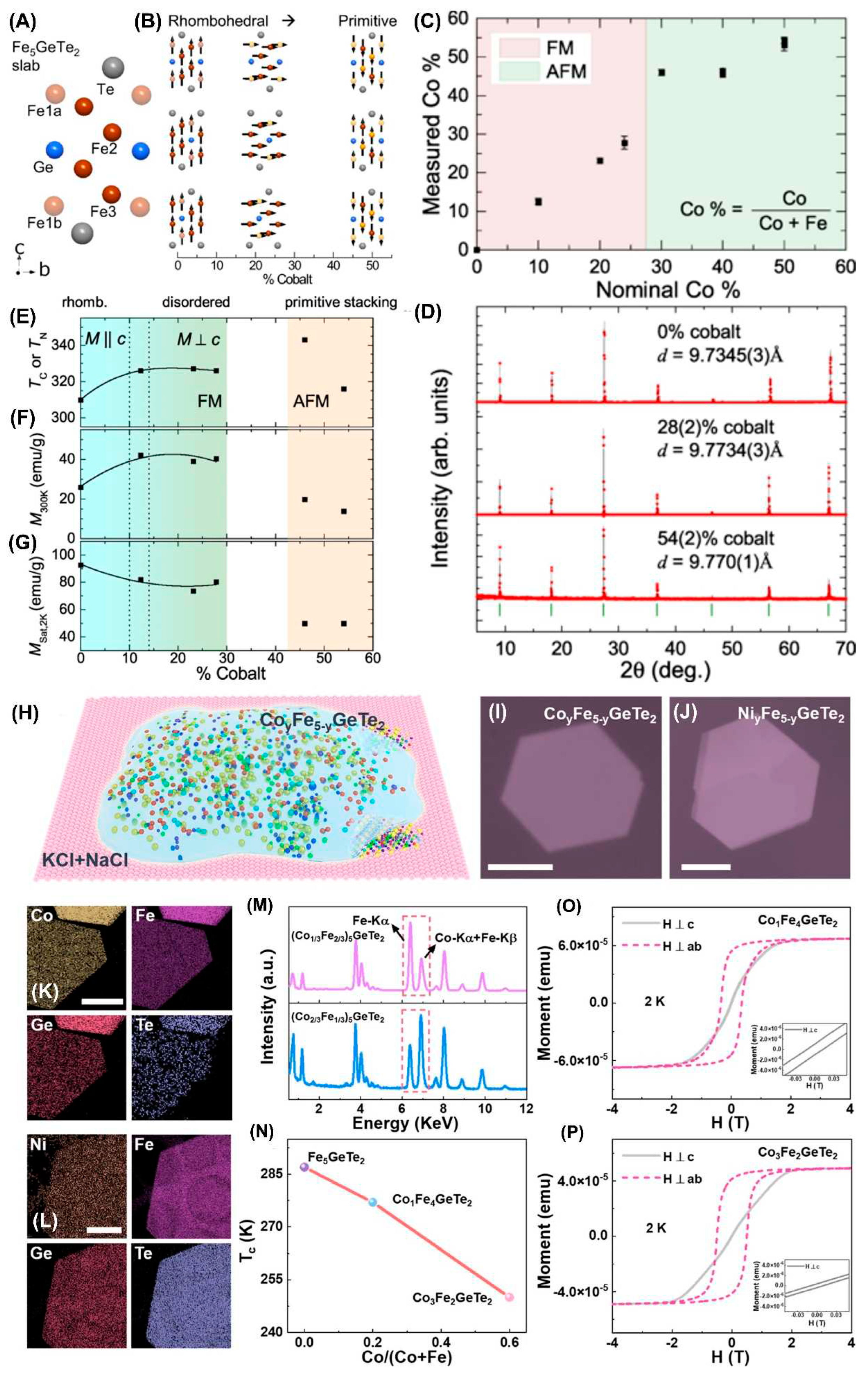
Figure 16.
(A) Schematic of the Hall-bar device on solid proton conductor used for measurements in (B) and (C) in which the current density is J and a perpendicular magnetic field B is applied. (B) Gate-tuned FM in FGT nanoflake. (C) Remnant hall resistance Rxy as a function of temperature. Inset: Schematic of possible AFM phase in pristine FGT. (D) Exchange-bias effect after zero-field cooling at 2 K. The correlation between coercivity and exchange-bias (EB) amplitude after zero-field cooling (E) and field cooling (F). (G) Schematic of differing AFM-FM interfaces. Reprinted with permission from [99], Copyright 2020, American Physical Society. Schematic diagram (H) and optical image (I) of a F5GT SP-FET, where an F5GT flake lies on the solid proton conductor (SPC). Scale bar: 10 μm. (J) ρxy loops. (K) Gate voltage-dependent carrier densities and anomalous hall ratios. PBE (L) and LDA+U (M) band structure and with corresponding hall conductivity. In parts l and m, the red lines indicate the energy bands fully located above Fermi level, while blue lines indicate the other bands. (N) Evolution of energy difference between FM and AFM (ΔE) with charge doping under LDA+U and PBE functionals. Reprinted with permission from Ref. [60]. Copyright 2021, American Chemical Society.
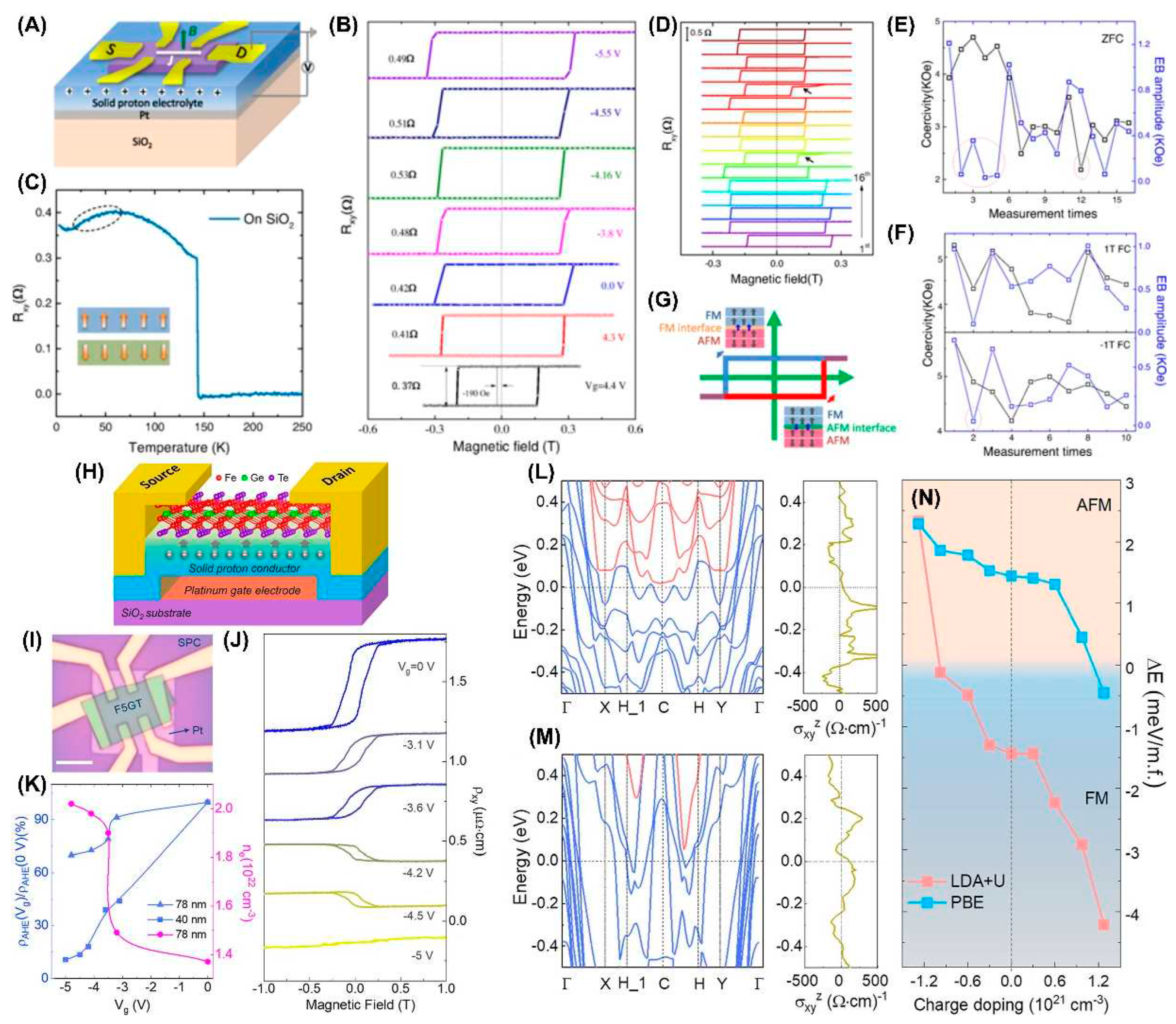
Figure 17.
(A) Optical image of a FGT flake. (B) Height profile. (C) HC of Fe deficient Fe3−xGeTe2 and FGT. (D) MAE and doping-dependent magnetization. Reprinted with permission from Ref.[43]. Copyright 2019, American Chemical Society. (E) Large-scale STM image of FGT. (F) Atom-resolved STM topography. (G) dI/dV curves. (H) Crystal structure of FGT. (I, J) Electronic structures for pristine and Fe-deficient FGT systems, respectively. The yellow, blue, pink, and green circles in (I) and (J) represents Te, Fe(I), Fe(II), and Ge atom contribution, respectively. In order to emphasize the hole doping effect in the E−k curves, the scaling factor of various atoms were changed into Te (*15), Fe I (*3), Fe II (*3), and Ge (*20). (K, L) Side views of the crystal structures for these two situations. (M, N) Illustrate the Kondo screening in a pristine Kondo lattice and in a lattice with a Kondo hole, respectively. (O, P) Real space charge density distribution and the corresponding momentum-space structures, respectively, with n(q) in (P) and the Fourier transform of the real-space distribution ni in (O). Reprinted with permission from Ref.[105]. Copyright 2021, American Chemical Society.
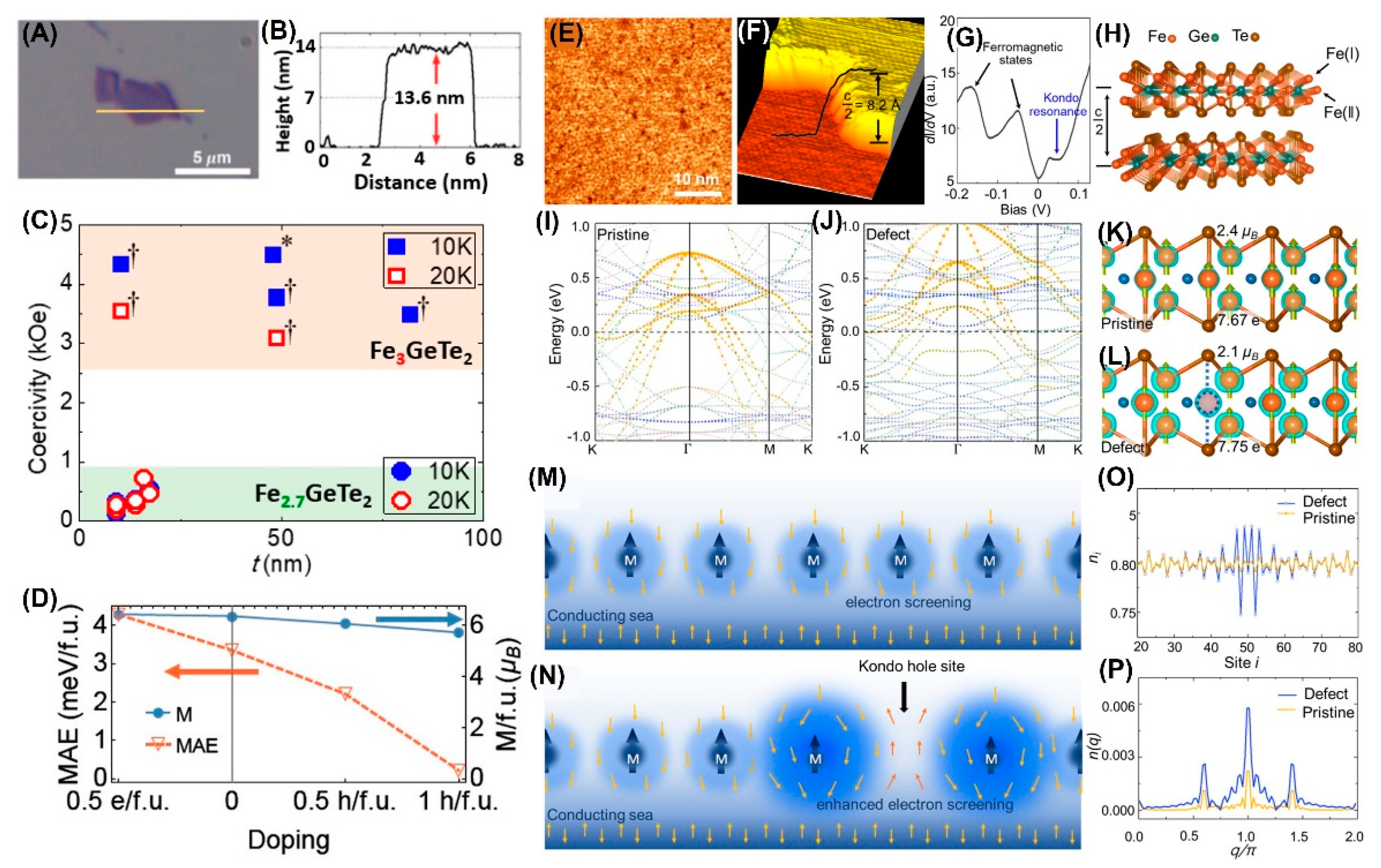
Figure 18.
(A-C) TEM image and representative SAED pattern of NaFe2.78GeTe2 as well as EDX maps of the constituting elements. (D) Temperature dependence of the specific magnetic susceptibility χg at μ0H=0.01T. (E) Field-dependent specific magnetization Mg. Reprinted with permission from Ref.[106]. Copyright 2019, American Chemical Society.
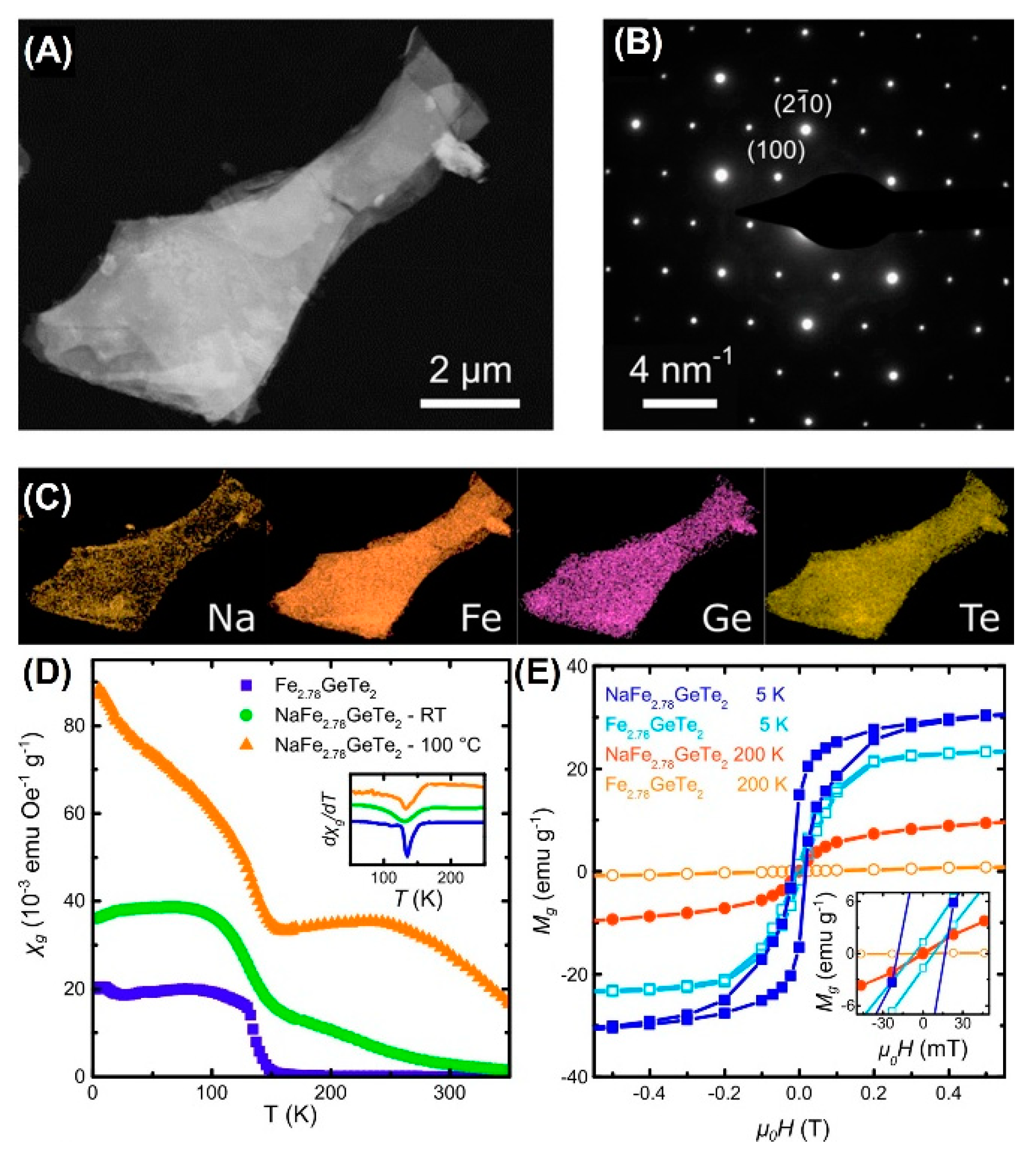
Figure 19.
(A) PEEM topography image of a FGT flake (golden color) on a silicon substrate (purple color). (B−H) Magnetic-stripe domains. (I-M) Micron-sized diamond-shaped and rectangular patterned structures. (N) Temperature dependence of the magnetic stripe contrast (out-of-plane magnetization component) and the spatially averaged contrast (in-plane magnetization component) from the two selected areas (labeled as A and B in panel N). Reprinted with permission from Ref. [16]. Copyright 2019, American Chemical Society.
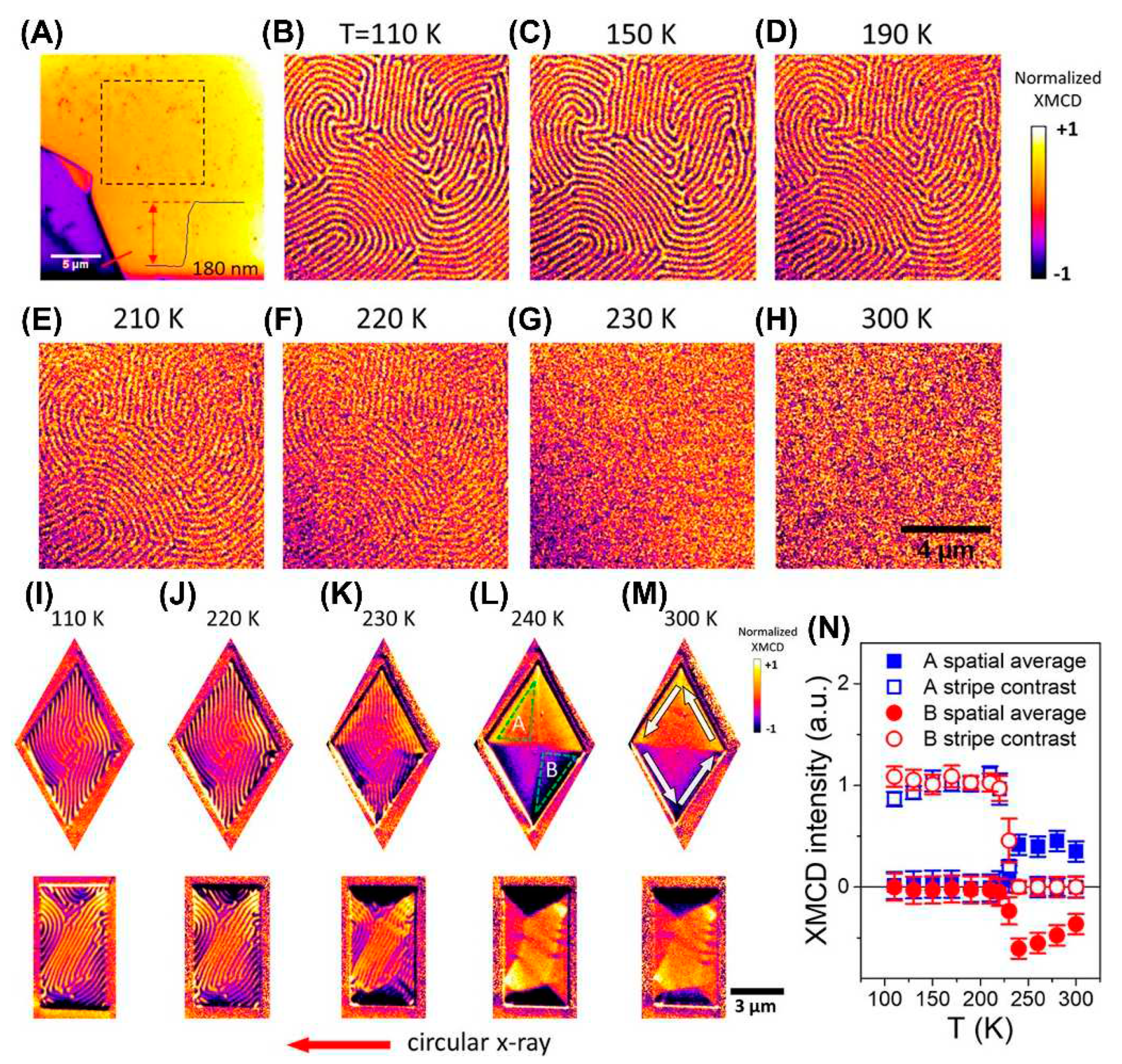
Figure 20.
(A) Schematic of an FGT/CGT/FGT MTJ and the effect of directional electric fields on charge transfer. (B) I−V curve. The inset is the optical image of this FGT/CGT/FGT MTJ. (C) Out-of-plane magnetic-field-dependent resistance, after subtracting the noise background. The gray dotted lines indicate the positions of switching fields. (D) Numerical derivative (dR/dH⊥) curves under negative V bias. Reprinted with permission from Ref.[114]. Copyright 2023, American Chemical Society. (E) Spin-valve effect in FGT/hBN/FGT van der Waals heterostructure. (F) Tunneling resistance measured at T= 4.2 K with B applied parallel to the FGT c-axis. Very sharp resistance jumps are observed for B≈±0.7 T. The variation in tunneling magnetoresistance (TMR) is ∼160%. Upper panels: zoom-in of the magnetoresistance. (G) I−V curves measured with the magnetization in the two FGT electrodes pointing parallel (black curve, B=0 T) and antiparallel (red curve, B=−0.68 T) to each other. The insets show the corresponding configuration in density of states of majority and minority spins in the two electrodes. (H) Bias dependence of TMR. Reprinted with permission from Ref.[18]. Copyright 2018, American Chemical Society.
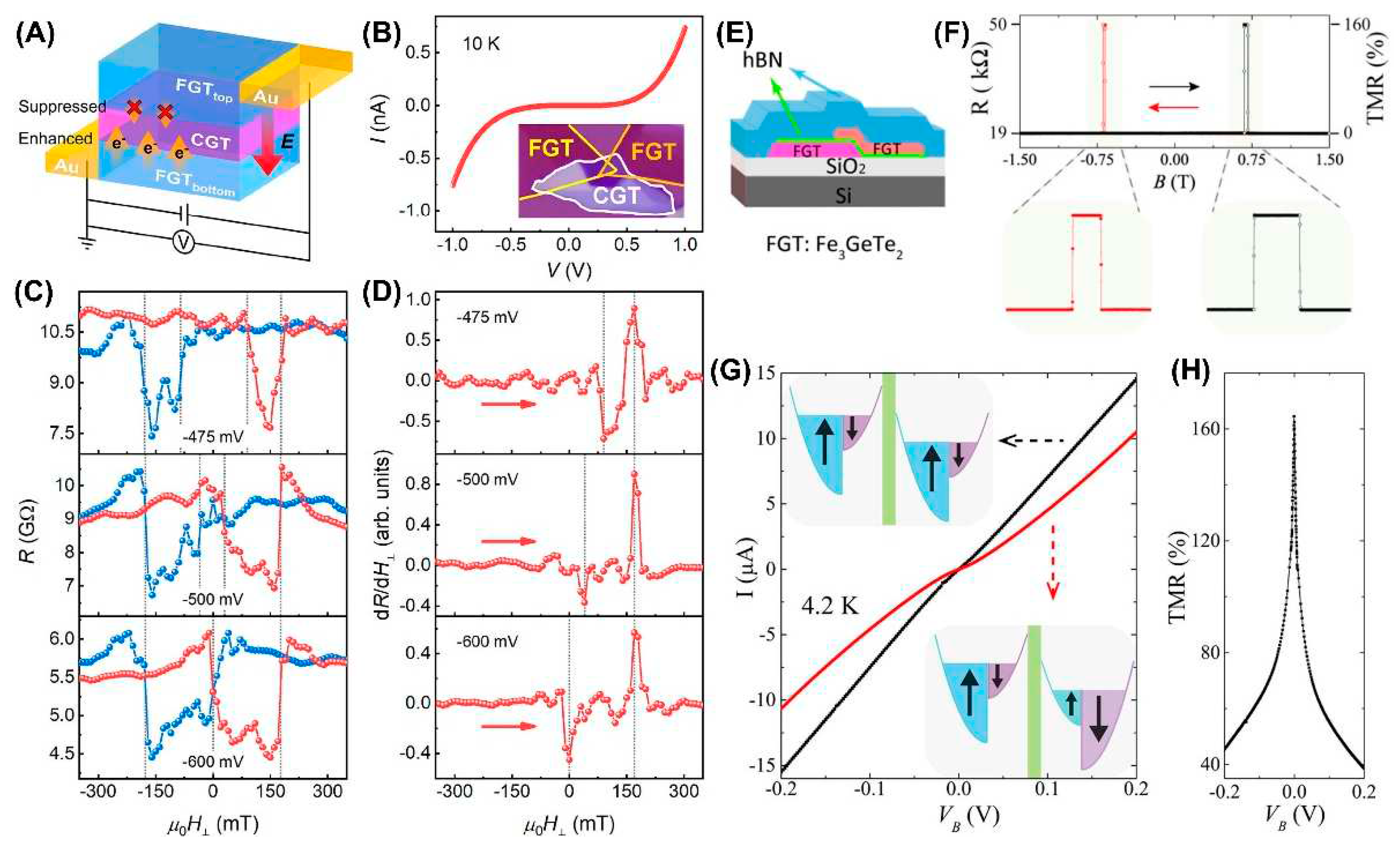
Figure 21.
(A) Schematic illustration of the effective field responsible for switching the magnetic state of FGT in FGT/Pt hybrid devices. Jx is the injected current density, Hx is the applied in-plane field, HDL is the effective field from damping-like spin−orbit torques (SOT), and M is FGT’s magnetization. (B) Hall resistance for our FGT(15 nm) /Pt(5 nm) device with anisotropy field Hk labeled on the graph. (C−F) Effective switching current as a function of applied in-plane negative, (E), and positive, (F), bias field. The color scale represents the switching resistance as a percentage of the absolute value of the anomalous Hall resistance at zero current RH0. (C,D) correspond to the line cuts in (E,F). Reprinted with permission from Ref.[20]. Copyright 2019, American Chemical Society.
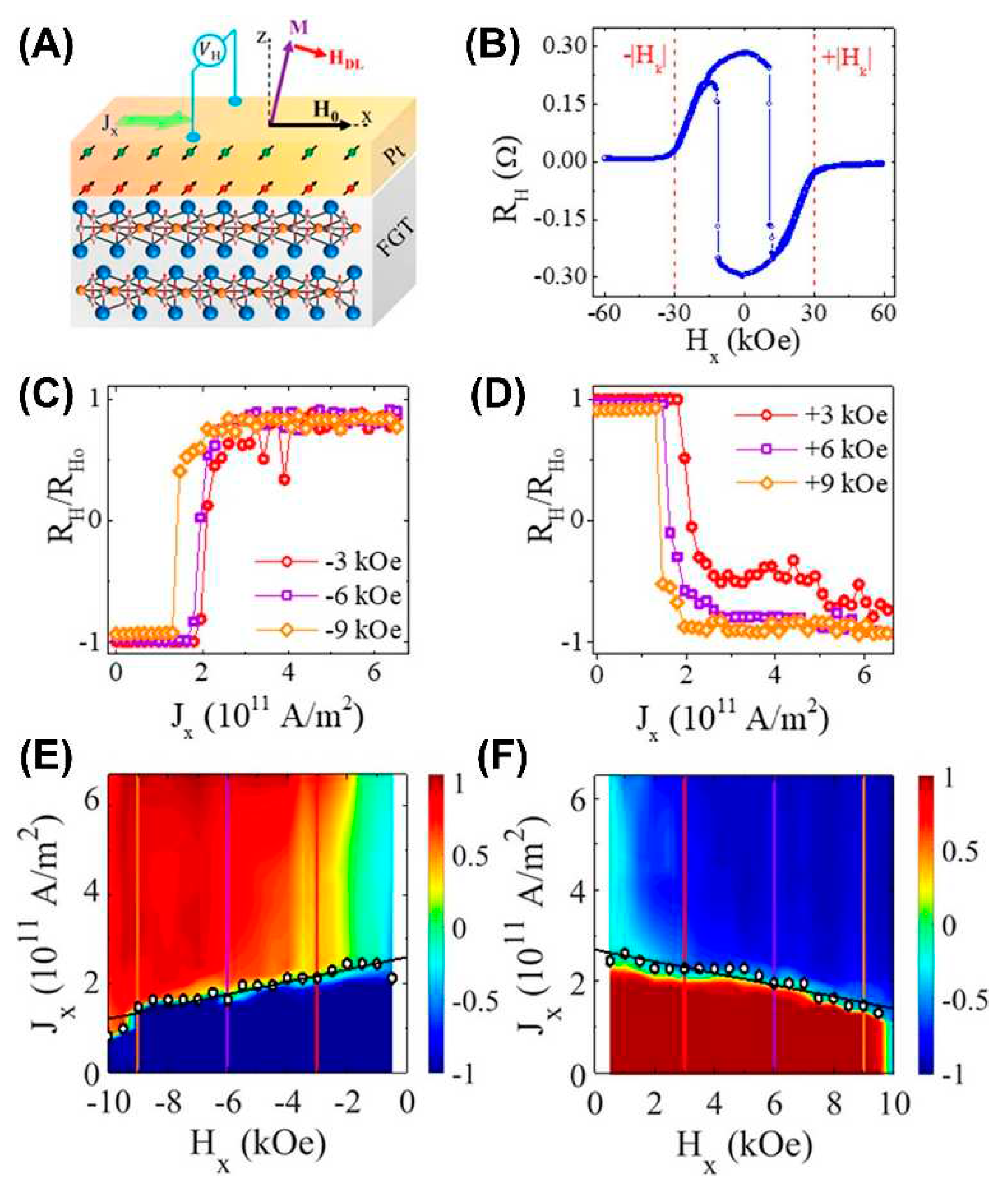
Disclaimer/Publisher’s Note: The statements, opinions and data contained in all publications are solely those of the individual author(s) and contributor(s) and not of MDPI and/or the editor(s). MDPI and/or the editor(s) disclaim responsibility for any injury to people or property resulting from any ideas, methods, instructions or products referred to in the content. |
© 2023 by the authors. Licensee MDPI, Basel, Switzerland. This article is an open access article distributed under the terms and conditions of the Creative Commons Attribution (CC BY) license (http://creativecommons.org/licenses/by/4.0/).
Copyright: This open access article is published under a Creative Commons CC BY 4.0 license, which permit the free download, distribution, and reuse, provided that the author and preprint are cited in any reuse.


