1. Introduction
The active use of sustainable energy sources such as wind and solar is a pressing need and a major challenge today. This need has been triggered epecially by environmental concerns. The typical approach is to develop energy storage devices that provide energy on demand. Numerous energy storage systems have been developed and proposed for various applications, including mechanical, electrochemical, thermal, or electrical energy storage applications. Particularly, lithium/sodium ion batteries and electrochemical supercapacitors have been widely developed as solution to store electricity because they show a very high energy storage density. Nonetheless, these electrochemical devices are prone to low power output. The ferroelectric/antiferroelectric materials are a viable option for high energy density ceramic capacitors, offering a great potential for electrostatic energy storage. In this prespective, much interest is devoted to environmentally friendly perovskites as potential candidates to replace Pb(Zr,Ti)O
3 (PZT) [
1,
2] and PMN-PT [
3], which are known for their toxicity. The use of these harmful compounds is now restricted by universal legislation such as the European Directive 2011/65/EU 2011. Among the lead-free materials of interest, Bi
0.5Na
0.5TiO
3 (BNT) has emerged as one of the most promising candidate and has witnessed an amazing research activity in recent years. This particular interest can be explained by considering the similarity between Bi
3+ and Pb
2+. Both have the stereochemically active lone electron pairs (6s
2) that are expected to contribute to the improvement of the ferroelectric and piezoelectric properties. An interesting piezoelectric coefficient of 73 pC/N with a high polarization (38 μC/cm²) and a high Curie temperature around 325°C [
4,
5] were reported in the literature for BNT ceramics. Promising properties for this compound have also been evidenced, such as an abnormal electrocaloric effect [
6] or an interesting energy storage density [
7,
8,
9].
However, BNT have also some disadvantages such as a large coercive field (Ec = 73 kV/cm) and, most importantly, high leakage currents [
10,
11,
12]. In fact, these disadvantages can be ascribed in part to the defect chemistry in BNT, which is related to different mechanisms. Bi vacancies may form due to the volatility of bismuth oxide, which induces the formation of oxygen vacancies for compensation. Volatility of Na
2O is also expected and can induce A-vacancy.
Moreover, the A site of the BNT compound contains Na
+ and Bi
3+ with close ionic radii [r(Na
+) = 1.18 Å, r(Bi
3+) = 1.17 Å] [
13] but the charge difference between these two cations favors their disordered arrangement in the matrix. Thenceforth, a plethora of works reported difficulties to polarize bismuth sodium titanate ceramics due to the high electrical conductivity [
14]. Therefore, efforts have been directed towards the fabrication of thin films. In this context, the growth of BNT thin films by various techniques has been reported [
15,
16,
17,
18]. Successful epitaxial layers have been reported in various works using different substrates and/or buffer layers [
18,
19], but single-phase BNTs could only be obtained with certain stoichiometries, for example using Bi- and/or Na
+-rich targets or Manganese in the Ti-sites when PLD is used.
On the other hand, chemical solution deposition (CSD) has shown a high degree of control over the stoichiometry and the microstructure for the synthesis of BNT thin films. For instance, Abou Dargham et al. [
18] reported that BNT films prepared by chemical solution deposition (CSD) and annealed under air atmosphere at 650°C exhibited low crystallization, while when annealed at 700 °C they exhibited good crystallization without preferential orientation or secondary phases. The authors evidenced encouraging electrical properties, but only a leaky PE hysteresis loop was achieved without reaching saturation. However, Zannen et al. [
20] reported that an air annealing of the polycrystalline BNT film at 700 °C during 5 min in a preheated tube furnace was more appropriate to obtain crack-free films with a closely saturated PE hysteresis loop under a high applied electric field. Furthermore, Hiroshi Maiwa et al. [
21] annealed under air their CSD thick films in an infrared furnace at 550-700 °C for 10 min and found comparable ferroelectric hysteresis to Zannen et al. From these previous works, it appears that the processing conditions play a crucial role in the microstructural and electrical properties of the obtained BNT thin films, and hence may explain the spread of the reported electrical properties. It is worth noting that a review of the extensive literature shows that a systematic analysis of the annealing atmosphere effect on the defect chemistry of BNT films and their associated electrical properties is lacking. Recall that a solid state dielectric capacitor enables to store electrical energy directly without any conversion. Initially in a dielectric material, dipoles are randomly aligned and while applying an external electric field (E), these dipoles are polarized and aligned in E direction. Noting that capacitor affords high power density compared to the batteries, and ultrafast charge-discharge performances compatible with high-power/pulsed-power applications. Nevertheless, the associate energy density is still very small. Shaping a dielectric material with improved energy storage properties becomes the challenge to meet the need of modern applications. There has been a lot of work done on this hot topic and it is still ongoing. In order to enrich this debate and to make a useful contribution that could be of interest to the scientific community dealing with BNT, we investigate in the present work the effect of the oxygen annealing atmosphere on the microstructure, structural and electrical properties of BNT thin film processed by Sol-gel under oxygen atmosphere. It is shown that the electrical properties are highly influenced by annealing the film under O
2. Low dielectric losses and well hysteresis loop were obtained; whereby interesting electrostatic energy storage properties could be achieved.
2. Materials and methods
BNT thin film was prepared via chemical solution deposition combining sol-gel process and spin-coating method. The precursor solution was prepared using high-purity bismuth acetate (III) (C6H9BiO6, ≥99.99%, Sigma Aldrich), sodium acetate Anhydrous (C2H3NaO2, Sigma Aldrich) and titanium isopropoxide (C12H28O4Ti; 97+% Alfa Aesar). To yield a solution with concentration of 0.3 mol/l, appropriate amounts of the reagents were dissolved in acetic acid (CH3COOH), 2-Methoxyethanol (CH3OCH2CH2OH), and acetyl acetone (AcAc, Merk Germany), which was selected as stabilizers. In a first step, Bi- and Na- acetates were dissolved in acetic acid. However, Ti- isopropoxide was dissolved in 2-methoxyethanol with the addition of the chelating agent (AcAc). The two solutions were mixed together and stirred at room temperature for 24 h until getting a stable yellow solution. The solution was spin-coated onto Pt /SiN substrate at a speed of 2000 rpm for 35 s. Noting that the substrate was subjected to a cleaning procedure, firstly in ethanol and then in deionized water ultrasonic bath, in order to remove the surface adsorbents and enabling a uniform film growth on it. Five coating sequences were performed and each layer was dried at 120°C and then pyrolyzed at 400°C during 10 min on a hotplate, respectively. Final annealing was performed at 600 °C in a tube furnace under O2 atmosphere for 30 min.
The microstructure of the investigated film was analyzed by scanning electron microscope (SEM) (Environmental Quanta 200 FEG, FEI) coupled with energy-dispersive X-ray spectroscopy (EDX). The surface morphology was studied by atomic force microscopy (AFM) using a commercial setup NTEGRA Aura (NT-MDT) microscope working in contact mode.
The identification of the purity of the phase formation was carried out by X-ray diffraction (XRD) using a four-circle high resolution Bruker Discover D8 diffractometer (D8 Advance, Bruker, Germany) operating at at 40 kV and 40 mA, equipped with a copper anticathode. A Göbel mirror yield a diffracted parallel beam and a LynxEye detector can be used in the 1D mode resulting in much shorter measurement times and better counting statistics. A beam attenuator is inserted in the incident X-ray beam. XRD investigations were carried out in both out-of-plane mode and grazing incidence mode (GIXRD). For GIXRD experiments, collimation was achieved by placing two divergence slits (0.2 mm and 0.1 mm) in the incidence path. A 0.2° equatorial Soller slit was used to limit the axial divergence of the diffracted X-ray beam. A Kβ nickel filter was mounted in the secondary path. The scans were collected with a grazing incidence angle of 2°, a 2 theta increment of 0.02° and a step time of 1 second. For out-of-plane measurements, a double reflection channel-cut Ge monochromator was used to select the Cu Kα1 radiation (1.5406 Å). A divergence slit (0.2 mm) was placed in the incident X-ray beam. The omega/2 theta scans were recorded with a step size of 0.01° and a step time of 1 second.
Raman spectroscopy was performed using a micro-Raman Renishaw spectrometer (green laser excitation of 514.5 nm) and the spectrum was collected in a back-scattering geometry. The laser power was kept below 20 mW to avoid sample heating. For electrical characterizations, top Au electrodes with 220 µm of diameter were deposited by sputtering method (Bal-Tec SCD-050) using a shadow mask. Noting that a corner of the Pt bottom electrode was left uncoated for ensuring the electrical contact. Room temperature dielectric measurements were carried out using a Solartron Impedance analyzer SI-1260 at driving signal amplitude of 25 mV and in the frequency range from 1 kHz to 1 MHz. Ferroelectric test system (TF Analyzer 3000, aix-ACCT) was used to collect P-E hysteresis loops at room temperature under different applied electric fields. A probe system attached to a Keithley 2611A source was used to measure the leakage current properties in the step mode with a delay time from 30 to 200 s to allow sample discharging.
3. Results and discussion
3.1. Microstructural analysis
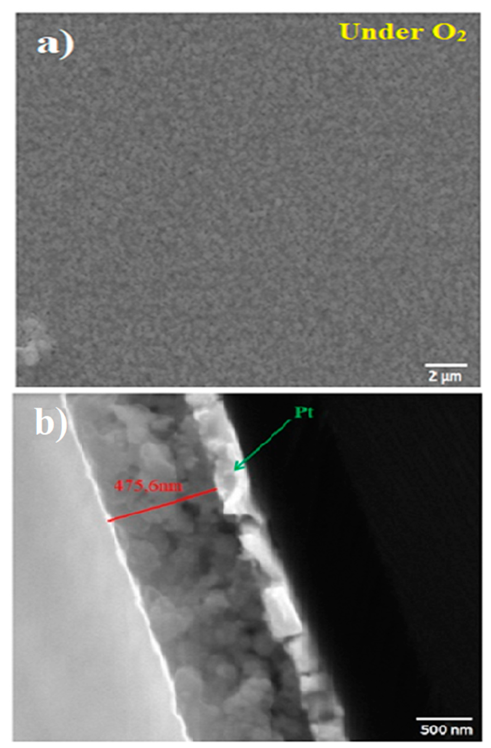
Scanning electron microscopy (SEM) micrographs of thin BNT films annealed at 600 °C under O
2 atmosphere are shown in
Figure 1. It is worth noting that the film exhibits a relatively dense grained structure without porosity and cracks. In addition, grains seem to be uniformly distributed (Fig.1a). The obtained microstructure is different to that one reported by Yang et al. [
22] for Na
0.51Bi
0.50(Ti
0.96W
0.01Ni
0.03)O
3 thin films. The authors showed that the microstructure is governed by Na nonstoichiometry. However, it is in good agreement with typical microstructure reported in the literature for BNT thin films prepared by CSD [
7]. A typical cross-section of the film is presented in Fig. 1b. It evidences a uniform thickness of about 475.6 nm.
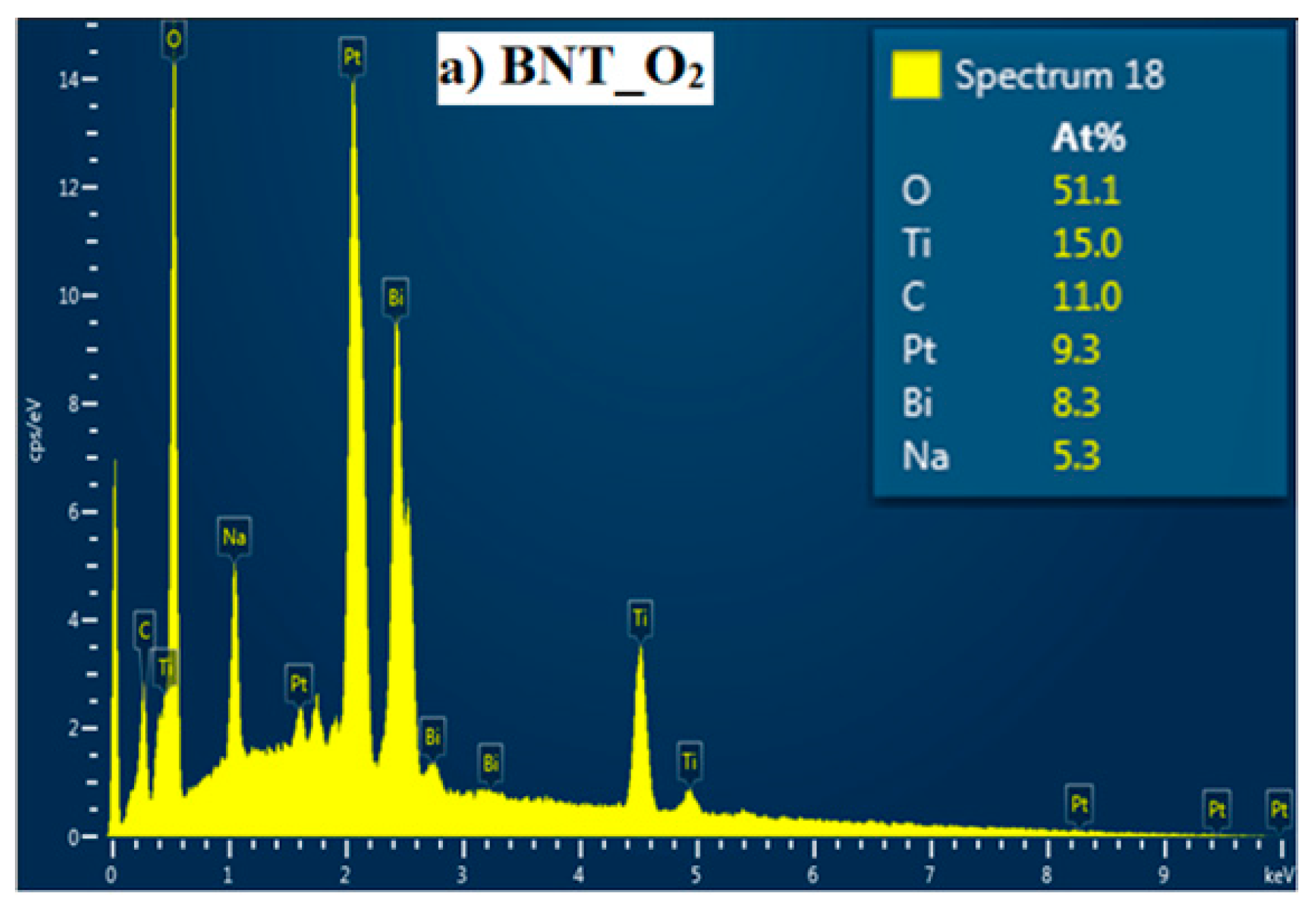
Figure 2 presents the EDX spectra in compositional distribution for the investigated BNT films. As expected, characteristics of starting elements, namely Bi, Na, Ti and O, are detected. A close look to the obtained atomic weight reveals that the BNT films show a ratio of Bi/ Na less than 1.0, thus it evidences a deficiency of Na atoms on the A site of the BNT structure.
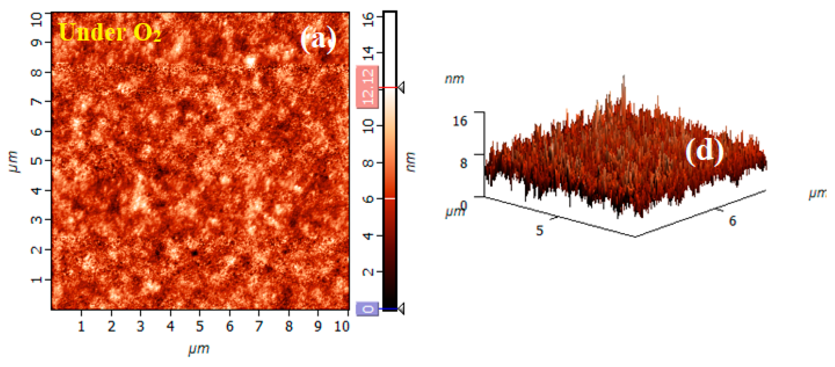
The surface topography and roughness investigated by AFM provide more insight into the understanding of the microstructure. The topography of the film surface obtained in contact mode AFM is shown in
Figure 3. The image was recorded on the 10 × 10 µm
2 scan region. A fine-grained structure is observed for the investigated sample which is essentially smooth. The founded root mean square (RMS) roughness value was 1.5 nm.
3.2. Structural investigations
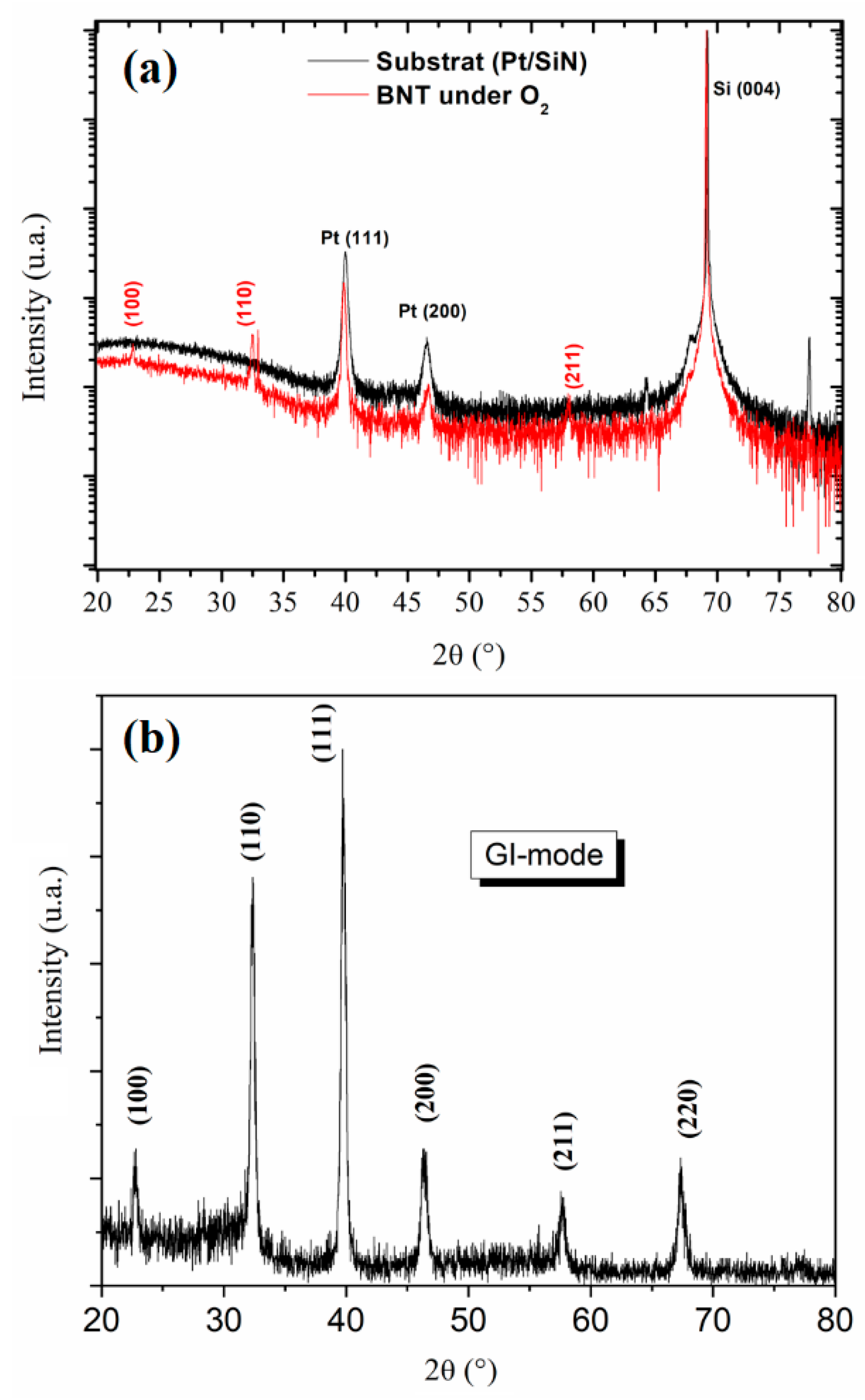
The ϴ – 2ϴ XRD patterns of the investigated sample is shown in
Figure 4. The diffractograms of BNT-O
2 and of the substrate are compared in the
Figure 4a. Several peaks of the substrate can in fact mask those of the film. Thus, the grazing incidence mode (GI) was used to eliminate the substrate contribution, and the obtained XRD patterns are presented in
Figure 4b. Noting that the film exhibits pure perovskite without secondary phase (in the limit of the diffractometer detection). The obtained diffraction peaks are indexed according to a pseudo cubic unit cell. The obtained diffractogram evidences a fully random orientation and exhibits 5 diffraction peaks in the 2θ range between 20° and 80°. These peaks appeared at 2θ = 22.69 °, 32.27 °, 39.7 °, 46.31 °, 57.57 ° and 67.31°, corresponding respectively to the (100), (110), (111), (200), (211) and (220), reflections of BNT bulk material crystallize in rhombohedral symmetry with R3c as a space group.
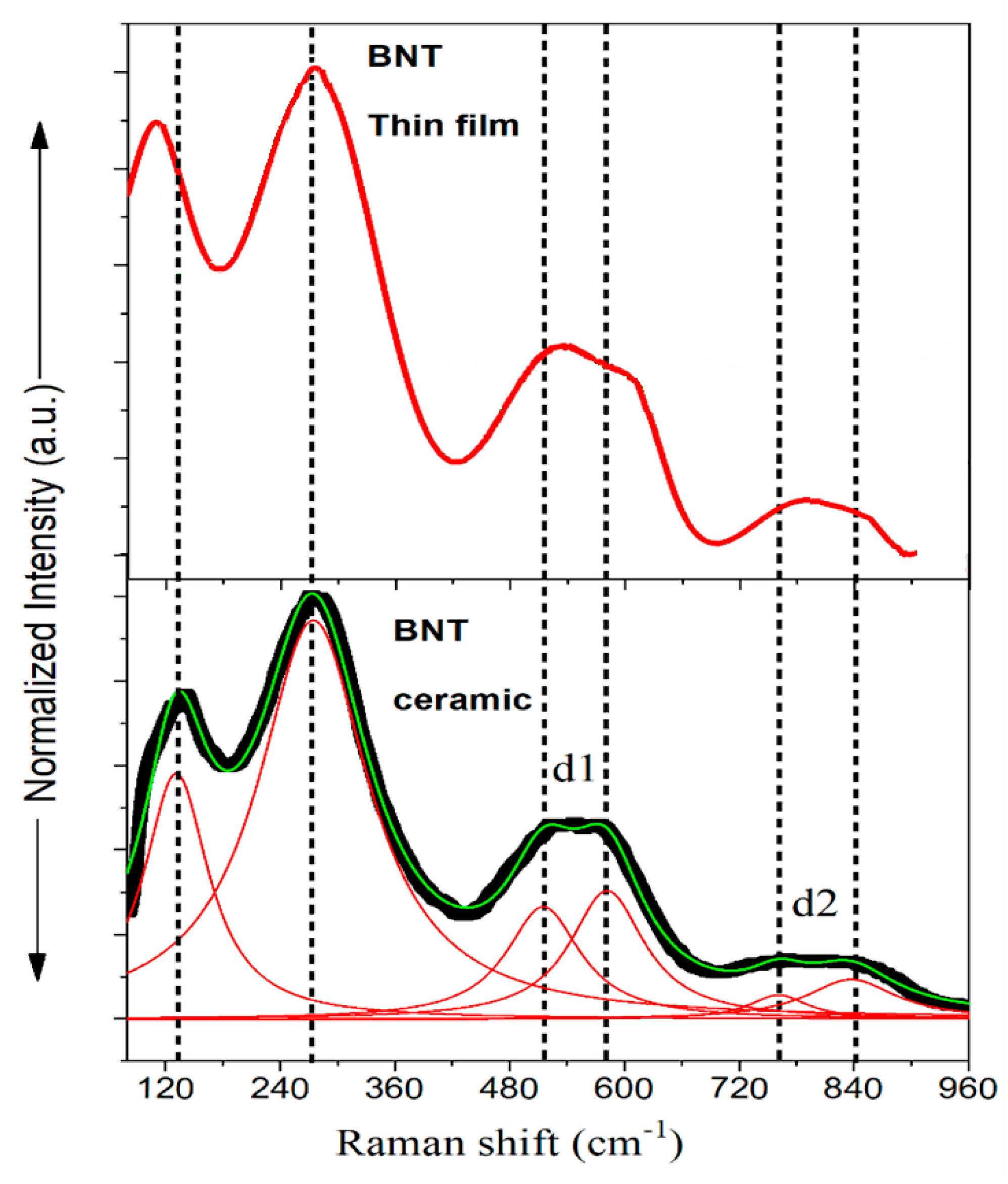
Raman spectroscopy is used in the present work as a powerful tool to get complementary information about the structural changes, which are not accessible by XRD technique. The room temperature spectrum of the investigated film is presented in
Figure 5, together with the Raman spectrum of a BNT ceramic given for comparison.
It is worthy to mention that for BNT bulk material with R3c symmetry, the irreducible representation is given by equation 1 [
23]:
Experimentally, these observed modes are broad and overlap each other, and these features are the signature of disorder in the perovskite lattice caused by the random distribution of Bi and Na cations in the A-sites. In addition, the deconvolution of the spectra gives six peaks. The first one is observed at 135 cm
-1 and is attributed to the Na-O vibration lattice. The intense mode observed at 275 cm
-1 is assigned to the Ti-O vibrations. The four modes observed in the wavenumber interval 400- 900 cm
-1 are related to the vibration and rotation of oxygen octahedra [
24].
The obtained modes are given in the
Table 1, along with a comparison with literature data on ceramics, single crystal, epitaxial and polycrystalline thin films [
7,
12].
The comparison of the Raman spectra presented in the
Figure 5 and the peak data reported in the
Table 1, shows no change in position for the intense band assigned to the Ti-O vibration at 275 cm
-1 almost similar in the bulk ceramic. However, the lower mode corresponding to the Na-O vibration exhibits a downward shift for BNT film. The shift of this mode towards lower frequencies could be attributed for instance, to the increase in the mass of the cations of sublattice A as in the case of the substitution of Na+ with large cation K
+ in the solid solution (Na
1-xK
x)
0.5Bi
0.5TiO
3 [
23]. However in our study, there is no substitution of Na
+ but only a Na-deficiency that might lead to a strong anisotropic lattice distortion, because the
distance is elongated compared to that of Na–O-Na, in agreement with the work of Tyunina et al. [
27]. The authors reported that in ATiO
3 thin films (A= Ba, Sr), the elongation of
compared to Ti-O-Ti induces the stress around the vacancy. With this increase of the chemical bond length while maintaining the same force constant, the vibrational frequency is expected to decrease. Such an effect could explain the low-frequency shift of Na-O vibration mode.
In the BNT ceramic, the high frequency modes (~ 514 cm
-1, ~ 583 cm
-1, ~ 760 cm
-1 and ~ 840 cm
-1) result from TiO
6 octahedral vibrations while cations are almost at rest. These modes are also observed in the thin film. Concerning the modes ~ 514 cm
-1 and ~ 583 cm
-1 (doublet d1), it is reported that the evolution of these bands is governed by the increase of the average ion radii of cations in sublattice A as in the case of the BNT-BT solid solution [
28] or rare earth doped BNT ceramics [
29,
30]. It is worthy to note that in the pure BNT ceramic, these two modes are reported with equal intensity, forming thus a plateau like band [
24]. However, while increasing temperature (or doping) the intensity of the first mode becomes the dominant one whereas the second one vanished as reported in the cited references above. In a study carried out on BNT single crystal, Liang Luo et al. [
31], have correlated this behavior to the presence of the Ti-O rotations with short correlation lengths. Regarding these modes in the present study, the intensity of the first mode is a little bit more intense.
The vibration modes observed around 760 and 840 cm
-1 for BNT ceramic (doublet d2) are well known to involve oxygen atoms vibrations. As depicted from the figure, these two modes seem merged to a broad one in the BNT thin film. The occurrence of oxygen vacancies should affect the bond length and angles of the oxygen octahedra [
32]. An expansion in octahedra could lead to an increase of the bond length between the ions, and thus could reduce the stiffness of the bond leading to the downshift in frequency [
33]. The vibration modes ~ 514 cm
-1 and ~ 583 cm
-1, do not follow the same trend as the ceramic, meaning that not only the strain induced by oxygen vacancies can explain the evolution of these modes [
33].
The displacement of Raman spectra may be caused by stresses/strains in different directions and individual stress tensors for a given data a reported by Atkinson et al. [
34]. Therefore, as is suggested by Wolf et al. [
35] the interpretation of the Raman results needs the knowledge of the stress state in the studied material. Thus, combining Raman spectroscopy with other advanced techniques such as low angle X-ray diffraction, neutron and cyclotron diffraction can give more information about the unknown stress states in the investigated material.
3.3. Dielectric, leakage current, and ferroelectric properties
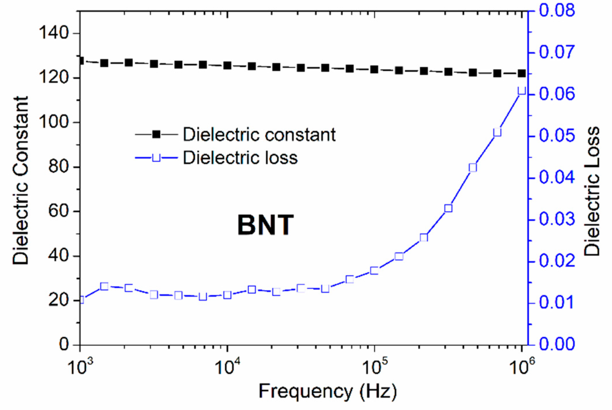
Figure 6 shows the frequency dependence of the dielectric constant and dielectric loss tan δ for BNT thin film annealed under O
2 atmosphere. It is seen that the frequency dispersion of the dielectric constant is quite low, as the dielectric constant remains constant over a large frequency range but its value still very small comparable to what is observed for BNT thin film [
36]. Interestingly, low dielectric loss is obtained, demonstrating the prepared thin film will tend to have a high breakdown voltage limit.
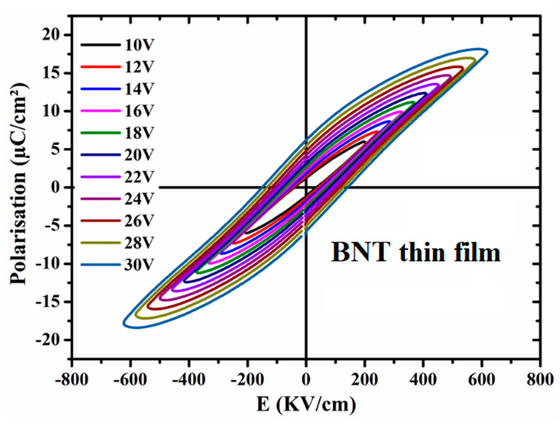
Figure 7 shows the ferroelectric properties at room temperature for the investigated BNT thin film. The film exhibits a typical ferroelectric character with a well-defined hysteresis loops, comparable to the reported literature [
20,
21]. Noting that for BNT ceramic a huge hysteresis loop is reported and was attributed to the contribution of leakage related to the BNT defect chemistry [
29]. For the present films, the obtained almost saturated P-E loop is recorded at a very high applied electric field.
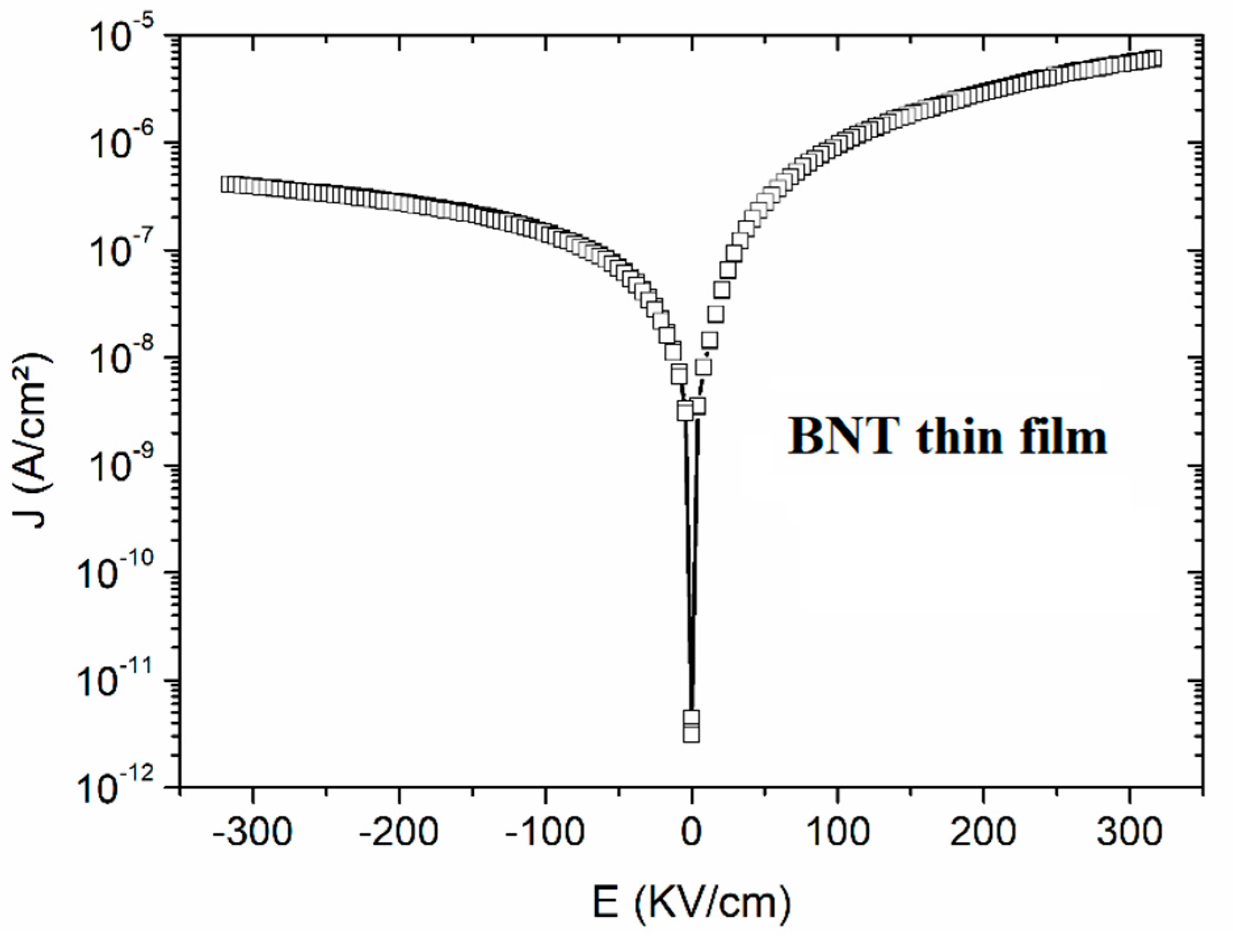
Leakage current property is also investigated for the studied BNT film as illustrated in the
Figure 8. An asymmetric curve is observed because of the asymmetric metal work function of the top Au and bottom Pt electrodes [
37]. It can be seen from the plots that the leakage current density of BNT thin film is lower by several orders of magnitude compared with the ceramic or with some reported thin film data [
19]. It is probably that Na-deficiency (Bi-excess depicted for EXD analysis) leads to the creation of a donor state, which compensates oxygen vacancies and thus, contributes to the improvement of the electrical properties.
It is worth noting that in the present work, BNT solution is prepared without any excess of the starting reagent to compensate the Bi and/or Na deficiency that could result from the volatility of Bi
2O
3 and Na
2O during the synthesis process. The induced Bi/Na-vacancies are expected to be compensated by oxygen vacancies according to the following equations (2 and 3) (Kröger-Vink notation):
Obviously, the presence of oxygen vacancies is expected to induce high dielectric loss of the material. However, the BNT-O
2 film show good dielectric properties with frequency stability of both the dielectric constant and the dielectric losses as well as good ferroelectricity. Recall that in EDX the At% of Bi is very higher compared to the At% of Na, thus we surmise that the mass of Bi
2O
3 is in excess compared to Na
2O. In this case, the excess will compensate not only the volatility of Bi
2O
3 but also that of Na
2O, and by this way, it limits the creation of oxygen vacancies according to the equation 4:
3.4. Energy storage investigation
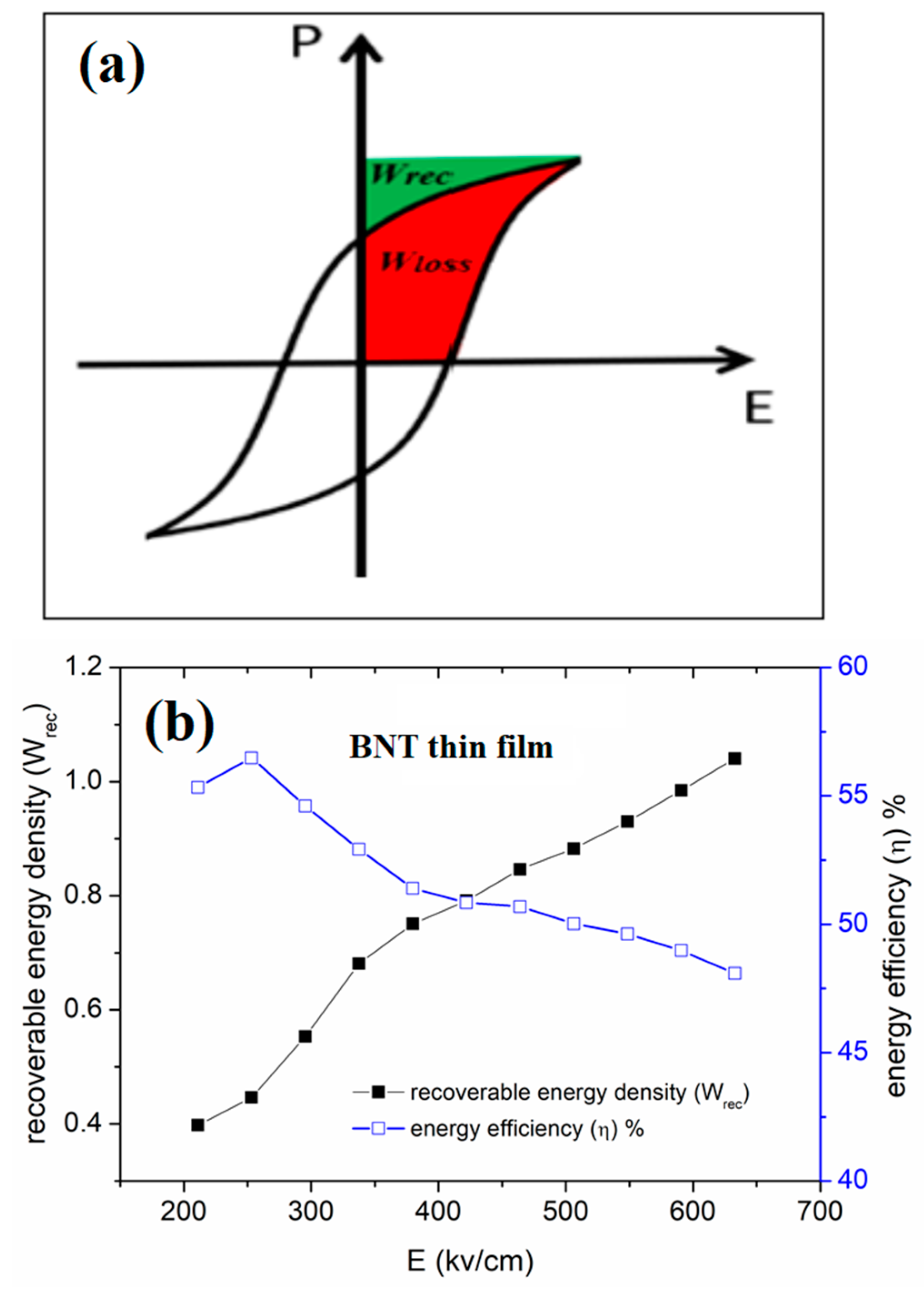
The energy storage density and the efficiency (η) can be determined from the P-E hysteresis loop using the following equations (5 and 6):
where P is the polarization, (W
rec) is the recoverable energy density, E is the applied field, and (W
loss) is the energy loss density as it shown from
Figure 9a, given by equation 7:
The variation of the obtained energy density and efficiency as a function of applied field is presented in
Figure 9b.
The investigated film shows an interesting high recovered energy density that exceeds 1 J/cm3 and an efficiency of 50% under a low electric field E of only 630 kV/cm that demonstrates the better dielectric rigidity with a high breakdown electric field compared with the BNT-based ceramics. Noting that the breakdown field is not achieved in our experience because of the device limitation. Thus, we expect an increase of the recovered energy with the applied electric field.
4. Conclusions
In summary, lead-free polycrystalline, thin film of Bi0.5Na0.5TiO3 was prepared on Pt/SiN substrate by the sol-gel method under O2 atmosphere. Both SEM and AFM images allowed the analysis of the film microstructure. EDX analysis showed that the investigated film is Na- deficient. Pure perovskite phase with R3c rhombohedral symmetry was evidenced by X-ray diffraction using grazing incidence method and it was corroborated with Raman investigation. Furthermore, dielectric, ferroelectric, and leakage current properties were investigated at room temperature and revealed that the BNT thin film showed good electrical properties with a high frequency stability of the dielectric constant, low dielectric losses and good ferroelectric properties with well saturated hysteresis loop, along with low leakage current density. One defect mechanism was suggested where the Na-deficiency leads to the creation of a donor state, which compensates oxygen vacancies and reduce leakage current in the BNT thin film prepared under oxygen atmosphere. The film presents also attractive electrostatic energy storage properties at low applied electric field, which significantly exceeds of the values reported for BNT-based ceramics.
Author Contributions
Conceptualization, A.L. and N.L.; validation, A.L., and N.L.; formal analysis, I.A and M.M.; investigation, A.C., D.F; data curation, I.A., M.M., F.L; writing—original draft preparation, A.L., I.A.; writing—review and editing, N.L,.F.L, A.L; supervision, A.L. and N.L.;. All authors have read and agreed to the published version of the manuscript.
Funding
This work was supported by the Region of Hauts de France (project OPPEN). I. A. acknowledges financial support from the Region of Hauts de France and Amiens Metropole.
Data Availability Statement
Not applicable.
Conflicts of Interest
The authors declare no conflict of interest.
References
- Scott JF, Araujo CAP de (1989) Ferroelectric Memories. Science 246:1400–1405. [CrossRef]
- Jaffe H (1958) Piezoelectric Ceramics. J American Ceramic Society 41:494–498. [CrossRef]
- Katzke H, Dietze M, Lahmar A, et al (2011) Dielectric, ultraviolet/visible, and Raman spectroscopic investigations of the phase transition sequence in 0.71Pb(Mg1/3Nb2/3)O3-0.29PbTiO3 crystals. Phys Rev B 83:174115. [CrossRef]
- Suchanicz J, Ptak WS (1990) On the phase transition in Na0.5Bi0.5TiO3. Ferroelectrics Letters Section 12:71–78. [CrossRef]
- Hiruma Y, Nagata H, Takenaka T (2009) Thermal depoling process and piezoelectric properties of bismuth sodium titanate ceramics. Journal of Applied Physics 105:084112. [CrossRef]
- Bai Y, Zheng G-P, Shi S-Q (2011) Abnormal electrocaloric effect of Na0.5Bi0.5TiO3–BaTiO3 lead-free ferroelectric ceramics above room temperature. Materials Research Bulletin 46:1866–1869. [CrossRef]
- Zannen M, Belhadi J, Benyoussef M, et al (2019) Electrostatic energy storage in antiferroelectric like perovskite. Superlattices and Microstructures 127:43–48. [CrossRef]
- Quignon S, Soyer C, Remiens D (2012) Synthesis and Electrical Properties of Sputtered (Na 0.5 Bi 0.5 )TiO3 Thin Films on Silicon Substrate. J Am Ceram Soc 95:3180–3184. [CrossRef]
- Yu T, Kwok KW, Chan HLW (2007) Preparation and properties of sol–gel-derived Bi0.5Na0.5TiO3 lead-free ferroelectric thin film. Thin Solid Films 515:3563–3566. [CrossRef]
- Peng C, Li J-F, Gong W (2005) Preparation and properties of (Bi1/2Na1/2)TiO3–Ba(Ti,Zr)O3 lead-free piezoelectric ceramics. Materials Letters 59:1576–1580. [CrossRef]
- Chen Z, Hu J (2009) Piezoelectric and dielectric properties of (Bi0.5Na0.5)0.94Ba0.06TiO3–Ba(Zr0.04Ti0.96)O3 lead-free piezoelectric ceramics. Ceramics International 35:111–115. [CrossRef]
- Lin D, Kwok KW (2010) Dielectric and piezoelectric properties of (Bi1−x−yNdxNa1−y)0.5BayTiO3 lead-free ceramics. Current Applied Physics 10:422–427. [CrossRef]
- Shannon RD (1976) Revised effective ionic radii and systematic studies of interatomic distances in halides and chalcogenides. Acta Cryst A 32:751–767. [CrossRef]
- Panda PK (2009) Review: environmental friendly lead-free piezoelectric materials. J Mater Sci 44:5049–5062. [CrossRef]
- Wu J, Xiao D, Zhu J (2012) Effect of (Bi, La)(Fe, Zn)O 3 thickness on the microstructure and multiferroic properties of BiFeO 3 thin films. Journal of Applied Physics 112:094109. [CrossRef]
- Bousquet M, Duclère J-R, Orhan E, et al (2010) Optical properties of an epitaxial Na0.5Bi0.5TiO3 thin film grown by laser ablation: Experimental approach and density functional theory calculations. Journal of Applied Physics 107:104107. [CrossRef]
- Gallegos-Melgar A, Espinosa-Arbelaez DG, Flores-Ruiz FJ, et al (2015) Ferroelectric properties of manganese doped (Bi1/2Na1/2)TiO3 and (Bi1/2Na1/2)TiO3–BaTiO3 epitaxial thin films. Applied Surface Science 359:923–930. [CrossRef]
- Dargham SA, Ponchel F, Abboud N, et al (2018) Synthesis and electrical properties of lead-free piezoelectric Bi0.5Na0.5TiO3 thin films prepared by Sol-Gel method. Journal of the European Ceramic Society 38:1450–1455. [CrossRef]
- Bousquet M, Duclère J-R, Orhan E, et al (2010) Optical properties of an epitaxial Na0.5Bi0.5TiO3 thin film grown by laser ablation: Experimental approach and density functional theory calculations. Journal of Applied Physics 107:104107. [CrossRef]
- Zannen M, Dietze M, Khemakhem H, Es-Souni M (2014) Ferroelectric (Na1/2Bi1/2)TiO3 thin films showing photoluminescence properties. Appl Phys A 117:1485–1490. [CrossRef]
- Maiwa H, Kogure T, Sakamoto W, Hayashi T (2010) Preparation and Properties of Bi 0.5 Na 0.5 TiO 3 Thin Films by Chemical Solution Deposition. Ferroelectrics 405:204–210. [CrossRef]
- Yang CH, Yao Q, Qian J, et al (2018) Growth, microstructure, energy–storage and dielectric performances of chemical–solution NBT–based thin films: Effect of sodium nonstoichimometry. Ceramics International 44:9152–9158. [CrossRef]
- Kreisel J, Glazer AM, Jones G, et al (2000) An x-ray diffraction and Raman spectroscopy investigation of A-site substituted perovskite compounds: the (Na 1- x K x ) 0.5 Bi 0.5 TiO 3 (0le xle 1) solid solution. J Phys: Condens Matter 12:3267–3280. [CrossRef]
- Benyoussef M, Zannen M, Belhadi J, et al (2020) Complex impedance and Raman spectroscopy of Na0.5(Bi1-xDyx)0.5TiO3 ceramics. Ceramics International 46:10979–10991. [CrossRef]
- Luo L, Ge W, Li J, et al (2011) Raman spectroscopic study of Na 1/2 Bi 1/2 TiO 3 -x%BaTiO 3 single crystals as a function of temperature and composition. Journal of Applied Physics 109:113507. [CrossRef]
- Suchanicz J, Jankowska-Sumara I, Kruzina TV (2011) Raman and infrared spectroscopy of Na0.5Bi0.5TiO3 - BaTiO3 ceramics. J Electroceram 27:45–50. [CrossRef]
- Tyunina M, Pacherova O, Kocourek T, Dejneka A (2021) Anisotropic chemical expansion due to oxygen vacancies in perovskite films. Sci Rep 11:15247. [CrossRef]
- Suchanicz J, Jankowska-Sumara I, Kruzina T V. (2011) Raman and infrared spectroscopy of Na0.5Bi0.5TiO 3 - BaTiO3 ceramics. Journal of Electroceramics 27:45–50. [CrossRef]
- Benyoussef M, Zannen M, Belhadi J, et al (2018) Dielectric, ferroelectric, and energy storage properties in dysprosium doped sodium bismuth titanate ceramics. Ceramics International 44:19451–19460. [CrossRef]
- Benyoussef M, Zannen M, Belhadi J, et al (2021) Structural, dielectric, and ferroelectric properties of Na0.5(Bi1-xNdx)0.5TiO3 ceramics for energy storage and electrocaloric applications. Ceramics International 47:26539–26551. [CrossRef]
- Luo L, Ge W, Li J, et al (2011) Raman spectroscopic study of Na 1/2 Bi 1/2 TiO 3 -x%BaTiO 3 single crystals as a function of temperature and composition. Journal of Applied Physics 109:113507. [CrossRef]
- Gouget G, Duttine M, Chung U-C, et al (2019) High Ionic Conductivity in Oxygen-Deficient Ti-Substituted Sodium Niobates and the Key Role of Structural Features. Chem Mater 31:2828–2841. [CrossRef]
- David Tuschel (2019) Stress, Strain, and Raman Spectroscopy. Spectroscopy 34:10–21.
- Atkinson A and Jain S C (1999) Spatially resolved stress analysis using Raman spectroscopy. J. Raman. Spectrosc. 30: 885–891. [CrossRef]
- De Wolf I, Maes HE and Jones SK (1996) Stress measurements in silicon devices through Raman spectroscopy: Bridging the gap between theory and experiment. J. Appl. Phys.79: 7148–7156. [CrossRef]
- C.H. Yang, Z. Wang, Q.X. Li, J.H. Wang, Y.G. Yang, S.L. Gu, D.M. Yang, J.R. Han, ferroelectric films prepared by chemical solution decomposition, Journal of Crystal Growth 284 (1) (2005) 136–141. [CrossRef]
- Ji H, Yu P (2021) Structure, dielectrical properties and capacitance properties of Ba 0.3 Sr 0.7 Zr 0.18 Ti 0.82 O 3 /BaTiO 3 hetero-structure thin films with different BTO layer thicknesses. Mater Res Express 8:026303. [CrossRef]
|
Disclaimer/Publisher’s Note: The statements, opinions and data contained in all publications are solely those of the individual author(s) and contributor(s) and not of MDPI and/or the editor(s). MDPI and/or the editor(s) disclaim responsibility for any injury to people or property resulting from any ideas, methods, instructions or products referred to in the content. |
© 2023 by the authors. Licensee MDPI, Basel, Switzerland. This article is an open access article distributed under the terms and conditions of the Creative Commons Attribution (CC BY) license (http://creativecommons.org/licenses/by/4.0/).
