
Submitted:
29 July 2023
Posted:
01 August 2023
You are already at the latest version
Abstract
In this paper, the performance of Cu-(In,Ga)-S2 (CIGS2) solar cells with adjusting composite CGI-ratio absorber is explored and compared through an improved three-stage co-evaporation technique. For co-evaporating CIGS2 absorber as a less toxic alternative to Cd-containing film, we analyse the effect of the CGI-ratio stoichiometry and crystallinity, and explore its opto-electric sensing characteristic of individual solar cell. The results of this research signify the potential of high-performance CIGS2-absorption solar cells for photovoltaic (PV)-module industrial applications. For the optimal CIGS2-absorption film (CGI=0.95), the Raman main-phase signal (A1) falls at 291 cm-1, which is excited by the 532-nm line of Ar+-laser. Using photo-luminescence (PL) spectroscopy, the corresponding main-peak bandgaps measured is 1.59 eV at the same CGI-ratio film. Meanwhile, the best conversion efficiency (=3.212%) and the average external quantum efficiency (EQE=51.1% in the visible-wavelength region) of photo-electric properties were achieved for the developed CIGS2-solar cells (CGI=0.95). The discoveries of this CIGS2-absorption PV research provide a new scientific understanding of solar cells. Moreover, this research undeniably contributes to a major advancement towards practical PV-module applications and can help more to build an eco-friendly community.
Keywords:
Cu-(In
; Ga)-S2 (CIGS2) solar cells
; Three-stage co-evaporation technique
; CGI-ratio stoichiometry
; Opto-electric sensing performance
; Eco-friendly community
I. Introduction
In the recent years, photovoltaic (PV) technologies have the most abundant form of renewable energy of a fast-growing industry [1]. For many PV technologies, solar cells with thin-film polymers have attracted extensive attention due to their advantages such as light weight, and manufacturing flexibility [2]. Amongst thin-film PV cells with a copper-indium-gallium-selenide (CIGSe) absorber [3,4,5], a low-temperature fabrication process can be applied to a glass or flexible polyimide (PI) substrate for building-integrated industry PV applications [6]. However, when the substrate temperature is below 500 °C, alkali elemental (Na) diffusion from the substrate is limited for the high-efficiency CIGSe solar cells [7]. In order to solve this limitation, three-stage process with Na postdeposition treatment (PDT) is reported [8], thus improving the crystallinity and the grain size of the CIGSe absorption layer deposited for the low-temperature process.
However, the impact on environmental issues and human health has recently been regarded as one of the top priorities. Therefore, developing alternatives to highly toxic cadmium (Cd)-containing materials has become a primary issue in the eco-friendly research. Thus, a copper-indium-gallium-sulfur (CIGS2) can be used as a less toxic alternative to Cd-containing semiconductors. Moreover, CIGS2 is a promising absorber material for the fabrication of high-efficiency thin-film solar cells thanks to its well-adapted bandgap (approximately 1.5 eV) [9,10]. A gradient in the Ga distribution has also been found, CIGS2 was also investigated to be an absorber for the top cell of the tandem configuration [11].
For the CIGS2-solar cell fabrication in this study, the absorber layer was prepared by a modified three-stage sequential co-evaporation method [7], which can effectively adjust the ratio of the CGI process. In this approach combined with an additional Cu-rich for composite-ratio (CGI ratio for Cu-contents of Cu/(In+Ga)) deposition phase and an annealing process was utilized by different process duration after stage 2. Such method has shown tremendous potential to improve the crystallinity of the CIGS2 films deposited at low temperatures.
At the same time, X-ray diffraction (XRD) analysis, Raman-shift spectroscopy, and photo-luminescence (PL) spectroscopy are used to study the crystallization characteristics of the CIGS2 absorber layer with different CGI ratios. Two main objectives of this experiment are to increase conversion efficiency (η) and to improve the external quantum efficiency (EQE) in the visible-wavelength region, all for CGI ratio (composite-ratio polymer) approaches 1 of the developed CIGS2-solar cells. Under the premise of environmental protection for promoting the commercialization of these technologies, we expect to diminish the manufacturing temperature, lessen the toxic material and reduce the production cost. These eco-friendly cells could be effectively applied to mass production for commercial PV-module applications.
II. Experiments and Measurements
For the modified three-stage co-evaporation method in this study, four evaporation sources including Cu, In, Ga, and S were deposited on the substrate as the absorption layer. Table 1 illustrates the deposition parameters of the CIGS2 thin-film absorption layer for preparing sample S1, S2 and S3 with different CGI ratios [12], respectively as 0.78, 0.95 and 1.25. All the parameters were varied by the substrate temperature (°C) and the evaporation time (minutes) of adding the evaporation source (✓check marked) during each stage co-evaporation process.
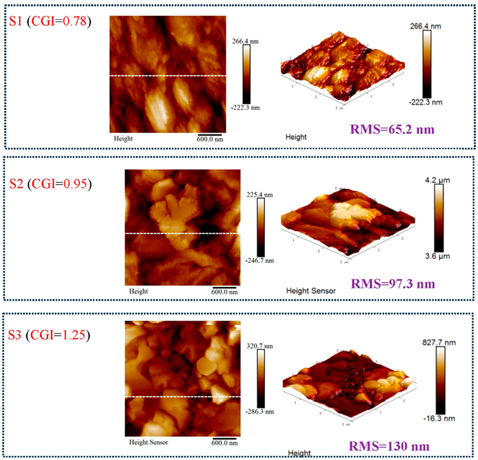
To investigate the characteristics for the three samples with different absorption layers, Table 2 summarizes the surface composition and the corresponding images of energy-dispersive X-ray spectroscopy (EDS) spectrum of their respective absorption layers. The CGI ratios of sample S1, S2 and S3 are separated for 0.78, 0.95 and 1.25. Meanwhile, the sample S2 (GGI=0.10 for Ga/(Ga+In)) of this table conforms that CIGS2 is a high-efficiency device, and the content of Ga atoms (between 0.1 and 0.3) to the GGI in Ga [12]. The crystal structure of films was evaluated by a Rigaku x-ray diffraction (XRD) with Ni-filtered Cu Ka radiation. An atomic force microscope (AFM) instrument (Bruker INNOVA SPM) was used to scan the surface terrain in a typical area of 2.5×2.5 mm2 (512×512 pixels) of the CGIS2 film on a vibrating-free platform. The root-mean-square (RMS) surface-roughness values were obtained using the software that came with the instrument. Furthermore, the optical and electrical properties of our cells were also measured using commercially available systems: scanning electron microscopy (SEM) and EDS (Model: JSM-6500F, JEOL Ltd.), Micro-Raman scattering (UniDRON, CL Technology Co.) incorporated with microwave-induced photo-conductance decay (μ-PCD) system (Model: U-2001), PV conversion efficiency measuring system (Model: Oriel-91192/ AM 1.5 GMM), and the EQE measurements (Model: QE-R, Enlitech).
III. Results And Discussion
Figure 1 demonstrates top-view and cross-section SEM images of CIGS2 absorption layers for different CGI ratios. In all cases, the surface morphology is dominated by the underlying granular structure of the CIGS2 which remains visible beneath the over-layers. It can be seen that the grain size of the Cu-poor (sample S1) absorber (0.9 μm of left-Figure 1(a)) is slightly smaller compared with Cu-rich (sample S3) absorber (1.3 μm of left-Figure 1(c)). Meanwhile, the thickness of Cu-poor absorber (1.875 μm of right-Figure 1(a)) is thicker than that of Cu-rich absorber (1.547 μm of right-Figure 1(c)). Moreover, quantization from the EDS spectra of CIGS2 films illustrates the CGI ratios of 0.78, 0.95 and 1.25 for sample S1, S2 and S3, respectively (shown as Table 2). This leads to a slower reaction as well as growth rate leading to the formation of uniform nanoparticles [13]. Furthermore, the incorporation of the Cu-rich (samples S2 and S3) of CIGS2-absorption layer can distinctly boost grain growth and reduce the fine-grain layer, thus greatly improving the absorber crystallinity and reducing the trap state density [14]. Table 3 plots for 2-D and 3-D AFM images of as deposited different CGI-ratio samples. As is evident from S2 image relatively compact and flat surface structure, the film is composed of cone-shaped columns randomly distributed over the surface of the film. Thus, the films’ surface is rough and porous with RMS surface roughness of 97.3 nm. These results are consistent with the results in the literature [14] indicating that a more porous CGI-ratio film structure leads to a greater grain size from Figure 1.
Figure 2 shows XRD patterns (under 5° incident angle) of CIGS2 layers with different CGI ratios. In which, the chalcopyrite structure of these films was determined by XRD using Cu-K radiation of 1.5418 Å. The peak pattern is in good agreement with the Joint Committee on Powder Diffraction Standards (JCPDS) reference diagrams for the corresponding bulk phases. The (112), (204/220) and (116/312) lattice plane, respectively located at 27.9°, 46.5° and 55.0° (2-theta values) from CuInS2 (JCPDS # 00-042-1475). The secondary-phase signal is located at CuS (103) at 32.38°, Mo (110) at 40.5°, MoS2 (104) at 44°, and CuInS2 (440) at 48.06°.
Figure 3 illustrates the Raman spectra of CIGS2 thin-film absorption layers, which exhibits peaks that can be attributed to the phonon modes of the ternary CuInS2 chalcopyrite. The absorption layers were excited by the 532-nm line of an argon (Ar+) laser at room temperature. Meanwhile, the modes of secondary phase are formed during the deposition process. The most peak at 291 cm-1 is assigned to the A1-mode of CuInS2, thus coinciding a noticeable contribution from Cu–Au mode (310 cm-1) in CIGS2 films [15].
At same modulation source as Raman spectra on CIGS2 thin films, Figure 4 plots the energy bandgap (eV) - the photoluminescence (PL) spectra measured at the 600-980-nm wavelength transmission. In which, the Cu-rich with samples S2 and S3, the main peak displaces to about 1.59 and 1.61 eV, possibly induced by the secondary phase of CuS (103) at 32.38o (shown in XRD pattern of Figure 2) [16]. In the lowest CGI-ratio film (sample S1), it doesn’t have an obvious peak. For the sample S2 and S3, they show the obvious and wanted peak at 1.59 and 1.61 eV, respectively. However, sample S1 has the unwanted peak at 1.41 eV of CuIn5S8, thus increasing defect density of the CIGS2 film in concurrence with literature reports [16].
The current density-voltage (J-V) characteristics of solar cells were measured under illumination and under the conditions of AM1.5G and 1000 W/cm2. Figure 5 shows the J-V curve under illumination and the electrical properties of the CGIS2-layer solar cells are summarized on the top. The best performance of the sample S2 (CGI=0.95) yielded the highest efficiency of the CGIS2-layer solar cell, with short-circuit current (JSC) = 15.53 mA/cm2, open-circuit voltage (VOC) =590 mV, series resistance (RS) = 189 Ω, and conversion efficiency (η) = 3.212%, yielding a gain of 2.304%absolute compared to the S1 cell. Although there is improvement in fill factor (F.F.) for the higher CGI-ratio solar cell, it results in larger-JSC value. Upon further investigation, it appears that the cause for the lower CGI-ratio device required with this synthesis technique (CGI ratio~1.0), an approximate 1.6-eV-bandgap phenomena also observed with CuGaS2 absorption layer at the PL-spectra of Figure 4 as described previously, thus improving optoelectronic quality and increasing the charge-carrier lifetime of the absorption layer [17].
Figure 6 shows the EQE effect for our CIGS2-absorption solar cells with different CGI ratios. In this study, for the visible-wavelength range (400–700 nm), the average EQE value of our CIGS2-solar cell was increased as the CGI-ratio was increased, due to the low transmittance of the absorption layer [18]. This was attributed to the light absorption effect [4]—the absorber structure (CIGS2 layer) adopts narrower bandgap of CIGS2 (~1.61 eV), thus avoiding more incident light into the main absorption layer. This phenomenon also indicates that as shown in Figure 5, only a very small number of carriers are generated in the lower CGI-ratio absorption layer after illumination, resulting in a decrease in JSC and η values. Additionally, it can be noticed that in the visible-wavelength range of Figure 6, sample S3 exhibits a great improvement in EQE as compared with sample S1 by approximately 29.8%absolute. This is presumed to be due to the inability of the absorber layer to efficiently extract current in the visible-wavelength region.
For commercial applications of mass production of PV modules, the overall performance will vary significantly under different photo-intensity conditions, which will have a serious impact on the yield of PV systems. Variations in the intensity of solar radiation falling on a PV module affect many of its parameters, including VOC, F.F., conversion efficiency and output power. For a PV module (CGI=0.95) prepared with the optimal CIGS2-solar cells under photo intensity set at 1 KW/m2, Figure 7 plots the current (A)-voltage (mV) cures of a module with varying ambient temperatures. Among them, the VOC value decreases (from 570 to 410 mV) with the increase of the ambient temperature (from 30 to 75 °C). This is the negative-temperature effect of VOC value, which in turn leads to a drop in its η value (from 5.47% to 3.21%) with same point of view on [19].
As photo intensity increases, again the incident photo energy is absorbed more because a greater percentage of the incident light has enough energy to raise charge carriers from the valence band to the conduction band [20]. For a PV module (CGI=0.95), Figure 8 illustrates the output power (W) relation with voltage (V), and it shows a linear upward trend with the gradual increase of photo intensity (from 250 to 1000 W/m2). On the contrary, this is the positive-photo-intensity effect of VOC value, which in turn leads to a raise in its η value (from 1.58% to 5.73%) with the consistency on [20].
IV. Conclusions
In summary, the modified three-stage co-evaporation method was used to prepare the CIGS2-absorber solar cell with adjusting the CGI-ratio to obtain the optimal PV characteristics. All the CIGS2-absorption layers were characterized by the EDS, XRD, Raman and PL spectra, which are persuasive and distinguish the effect of CGI ratios on CIGS2 thin-film layers. For the developed CIGS2-absorption film (CGI=0.95), the Raman main-phase signal (A1) falls at 291 cm-1, which is excited by the 532-nm line of Ar+-laser. Using PL spectroscopy, the corresponding main-peak bandgaps measured is 1.59 eV at the same CGI-ratio film. Meanwhile, the best conversion efficiency (η=3.212%) and the average EQE (=51.1% in the visible-wavelength region) of photo-electric properties were achieved for the developed CIGS2-solar cells (CGI=0.95).
For PV modules used in commercial mass production, the overall performance will vary greatly under different photo intensities. Variations in the intensity of solar radiation falling on a PV module affect many of its parameters, including VOC, F.F., η and output power. For a PV module (CGI=0.95) prepared with the optimal CIGS2-solar cell, the η values decrease with rising ambient temperature. At the same time, its output powers also increase with increasing photo intensity. On the premise of improving the performance of the developed devis, we hope that the proposed technology can not only reduce the process temperature and production cost, but also lessen the toxic Cd-containing materials. Therefore, the eco-friendly PV modules can be effectively applied to commercial mass production.
Acknowledgments
The authors acknowledge financial support from The National Science and Technology Council of R.O.C. under contract No. MOST 108-2221-E-019-054.
References
- International Energy Agency, “Renewables 2019, Market Analysis and Forecast from 2019 to 2024,” IEA Reports, 2019. Available online: https://www.iea.org/reports/renewables-2019 (accessed on 10 February 2023).
- T. I. Alanazi and M. E. Sabbagh, Proposal and Design of Flexible All-Polymer/CIGS Tandem Solar Cell,” Polymers, 15(8), 1823, pp.01-17, 2023. [CrossRef]
- Y. Bourlier, O. Cristini Robbe, C. Lethien, P. Roussel, A. Pastre, M. Zegaoui, R. Bernard, "Control of gallium incorporation in sol–gel derived CuIn(1−x)GaxS2 thin films for photovoltaic applications," Materials Research Bulletin, 70, pp. 137-144, 2015. [CrossRef]
- J.-S. Ho, S.-C. Chang, J.-J. Ho, W.-T. Hsu, C.-C. Chiang, S.-Y. Tsai, S.-S. Wang, C.-K. Lin, C.-C. Chou, C.-H. Yeh and K. L. Wang, “Improving the Performance of Solar Cells with Novel Buffer Structure by the Chemical Bath Deposition Technique,” Materials Science in Semiconductor Processing, 59, pp.29-34 (March 01, 2017). [CrossRef]
- F. Ahmad, T. H. Anderson, P. B. Monk, and A. Lakhtakia, “Efficiency enhancement of ultrathin CIGS solar cells by optimal bandgap grading,” Applied Optics, 58(22), pp.6067-6078, Aug. 2019. [CrossRef]
- M. Nakamura, K. Yamaguchi, Y. Kimoto, Y. Yasaki, T. Kato and H. Sugimoto, "Cd-Free Cu(In,Ga)(Se,S)2 Thin-Film Solar Cell With Record Efficiency of 23.35%," IEEE Journal of Photovoltaics, 9(6), pp. 1863-1867, 2019. [CrossRef]
- P. Santos, D. Brito, P. Anacleto, J. Fonseca, D. de B. Sousa, C. J. Tavares, J. Virtuoso, M. Alves, A. Pérez-Rodríguez, and S. Sadewasser, “Effect of Cu-In-Ga Target Composition on Hybrid-Sputtered Cu(In,Ga)Se2 Solar Cells,” IEEE J. of Photovoltaics, 11(5), pp.1206-1212, Sept. 2021. [CrossRef]
- D. Rudmann, D. Brémaud, A. F. da Cunha, G. Bilger, A. Strohm, M. Kaelin, H. Zogg, and A. N. Tiwari, “Sodium incorporation strategies for CIGS growth at different temperatures,” Thin Solid Films, 480−481, pp.55−60, 2005. [CrossRef]
- W. Li, L. Yao, K. Li, X. Li, B. Yang, S. Xu, S. Shi, C. Yi, M. Chen, Y. Feng, W. Li, Z. Lu, and C. Yang, “Enabling Low-Temperature Deposition of High-Efficiency CIGS Solar Cells with a Modified Three-Stage Co-Evaporation Process,” ACS Applied Energy Materials, 3, pp.4201-4207, 2020. [CrossRef]
- J. Álvarez-Garcı́a, A. Pérez-Rodrı́guez, A. Romano-Rodrı́guez, L. Calvo-Barrio, B. Barcones, J. R. Morante, K. Siemer, I. Luck and R. Klenk, "Microstructural characterisation of CuInS2 polycrystalline films sulfurised by rapid thermal processing," Thin Solid Films, 387(1), pp. 219-221, 2001. [CrossRef]
- S. Merdes, R. Mainz, J. Klaer, A. Meeder, H. Rodriguez-Alvarez, H.W. Schock, and R. Klenk, "12.6% efficient CdS/Cu (In, Ga) S2-based solar cell with an open circuit voltage of 879mV prepared by a rapid thermal process," Solar Energy Materials and Solar Cells, 95(3), pp. 864-869, 2011. [CrossRef]
- G. Hanna, A. Jasenek, U. Rau and H.W. Schock, "Influence of the Ga-content on the bulk defect densities of Cu(In,Ga)Se2," Thin Solid Films. 387, pp. 71-73, 2001. [CrossRef]
- S. Singh, S. K. Samji & M. S. R. Rao. "Synthesis and characterisation of CuInGaS2 nano-ink for photovoltaic applications," J. of Experimental Nanoscience, 8(3), pp. 320-325, 2013. [CrossRef]
- Q. Gao, S. Yuan, Z. Zhou, D. Kou, W. Zhou, Y. Meng, Y. Qi, L. Han, and S. Wu, “Over 16% Efficient Solution-Processed Cu(In,Ga)Se2 Solar Cells via Incorporation of Copper-Rich Precursor Film,” Small, Advanced Science News, 18, 2203443, pp.1-11, 2022. [CrossRef]
- K. Wu and D. Wang, “Temperature-dependent Raman investigation of CuInS2 with mixed phases of chalcopyrite and CuAu,” Phys. Status Solidi A, 208(12), pp.2730–2736.
- S. Nasser, M. N. Alsloum and N. Hussain, “Preparing of Copper Oxides Thin Films by Chemical Bath Deposition (CBD) for Using in Environmental Application,” Energy Procedia, 74, pp.1459-1465, 2015. [CrossRef]
- S. Shukla, M. Sood, D. Adeleye, S. Peedle, G. Kusch, D. Dahliah, M. Melchiorre, G.-M. Rignanese, G Hautier, R. Oliver and S. Siebentritt, “Over 15% efficient wide-band-gap Cu(In,Ga)S2 solar cell: Suppressing bulk and interface recombination through composition engineering,” Joule, 5, pp.1816-1831, July 2021. [CrossRef]
- J. Ho, T.-C. Wu, J.-J. Ho, C.-H. Hung, S.-Y. Chen, J.-S. Ho, S.-Y. Tsai, C.-C. Chou and C.-H. Yeh, “Rear-Surface Line-Contact Optimization Using Screen-Print Techniques on Crystalline Solar Cells for Industrial Applications,” Materials Science in Semiconductor Processing, 83, pp.22-26 (15 Aug, 2018). [CrossRef]
- B. V. Chikate and Y.A. Sadawarte, “The Factors Affecting the Performance of Solar Cell,” International Journal of Computer Applications, 0975-8887, pp.1-5, 2015.
- Z. Li, J. Z. Li, J. Yang and P. A. N. Dezfuli, “Study on the Influence of Light Intensity on the Performance of Solar Cell,” International Journal of Photoenergy, ID 6648739, pp.1-10, 2021. [CrossRef]
Figure 1.
The top view (left) and cross-sectional view (right) of SEM images with the CIGS2 absorber layer for the CGI ratios are: (a) CGI=0.78 (Cu-poor), (b) CGI=0.95, and (c) CGI=1.25 (Cu-rich), respectively. In which, the grain size (from 0.9 to 1.3 μm) increases with copper content for crystal thickness about 1.547~1.875-μm range.
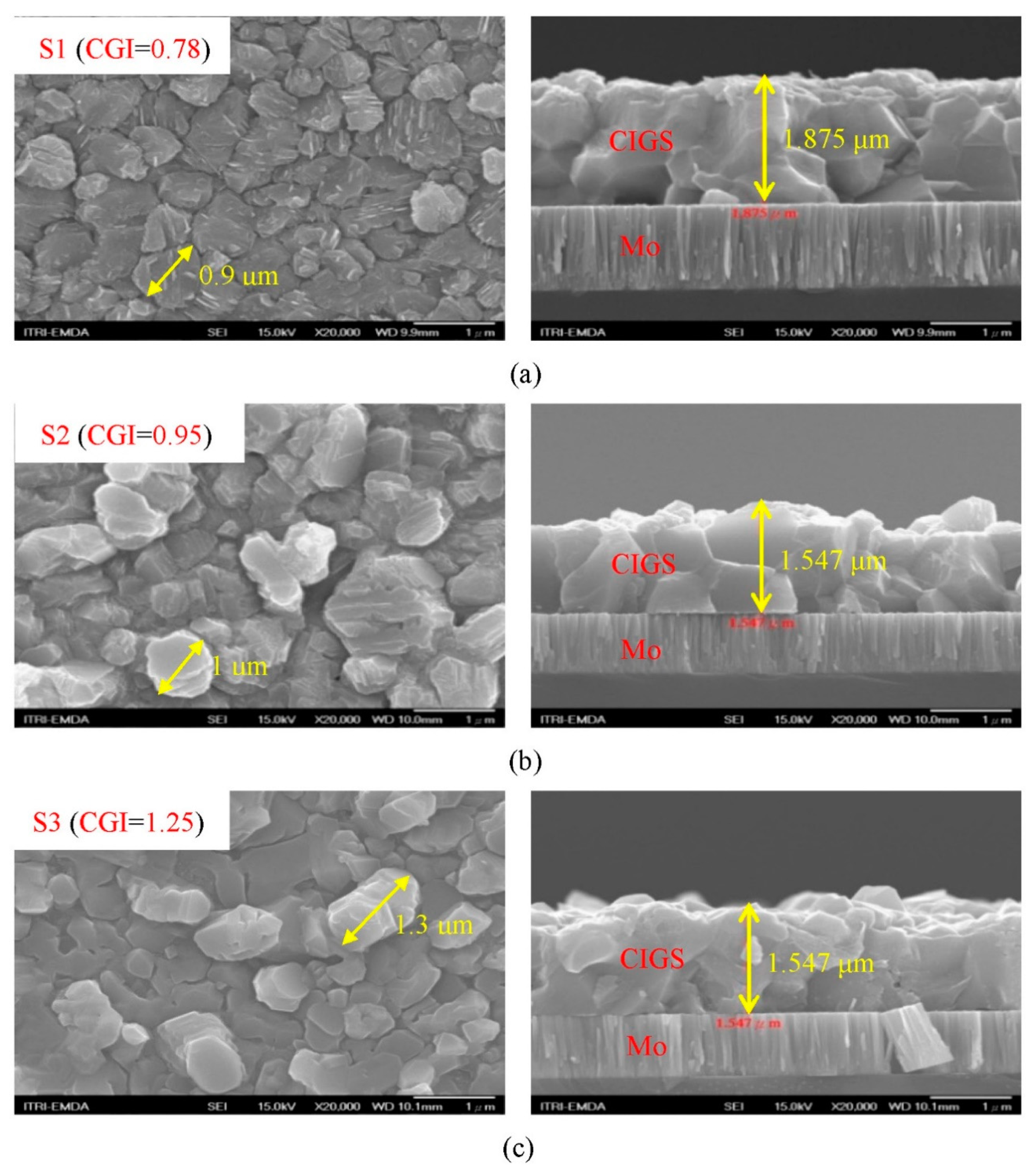
Figure 2.
The X-ray diffractograms (under the 5°incident angle) are mainly in the deeper part of the CIGS2 absorption layer with different CGI ratios. The 2θ values of the main diffraction peaks appear at 27.9°, 46.5° and 55° from zoom-in patterns (inserted images), respectively on (112), (204/220) and (116/312) facets. The secondary-phase signal is located at CuS (103) at 32.38°, Mo (110) at 40.5°, MoS2 (104) at 44°, and CuInS2 (440) at 48.06°.
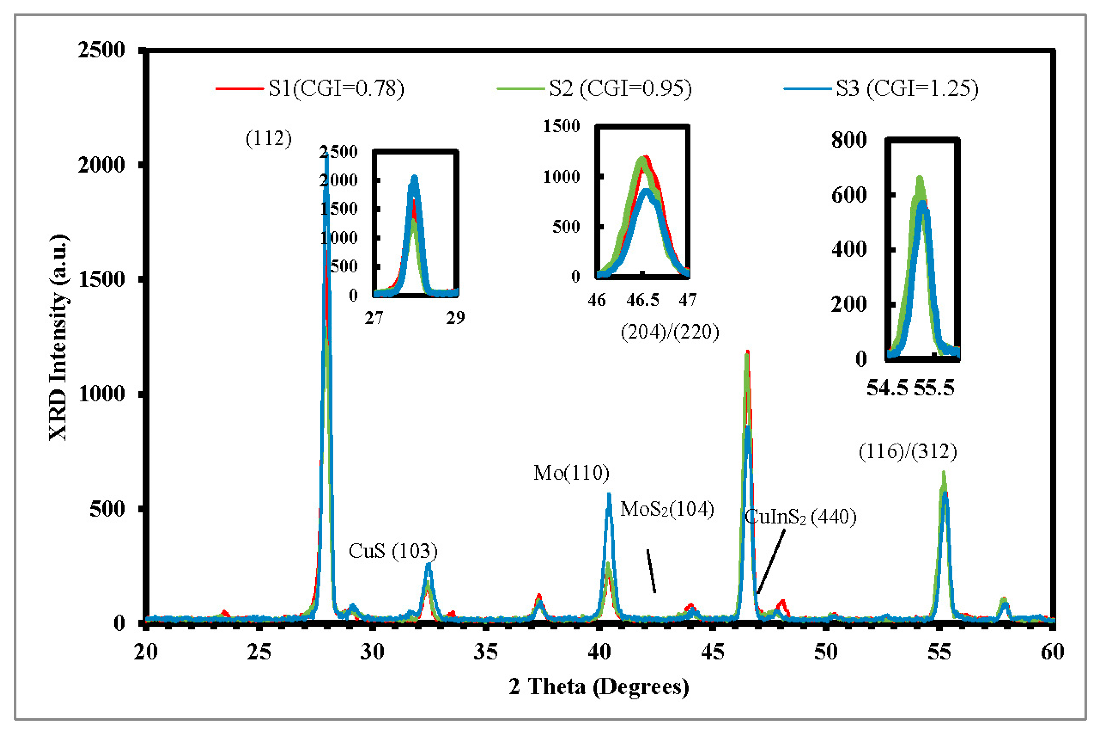
Figure 3.
The Raman spectra of CIGS2 thin film absorption layer prepared with different sample of S1, S2 and S3, which contain various concentrations of Cu-Au ordering. In which, the Raman main-phase signal (A1) falls at 291 cm-1.
Figure 3.
The Raman spectra of CIGS2 thin film absorption layer prepared with different sample of S1, S2 and S3, which contain various concentrations of Cu-Au ordering. In which, the Raman main-phase signal (A1) falls at 291 cm-1.
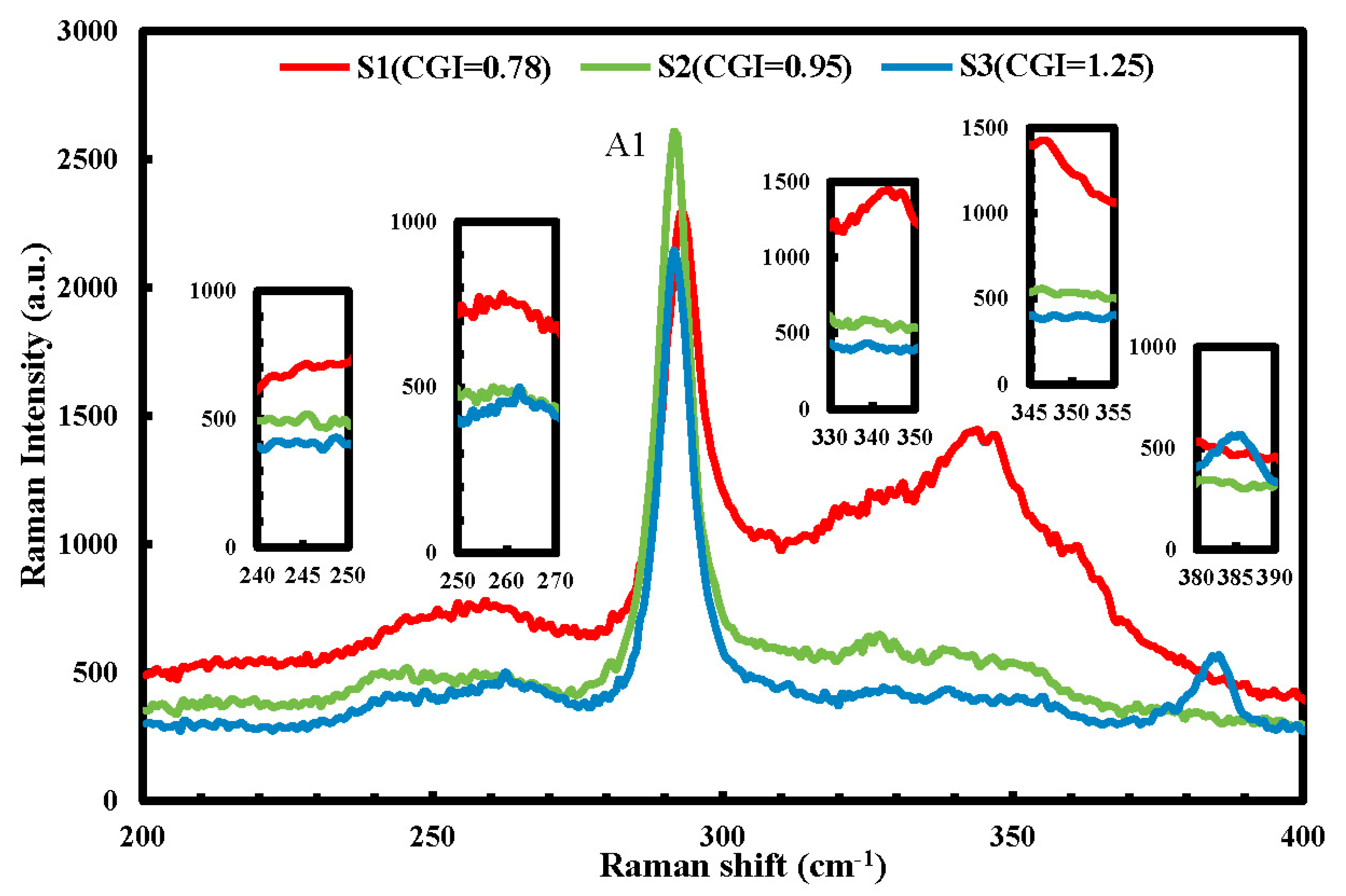
Figure 4.
The photoluminescence (PL) spectra of CIGS2 thin-film absorption layer, which the main-peak bandgaps measured are 1.58,1.59, and 1.61 eV, respectively for S1, S2 and S3 samples.
Figure 4.
The photoluminescence (PL) spectra of CIGS2 thin-film absorption layer, which the main-peak bandgaps measured are 1.58,1.59, and 1.61 eV, respectively for S1, S2 and S3 samples.
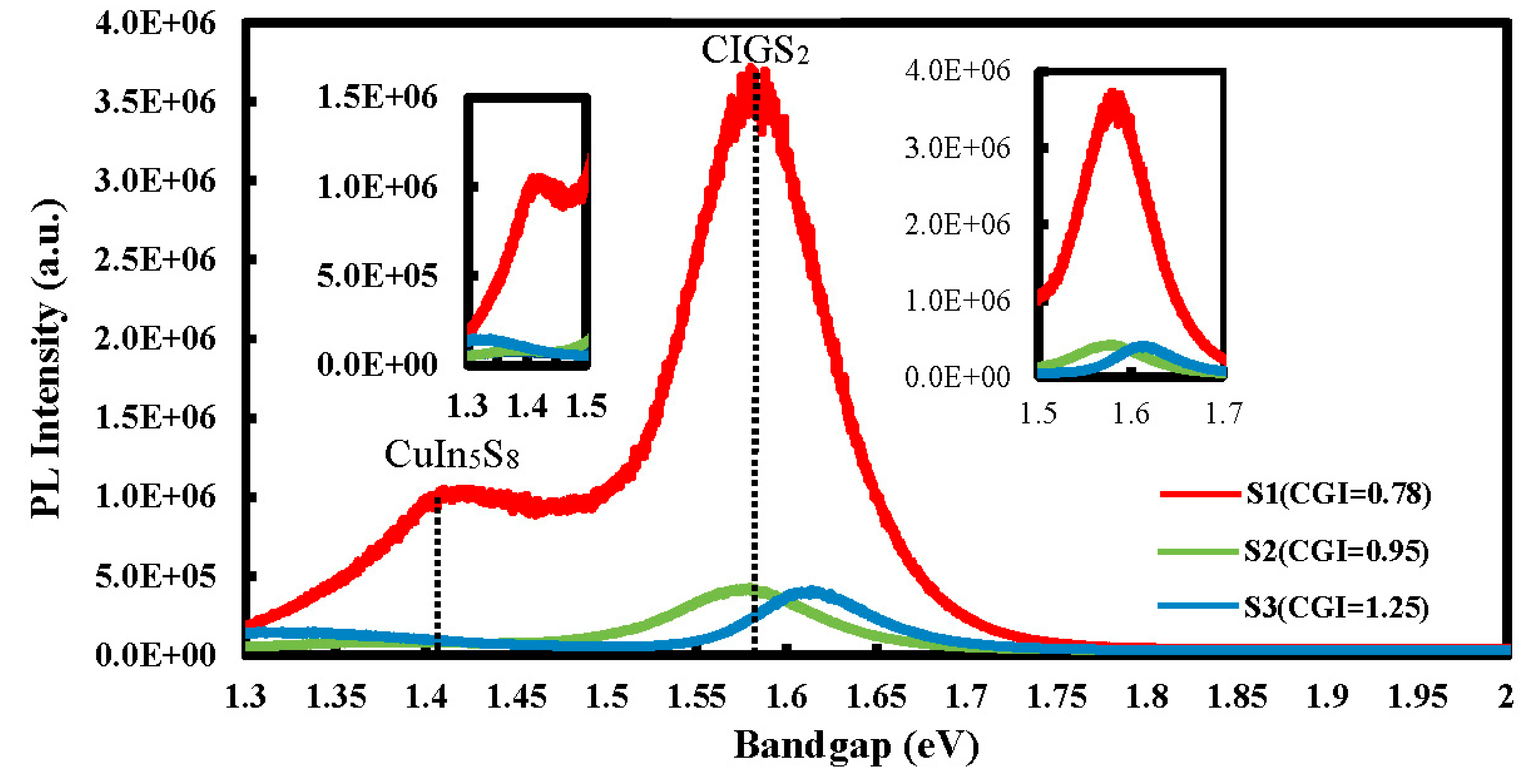
Figure 5.
The current density-output voltage (J-V) curves prepared from different samples of S1, S2 and S3, where the optoelectrical performance of CIGS2-solar cells has been attached on the top.
Figure 5.
The current density-output voltage (J-V) curves prepared from different samples of S1, S2 and S3, where the optoelectrical performance of CIGS2-solar cells has been attached on the top.
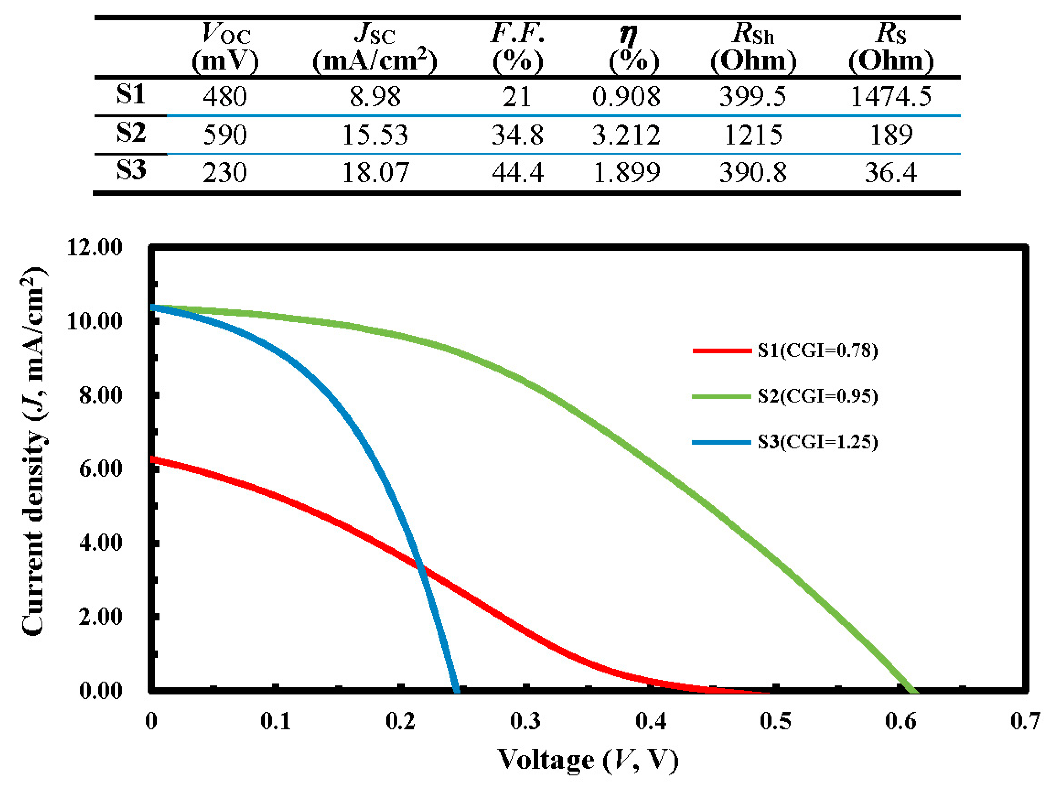
Figure 6.
The EQE of CIGS2-solar cells prepared with different samples of S1, S2 and S3. The sample S3 EQE value (average for the wavelength range of 400-700 nm) is about 51.5% higher than that of the other samples.
Figure 6.
The EQE of CIGS2-solar cells prepared with different samples of S1, S2 and S3. The sample S3 EQE value (average for the wavelength range of 400-700 nm) is about 51.5% higher than that of the other samples.
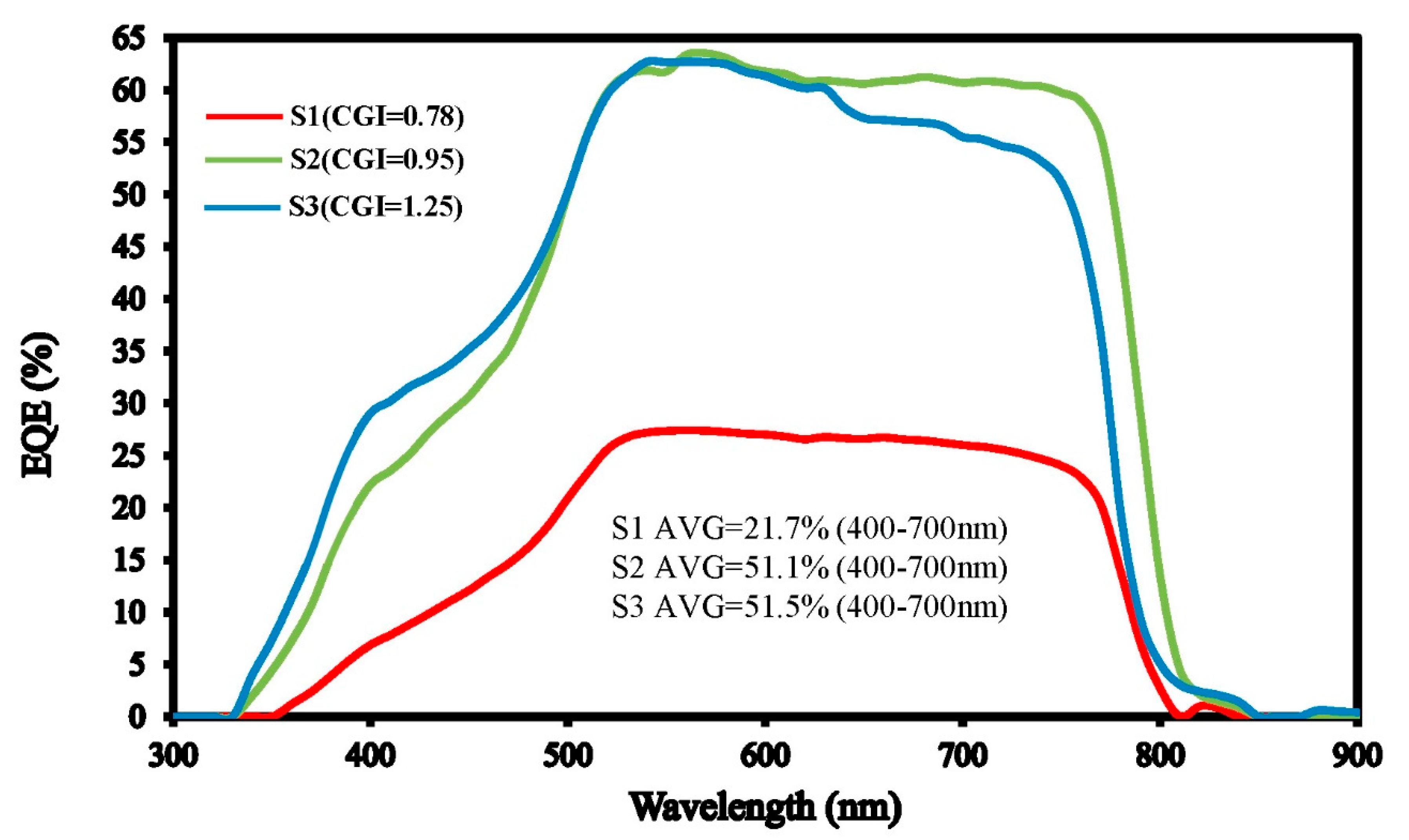
Figure 7.
Under the fixed photo intensity (KW/m2) for the optimal CIGS2-solar cells prepared with a PV module (CGI=0.95), the current-voltage (I-V) curves observed from different ambient temperatures (30~75 °C).
Figure 7.
Under the fixed photo intensity (KW/m2) for the optimal CIGS2-solar cells prepared with a PV module (CGI=0.95), the current-voltage (I-V) curves observed from different ambient temperatures (30~75 °C).
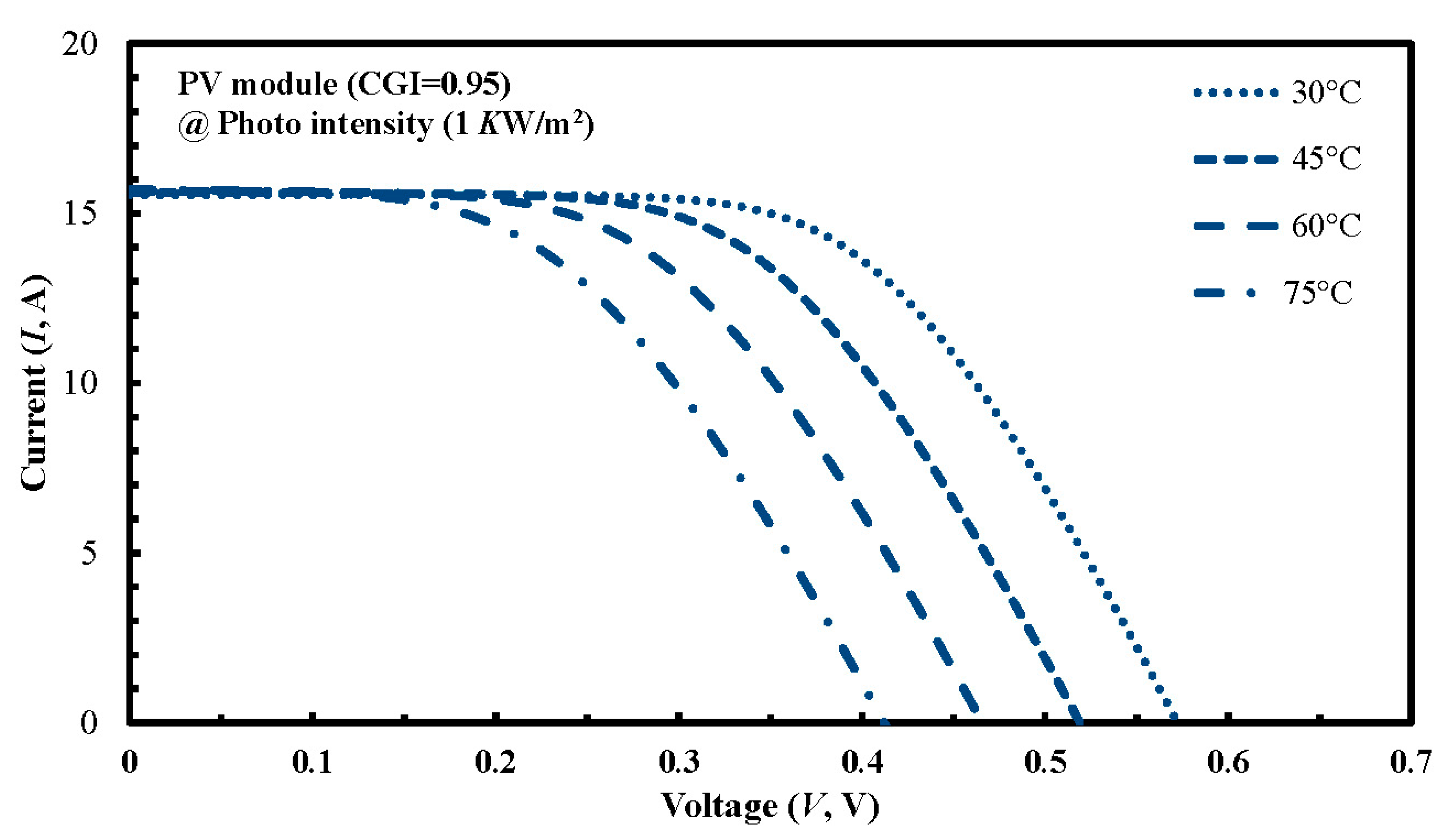
Figure 8.
Under the fixed ambient temperature (25 °C) for a PV module (CGI=0.95) prepared with the optimal CIGS2-solar cells, the output power-voltage (Pout-V) curves observed from variable photo intensity (250~1000 W/m2).
Figure 8.
Under the fixed ambient temperature (25 °C) for a PV module (CGI=0.95) prepared with the optimal CIGS2-solar cells, the output power-voltage (Pout-V) curves observed from variable photo intensity (250~1000 W/m2).
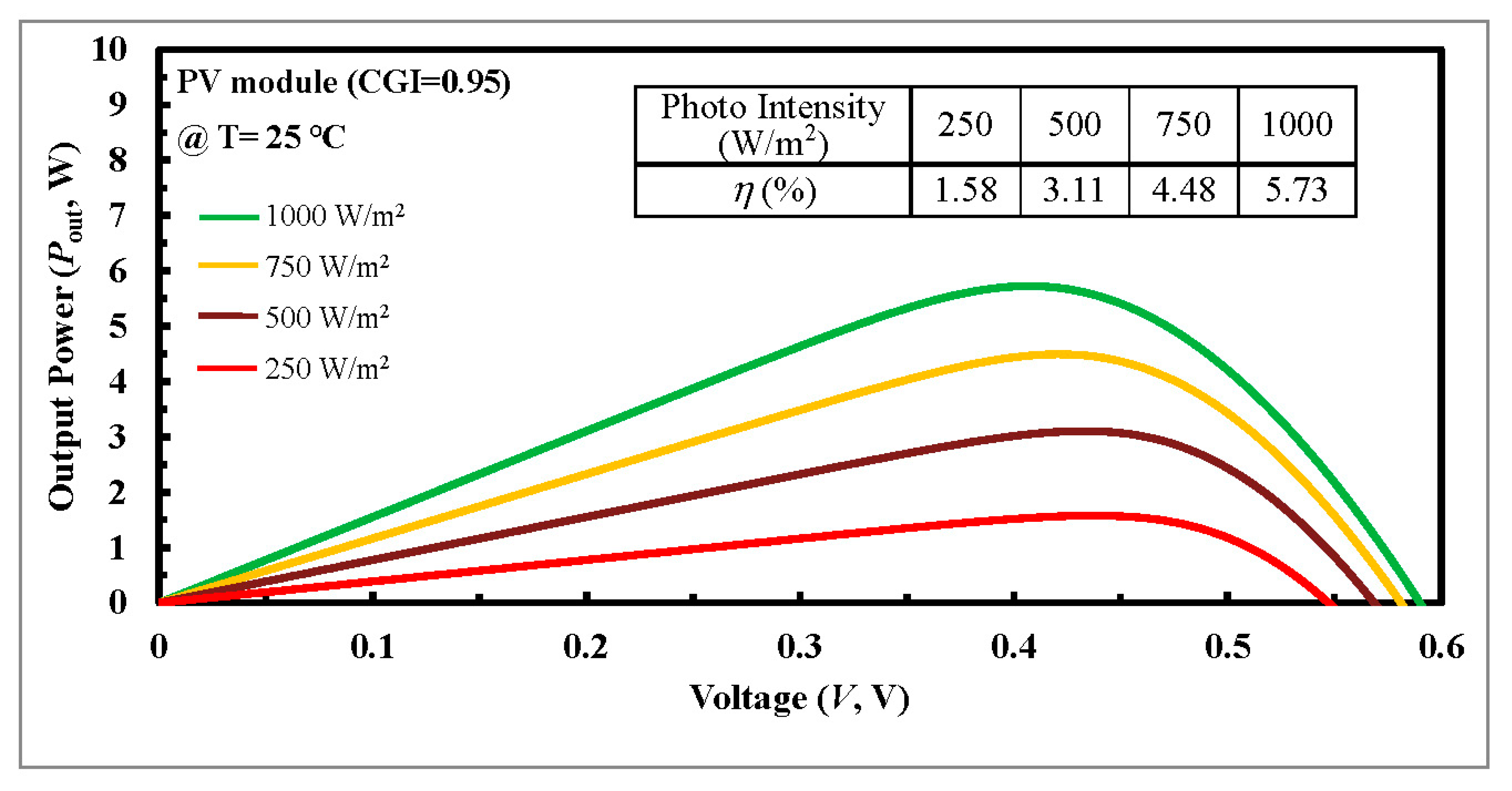

Table 1.
thin-film absorption layer prepared with different CGI ratios, (a) S1 (CGI=0.78), (b) S2 (0.95) and (c) S3 (CGI=1.25).
Table 1.
thin-film absorption layer prepared with different CGI ratios, (a) S1 (CGI=0.78), (b) S2 (0.95) and (c) S3 (CGI=1.25).
| (a) S1 (CGI=0.78) | Cu | In | Ga | S | Temp (oC) | Time (mins) |
| Stage 1 | ✓ | ✓ | ✓ | ✓ | 380 | 48.5 |
| Stage 2 | ✓ | 380-640 | 40 | |||
| Stage 3 | ✓ | ✓ | ✓ | 640 | 20 | |
| (b) S2 (CGI=0.95) | Cu | In | Ga | S | Temp (oC) | Time (mins) |
| Stage 1 | ✓ | ✓ | ✓ | ✓ | 380 | 41 |
| Stage 2 | ✓ | ✓ | 380-640 | 31 | ||
| Stage 3 | ✓ | ✓ | ✓ | 640 | 16 | |
| (c) S3 (CGI=1.25) | Cu | In | Ga | S | Temp (oC) | Time (mins) |
| Stage 1 | ✓ | ✓ | ✓ | ✓ | 380 | 37 |
| Stage 2 | ✓ | ✓ | 380-640 | 33 | ||
| Stage 3 | ✓ | ✓ | ✓ | 640 | 9 |
Table 2.
thin-film absorption layer prepared with different CGI ratios, S1, S2 and S3 for CGI=0.78, CGI=0.95 and CGI=1.25, respectively.
Table 2.
thin-film absorption layer prepared with different CGI ratios, S1, S2 and S3 for CGI=0.78, CGI=0.95 and CGI=1.25, respectively.
| Atomic Ratio (%) | Cu K | In L | Ga K | S K | Mo L | CGI | GGI |
|---|---|---|---|---|---|---|---|
| S1 | 21.12 | 24.63 | 2.43 | 49.03 | 2.79 | 0.78 | 0.08 |
| S2 | 24.33 | 23.05 | 2.43 | 46.6 | 3.59 | 0.95 | 0.10 |
| S3 | 27.21 | 20.68 | 0.98 | 48.75 | 2.38 | 1.25 | 0.04 |
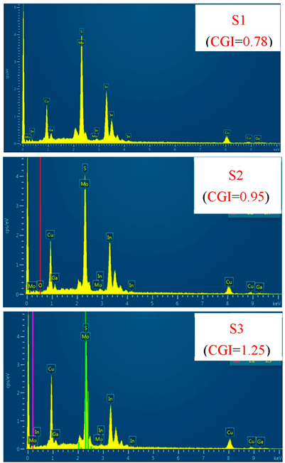 | |||||||
Table 3.
thin-film absorption layer prepared with RMS (Rq) values, S1, S2 and S3 for 65.2, 97.3 and 130 nm, respectively.
Table 3.
thin-film absorption layer prepared with RMS (Rq) values, S1, S2 and S3 for 65.2, 97.3 and 130 nm, respectively.
| RMS (Rq) | Ra | Rmax | |
|---|---|---|---|
| S1 (CGI = 0.78) | 65.2 nm | 50.4 nm | 407 nm |
| S2 (CGI = 0.95) | 97.3 nm | 73.4 nm | 483 nm |
| S3 (CGI = 1.25) | 130 nm | 104 nm | 785 nm |
 | |||
Disclaimer/Publisher’s Note: The statements, opinions and data contained in all publications are solely those of the individual author(s) and contributor(s) and not of MDPI and/or the editor(s). MDPI and/or the editor(s) disclaim responsibility for any injury to people or property resulting from any ideas, methods, instructions or products referred to in the content. |
© 2023 by the authors. Licensee MDPI, Basel, Switzerland. This article is an open access article distributed under the terms and conditions of the Creative Commons Attribution (CC BY) license (http://creativecommons.org/licenses/by/4.0/).
Copyright: This open access article is published under a Creative Commons CC BY 4.0 license, which permit the free download, distribution, and reuse, provided that the author and preprint are cited in any reuse.


