
Submitted:
06 June 2023
Posted:
07 June 2023
You are already at the latest version
Abstract
The object of research is an optical-electronic system for recording and processing signals from fiber-optic sensors. Due to the use of optical fibers as sensitive elements, there is no influence on the measurement result of electromagnetic fields, spurious electromagnetic radiation, channel crosstalk, there are no problems, electrical safety is significantly increased, there are no problems of arcing and sparking. A scheme of a receiving-transmitting module has been developed, which is additionally equipped with a preliminary protection and filtering system. Further, measuring tracks, microcontroller software and functional tests were ordered to determine the metrological properties of the proposed system.Signal integrity analysis is presented, which allows you to check whether the signals present in the device are correctly transmitted between their sources and receivers. The analysis of signal integrity is investigated, which is performed in two stages of the device design process. Modeling of the studied module in the specialized program Altium Designer. With the help of this program, potential problems were found, such as the occurrence of crosstalk between paths, the exact values of some elements, accurate analytical calculation. Learned an impedance analysis trace for a given connection's parameters, where the value affects the shape of the given path, its physical dimensions, distance from other paths, and other physical properties of the board. Optoelectronic system for recording and processing signals from fiber optic sensors based on Bragg fiber gratings resistant to electromagnetic interference and temperature, for use in modern systems for monitoring building structures, bridges, tunnels, dams, high-rise buildings, railways, oil platforms, buildings, pipelines.
Keywords:
fiber-optic sensor
; optoelectronic system
; light source controller
; optical power detector.
1. Introduction
Optical information processing systems and optical computing systems have attracted wide attention of researchers due to the need to record and process large amounts of optical information, including for the problems of space exploration and the oceans. The studies and developments carried out so far have laid the physical foundations for the analysis of fast optical processes in the nanosecond and subnanosecond ranges in real time, and optophysical experiments have confirmed the fundamental possibility and promise of using the mentioned systems for high-speed processing of nonstationary optical fields.
One of the promising directions in the field of optical information processing is the use of fiber-optic dynamic storage devices based on an optoelectronic recirculation system (OERS), which consists of three main components: a modulated light source, a fiber-optic structure, and a photodetector closed in a ring. The advantage of optoelectronic dynamic memory devices (ODMD) based on OERS is that the information flow is recorded in them in real time, and data storage in digital and analog form is possible for the time required for their subsequent processing.
One of the main types of fiber sensors are sensors based on fiber Bragg gratings [1,2]. Such a grating is a Bragg mirror, namely, a periodic structure of the refractive index, made directly in the core of an optical fiber, about 1 cm long. Such a structure reflects light in a narrow spectral range. Gratings are recorded in special photosensitive optical fibers due to the so-called photorefractive effect [3]. Another type of point sensors are sensors using Fabry-Perot interferometers [4]. Fabry-Perot interferometers consist of two reflectors located on each side of an optically transparent medium. With an appropriate distance between the reflectors, the transmittance of the interferometer is high. Changing the distance leads to a drop in the transmittance. With highly reflective reflectors, the reflectance is very sensitive to changes in wavelength or spacing between reflectors.
A typical design of a point sensor based on a Fabry-Perot interferometer is described in [4]. Fabry-Perot interferometers are attractive for use in sensors, since they make it easy to establish a relationship with the measured physical or chemical quantities [4]. In sensors based on Mach-Zehnder interferometers [4], the coherent radiation of a single-mode (simultaneously with respect to the transverse and longitudinal modes) laser is injected into a single-mode fiber and, using a fiber-optic splitter, is split into two beams of approximately equal intensity. A variation of the Michelson interferometer sensor was proposed by SOFO [5].
There are several types of fiber optic sensors that can be placed in a composite structure. Classification can be made depending on the place of optical signal processing into external and internal. Fiber optics in sensors with external processing performs the function of supplying and diverting light to the sensor head and back, where information about the measured value is processed. This category includes edge sensors, transmission shift sensors, and grating sensors. In these types of sensors, the light modulation occurs outside of the optical fiber. In sensors with internal processing, the optical fiber additionally acts as an optical converter.
With the well-known fiber optic Bragg grating sensors, various measurements of physical parameters can be carried out. For example, this type of sensors can be used to measure deformation [6], temperature [7], pressure [8], electric and magnetic fields, acceleration, tilt angle, vibration [9], humidity [10], viscosity [11], defects material [12], the refractive index, as well as its distribution [13].
This research devoted to the development and design of an optical-electronic system of distributed fiber-optical sensors based on tilted fiber bragg gratings is relevant.
In [14], the IEEE standard promulgated the IEEE recommended practice for low-voltage circuit breakers used in industrial and commercial power systems. In addition, the IEEE Std C37. 119-2005 has been changed to IEEE Std C37. In [15], a high-speed electronic overcurrent protection circuit was discussed using the method of measuring alternating current. Overload or short circuit of the power supply can be disconnected in less than 10ms in the circuit. Unfortunately, this method is only suitable for applications with small loads such as 3A due to the exposed use of the ammeter. The growing number of high-speed standards and protocols poses serious challenges for today's PCB designers.
In [16], various technologies for calculating and analyzing traces and their impedances were considered, starting with the help of computer-aided design systems (CAD) and ending with electromagnetic modeling (EM). The necessary part of these interconnections is represented by impedance executive software calculators and simple equations, passive and functional components with their own footprints, which, of course, differ from the track gauge. The constructor has several degrees of freedom in the formation of tracks in accordance with a certain impedance; however, it cannot indefinitely adjust the scale of the active and passive portions of the crash site's damage while achieving its intended goal. As a result, any error becomes discontinuous and has a negative effect on the represented signal.
In [17] work A temperature-insensitive fiber optic vibration sensor based on the tilted fiber Bragg grating (TFBG) is presented. The sensing head is formed by insertion of a small section of MMF between a single-mode fiber and the TFBG. The reflection light from this tilted fiber Bragg grating includes two parts: the reflected Bragg mode and the cladding modes. The cladding modes were coupled back into the core mode as a function of the multimode fiber. The power of the cladding modes is sensitive to vibration, so the external vibration measurement can be obtained through the cladding mode average output power.
In [18], cladding modes excited in tilted fiber Bragg grating (TFBG) structures are very sensitive to changes with changes in the ambient refractive index, lattice parameters, and fiber structure, and therefore they are often studied to optimize the design of simple and economical biochemical sensors. This study is intended to facilitate the design of optimized TFBG sensor structures that meet predetermined sensitivity and dynamic range performance by providing reasonable predictions using regression analysis supported by experimental data.
This article [19] uses a new type of fiber optic tilt sensor based on a fiber Bragg grating (FBR) for two-dimensional tilt measurement in two axes. The tilt sensor consists of two cylindrical floats suspended in the water, connected to the FBG. When the external environment causes the sensor to tilt, the liquid surface inside the container will form a new balanced liquid surface plane due to gravity and change the height of the liquid at different locations in the container. Thus, the buoyant force of the cylindrical floats of the sensor will change with the depth of the liquid, so a change in the FBG deformation will cause a shift in the center reflection wavelength of the FBG. Due to the good response linearity, the proposed sensor can be used to measure the inclination of buildings.
The University ofWuppertal is developing a concept for a DCS (Detector Control System) network consisting of two kinds of ASICs. The first ASIC is the DCS Chip which is located on the pixel detector, very close to the interaction point. The second ASIC is the DCS Controller which is controlling 4x4 DCS Chips from the outer regions of ATLAS via differential data lines. Both ASICs are manufactured in 130 nm deep sub micron technology [20].
The aim and objectives of the study
The aim of the work is to develop and create an optoelectronic system for recording and processing signals from fiber-optic sensors based on Bragg fiber arrays resistant to electromagnetic interference and temperature, for use in monitoring, monitoring, diagnostics and forecasting systems of building structures. The designed measuring module must contain a combination of microcircuits and electronic subsystems.
To achieve this aim, the following objectives are accomplished:
‒ develop prototypes of microcircuits for controllers and detectors;
‒ design a measuring module containing a set of chips and electronic subsystems;
‒ analyze signal integrity, which allows you to check the presence of signals in the device;
‒ simulate input data to build a model of the tested part of the electronic system.
2. Materials and Methods
The given research methodology is an executive task. The design of the measuring part of the optoelectronic system for recording and processing signals from fiber optic sensors will be carried out. The project after simulation tests was used for the manufacture of printed circuit boards. The next part of the task was to commission the measuring tracks, the microcontroller software and functional tests to determine the metrological properties of the proposed system. Each transmitting and receiving module is additionally equipped with pre-protecting and filtering system, which is shown in the diagram below. The value of the supply voltage of measuring systems is determined by the design of the supply system, taking into account the backup supply prepared by Energotech Lublin, but as a result of electromagnetic interference or instantaneous transient changes, over voltages (+VF) may occur at the input of the system. A specially designed protective diode D28 protects against their impact, which begins to conduct electricity sharply when the supply voltage exceeds a correctly selected threshold value. The overvoltage energy is then lost on this diode and it does not enter the rest of the electronic system. If the supply voltage is reversed, diode D29 in series will be polarized to prevent damage to the power supply modules. In addition, the embedded fuse R117 interrupts the power supply in case of excessive current drawn by the module. Such a situation in the layout under consideration should never take place and indicate a serious internal failure of any of the modules. Capacitors C81 and C82 pre-filter low (c81) and high (C82) frequencies. The VES+ voltage prepared in this way can be used to power the rest of the system (Figure 1).
12 V power supply diagram is given below. To protect the rest of the system from the possible negative impact of external (for example, as a result of a failure) electrical energy, a Schottky diode D32 is used, which in such a situation will be polarized prohibitively.
An additional fuse R119 has been introduced to protect the system from a possible external failure resulting in too much load on the VCC120 line. This ensures that, for example, a short circuit in the sensor harness or the console will not adversely affect the ability to continue to operate correctly at the rest of the system. In addition, additional capacitors were used to filter fluctuations in the output voltage of low (C89) and high (C90) frequencies (Figure 2).
The 5V VCC50 power line with voltage 5V is used to power a large portion of the chip. Because the difference between the input voltage (approx. 12V) and the output voltage (5V) is significant, and the current load of the VCC50 line is relatively large, and in order to reduce power loss and reduce the problem of excess heat generation inside the measurement system, it was decided to use a high-efficiency switching buck converter (lowering). Its job is to regulate the current, that feeds the inductive element (coil). In the "On-State" state, electricity is accumulated in the coil. After the power supply is turned off (“Off-State”), the load circuit is closed by a diode, and the energy previously stored in the coil is given to the rest of the system. The level of voltage at the output of the inverter is determined by the change in the degree of filling of the PWM signal, that controls the switching key. This allows a properly designed control system to maintain a well-defined constant output voltage regardless of the load level. The following Figure 3 shows the 5V supply system based on the selected switching converter (U33). It is a recommended implementation of its operation mode. The input voltage for the inverter is VES+ pre-protected and filtered voltage (Figure 3).
Significant parts of the systems that make up the measuring modules require a voltage of 3.3 V. To improve the reliability of the ignition system, it was decided to introduce three independent 3.3 V power systems. To power one, the VCC33_1 line of the processor is used along with its environment. The VCC33_2 line is used to power the executive systems. The VCC33 line will be used to power other circuits including communications. The scheme of the 3.3 V power supply system is shown in Figure 4.
Since the load on the 3.3V supply is relatively small, and the voltage drop between the 5V input and the 3.3V output voltage is small, it was decided to use linear voltage regulators U35, U36 and U37 to VCC33, VCC33_1 and VCC33_2 lines, respectively. In addition, additional RC circuits (eg R120 and C91) ensure that the 3.3V regulators only activate when the voltage on the VCC50 line is stabilized to the correct value.
Each stabilizer has filter capacitors (C93, C99 and C105) that suppress low-frequency fluctuations in the output voltage, and capacitors that filter high-frequency fluctuations (C94, C95, C96; C100, C101, C102; C106, C107, C108). Additional capacitors, filtering high-frequency vibrations are placed directly next to the fed circuits.
The architecture of the internal structure of the measuring modules imposes certain requirements, which must be met by a specific processor model used in the research unit. The environment of each type of processor must meet a number of conditions depending on its model, which has a significant impact at the designed electronic system. Therefore, it is recommended to choose a processor model as early as possible in the design process of an electronic device.
Because the constructed system represents an embedded real-time system, it is most expedient to use a high-performance single-chip microcontroller. Such a solution has an extremely important advantage in the form of combining, in one integrated circuit, both the processor core (CPU) and the data memory and programs, peripheral systems that are intermediaries in the flow of information between the CPU unit and the microcontroller environment, as well as specialized diagnostic systems, using which one can identify the incorrect operation of the microcontroller and take appropriate measures to eliminate it
3. Results
3.1. Design and Manufacture of Prototypes of Controller and Detector Chips
Many parameters of the microcontroller have a decisive influence at the complexity of the software. Overcomplicating software increases the likelihood of errors in it. That is why the microcontroller was chosen to have a 32-bit architecture and initially support floating-point operations over real numbers in accordance with the IEEE-754 standard.
In that standard, a real number is represented by a 32-bit field, consecutive bits of which (lowest first) mean:
‒ bits 1‒22: mantissa (m);
‒ bits 23‒31: exponent (e); bit 32: character(s).
That is shown in the (Figure 5).
By prior agreement, it is recommended that the microcontroller be equipped with a built-in analog-to-digital converter. The measurements made by it must have a resolution of at least 12 bits, which allows distinguishing at least 4096 values in the entire measurement range. The minimum number of conversions per second must be at least 1000 (1 kSps), which means the maximum conversion time is 1 ms. The transmitter must also be equipped with a multiplexer to allow measurements from a sufficient number of analog channels.
The selected microcontroller must guarantee the appropriate amount of RAM and non-volatile flash memory. Taking into account the expected number of parameters and the size of the control program, the amount of FLASH memory must be at least 1 MB, and RAM ‒ at least 128 kB. If the measuring system needs to store any information so that it can be read after power loss (for example, information about detected faults), the microcontroller must be equipped with an internal EEPROM memory or a dedicated area of reprogrammable FLASH memory with a minimum capacity of 32 kb.
Internal data transfer between the measuring unit and peripheral systems and RAM is possible using the built-in hardware DMA controller (Direct Memory Access Controller) with at least 16 channels.
Integrated peripheral systems should allow maximum unloading of the CPU block in terms of tasks related to the exchange of data between the processors of the ignition system, the remote control and the diagnostic tool. Those peripherals must support at least 3 Mbps asynchronous serial communication in accordance with RS-232, RS-422 and RS-485 standards, as well as CAN (Controller Area Network) bus communication in 2.0A and 2.0 B options.
To ensure accurate measurement of signals from digital sensors, it is necessary that the microcontroller be equipped with a specialized, multi-channel synchronization system (the so-called timer). The microcontroller must contain all the necessary systems for generating clock signals, such as PLL (phase locked loop) circuits and frequency dividers. Such system must be synchronized with an external oscillator or a crystal oscillator.
The CPU must support the appropriate instruction set; it is recommended that it be a RISC (Reduced Instruction Set Computing) module. It is recommended that the instruction set be supported by widely available development toolkits, such as compilers, etc.
The selected microcontroller must be designed for applications where maintaining a high level of reliability at all times is essential.
3.2. Design of a Measuring Module Containing a Set of Microcircuits and Electronic Subsystems
The developed measuring module uses the STMicroelectronics STM32F446RCT microcontroller (Figure 6). STM32F4 is a family of 32-bit microprocessors based on the ARM Cortex M3 core. That core features a Harvard architecture and RISC instruction list, and can operate at up to 120 MHz. Each of the STM32 systems consists of a computing core, RAM, flash memory, a debug interface and additional peripherals sufficient to implement the developed measurement module.
FLASH and RAM memory is equipped with a bit error detection system. That is a system, that detects and automatically corrects one bad bit or detects two bad bits each time the information is read from memory. Hence, it is a SECDED (double error detection with single error correction) system.
The correctness check occurs physically at the very entrance to the processor core, so protection extends not only to memory, but also to entire data buses. The system also allows you to take appropriate action when an error is detected. If one incorrect bit is detected and automatically corrected, the microcontroller may continue to operate. If two incorrect bits are detected and there is no way to correct them (there is not enough information in the system to make that possible), that fact is informed by the ESM (error signaling module), which has the ability, for example, to reset the microcontroller or stop its operation in order not to create threats as a result of its improper operation. The SECDED system not only provides protection against the impact of erroneous bits, but also provides information about the location of the given error.
The operation of complex electronic systems is shown in Figure 7, such as the research measuring installation considered in this article, based on the use of many physical phenomena.
All electronic components that make up this device form one complex physical system. The analysis of its work is carried out in several stages. The analysis process itself is determined individually for a given project.
The initial analysis is carried out for small groups of interconnected elements, taking into account their physical properties. Then larger and larger groups of elements are considered. At a certain stage of the analysis, it is also necessary to start taking into account the final arrangement of electronic components in space, as well as the physical properties of the electrical connections between them.
The final verification of the correctness of the analysis carried out is possible only when using a fully functional electronic device. Before that happens, it is wise to perform additional analysis using advanced simulation techniques, that can detect potential issues before the device is actually deployed. In addition, simulations can be started at the early stage of the design of an electronic system, allowing to detect quickly potential discrepancies between the designer's intentions and the actual operation of the system.
3.3. Signal Integrity Analysis, which Allows you to Check the Signals Present in the Device
Signal integrity analysis allows to check whether the signals present in the device are correctly transmitted between their sources and receivers. In connection with the physical phenomena, that occur during the interaction of a signal source with its receivers and connections between them, many undesirable effects can occur, which might result in signal distortion and, as a result, incorrect operation of the device.
Signal integrity analysis is performed in two steps in the device design process. The initial signal integrity analysis is based on the wiring diagram itself. It takes into account the physical properties of electronic components. The influence of the structure of the printed circuit board is neglected at this stage, since its structure has not yet been determined. A complete signal integrity analysis is performed later in the design process when information about PCB design, shapes, and parameters is available.
Signal integrity analysis is performed by constructing a physical model of a group of elements that affect a given signal. Complex models of various types of electronic components are used. Each electronic component.
From such a group must be assigned the appropriate model with correctly selected parameters. For some elements, it is enough to specify their basic parameters, such as capacitance in case of condensers, resistance in case of resistors or inductance in the case of coils. For complex components such as integrated circuits, models provided by their manufacturers are used. They contain all the information necessary for simulation and they are created individually for each model of a given integrated circuit.
After entering the necessary input data for constructing a model of the tested part of the electronic system, it is also necessary to determine the input conditions for modeling. That requires information such as supply voltages and other invariants. Also there must be specified the properties of the signal generated by its source. The Figure 8 below shows the definition of a rectangular signal in the simulation module of a specialized program. Altium Designer.
Also there might be defined the rules by which simulation outcomes will be automatically analyzed. As a result, with every change in the design of the electronic system, it will be possible to simulate and check automatically the integrity of all signals in accordance with the conditions specified by the designer. You can create complex conditions for the mathematical determination of the acceptability of the parameters of a given signal. The Figure 9 below shows the definition of the condition regarding the acceptable level of exceeding the correct signal value after the occurrence of a falling edge.
After the simulation is completed, its results are analyzed in terms of compliance with the conditions previously specified by the designer. An example of presenting the analysis outcomes to the designer indicating all the exceeded parameters for a given signal is shown in the illustration below (Figure 10). All information is also available to find the causes of possible problems and their elimination. An example is in Figure 11.
Modeling not only detect potential problems, such as crosstalk between paths, but also allows selecting the exact values of some elements, the exact analytical calculation of which is very difficult or even impossible. As described above, the results of all simulations and analysis must ultimately be verified using a real device, so the correctness of the element values obtained through the simulation is verified in real conditions.
One of the types of such elements are terminating resistors. If the parameters of the source and receiver of the signal are incorrectly chosen, the signal can be reflected from the end of the line, causing a number of adverse effects. It is possible not only to distort the signal itself and, as a result, to read it incorrectly by the receiver, but also to reflect the signal and return it to a source that, by definition, is not adapted to receive electricity. Choosing the correct configuration and value of terminating resistors depends not only on the properties of the signal source and receiver, but also on the physical properties of printed circuit boards.
3.4. Module Integration, Software and Functional Testing
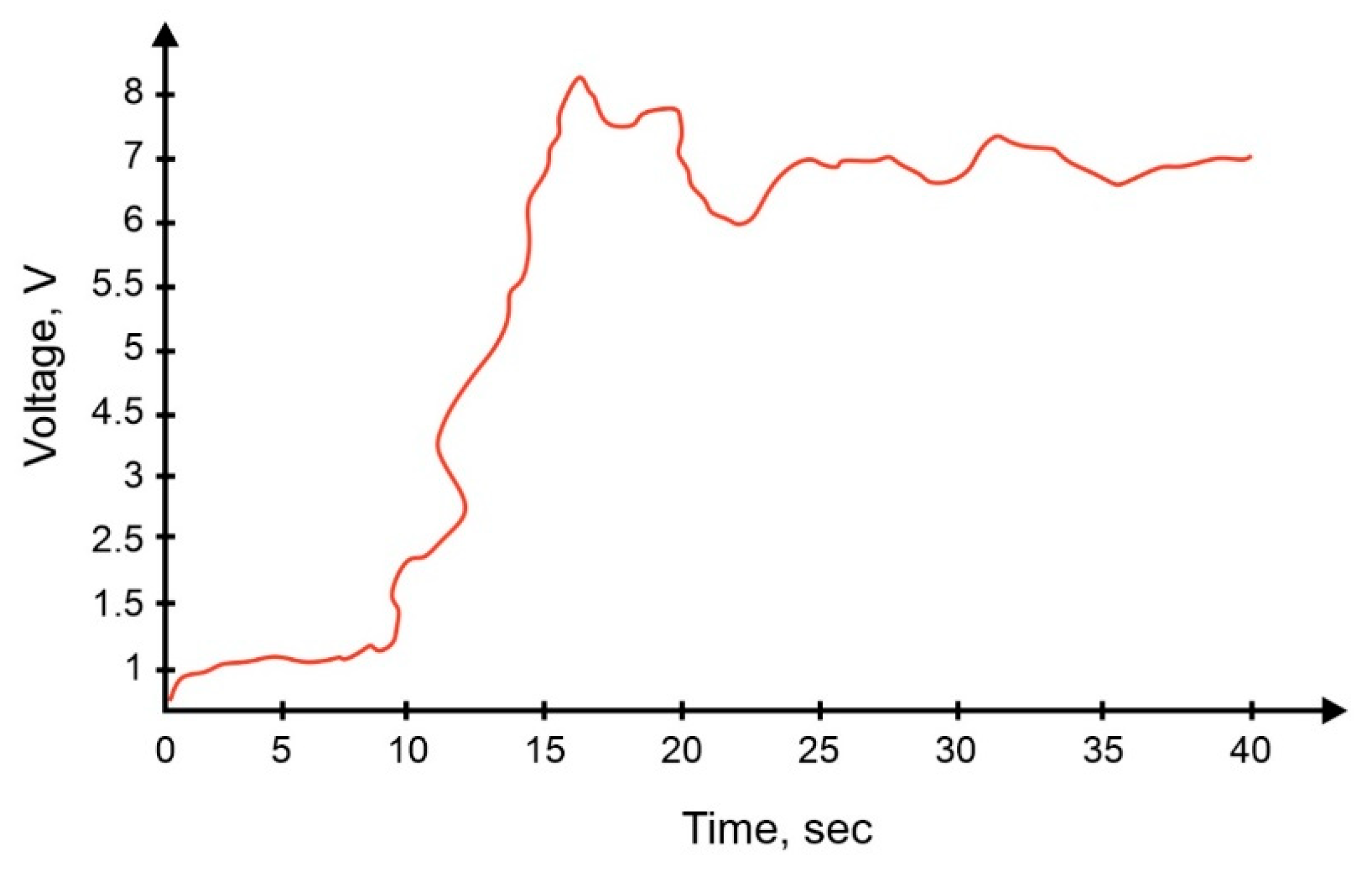
The simulation began with the tuning of terminating resistors and other parameters. That is shown in the example in Figure 12 below.
The simulation result is a signal shape corresponding to the given parameters. It is possible to run a series of simulations performed for different values of given elements, resulting in a set of graphs showing signal forms for different cases. This allows the designer to determine the optimal value for each element. Examples of the outcomes of such modeling are shown in the figures below (Figure 13).
Since knowledge of the signal form alone is not sufficient in each case, further analysis and calculations can be performed. For example, one of the most important properties of variable signals is their frequency spectrum. Given the signal form obtained from the simulation, it is possible to determine such a spectrum and present it on the corresponding graph. An example of such a graph is shown in Figure 14.
The advanced IT tools that make it possible to perform the simulations described are also equipped with other functions that allow further processing of the results and their interpretation. Signal forms can also be analyzed manually in a similar way as if they were using a real system and an oscilloscope. Below is an example illustration showing how to measure the time between two specific signal points (Figure 15).
Routing impedance analysis.
As described above, the implementation of the stated simulations causes the synthesis of printed circuit board techniques, for the calculations accordingly provide for the physical features contemplated in the connections between components. One of the especially necessary properties is the ratio of the parameters and values of the parameters of the scale of the established contour, material dimensions, correlation with other contours and other material features of the board.
The synthesis impedance between the source and the receiver of the provided signal has a major property for the operation of the control line. The option shown above of the absence of locking resistors or the incorrect selection of their value at certain points can lead to a number of negative consequences. However, even with properly selected properties of the source and receiver itself, such unnecessary results can be found in the electrical connection between them.
A mismatched PCB trace impedance can lead to incorrect power transfer from the receiver to the signal line and from the signal line to the receiver. In addition, gross changes in impedance in half of the path due to its shape (e.g., bends, loops) can lead to reflections within the path before they reach the receiver. As a consequence, a portion of the signal's electrical energy can be returned back to its source, and the receiver can not only receive a signal with a reconfiguration and a reduced level, but after repeated reflections at the line boundaries, the receiver can receive repeated renewals of the same signal shifted in time.
The correct calculation of the impedance of the provided electrical connection is in many cases infinitely difficult, if not impossible. On the other hand, due to the use of broad physical models, suitable modeling allows the impedance to be established with a high degree of probability. As mentioned above, the results of all simulations and in-kind analysis are ultimately likely to be verified using the present device, hence the performance accuracy gained from the simulation also affects the state.
The actual application of simulation to find the multiobjective synthesis impedance is mostly possible for conditional cases.
When the entire shape of the printed tracks is assigned by other conditions, then it is possible to choose the values of the components of the electronic circuit in such a way that the entire signal line, starting from the beginning and the signal receiver, operates exactly at a given path, the impedance of which is equal to the sum of the established peak shape.
The selection of the value of one or more components is possible in a way similar to that shown earlier - through the analysis of signal integrity. Although a significant difference seems to be the establishment in the modeling of the physical qualities of printed circuit boards.
The illustrations below show a group of graphs representing the waveforms of the signal under consideration for various values of one of the linear path elements of the provided signal. The graph presented in Figure 16, shows the signal shape for the initial, spurious value of a given element. Unnecessary damped oscillations appearing after any signal front are noticeable. The graph presented in Figure 17, shows the movement of the same signal for the second value of the element in question. As you can see, unnecessary vibrations are eliminated.
The environment in which the numerical calculations were carried out has important information for determining the path parameters. Since the impedance property is conditioned based on the input parameters, the reverse operation is also likely - based on the value of the impedance set by the designer, it is possible to be conditioned by one of the other parameters of the path shown. As a rule, most of them are determined by other constraints, such as the thickness of the laminate, its dielectric constant, or the nature of the track itself, and the only parameter that is freely changed is its width.
4. Discussion
An increasing number of high-speed standards and protocols define basic layout topics for today's PCB designers. Serial standards include Universal Serial Bus, PCIe Gen1 and PCIe Gen2, Gbps Ethernet], LVDS, Serial RapidIO® (SRIO), Common Public Radio Interface (CPRI), Serial Digital Interface SD/HD/3G/ASI (SDI), XAUI and reduced XAUI (XAUI), High/High, SATA/SCSI with serial connection (SAS), GPON, SerialLite II, Fiber Channel, SONET/SDH, Interlaken, many others. All the latest standards combine today's high-speed devices with the highest impermeability either within a single board (chip-to-chip), or in a multi-board implementation within a single machine, or in a machine-to-machine (M2M) scenario.
Many parameters of the microcontroller have a decisive influence at the complexity of the software. Overcomplicating software increases the likelihood of errors in it. That is why the microcontroller was chosen to have a 32-bit architecture and initially support floating-point operations over real numbers in accordance with the IEEE-754 standard.
The advantage of this development is the combination in one integrated circuit of both the processor core (CPU) and the memory of data and programs, peripheral systems that are intermediaries in the flow of information between the cpu unit and the microcontroller environment, as well as specialized diagnostic systems that can be used to identify incorrect operation of the microcontroller and take appropriate measures to eliminate it.
The constructed system is an embedded real-time system, which is most appropriately used for a high-performance single-chip microcontroller.
Investigated module modeling in a specialized program Altium Designer. With the help of this program, potential problems were found, such as the occurrence of crosstalk between paths, the exact values of some elements, accurate analytical calculation.
The proposed design of the measuring system ensures the voltage polarization of the receiving diode with almost zero bias current (bias). This solution will significantly improve the processing characteristics of the proposed system, improving its linearity, and will also allow operation at very low values of the dark current of the photodiode. Reducing these settings will greatly reduce the problems associated with leakage current error, increased noise, and gain peaks caused by random capacitance. An additional advantage of the proposed circuit is a low supply current of about 400 µA.
Without proper protective devices, these devices can be destroyed immediately when overloaded. The design of the power supply can be reasonably affected more seriously than expected.
The developed scheme of the transmitting and receiving module, which is additionally equipped with a preliminary protection and filtering system. 5 V, 12 V and 3.3 V power supply units were also developed.
Investigated module modeling in a specialized program altium designer. With the help of this program, potential problems were found, such as the occurrence of crosstalk between paths, the exact values of some elements, accurate analytical calculation (Figure 10, Figure 11, Figure 12 and Figure 13.). It is also possible to define the rules by which the simulation results will be automatically analyzed. As a result, with every change in the design of the electronic system, it will be possible to automatically simulate and check the integrity of all signals in accordance with the conditions specified by the designer (Figure 8 and Figure 9.).
The final result of the work is the developed circuits, circuit boards and prototype solutions for both systems, as well as the design of a supervisory control system using a microcontroller and complete power paths for each of the developed modules (Figure 6 and Figure 7).
However, even with well-chosen properties of the source and receiver themselves, such undesirable effects can occur within the electrical connection between them.
Improperly matched pcb trace impedance can result in incorrect electrical power transfer from the receiver to the signal line and from the signal line to the receiver. In addition, sharp changes in impedance in the middle of the path due to its shape (e.g., bends, loops) can lead to reflections within the path before they reach the receiver. As a consequence, some of the electrical energy of the signal can be recycled back to its source, and the receiver can not only receive a signal with a changed form and reduced level, but after multiple reflections within the line, the receiver can receive multiple repetitions of the same signal, shifted in time.
Accurate analytical calculation of the impedance of a given electrical connection is in many cases extremely difficult, if not impossible. On the other hand, due to the use of extensive physical models, the corresponding simulation allows the impedance to be determined with high accuracy. As described above, the results of all simulations and analyzes must ultimately be verified using a real device, so the correctness of the values obtained from the simulation is also verified in real conditions.
5. Conclusions
Developed internal data transfer between the measuring unit and peripheral systems and RAM is possible using the built-in hardware DMA controller (Direct Memory Access Controller) with at least 16 channels. Integrated peripheral systems should allow maximum unloading of the CPU block in terms of tasks related to the exchange of data between the processors of the ignition system, the remote control and the diagnostic tool. These peripherals must support at least 3 Mbps asynchronous serial communication in accordance with RS-232, RS-422, and RS-485 standards, as well as CAN (Controller Area Network) communication in 2.0A and 2.0 options B.
The selected microcontroller must be designed for applications where maintaining a high level of reliability at all times is an essential requirement.
The developed measuring module uses the STMicroelectronics STM32F446RCT microcontroller (Fig. 6). STM32F4 is a family of 32-bit microprocessors based on the ARM Cortex M3 core. This core features a Harvard architecture and RISC instruction list, and can operate at up to 120 MHz. Each of the STM32 systems consists of a computing core, RAM, flash memory, a debug interface and additional peripherals sufficient to implement the developed measurement module.
Introduced signal integrity analysis, which allows you to check whether the signals present in the device are correctly transmitted between their sources and receivers. Signal integrity analysis is investigated, which is performed in two stages of the device design process. The initial signal integrity analysis is based on the wiring diagram itself. It takes into account the physical properties of electronic components. A complete signal integrity analysis is performed later in the design process when information about PCB design, shapes, and parameters is available.
Investigated the simulation of the module in a specialized program and found potential problems, such as the occurrence of crosstalk between paths, the exact values of some elements, accurate analytical calculation. The routing of the impedance analysis for the parameters of a given connection is investigated, in which the value affects the shape of a given path, its physical dimensions, distance from other paths, and other physical properties of the board.
The work was supported by a grant and funding the Ministry of Science and Higher Education of the Republic of Kazakhstan within the framework of the Project № AP09259547 «Development of a system of distributed fiber-optic sensors based on fiber Bragg gratings for monitoring the state of building structures», Institute Information and Computational Technologies CS MSHE RK. Experimental researches have been carried out in the laboratories of optoelectronics at the Electric engineering and computer sciences faculty of Lublin Technical University.
References
- Chen, G. Simultaneous strain and temperature measurements with fiber Bragg grating written in novel Hi–Bi optical fiber / G. Chen, L. Liu, H. Jia, J. Yu, L. Xu, W. Wang // IEEE Photonics Technology Letters. – 2004. –Vol. 16, № 1. – P. 221-223. [CrossRef]
- Goncharenko, I. Optical fibre sensors for structural monitoring / I. Goncharenko // Proceedings of Humboldt-Kolleg «Philosophy of Science», –11, 2010. – Odessa, Ukraine. – P. 64-66. 8 September.
- Hill, K.O. Photosensitivity in optical fibers / K.O. Hill, B. Malo, F. Bilodeau, D.C. Johnson // Annual Review of Material Science. – 1993. – Vol. 23. – P. 125-157.
- Morey, W.W. Photoinduced Bragg gratings in optical fibers / W.W. Morey, G.A. Ball, G. Meltz // Optics & Photonics News. – 1994. – Vol. 5. – P. 8-14.
- Glisic, B. Monitoring a subterranean structure with the SOFO® system / B. Glisic, M. Badoux, J.P. Jaccoud, D. Inaudi // Proceedings of the 1st International Conference Long Road and Rail Tunnels. – 2000. – Basel, Switzerland. – P. 127-136.
- Kisala P.; Optoelectronic sensor for simultaneous and independent temperature and elongation measurement using Bragg gratings; Przeglad Elektrotechniczny, Vol.11a, 343–346, 2012.
- Wen X., Zhang D., Qian Y., Li J., Fei N.; Improving the peak wavelength detection accuracy of Sn–doped, H2–loaded FBG high temperature sensors by wavelet filter and Gaussian curve fitting; Sensors and Actuators A–physical, Vol. 174, 91 ̶95, 2012.
- Peng H., Su Y., Ye Z., Zhou B.; A novel fiber Bragg grating sensor for weak pressure measurement based on the Stokes parameter; Optical Fiber Technology, 18(6), 485–489, 2012.
- An J., Liu T., Jin Y.; Fiber optic vibration sensor based on the tilted fiber Bragg grating; Advances in Materials Science and Engineering, Vol. 2013, 1–4, 2013 https://www.researchgate.net/publication/258395214_Fiber_Optic_Vibration_Sensor_Based_on_the_Tilted_Fiber_Bragg_Grating.
- Makovec A., Berruti G., Consales M., Giordano M., Petagna P., Buontempo S., Breglio G., Szillasi Z., Beni N., Cusano A.; Radiation hard polyimide–coated FBG optical sensors for relative humidity monitoring in the CMS experiment at CERN; Journal of Instrumentation, Vol. 9, 2014 https://www.researchgate.net/publication/263036256.
- Song L., Fang F., Zhao J.; Study on viscosity measurement using fiber Bragg grating micro–vibration; Measurement Science and Technology, Vol. 24, 2013.
- Kisala P.; Detection of material defects with indirect method by determining the linear expansion with FBG sensor; Przeglad Elektrotechniczny, R. 89 NR 1a, 29–3, 2013. https://www.researchgate.net/publication/289848280_Detection_of_material_defects_with_indirect_method_by_determining_the_linear_expansion_with_FBG_sensor.
- Luo B., Zhao M., Zhou X., Shi S., Han X., Wang Y.; Etched fiber Bragg grating for refractive index distribution measurement; Optik– International Journal for Light and Electron Optics, Vol. 124, 2777 ̶2780, 2013 https://opg.optica.org/ol/abstract.cfm?uri=ol-42-9-1684.
- “IEEE Std C37.119 –2016 (Revision of IEEE Std C37.119 – 2005), ” in IEEE Guide for Breaker Failure Protection of Power Circuit Breakers, pp. 1 –73, 2016.
- H. C. Lin, B. R. He, H. C. Zo, and K. C. Hsiao, “Development of fast electronic over-current protection circuit using current-adjustable sensing method, ” Advances in Mechanical Engineering, vol. 10, no. 4, 2018. https://www.researchgate.net/publication/324749801_Development_of_fast_electronic_over-current_protection_circuit_using_current-adjustable_sensing_method.
- Abirami and M. L. George, “Electronic circuit breaker for overload protection, ” in 2016 International Conference on Computation of Power, Energy Information and Commuincation (ICCPEIC), pp. 773–776, Tamilnadu Chennai, India, April 2016.
- Jiali An, Tao Liu, and Yongxing Jin Fiber Optic Vibration Sensor Based on the Tilted Fiber Bragg Grating Hindawi Publishing Corporation Advances in Materials Science and Engineering Volume 2013, Article ID 545013, 4 pages. https://www.scopus.com/sources.uri. [CrossRef]
- Singh Ya., Sanjeev K. R., Om Prakash Pankaj K. S. Design and development of tilted fiber Bragg grating (TFBG) chemical sensor with regression analysis of grating parameters for sensitivity optimization. Optical and Quantum Electronics volume53, №: 664 (2021) https://www.scopus.com/sources.uri.
- Chung-Ru Ch., Wei-Lun L., Tsair-Chun L. Design and Testing of a 2D Optical Fiber Sensor for Building Tilt Monitoring Based on Fiber Bragg Gratings. Appl. Syst. Innov. 2017, 1, 2. https://www.researchgate.net/publication/321451299_Design_and_Testing_of_a_2D_Optical_Fiber_Sensor_for_Building_Tilt_Monitoring_Based_on_Fiber_Bragg_Gratings . https://www.scopus.com/sources.uri. [CrossRef]
- J. Boek, S. J. Boek, S. Kersten, P. Kind, P. M¨ attig, L. P¨ ullen1 and C. Zeitnitz Prototypes for components of a control system for the ATLAS pixel detector at the HL-LHC. IOP Publishing Ltd and Sissa Medialab srl. https://www.researchgate.net/publication/258309896_Prototypes_for_components_of_a_control_system_for_the_ATLAS_pixel_detector_at_the_HL-LHC . https://www.scopus.com/sources.uri. [CrossRef]
Figure 1.
Main power source-system of protection and filtration.
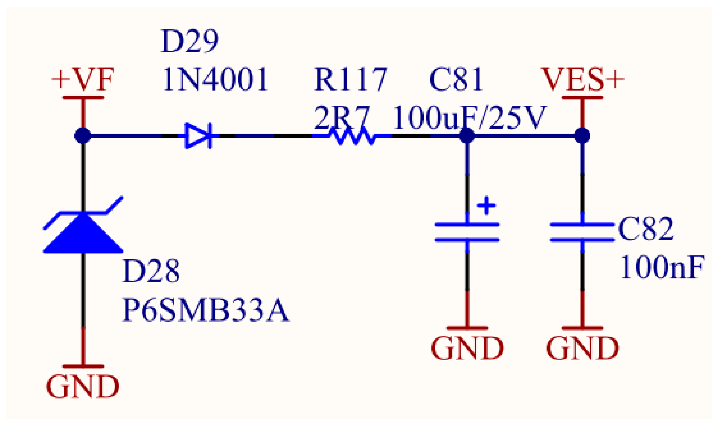
Figure 2.
Power supply unit 12 В.
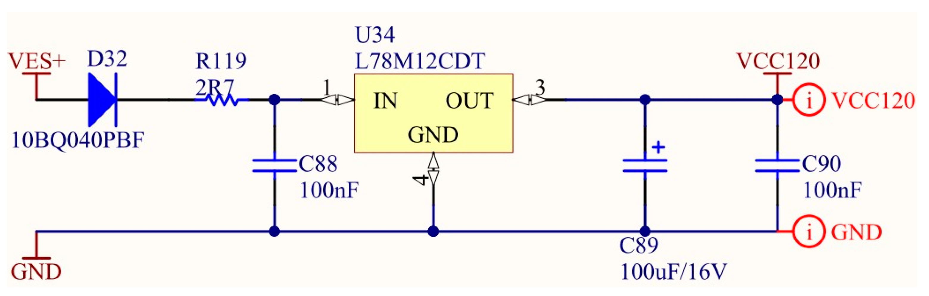
Figure 3.
Power unit 5V.
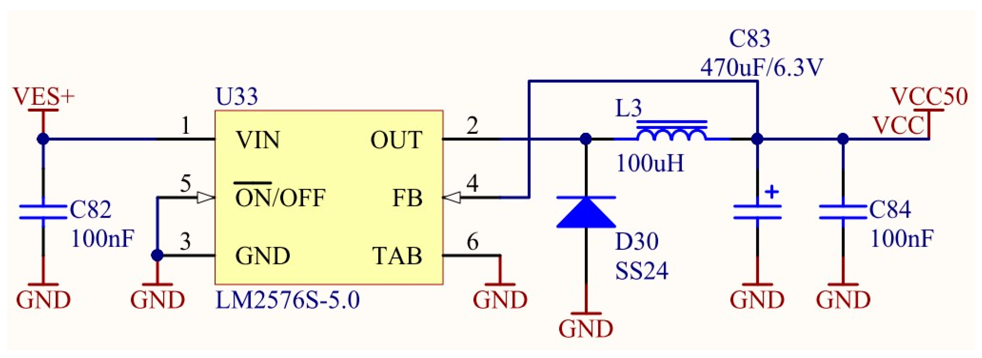
Figure 4.
Power supply unit 3,3V (one section).
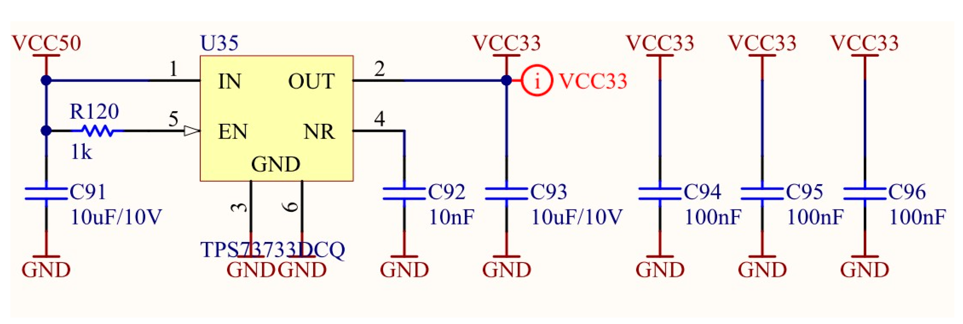
Figure 5.
The binary form of a single precision real number according to IEEE-754.
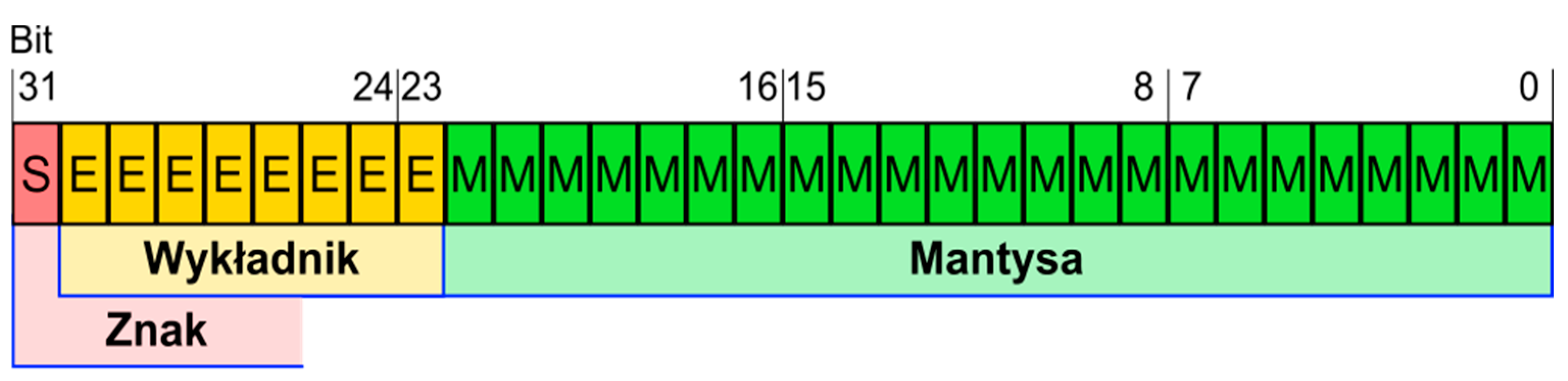
Figure 6.
The selected microcontroller with control and measuring signals connected to it.
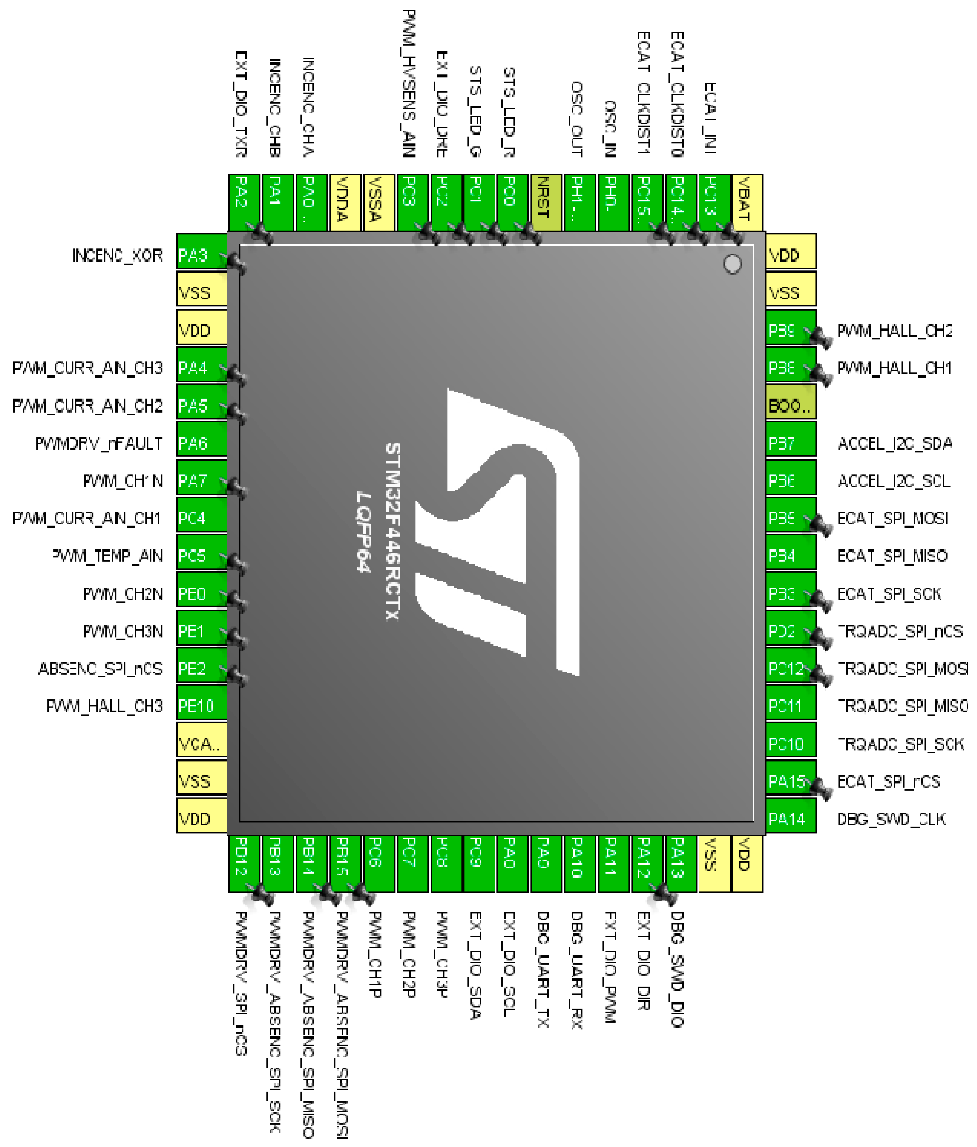
Figure 7.
The selected microcontroller with control and measurement signals connected to it ‒ electronic circuit.
Figure 7.
The selected microcontroller with control and measurement signals connected to it ‒ electronic circuit.
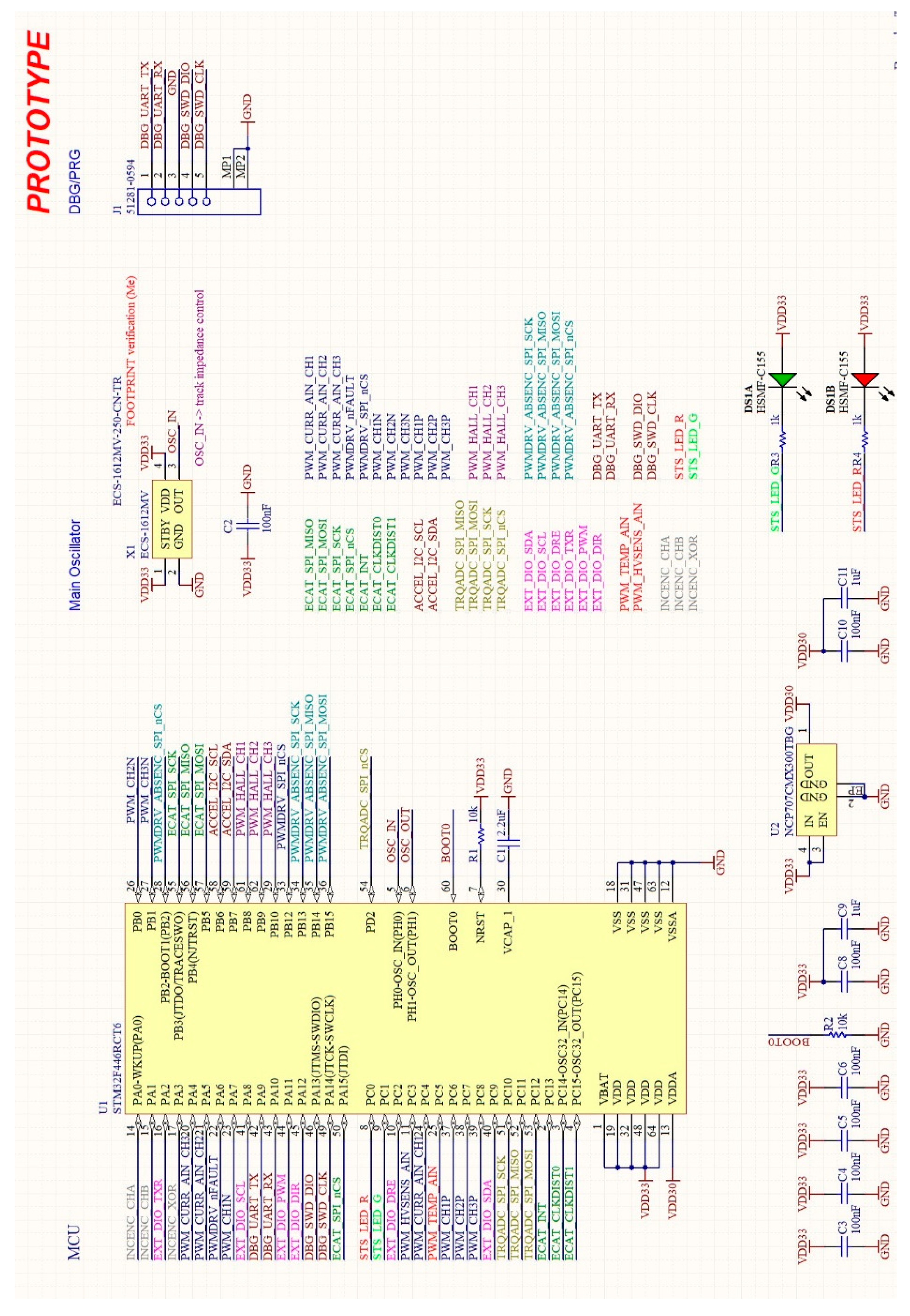
Figure 8.
Definition of a square signal.
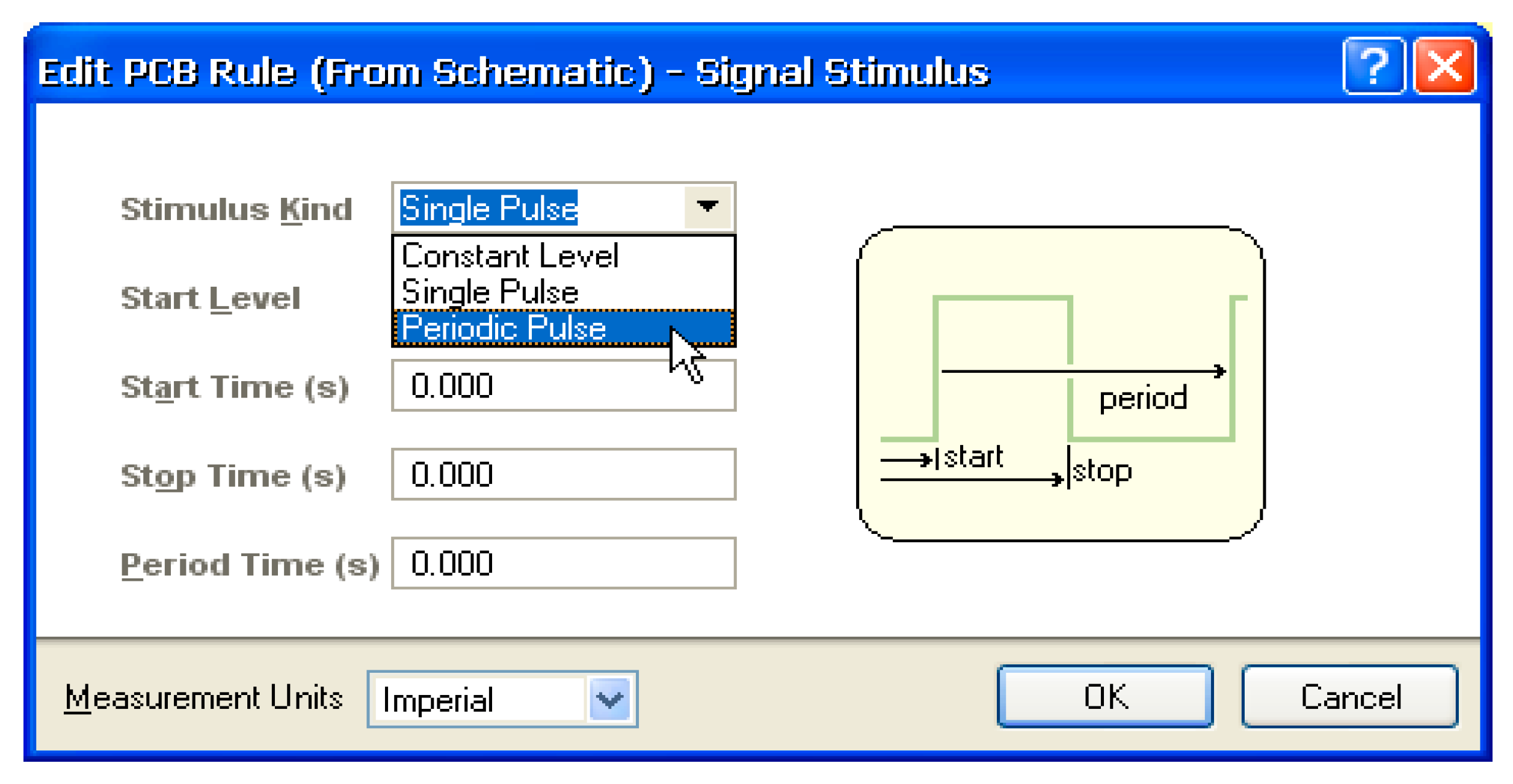
Figure 9.
Determination of the permissible level of exceeding the correct signal value after the appearance of a falling front.
Figure 9.
Determination of the permissible level of exceeding the correct signal value after the appearance of a falling front.
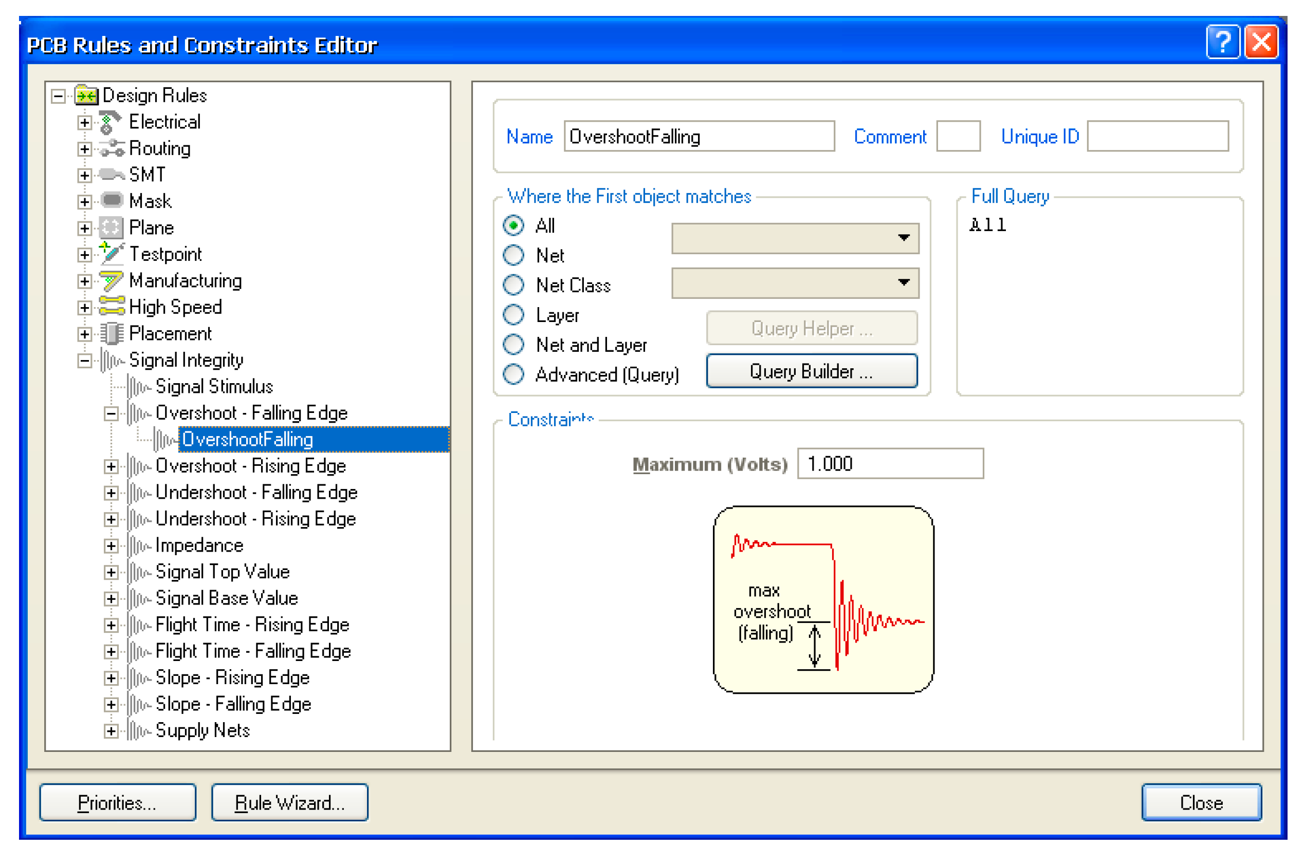
Figure 10.
Outcomes of automatic analysis of simulation outcomes.
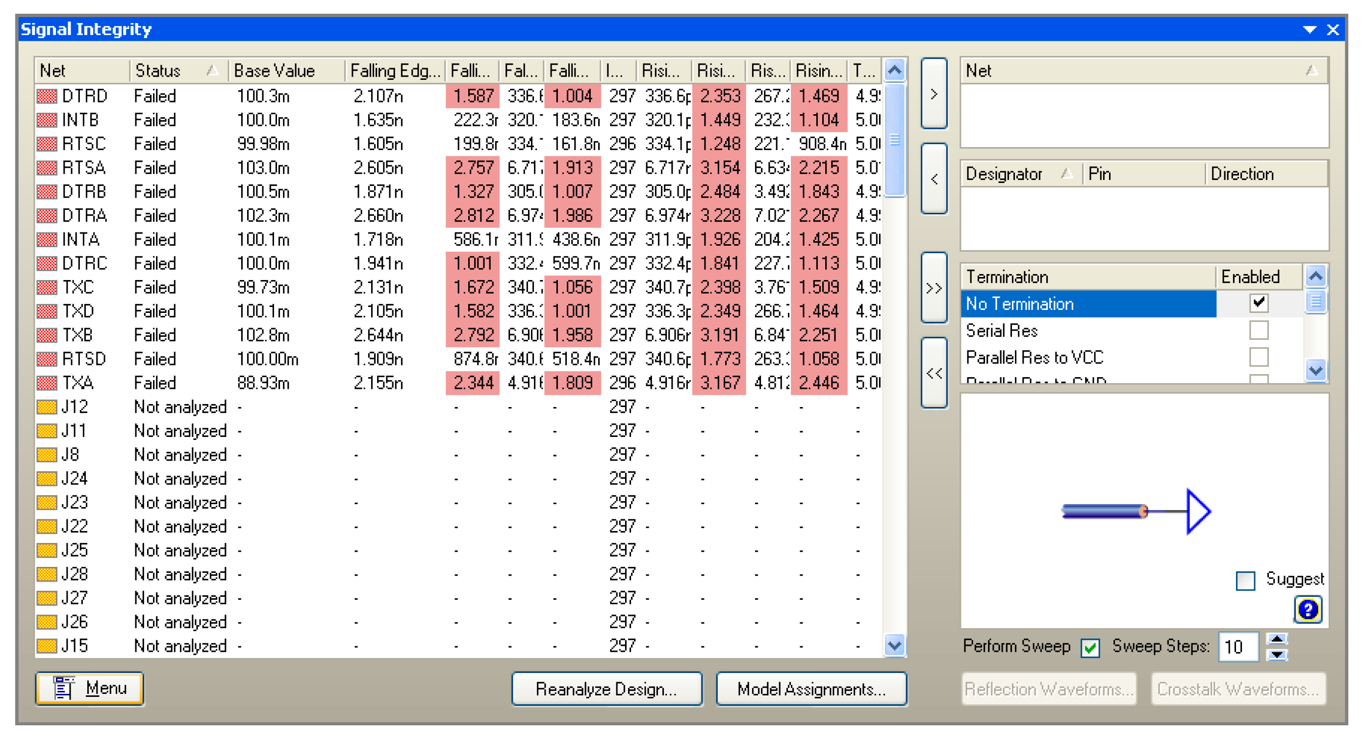
Figure 11.
Detailed information about simulation results for a given signal.
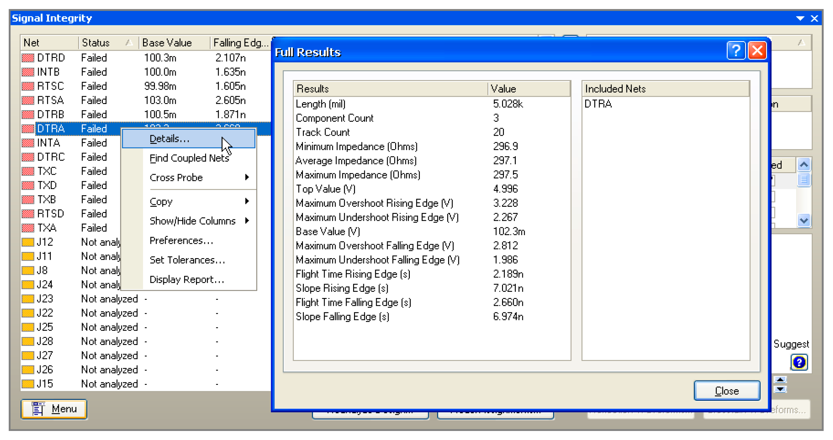
Figure 12.
Example of terminating resistors configuration.
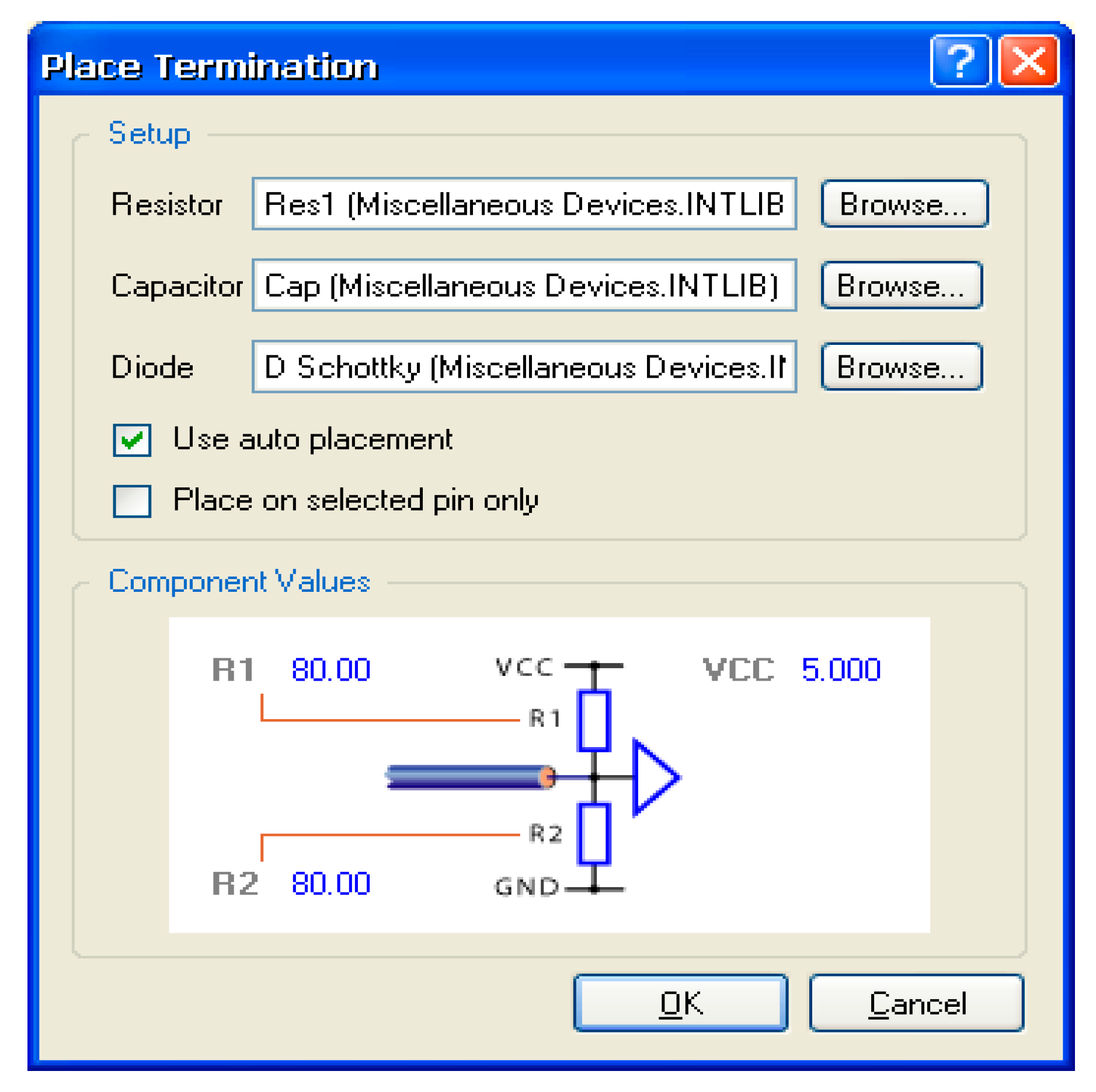
Figure 13.
Series of oscillograms of signals obtained with different ratings of electronic components.
Figure 13.
Series of oscillograms of signals obtained with different ratings of electronic components.
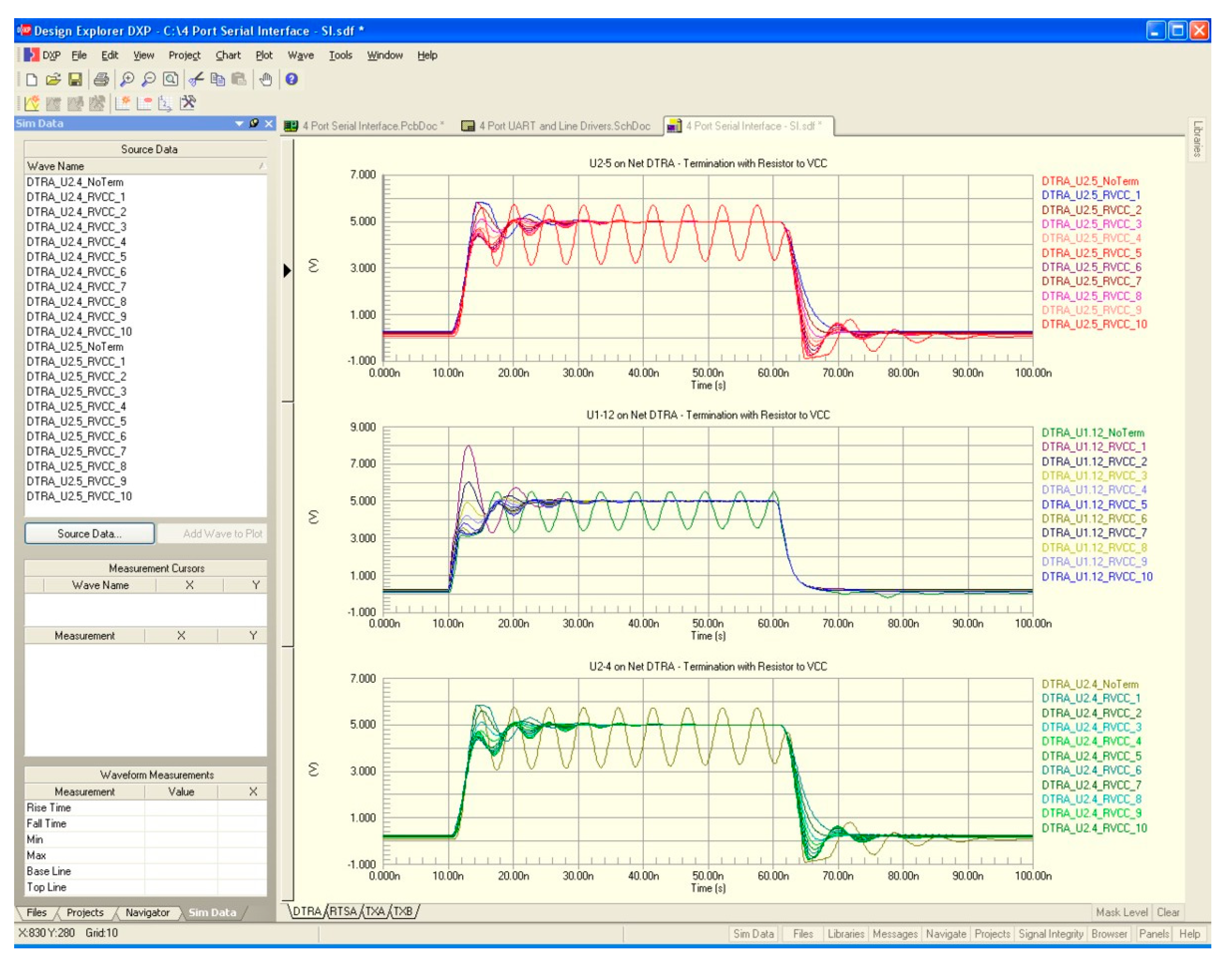
Figure 14.
Modeling signal spectrum.
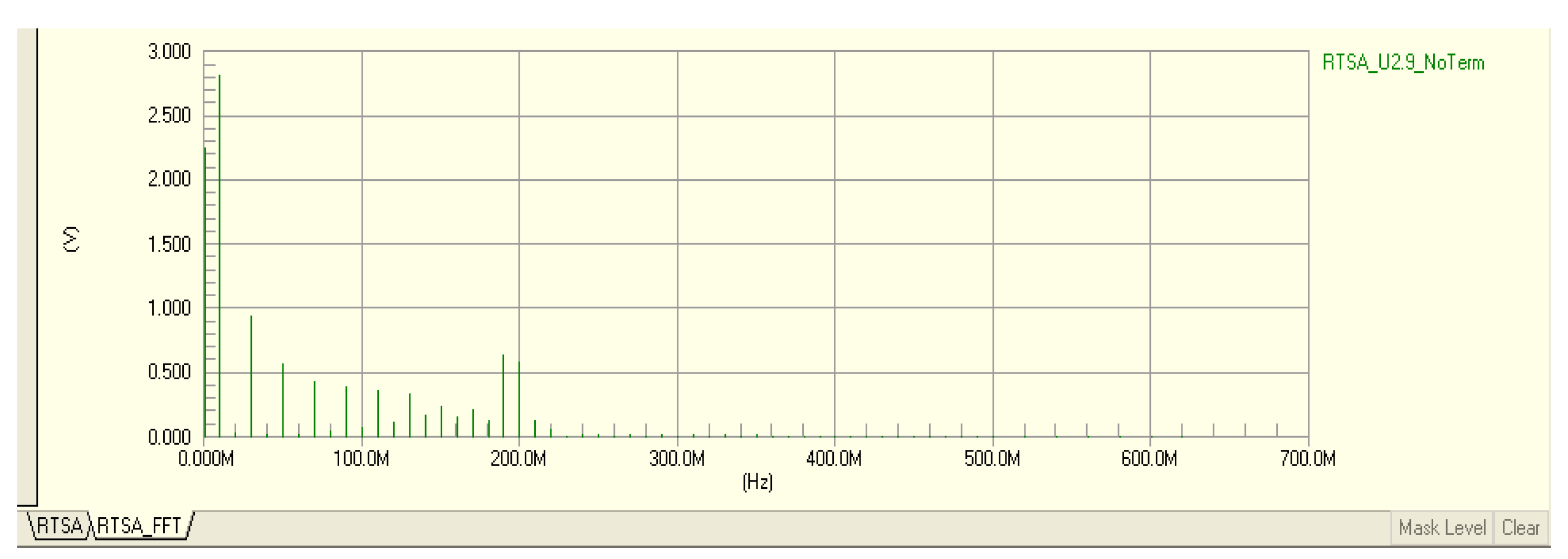
Figure 15.
Measuring the duration of a fragment of the oscillogram of the signal under test.
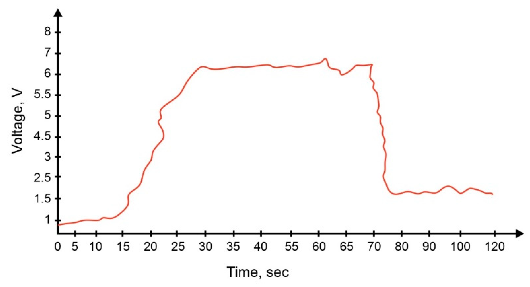
Figure 16.
The signal shape for the initial, spurious value of a given element.
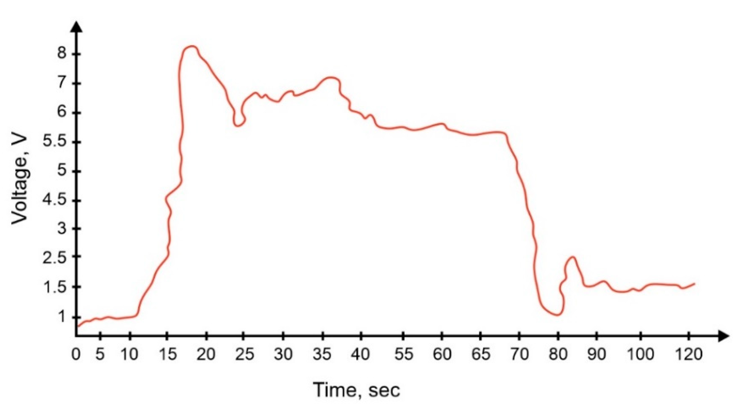
Figure 17.
The movement of the same signal for the second value of the element in question.
Disclaimer/Publisher’s Note: The statements, opinions and data contained in all publications are solely those of the individual author(s) and contributor(s) and not of MDPI and/or the editor(s). MDPI and/or the editor(s) disclaim responsibility for any injury to people or property resulting from any ideas, methods, instructions or products referred to in the content. |
© 2023 by the authors. Licensee MDPI, Basel, Switzerland. This article is an open access article distributed under the terms and conditions of the Creative Commons Attribution (CC BY) license (http://creativecommons.org/licenses/by/4.0/).
Copyright: This open access article is published under a Creative Commons CC BY 4.0 license, which permit the free download, distribution, and reuse, provided that the author and preprint are cited in any reuse.


