Preprint
Article

A Comprehensive Study on the Effect of Defects on Perovskite Solar Cell Performance

Altmetrics

Downloads

496

Views

92

Comments

0

Submitted:

05 June 2023

Posted:

05 June 2023

You are already at the latest version

Alerts
Abstract
This paper focuses on the impact of defects density and carrier capture cross-section area in the electron transport material (ETM), hole transport material (HTM), and absorber layers on the performance of perovskite solar cells and quantum efficiency (QE). Furthermore, the impact of defects density at the interface between ETM/absorber and absorber/HTM is also studied. SCAPS-1D software is used in the current study in determining solar cell performance. The proposed perovskite solar cell structure is a planar FTO/TiO2/ CH3NH3PbI3/ Cu2O. The results indicated that increasing the defect density in the absorber layer significantly affects cell performance, while in ETM and HTM layers, the cell parameters remain unaffected. It is also found that the defect capture cross-section has a similar behavior to the defect density in the main layers (ETM, absorber, and HTM). In addition, it is observed that by increasing the defects density in the ETM/absorber and absorber/HTM interfaces layer, the cell parameters FF, Jsc, and PCE have been slightly decreased, with no effect on Voc. Moreover, it is also noted that the quantum efficiency QE is sharply reduced. Finally, this paper introduced the correlation between the defect density and the capture cross-section, which is the first attempt to find such a relationship in perovskite solar cells to the knowledge of the authors.
Keywords: 
Subject: Engineering  -   Energy and Fuel Technology

1. Introduction

Hybrid mix halide perovskite solar cells (PSC) have risen to prominence due to the unique properties of the absorber, such as elevated charge carriers’ mobility, wide and high absorption coefficients, long carrier diffusion duration, and low electron-hole binding energy, low cost, and ease of manufacturing [1,2]. PSCs have imposed them-selves as an important photovoltaic (PV) technology, competing with silicon-based cadmium telluride solar cells and copper indium gallium selenide solar cells [3]. This remarkable advancement in efficiency PCEs is largely a result of architectural optimization, the application of interface engineering, the development of electron and hole transport components, and the improvement of fabrication processes using elevated-quality perovskite films [4]. Over the last few years, a new group of solar cells based on perovskites with mixed halides has emerged at an unprecedented rate. In 2009, it was discovered that perovskite substances exist in solar panels with a power conversion efficiency (PCE) of no more than 4% [5]. Perovskite materials, such as methylammonium lead iodide (MAPbI3), exhibit a variety of intrinsic defects due to vacancies, antisites, and interstitial defects. Numerous studies have investigated the effect of defect density on the efficiency of hybrid mixed perovskite solar cells [6]. How-ever, no exhaustive study is available at this moment that fully studies the impact of defects taking into account all aspects. A thorough understanding is thus required to make Perovskite solar cells competitive with conventional solar cell technology. Classification of defects is possible according to their position in the band gap energy, where they can be discovered at either a deep level or shallow level [6]. SCAPS-1D software package was used to study the effect of defects density of the active layer and n/i interface of PSCs as a function of cell thick-ness [7]. Au/PEDOT: PSS/Perovskite/CdS/TCO/Glass was used to define the planar p-i-n configuration, and its performance was simulated where a power conversion efficiency of >25% can be achieved. It was discovered that defects density harms the performance of PSCs. The im-pact of the defect in the CH3NH3PbI3 layer was deter-mined using optical and structural properties analysis and structure as FTO/WO3/CH3NH3PbI3/Spiro-OMeTAD/Au [8]. The absorber layer thickness has been changed to determine the optimal cell parameter values. The purpose of this paper is to examine the impact of defects in the PSC structure on the following: Glass/FTO/TiO2/CH3NH3PbI3/Cu2O/metal back contact, which is simulated using the solar cell one-dimensional capacitance simulation (SCAPS-1D). The work investigates the effect of defects on the performance of the PSC and the quantum efficiency QE, with a particular emphasis on the capture cross-section area and defects density in the ETM and HTM, and absorber layers as well as in the interface layers. In addition, the impact of defect level and defect type on quantum efficiency will be studied, and compared the behavior of Cu2O with CuI and Spiro-OMeTAD as HTM material.

2. Device Structure and Parameters

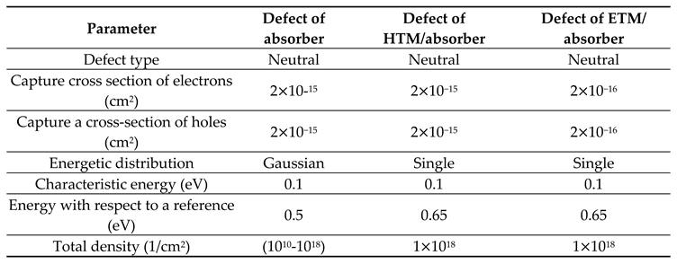
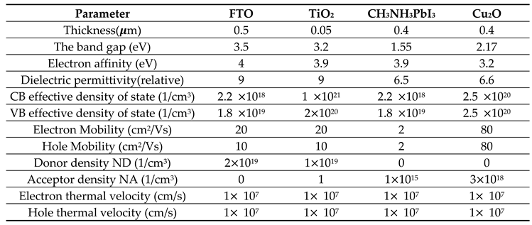
SCAPS 1D program is used in this study since it is wide-ly regarded as among the most efficient and user-friendly simulation tools for modeling solar cells. The proposed perovskite solar cell structure is a planar structure com-posed of glass/FTO/TiO2 (ETM layer)/CH3NH3PbI3 (active layer)/(HTM layer)/metal back contact as illustrated in Figure 1. The simulation parameter values are listed in Table 1 based on data from the literature. The defect parameters of the CH3NH3PbI3 absorber layer and the ETM/absorber and HTM/absorber interface of the PSCs are summarized in Table 2.
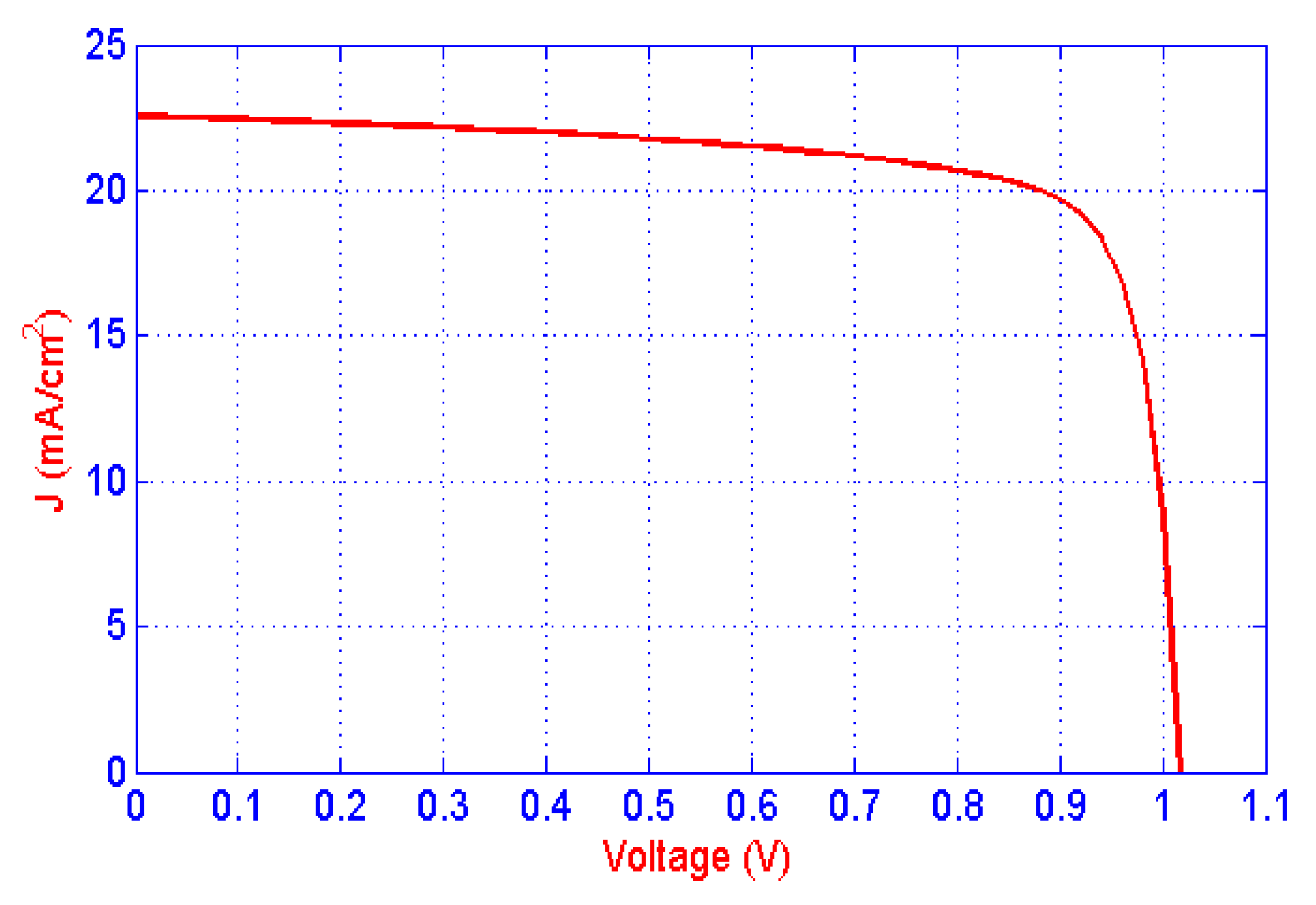
Other parameters include the defects density in the CH3NH3PbI3 layer, which is set to (2.5×10¹³) cm−3 using a Gaussian energetic distribution, and the defect densities Nt in other layers, which is set to 1015 cm−3 and the absorber coefficient is set to 105 cm−1, while the absorber layer’s absorption α is set to (1.5×10⁵) cm−1 [13]. The simulation makes use of the spectrum generated under standard conditions (air mass AM1.5 G, temperature 300 K). The voltage is ranged between 0 and 1.3 V. The reference cell’s current-voltage characteristics (J-V) based on Cu2O as HTM is shown in Figure 2. The performance parameters for the reference cell that is based on Cu2O and given as PCE = 17.72%, FF =77.23%, Jsc = 22.54 mA∙cm−2, and Voc= 1.01 V.

3. Result

3.1. The Influence of Defect Density in the Absorber Layer with Cu2O as the HTM Layer

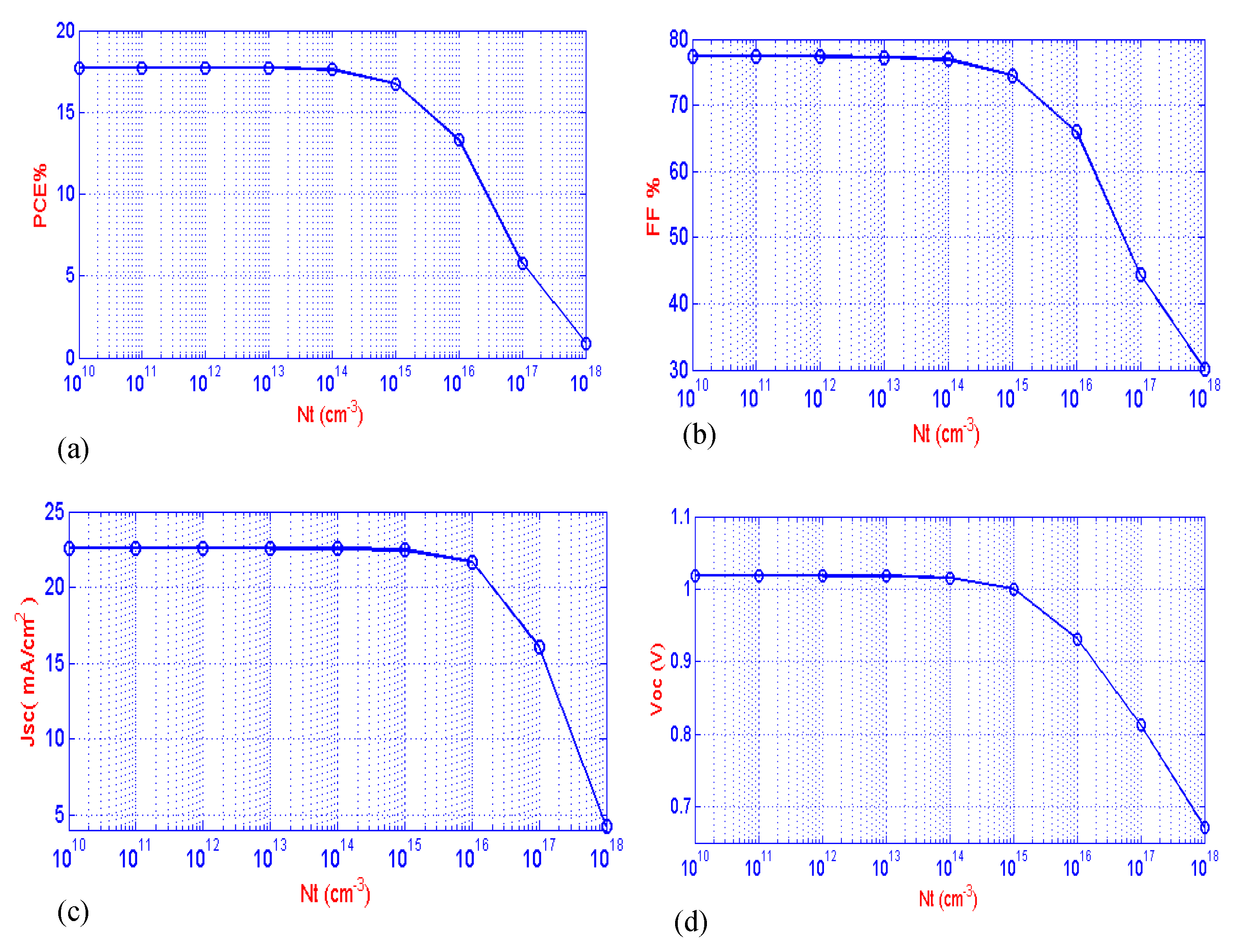
To investigate the effect of defect density in the MAPbI3 layer on performance parameters, the defect density of photovoltaic cells was varied between 2.5×1010 cm−3 and 2.5×1018 cm−3, while maintaining other parameters un-changed such as capture cross-section in absorber layer equals to 2×10⁻¹⁵ cm2. Total density in both interfaces HTM and ETM are set to 1018 cm−2. The defect energy level is set to 0.5 eV above the valance band as shown in Figure 3.
As it is shown in Figure 3a, the PCE dropped rapidly from 17.60 % to 0.86 % with increasing the defects density from 2.5×1015 cm−3 to 2.5×1018 cm−3. Additionally, if the defects density is less than 2.5×1015 cm−3, the PCE keeps the same as the change is about 17.73 %. Furthermore, if the defects density is greater than 2.5×1015 cm−3, the FF falls from 74.47 % to 30.18 % as depicted in Figure 3b. It can also be observed that when the defects density is less than 2.5×1015 cm−3, the FF has remained nearly un-changed at around 77.27%. The Jsc and Voc are presented in Figures 3c and 3d, respectively. It can be observed that the Voc drops from 1.01 V to 0.67 V with increasing the defects density from 2.5×1015 cm−3 to 2.5×1018 cm−3. However, the Voc wasn’t significantly changed when the defects density is lower than 2.5×1015 cm−3. Furthermore, the Jsc falls quickly from 22.45 mA.cm−2 to 4.23 mA.cm−2 as the defect’s density is higher than 2.5×1015 cm−3. How-ever, when the defect density is less than 2.5×1015 cm−3, the Jsc is unchanged at 22.54 mA.cm−2, and the defect density is near the center of the band gap. The increased number of traps had a defects density greater than 2.5×1015 cm−3, due to a significant decrease in Jsc. This is highly consistent with numerous studies, demonstrating that defects in the MAPbI3 absorber layer have a significant effect on the cell’s performance [14,15,16].

3.2. The Effect of Capture Cross-Section in the Absorber Layer with Cu2O as HTM Layer

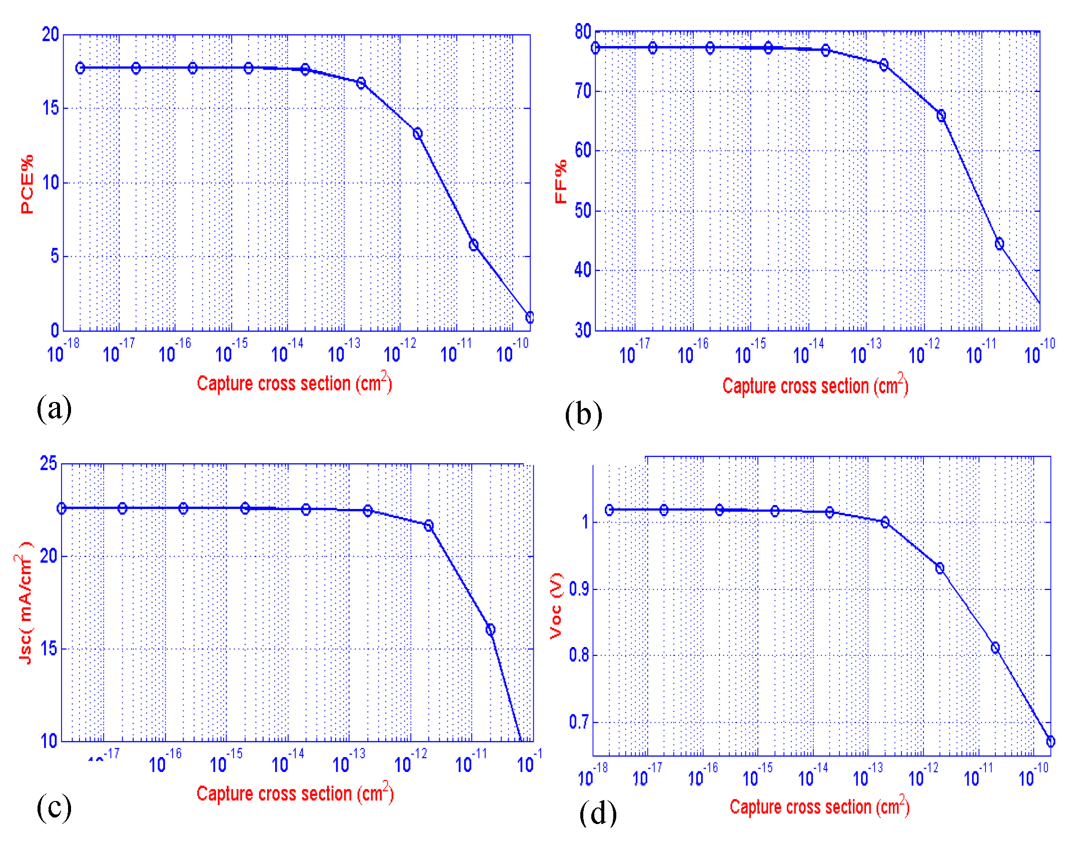
The impact of electron σn and hole σp capture cross-section in MAPbI3 layer on perovskite cell is investigated by varying the capture cross-section area value from 2×10⁻¹⁰ cm2 to 2×10⁻¹⁸ cm2. The defect level is set to 0.5 eV above the valance band, while other parameters are kept constant such as defects density in the absorber layer, which is set to 2.5×1013 cm−3. The total density in both interfaces HTM and ETM are set to 1018 cm−2. The results are illustrated in Figure 4.
As it is shown in Figure 4a, when the value of the capture cross-section area in MAPbI3 is greater than 2×10⁻¹³ cm2, the PCE is reduced sharply from 16.73 % to 0.86 %. In addition, when the capture cross-section area is set to be smaller than 2×10⁻¹³ cm2, the PCE is kept unchanged at 17.73 %. Furthermore, if the capture cross-section is great-er than 2×10⁻¹³ cm2, the PCE is decreased to about 0.86 %. The change of FF versus the capture cross-section in the MAPbI3 absorber layer is shown in Figure 4b, where FF varies slightly from 77.27 % to 76.89 %, due to the capture cross-section, which is less than 2×10⁻¹³ cm2. Once the capture cross-section reaches 2×10⁻¹³ cm2, the FF drops rapidly with the increase of the capture cross-section. As with other parameters, it is found that the Jsc changes slightly when the value of the capture cross-section is smaller than 2×10⁻¹³ cm2. The Jsc decreases significantly from 22.45 mA.cm−2 to 4.23 mA.cm−2, as the capture cross-section area increases gradually from 2×10⁻¹³ cm2 to 2×10⁻¹⁰ cm2. At the capture cross-section area of 2×10⁻¹⁰ cm2, the Jsc is approximately 4.23 mA.cm−2. If the capture cross-section in the MAPbI3 layer increases from 2×10⁻¹³ cm2 to 2×10⁻¹⁰ cm2, the Voc decreases from 1.01 V to 0.67 V. In addition, the Voc is kept unchanged when the capture cross-section area is set to be smaller than 2×10⁻¹³ cm2. To describe this theory, it is generally known that the carrier lifetime is strongly dependent on capturing cross-sections and the defect trap density. The capture cross-section depicts the probability of the trap catching the free carried item, thereby increasing the capture cross-section area for electrons and holes resulting in a decrease of a lifetime, as well as efficiency, fill factor, current density, and open circuit voltage. It is a good match to the recent research indicating that defects in the absorber layer have a significant impact on the cell’s performance [17,18]. Increasing the defects density and capture cross- section area within the selected range as it is shown in reference results in cell performance parameters: PCE = 17.72%, FF =77.23%, Jsc = 22.54 mA∙cm−2, and Voc = 1.01V. The increase of the defects density and capture cross-section have shown no impact on the performance parameters of the PSC in HTM and ETM layers. To ex-plain this, the role of the hole transportation layer HTM and electron transportation layer ETM is only to extract and convey the collected holes and electrons from the absorber region. Thus, there will have no significant im-pact.

3.3. The Effect of Defect Density in HTM and ETM Interface Layers

In the suggested structure of the cell, two interfaces were presented: (ETM/absorber) and (absorber/HTM), and the effect of defects density in the ETM/absorber and absorb-er/HTM interface layers on the cell’s performance was examined. The defect parameters for both interface layers are previously summarized in Table 2.
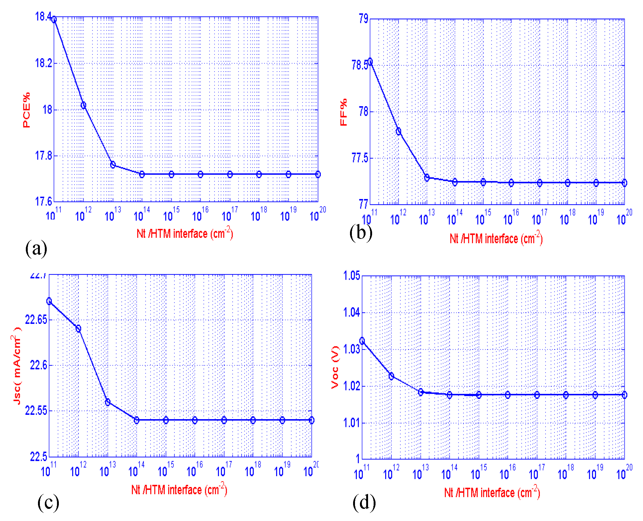
Firstly, the impact of defects density in the HTM/MAPbI3 interface layer on the cell parameters is studied where there was a variation in the defect density from 1011 cm−2 to 1020 cm−2. The defect energy level is set to 0.5 eV above the valance band, while other parameters are kept un-changed such as defect density, which is set to 2.5×1013 cm−3, and the capture cross-sectional in the MAPbI3 layer is set to 2×10⁻¹⁵ cm2. The results are depicted in Figure 5.
As it is shown in Figure 5, the performance parameters changed slightly with the increase in the defect’s density. When the defect densities varied from 1011 cm−2 to 1014 cm−2, the PCE was reduced slightly from 18.4% to 17.74%. Once the defect density reaches 1014 cm−2, the PCE keeps constant at about 17.72%. In addition, when defect density is set to be greater than 1014 cm−2, the FF remains un-changed at about 77.24%. Whereas once the defect density is set to be lower than 1014 cm−2, the FF reduces slightly from 78.54% to 77.29%. Moreover, if the defect density is set to be less than 1014 cm−2, the Jsc decreases slightly from 22.67 mA.cm−2 to 22.45 mA.cm−2 with the increase of the defect’s density. In contrast, the Voc is relatively unchanged and remains around 1.01V with the increase of the defect’s density. It can be observed that the variation of the defects density has an insignificant effect on HTM/MAPbI3 interface layer on perovskite solar cell devices.
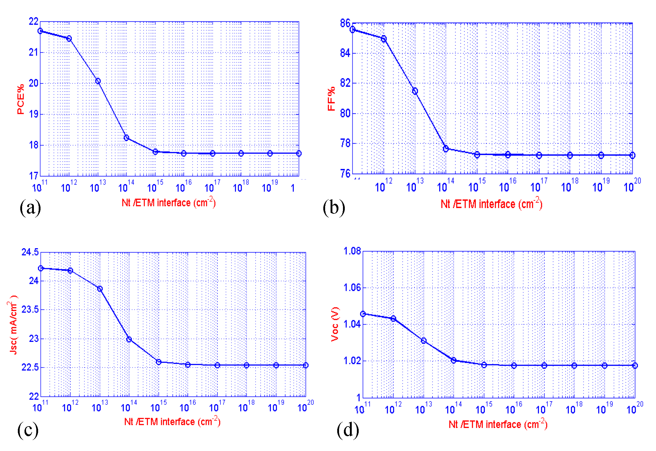
The impact of defect density in MAPbI3/TiO2 interface layer on cells performance parameters PCE, FF, Jsc, and Voc has also been investigated by changing the defect density from 1011 cm−2 to 1020 cm−2. The defect energy level is set to 0.5 eV above the valance band, while other parameters are fixed unchanged such as defect density equal to 2.5×1013 cm−3, and the capture cross-section area in the absorber layer is set to 2×10⁻¹⁵ cm2. The results are shown in Figure 6.
As it is shown in Figure 6, the PCE reduces slightly from 21.68% to 17.73% when the defects density in MAP-bI3/ETM layer increases from 1011 cm−2 to 1015 cm−2. It can also be seen that the PCE has remained unchanged (about 17.72%) when the defects density is set to be higher than 1015 cm−2. The FF decreased slightly to 8.35% when the defect density was below 1015 cm−2. Maximum FF is achieved around 85% when the defects density is set equal to 1011 cm−2. When the defect density is greater than 1015 cm−2, the FF remains constant at about 77.23%. The Jsc in MAPbI3/TiO2 interface is kept unchanged (around 22.54 mA.cm−2) as the defect’s density is set higher than 1015 cm−2. In addition, it can be observed that the Jsc de-clines slightly from 24.22 mA.cm−2 to 22.55 mA.cm−2 when the defects density increases from 1011 cm−2 to 1015 cm−2. In addition, when the defects density varies within the mentioned range, the open circuit voltage Voc remains constant at about 1.01 V. From the result, it can be noticed that the defect density in MAPbI3/ETM interface layer has a trivial impact on PCE, FF, and Jsc, while it does not affect Voc at all. To explain this, the performance of the cells is suffering a slight reduction, due to the ETM and HTM interfaces being described as defects with the increase of the defect’s density within the tested range

3.4. The Effect of Defects Density on Photovoltaic Performance in MAPbI3 Absorber Layer for All Cells

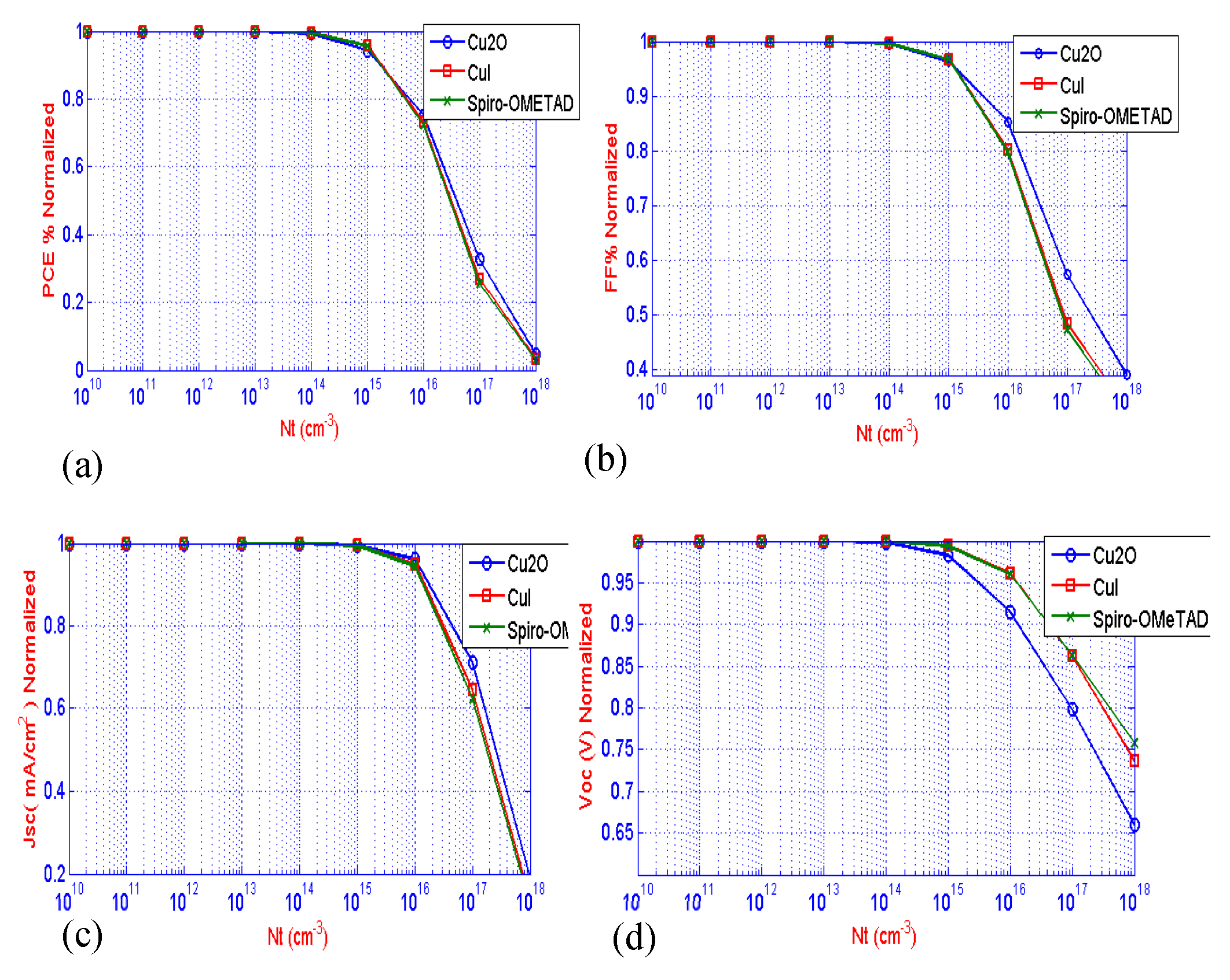
To evaluate the impact of defects density in MAPbI3 layer on cells parameters for different hole transport mate-rial HTM, such as Cu2O, CuI, and Spiro-OMeTAD, normalized results are produced to compare the performance with the existing of each material. This comparison gives a deeper physical insight to understand the impact of changing the HTM layer at different defect densities. The studied defects’ densities varied from 1010 cm−3 to 1018 cm−3. The defect level is set to 0.5 eV above the valance band while maintaining other parameters unchanged, such as capture cross-section in the absorber layer, which is set to 2×10⁻¹⁵ cm2, and the total density in both interfaces HTM and ETM are set to 1018 cm−2. The results are illustrated in Figure 7.
As it is shown in Figure 7, when the defects density is varied within the mentioned range, it can be observed that the normalized PCE falls rapidly once the defect density exceeds 2.5×1015 cm−3. It can be also determined that the normalized PCE is unchanged when the defect density is set to be less than 2.5×1015 cm−3 for all HTM. As defect density in the MAPbI3 absorber layer increases from 2.5× 1015 cm−3 to 2.5×1018 cm−3, the FF reduces sharply. How-ever, the Cu2O as hole transport material has a better performance than CuI and Spiro-OMeTAD, while the Spiro-OMeTAD and CuI have almost a similar behavior under the same condition. In addition, the FF is unchanged when the defect density is less than 2.5×1015 cm−3 for different HTM materials. In contrast, the Jsc drops significantly as the defect’s density is greater than 2.5 ×1015 cm−3 with different HTM materials. Cu2O has better behavior than CuI and Spiro-OMeTAD. The Jsc almost remains constant when the defects density is below 2.5×1015 cm−3 for all HTM materials. Figure 7d shows that when defects density is varied from 2.5×1015 cm−3 till 2.5×1018 cm−3, a slight reduction in Voc is observed for different HTM materials in the MAPbI3 absorber layer and the Spiro-OMeTAD, CuI gives better behavior than Cu2O. However, if the defects density is less than 2.5×1015 cm−3, the Voc is unchanged with all HTM materials.

3.5. The Effect of Defects on Quantum Efficiency with Cu2O as HTM Layer

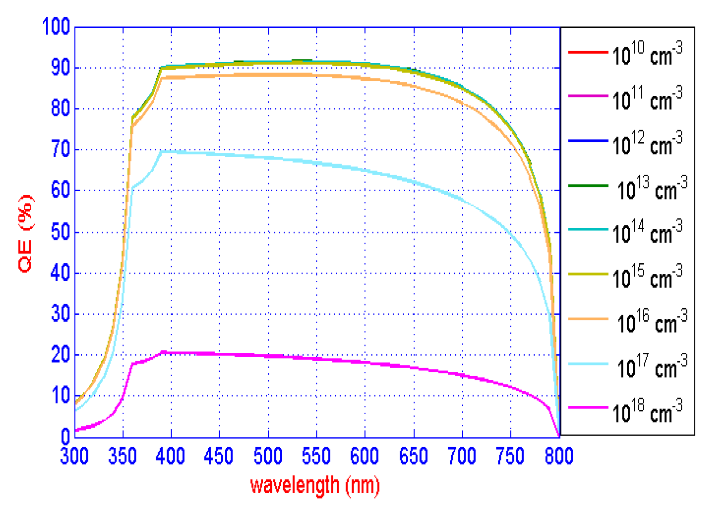
The influence of defect density in the MAPbI3 layer on the quantum efficiency of perovskite solar cells has been investigated by changing defect density from 1010 cm−3 to 1018 cm−3 over a range of wavelengths from 300 to 800 nm. The variation of QE with light wavelength at different defect densities is depicted in Figure 8.
It can be observed in Figure 8 that the maximum achieved quantum efficiency is about 90.2% within the wavelength range from 390 nm to 650 nm for defects densities from 1010 cm−3 to 1015 cm−3. Furthermore, the QE declines sharply for defects densities higher than 1015 cm−3 to reach only 20% at an exponential rate. This indicates that the defects density in the CH3NH3PbI3 layer of 1015 cm−3 or lower is enough to absorb most of the incident photons, and the rest does not make a significant contribution to the cell, because the defects density affects the recombination of the photo-generated electron-hole pairs in the active layer (absorber region).
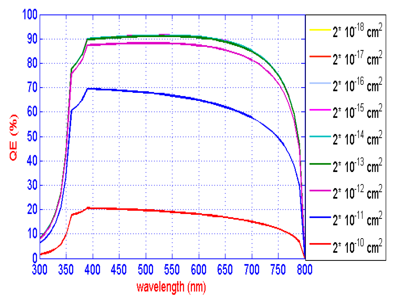
Moreover, the influence of the capture cross-section area in the MAPbI3 layer on the quantum efficiency of PSCs has been studied by varying the capture cross-section area of carriers from 2×10⁻¹⁰ cm2 to 2×10⁻¹⁸ cm2 and computing the QE over a wavelength range from 300 nm to 800 nm as shown in Figure 9.
As it is shown in Figure 9, the maximum quantum efficiency is approximately 90.2 % within the wavelength range of 390 nm to 650 nm, for capture cross-section area varies from 2×10⁻¹⁸ cm2 to 2×10⁻¹³ cm2. Additionally, the QE decreases rapidly, for capture cross-section area values that are greater than 2×10⁻¹³ cm2, eventually reaching only 20% at an exponential rate. The quantum efficiency in-creases rapidly at 300 nm with a capture cross-section area of less than 2×10⁻¹³ cm2. Then the increment slows down when the capture cross-section reaches or is lower than 2×10⁻¹³ cm2. The capture cross-section area of the defects in the MAPbI3 layer is sufficient to improve the performance of PSC cells.

3.6. Break Down Point Determination of Cell Performance in PSC

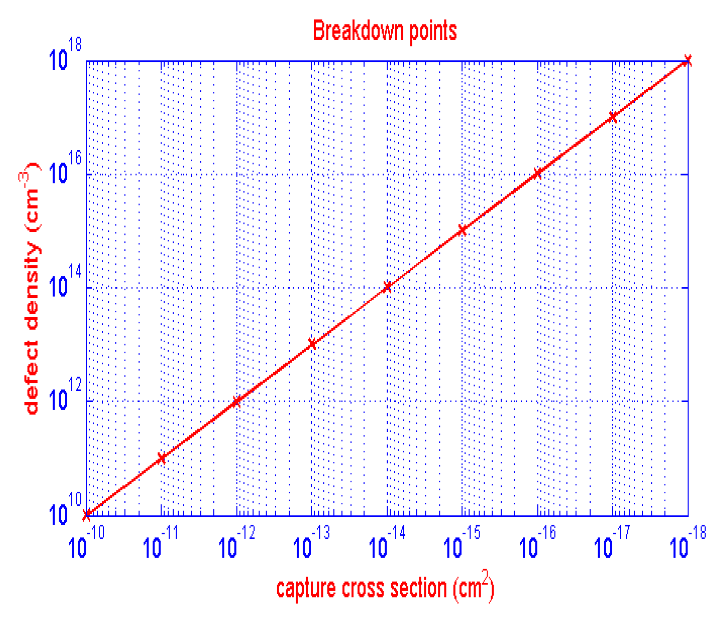
Figure 10 illustrates the linear correlation relationship be-tween the defect density and the capture cross-section area of carriers in the absorber layer. Each point on the red line determines the value of defect density and captures cross-section area of the defect at which the cell performance breaks down. This applies to metal impurities in perovskite solar cells.
The most common impurities in MAPbI3 material are (Au, Cu, Cr, Mo, Co, Ni) [19], where Table 3 shows the capture cross-section area of these metals. These values are taken from the literature [20,21,22,23].
From the results, it can be noticed that the capture cross-section area has a direct significant impact on the solar cell performance. In addition, the defects density has also a strong impact on the performance of PSC. However, it can be found that the value of defect density alone is not sufficient to evaluate the breakdown point of the cell performance without knowing the capture cross-section area of the defect. In contrast, the capture cross-section area alone does not give a clear image of the possible degradation of the cell’s performance without knowing the defect concentration in the material. Thus, there is a strong correlation relationship between the capture cross-section area and the defects density as depicted in Figure 10. This demonstrates the importance of knowing the capture cross-section area along with the defects density precisely to determine the breakdown point of the solar cell. For example, Table 3 it is shown that the electrons capture cross-section area for gold (Au) in CH3NH3PbI3 is 1.4 ×10⁻¹⁶ cm2, which means that the defect density of this impurity (i.e gold) should not exceed 1.4×1016 cm−3 to avoid reaching the breakdown scenario in the performance of the solar cells, while the capture cross-section of electrons for Cu is 1.6×10⁻¹⁸ cm2, poses a lower risk of breakdown than Au, due to that any defect density exceeding 2.5×1018 cm−3 constitutes a breakdown in the solar cell. However, Co, Cr, and Mo are considered to pose a greater risk of breakdown solar cells, which any defect density exceeding 1014 cm−3 results in a performance breakdown. Thus, when the defect density of a solar cell exceeds these limits, the efficiency of the cell will be rapidly decreased.

4. Conclusions

In this paper, the effect of defects concentration and the capture cross-section area of defects in the ETM, HTM, and CH3NH3PbI3 layers were studied. Planer structure FTO/TiO2/CH3NH3PbI3/Cu2O was investigated by using (SCAPS-1D). The impact of defects density and capture cross-section area in the interface layers on the performance of perovskite solar cells have also been studied. The results showed that as the defects density in the CH3NH3PbI3 layer increased, the efficiency, fill factor FF, and Jsc values decreased significantly at defect density Nt greater than 1015 cm−3, while Voc was slightly reduced. Ad-additionally, it was observed that a larger capture cross-section area > 2×10⁻¹⁴ cm2 results in a significantly degraded cell performance and exhibits a defects density effect-like behavior. The cells’ performance parameters Jsc, PCE, and FF were reduced slightly when the defects density at ETM/CH3NH3PbI3 and HTM/CH3NH3PbI3 interface layers varied from 1011 cm−2 to 1014 cm−2 and the results also indicated that the Voc has shown no change. It is demonstrated that the effect of defects density in the interface layer was negligible in comparison to the absorber layer. Moreover, from the result, it can be observed that the quantum efficiency of perovskite solar cells is sensitive to an increased defect density and capture cross-section area in the CH3NH3PbI3 layer, where the quantum efficiency is reduced sharply from 90.2% to 20% at defects density and capture cross-section areas vary from 1015 cm−3 to 1018 cm−3 and from 2×10⁻¹³ cm2 to 2×10⁻¹⁰ cm2, respectively. Finally, this work has introduced, for the first time, a correlation relationship between the defect density and capture cross-section area that determines the breakdown point in the cell performance.

Author Contributions

Conceptualization, Hajar Kh. Ibrahim, Ahmed M. A. Sabaawi and Qais Th. Algwari; methodology, Ahmed M. A. Sabaawi and Qais Th. Algwari; software, Hajar Kh. Ibrahim; validation, Ahmed M. A. Sabaawi and Qais Th. Algwari; formal analysis, Ahmed M. A. Sabaawi and Qais Th. Algwari; investigation, Hajar Kh. Ibrahim; resources, Hajar Kh. Ibrahim; data curation, Hajar Kh. Ibrahim and Ahmed M. A. Sabaawi; writing—original draft preparation, Hajar Kh. Ibrahim.; writing—review and editing, Ahmed M. A. Sabaawi and Qais Th. Algwari; supervision, Ahmed M. A. Sabaawi and Qais Th. Algwari. All authors have read and agreed to the published version of the manuscript.

Funding

This research received no external funding.

Conflicts of Interest

The authors declare no conflict of interest.

References

  1. J. Huang, Y. Yuan, Y. Shao, and Y. Yan, “Understanding the physical properties of hybrid perovskites for photovoltaic applications,” Nat. Rev. Mater., vol. 2, (2017). [CrossRef]
  2. H. J. Snaith, “Present status and future prospects of perovskite photovoltaics,” Nat. Mater., vol. 17, no. 5, pp. 372–376, (2018). [CrossRef]
  3. D. Yang, Ruixia Yang, Kai Wang, Congcong Wu, Xuejie Zhu, Jiangshan Feng, Xiaodong Ren, Guojia Fang, Shashank Priya, and Shengzhong (Frank) Liu “High efficiency planar-type perovskite solar cells with negligible hysteresis using EDTA-complexed SnO2,” Nat. Commun., vol. 9, no. 1, (2018). [CrossRef]
  4. N. Yaghoobi Nia, D. Saranin, A. L. Palma, and A. Di Carlo, Perovskite solar cells. Elsevier Ltd., (2019).
  5. A. Kojima, K. Teshima, Y. Shirai, and T. Miyasaka, “Organometal halide perovskites as visible-light sensitizers for photovoltaic cells,” J. Am. Chem. Soc., vol. 131, no. 17, pp. 6050–6051, (2009). [CrossRef]
  6. Shubham, Raghvendra, C. Pathak, and S. K. Pandey, “Design, Performance, and Defect Density Analysis of Efficient Eco-Friendly Perovskite Solar Cell,” IEEE Trans. Electron Devices, vol. 67, no. 7, pp. 2837–2843, (2020). [CrossRef]
  7. M. S. Md. Shahariar Chowdhury, S.A. Shahahmadi, P. Chelvanathan, S.K. Tiong, Nowshad Amin, Kua-anan Techato, Narissara Nuthammachot, Tanjia Chowdhury, “Effect of Deep-Level Defect Density of the Absorber Layer and n/i Interface in Perovskite Solar Cells by SCAPS-1D,” Results Phys., no. S2211-3797(19)32121–7. [CrossRef]
  8. S. Mahjabin, MD. MA. Haque, K. Sobayel, M. S. Jamal, M. A. Islam, V. selvanathan, AB. Assaifan, H. Alharbi, K. Sopian, N. Amin, and MD. Akhtaruzzaman, “Perceiving of Defect Tolerance in Perovskite Absorber Layer for Efficient Perovskite Solar Cell,” IEEE Access, vol. 8. pp. 106346–106353, (2020). [CrossRef]
  9. F. Azri, A. Meftah, N. Sengouga, and A. Meftah, “Electron and hole transport layers optimization by numerical simulation of a perovskite solar cell,” Sol. energy, vol. 181, pp. 372–378, (2019). [CrossRef]
  10. A. S. Chouhan, N. P. Jasti, and S. Avasthi, “Effect of interface defect density on performance of perovskite solar cell: Correlation of simulation and experiment,” Mater. Lett., vol. 221, pp. 150–153, (2018). [CrossRef]
  11. G. A. Casas, M. A. Cappelletti, A. P. Cédola, B. M. Soucase, and E. L. Peltzer y Blancá, “Analysis of the power conversion efficiency of perovskite solar cells with different materials as Hole-Transport Layer by numerical simulations,” Superlattices Microstruct, vol. 107, pp. 136–143, (2017). [CrossRef]
  12. L. Lin, L. Jiang, Y. Qiu, and Y. Yu, “Modeling and analysis of HTM-free perovskite solar cells based on ZnO electron transport layer,” Superlattices Microstruct., vol. 104, pp. 167–177, (2017). [CrossRef]
  13. Y. Li, Weibo Yan2, Yunlong Li, Shufeng Wang, Wei Wang, Zuqiang Bian, Lixin Xiao & Qihuang Gong, “Direct Observation of Long Electron-Hole Diffusion Distance in CH 3 NH 3 PbI 3 Perovskite Thin Film,” Sci. Rep., vol. 5, no. April, pp. 1–8, (2015). [CrossRef]
  14. S. Fengjuan, T. Fuling, X. Hongtao, and Q. Rongfei, “Effects of defect states on the performance of perovskite solar cells,” J. Semicond., vol. 37, no. 7, p. 72003, 2016. [CrossRef]
  15. R. Rashmi Ranjan Kumar and S. Kumar Pandey, “Performance Improvement and Defects Analysis in Pervoskite based Solar Cell,” Conf. Rec. IEEE Photovolt. Spec. Conf., vol. 801106, pp. 1191–1194, 2019. [CrossRef]
  16. S. Mahjabin et al., “Perceiving of Defect Tolerance in Perovskite Absorber Layer for Efficient Perovskite Solar Cell,” IEEE Access, vol. 8. pp. 106346–106353, 2020. [CrossRef]
  17. Shubham, Raghvendra, C. Pathak, and S. K. Pandey, “Design, Performance, and Defect Density Analysis of Efficient Eco-Friendly Perovskite Solar Cell,” IEEE Trans. Electron Devices, vol. 67, no. 7, pp. 2837–2843, 2020. [CrossRef]
  18. S. Taheri, A. Ahmadkhan kordbacheh, M. Minbashi, and A. Hajjiah, “Effect of defects on high efficient perovskite solar cells,” Opt. Mater. (Amst)., vol. 111, no. October, 2021. [CrossRef]
  19. W. Ming, D. Yang, T. Li, L. Zhang, and M. H. Du, “Formation and Diffusion of Metal Impurities in Perovskite Solar Cell Material CH3NH3PbI3: Implications on Solar Cell Degradation and Choice of Electrode,” Adv. Sci., vol. 5, no. 2, (2018). [CrossRef]
  20. D. Macdonald and L. J. Geerligs, “Recombination activity of interstitial iron and other transition metal point defects in p- and n-type crystalline silicon,” Appl. Phys. Lett., vol. 85, no. 18, pp. 4061–4063. [CrossRef]
  21. J. Schmidt, Bianca Lim, Dominic Walter, Karsten Bothe, Sebastian Gatz, Thorsten Dullweber, and Pietro P. Altermatt., “Impurity-related limitations of next-generation industrial silicon solar cells,” IEEE J. Photovoltaics, vol. 3, no. 1, pp. 114–118, (2013). [CrossRef]
  22. H. Habenicht, M. C. Schubert, and W. Warta, “Imaging of chromium point defects in p-type silicon,” J. Appl. Phys., vol. 108, no. 3, (2010). [CrossRef]
  23. S. Martinuzzi, O. Palais, M. Pasquinelli, D. Barakel, and F. Ferrazza, “N-type multicrystalline silicon wafers for solar cells,” Conf. Rec. IEEE Photovolt. Spec. Conf., pp. 919–922, (2005). [CrossRef]
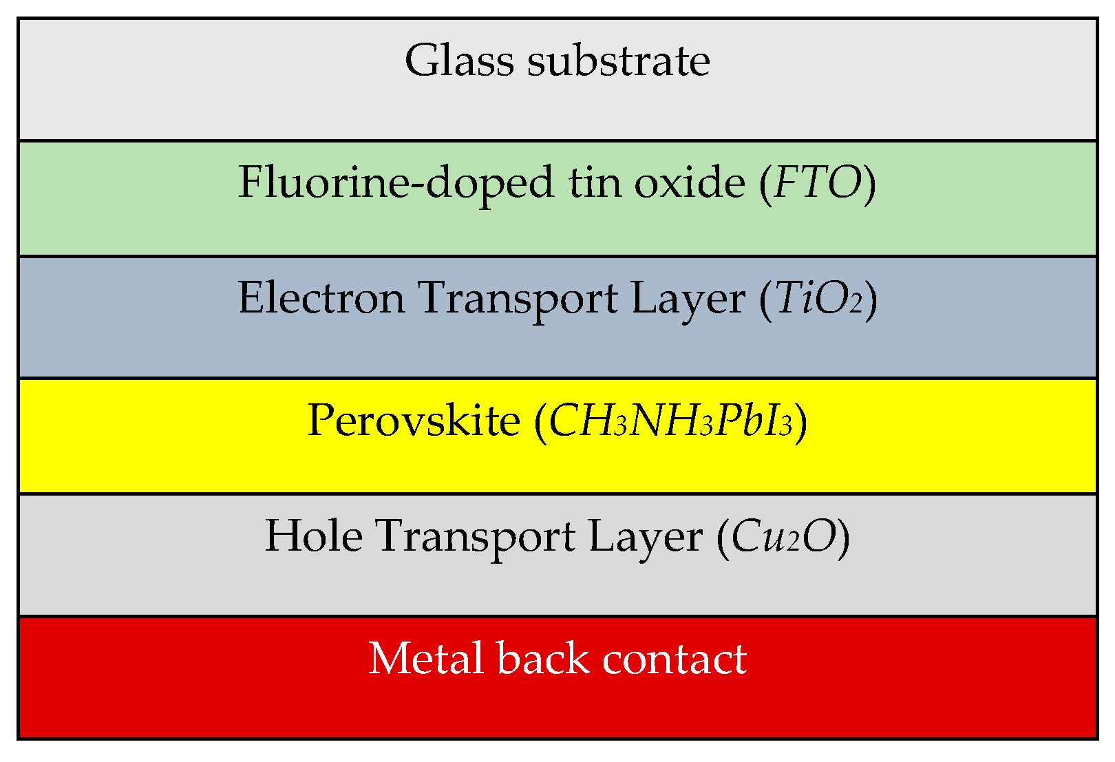
Figure 1. The basic structure of the perovskite solar.
Preprints 75736 g001
Figure 2. The J-V characteristics of the reference cell with Cu2O as HTM layer.
Preprints 75736 g002
Figure 3. Variation of defects density in absorber layer with Cu2O as HTM layer on PSC parameters: (a) PCE, (b) FF, (c) Jsc, (d) Voc.
Preprints 75736 g003
Figure 4. The change of cell performance: (a) PCE, (b) FF, (c) Jsc, (d) Voc versus the capture cross-section in the absorber layer with Cu2O as HTM layer.
Preprints 75736 g004
Figure 5. The vary of cell performance parameters (a) PCE, (b) FF, (c) Jsc, (d) Voc versus the defect’s density in the Cu2O/ absorber layer.
Preprints 75736 g005
Figure 6. Performance parameters (a) PCE, (b) FF, (c) Jsc, (d) Voc. versus defect density in the interface of absorber/ETM with Cu2O as HTM layer.
Preprints 75736 g006
Figure 7. Variation of defect density in absorber layer on cells performance normalized: (a) PCE, (b) FF, (c) Jsc, (d) Voc.
Preprints 75736 g007
Figure 8. Quantum efficiency of PSC with a variation of defect density in the absorber layer with Cu2O as HTM layer.
Preprints 75736 g008
Figure 9. The quantum efficiency of PSC with a variation of capture cross-section area in absorber layer with Cu2O as HTM layer.
Preprints 75736 g009
Figure 10. The correlation relationship between defects density and capture cross-section area in the absorber layer.
Preprints 75736 g010
Table 1. Simulation parameters of Perovskite solar cells devices [9,10,11,12].
Preprints 75736 i001
Table 2. The parameters of defects in the absorber and interface layers.
Preprints 75736 i002
Table 3. Capture electron and hole cross-sections of metal impurities in perovskite (CH3NH3PbI3) Solar cells.
Preprints 75736 i003
σn: capture cross-section of electrons. σp: capture cross-section of holes.
Disclaimer/Publisher’s Note: The statements, opinions and data contained in all publications are solely those of the individual author(s) and contributor(s) and not of MDPI and/or the editor(s). MDPI and/or the editor(s) disclaim responsibility for any injury to people or property resulting from any ideas, methods, instructions or products referred to in the content.
Copyright: This open access article is published under a Creative Commons CC BY 4.0 license, which permit the free download, distribution, and reuse, provided that the author and preprint are cited in any reuse.
Prerpints.org logo

Preprints.org is a free preprint server supported by MDPI in Basel, Switzerland.

Subscribe

© 2024 MDPI (Basel, Switzerland) unless otherwise stated