
Submitted:
30 May 2023
Posted:
31 May 2023
You are already at the latest version
Abstract
Miniature sensors are key components for the applications in the Internet of Things (IoT), wireless sensor networks, autonomous vehicles, smart cities and smart manufacturing. As a miniature and self-powered magnetic sensor, Wiegand sensor possesses the advantageous traits including changing-rate-independent output, low cost, and remarkable repeatability and reliability. Typical Wiegand sensor requires hard magnetic pole pieces that provide external fields for triggering voltage outputs that are called Wiegand pulses. However, the wire-shaped sensing element of Wiegand sensor is the critical issue that limits the design, selection, and adoption of the external triggering magnets. Currently, the widely used pole piece materials are rare-earth magnets. However, adopting rare-earth magnets brings strong stray fields, causing electromagnetic interference (EMI) problem. In this study, patterned CoNiP hard magnets were electrodeposited on flexible substrates through microfabrication. Origami magnetization was utilized to control the resultant stray fields, and hence the pole piece of CoNiP magnets can successfully trigger the output of Wiegand pulse. In comparison, the output voltage of the triggered pulse acquired through the patterned CoNiP magnets is comparable to that by using the rare-earth magnets. Furthermore, both the volume (meanwhile the weight) of the Wiegand sensor and the EMI issue can be significantly reduced and mitigated by the CoNiP magnets.
Keywords:
Wiegand sensor
; electrodeposited magnets
; microfabrication
; origami magnetization
; pole pieces
; trigging field
; Wiegand pulse
1. Introduction
Sensing technologies based on the magnetic properties of materials have drawn considerable interest due to the advantages of being non-contact and having a low input power requirement, superior energy efficiency, high sensitivity, and robust reliability against adverse environments [1,2]. Among the sensors that utilize various magnetic properties of materials, Wiegand sensors are found to be self-powered and stand alone for sensing and energy harvesting simultaneously [3,4,5]. Wiegand sensor is composed of a Wiegand wire that possesses different magnetic properties at the surface layer and the core, a pick-up coil that senses the change in magnetic flux of the Wiegand wire for inducing an output voltage pulse, and an external source of magnetic field to trigger the magnetic reversal of the Wiegand wire [6,7].
The pickup coil wound around the Wiegand wire is as shown in the Figure 1. Essentially, when the external magnetic field is applied in the opposite direction to the magnetization of wire, the magnetization of soft layer will flip first. During this process, there is a change in magnetic flux around the Wiegand wire. This change in the magnetic flux will induce an electromotive force in the pickup coil that can be visualized as a voltage pulse, also called as Wiegand pulse. Since the magnetization reversal of the soft layer in the Wiegand wire is rapid and steep, the magnetization jump in the Wiegand wire is usually called the large Barkhausen jump, and is also known as the Wiegand effect. The pulse generated by the Wiegand sensor will be used as a power supply for equipment without batteries.
The design and adoption of external triggering fields for the Wiegand sensor are limited by the wire-shaped sensing element of the Wiegand wire, which is a critical issue. Recently Lin et. al have thoroughly reviewed the distinctive Wiegand sensor and pointed out that the sophisticated design and fabrication of the triggering magnets are key to widen the application scenarios of Wiegand sensors [7]. Hard magnetic pole pieces that are capable to provide uniform external fields to trigger a uniform and complete magnetization reversal of the soft layer in the Wiegand wire are essential to maximize the output voltages. Currently, rare-earth magnets are widely used as pole piece materials, but they bring about strong stray fields that lead to electromagnetic interference (EMI) problems. Moreover, typical diameter of the Wiegand wire is 0.25 mm. Using bulk magnets impair the miniaturization capability of the Wiegand sensors. There is an urgent need to investigate the triggering magnets that are able to be compatible with microelectromechanical systems (MEMS) process for Wiegand sensor. In search of some facile materials, electrodeposited Co-rich alloys are potential candidates as hard magnetic pole pieces because they are high-throughput, high-energy-product permanent micro-magnets in a fully integrable and microfabrication-compatible manner.
Electrodeposited Co-rich magnets are promising candidates in MEMS applications such as actuators [8] in energy generation and harvesting systems [9], magnetic field sources in magnetic sensors [10], and magnetic scales in position measurement systems [11]. The utilisation of hard magnetic materials in MEMS application requires the consideration of cost-effective advantage over commonly used hard magnetic materials like sintered NdFeB. Various thin-film technologies, such as sputtering and molecular beam epitaxy, could be used to deposit thin magnetic films, like Co-based and rare earth alloys such as SmCo [12], with various magnetic anisotropy configurations. However, due to the limitation of these vacuum processes, only relatively thin layers can be produced, leading to weak magnetic field strength at working distances, which are typically not favored for their respective applications. The fabrication of thick magnetic layers could be realized using atomic layer deposition [13] technique due to agglomeration of powder magnets. But this process requires the use of rare earth elements to achieve sufficiently high magnetic fields at a given distance due to lower packing density. In search of alternative materials and deposition techniques, electrodeposited Co-based alloys [10] enables the cost-effective production of thick films and microfabrication manufactured micro-magnets with a high degree of geometric freedom and precision.
Co-based alloy films produced by electrodeposition, including CoP, CoPt, CoNiP, CoMnP, CoWP, CoPtP, and CoNiMnP, hold great promise for use in MEMS [14,15,16]. The magnetic properties of these alloys are significantly influenced by the Co content, grain size, and crystalline texture, which in turn affects the magnetocrystalline anisotropy (MA) [17] of the deposited films. Additionally, Co-rich alloys deposited by electrodeposition exhibit hard magnetic properties which result from the isolation of fine Co grains by the nonmagnetic elements that are segregated along grain boundaries [18]. For example, binary CoP alloy yields a high magnetic strength for a low P content and better process control, and the direction of MA can be tailored through the parameters of electrodeposition. Alloying significantly alters the MA of tertiary Co-rich alloys such as the in-plane (IP) type CoNiP alloy [11] and the out-of-plane (OP) type CoMnP alloy [19]. The enhancement of the magnetic flux can be realized through the increase in the thickness of the films without altering intrinsic magnetic properties such as MA, magnetization and energy product [20]. Moreover, Chen et.al., have demonstrated a strategy of multilayer engineering to preserve the OP magnetic properties while enhance the IP properties of the CoMnP alloy [21,22]. However, when a thick Co-based hard magnetic layer is microfabrication-patterned and magnetized, shape anisotropy can be the dominant effect depending on the specific geometry. Therefore, developing and improving a specialty magnetization process that yields a well-controlled profile of induction line at the working distances is challenging. In recent years, due to the rise of flexible material technology [23], magnetic materials have gradually developed towards curved surface magnetism (curvilinear magnetism), and correspondingly emerging magnetization techniques such as origami magnetization have found suitable for MEMS applications [24,25].
Flexible permanent magnets play a crucial role in the design of magnetically actuated micro-robots and microsystems that are manipulated through an external magnetic field [26,27]. Despite of being important in various applications, flexible permanent magnets pose a significant challenge in achieving optimal magnetic performance due to their ultrathin geometries [28]. In combination with the microfabrication patterning processes [10,15] and the origami techniques [24], the resultant enhanced magnetic field strength and well-controlled field profile allow for the effective utilization of thin, flexible permanent magnets, which in turn to be promising for the application in the Wiegand sensors. This prompted us to investigate the electrodeposited and origami magnetized Co-rich micro-magnets and evaluate the feasibility of being a triggering magnet for the Wiegand sensors.
The present study explores the potential of microfabrication processed CoNiP micro-magnets by electrodeposition on flexible substrates, which can be utilized to control the profile of stray field by means of origami magnetization. In-depth understanding of the effect of the triggering magnetic fields on the output pulse behaviour of a micro-scale Wiegand sensor is also studied. As a benchmark, we adopted a conventional NdFeB magnet to trigger Wiegand pulse and comparative results have been discussed.
2. Materials and Methods
2.1. Triggering Magnets and Material Characterization
In this research, typical compact-sized NdFeB magnet [Figure 2(a)] was utilized as a benchmark for comparing the triggered Wiegand pulses. Commercial flexible copper clad laminate (a.k.a. FCCL) are adopted as the flexible conductive substrates for the microfabrication of CoNiP micro-magnets. The consistency of the material properties of the FCCL substrates is excellent. The FCCL uses polyimide (PI) as its substrate and copper foil as the conductive layer, and the overall thickness is 50 μm.
Firstly, the as received FCCL substrate was cut into the size of 2.5 cm x 2.5 cm. The microfabrication of patterning and electrodeposition is based on an effective area defined by applying insulating Kapton tape to form a 2.0 cm x 2.0 cm area. The millimeter-scale pattern which defines the patterned areas to be electrodeposited was realized through sequentially applying Kapton tape and insulating varnish. The design of patterned micro-magnets is shown in Figure 2(b) with space (s) being 1.0 mm and width (w) of micro-magnet being 2.0 mm. After baking and curing, the Kapton tape was removed to form an insulating varnish pattern with a height of several hundred microns. After the electrodeposition process, the insulating varnish was removed using organic solvent (acetone). Finally, a pattern of electrodeposited Co-rich alloy was formed on FCCL substrate as shown in Figure 2(b).
Considering the need of uniform magnetic field profile in the horizontal (i.e., IP) direction, we adopted CoNiP alloy in the electrodeposition process. The formula of the electrodepositing bath is shown in Table 1. The electrodepositing process started with pre-treatment, including pickling for 20 seconds, water rinse, alkali wash for 5 seconds, water rinse, etc., followed by electrodepositing for 5 to 7 hours with the parameters shown in Table 1.
The fabricated sample was inspected with an optical microscope (OM), model Edge 3.0 AM73915MZT (Dino-Lite, Taiwan). A scanning electron microscope (SEM) was used to observe the surface morphology of the CoNiP film. The SEM model is HITACHI S-4800 (Japan). The SEM is equipped with an energy dispersive spectrometer (EDS) for qualitative and semi-quantitative composition analysis. In order to avoid the charge accumulation of high-energy electrons on the CoNiP surface, a nano-layer of platinum was evaporation deposited before observation. The working voltage of the SEM was 4~10kV. X-ray diffractometer (XRD) was used to analyze the crystal structure of the CoNiP film. The XRD is the TTRAX Ⅲ type XRD produced by Rigaku (Japan) equipped with the light source of Cu Kα . The operating voltage was 15kV.
A superconducting quantum interference device magnetometer (SQUID) was used to measure the magnetic properties of the CoNiP sample for obtaining the hysteresis curves. The instrument is produced by Quantum Design in the United States, and the model is MPMS-3. The instrument can apply the external field in the range of ±70,000 Gauss (G) at the temperature between 1.9~400 K, and the measurable magnetization range is from 5×10⁻⁸ emu to 300 emu. In the measurement, the normal (i.e., OP) direction of the CoNiP coating and the horizontal (i.e., IP) direction of the CoNiP coating were characterized.
2.2. Origami Magnetization and the Measurement of Magnetic Field Profile
A C-shaped magnetizing head (Figure 3(a)) is designed to generate a uniformly applied magnetic field of 1.5 T for magnetization. Three configurations of magnetization including flat, curved, and annular CoNiP samples were realized through 3D-printed sample holders. The details of the 3D-printed sample holder for the curved magnetization are depicted in the Figure 3(b). The directions of the origami curling and the applied field are indicated as shown in Figure 2(b). During the curved magnetization process, the sample holder allowed the CoNiP sample being clamped in the U-shaped groove of two holding fixtures. For annular magnetization, another 3D-printed sample holder as shown in Figure 3(c) was employed. Capacitive discharge pulse magnetizer (Ney Hwu Electrical Co., Ltd., Taiwan) was used as the excitation source for magnetization with a current setting of 500 A.
Figure 4 illustrates the apparatus and method for measuring the stray field profile of the hard magnets. The hard magnets were positioned on the moving platform composed of a servo-controlled stepper motor (08PTM-50M, Unice E-O Services Inc., Taiwan), which has a minimum step size of 2.5 μm and a repeatability of 5 μm. A Hall sensor tip of a Gaussmeter (F.W. Bell 5180, USA) was then fastened on a manual stage that provides fine adjustment in y- and z-axis directions and θ rotation. The sensing directions of the Hall sensor includes two IP directions and one OP direction (Figure 2(b)). The direction aligned to the Hall sensor moving (relatively to the platform) direction was defined as the IP-X direction. The same method of defining directions applied to the NdFeB magnet (Figure 4). Both the long-side and short-side of the NdFeB magnet were measured as depicted in Figure 2(a). In the measurement process, firstly the Hall sensor sensing direction was adjusted and aligned with the principal direction of stray field so that the reading value of the Gaussmeter reached the local maximum. Next, the Hall sensor height in the z-axis was adjusted to search for a flight height providing with a magnetic field strength of about 100 G. The minimum flight height of the Hall sensor was 0.5 mm if there was no 100 G field strength. Finally, the platform of the motorized linear stage was controlled to translate the hard magnet at an increment of 0.1 mm each step. Then the field strength of each step and therefore the profile of stray field can be measured at a specific flight height above the patterned CoNiP magnet or NdFeB magnet.
2.3. Output Voltage Measurement of the Triggered Wiegand Pulses
The experimental setup includes a DAQ (USB-6210, National Instruments (NI), USA), Labview program and a manual linear guide slide platform in order to measure the Wiegand out pulse (Figure 5). The Wiegand wire used in this experiment was taken from commercially available Wiegand sensor, WG631. And its specifications are detailed in Table 2 [29]. We extracted the Wiegand wire and made a custom Wiegand sensor using a sectioned Wiegand wire in a length of 9.0 mm with a pick-up coil of 121-turn winding.
The Wiegand sensor is fixed in a clampable customized jig, and the entire jig is placed on an adjustable track to facilitate the adjustment and fixation of flight height. Note that the patterned CoNiP hard magnet was flattened when in use to trigger the Wiegand sensor. The relative motion between hard magnets and the Wiegand sensor was realized through a manual linear guide slide. To ensure a same initial status of Wiegand wire magnetization, it is necessary to flip the magnetic polarity of the Wiegand wire into an identical polarization using a magnet before triggering the Wiegand pulse. In the current study, positive pulses were generated, recorded and compared. The flight height between the hard magnets and the Wiegand sensor was adjusted step-wisely (e.g., ±0.5 mm per step), and the aforementioned Wiegand pulse measurement was repeated in order to find the optimal output voltage of the Wiegand pulse. As a benchmark, a commercially available NdFeB magnet was employed to trigger the Wiegand output pulse through the same method, and the results were compared and discussed.
3. Results and Discussion
3.1. NdFeB Magnets and Output Pulses
Figure 6 shows the measurement results of the spatial distribution of stray field intensity on the NdFeB magnet for triggering the Wiegand pulse. It is evident that the long-side has distinguishable IP-X and IP-Y magnetic field strengths, while the short-side has a similar IP-X and IP-Y magnetic field strength forming an equi-biaxial magnetic field in the IP directions.
Figure 7 depicts the output voltage of Wiegand pulse triggered at different flight height using the NdFeB magnet. The background noise is approximately in a range of 0.0005 V. In the case of NdFeB magnet, it is evident from Figure 7(a,b) that the long-side triggering method yields a maximum output pulse of 0.023 V at a flight height of 25 mm, while the short-side triggering method produces a maximum output pulse of 0.014 V at a flight height of 20 mm. Such an output voltage difference is because when the short-side of NdFeB is used for triggering pulses, the Wiegand wire experiences multi-directional triggering field in the plane (that is, the plane formed by the moving Wiegand wire at a fixed flight height) where the magnetic field strengths in the IP-X and IP-Y directions are similar (Figure 6(b)). The influence of the equi-biaxial magnetic field leads to a disturbance to the magnetic reversal [30], making the overall output pulse voltage lower.
3.2. Microfabrication and Origami Magnetization of CoNiP Micro-magnets
The magnetic studies of the CoNiP coating performed using SQUID suggest that the hard magnetic properties in the IP direction are better than those in the OP direction (Figure 8(a)). As shown in Table 3, there is little difference in the coercive force (Hc) along the horizontal direction and the vertical direction. The coercive force is recorded as about 1100 Oe in both directions. On the other hand, there is a significant variation in the residual magnetization (Br). The residual magnetization in the IP direction is 4200 G, which is much higher than the residual magnetization in the OP direction, measuring 2500 G only. This remarkable difference in the residual magnetic flux density is ascribed to the magnetocrystalline anisotropy as well as shape anisotropy of the coating.
To study the crystal structure of the CoNiP coating, XRD technique was employed and the recorded XRD pattern is shown in Figure 8(b). The first peak in the XRD pattern is identified as Co HCP (100), indicating that the horizontal MA which leads to better magnetic properties in the horizontal direction of the CoNiP coating. The evidenced low intensity of HCP (002) compared to that of HCP (100) indicates that the CoNiP coating has a significant preferred orientation of HCP c-axis aligned in the horizontal direction. SEM results indicate that the CoNiP coating possesses nano-sized grain. And the EDS results illustrate that the cobalt content is 87.1 ± 2.8 wt.%, the nickel content is 10.2 ± 0.6 wt.%, and the phosphorus content is 2.7 ± 0.2 wt.%, representing a Co-rich coating.
Figure 9(a) shows the photos of the patterned CoNiP magnet manufactured through the microfabrication process. The designed pattern can be completely formed, resulting in a flexible hard magnetic component. By inspecting the millimetre-scale pattern as depicted in Figure 9(b), it is clear to see that a desired pattern of thick CoNiP coating was able to be realized through the microfabrication process using insulating varnish patterns.
The CoNiP sample was magnetized using the C-shaped magnetizing head by keeping the strip range against one open end of the C-shaped head. Once magnetization process was completed, we performed quick measurements for the IP-X magnetic field strength using the Gaussmeter at nine positions above the CoNiP sample as shown in Figure 10(a). After such preliminary and screening measurements, the spatial distribution of stray field strength of the CoNiP samples were measured. As illustrated in Figure 10(b) through 10(d), in the whole 2 cm × 2 cm patterned CoNiP samples the upper part (regions i, ii, iii) represent S polarity, while the lower part (regions vii, viii, ix) represent N polarity. The highest magnetic field strength obtained on each sample falls in the upper part of the sample, which is also the strip region used to trigger the Wiegand pulse. For the strip regions, the maximum magnetic field strength of the flat magnetized sample is about -60 G, and the minimum one is -0.2 G as shown in Figure 10(b). This result indicates that the difference in magnetic field strength caused by fringe effect can reach hundreds of times. On the other hand, the maximum magnetic field strength of the curved CoNiP sample by origami magnetization is about -100 G, and the minimum one is about -50 G. The difference in magnetic field strength caused by the fringe effect drops to about 2 times, as depicted in Figure 10(c). This difference can be further reduced to less than 2 times by annular origami magnetization, as shown in the Figure 10(d).
3.3. CoNiP Micro-magnets and Output Pulses
Figure 11 depicts the outcomes of the spatial distribution of stray field intensity measured form the CoNiP samples used to trigger Wiegand pulses in this study. Note that the flat magnetized CoNiP sample can hardly trigger any Wiegand pulses. It is clear to see that the field strength in two IP directions (i.e., IP-X and IP-Y) has significant difference, and the OP field strength is much weaker comparing with any of the IP field strength. Note that the flight height of the Hall sensor probe tip of the Gaussmeter is 0.5 mm when characterizing the CoNiP samples. The Wiegand pulse triggering experiment was carried out using the regions as indicated by the red-dashed arrows in the Figure 11 (at a flight height around 0.5 mm). On comparing the results of the patterned CoNiP and the commercial NdFeB magnets, one can conclude that a single-axis stray field in the plane where Wiegand wire flies is achieved through the formation of magnetocrystalline anisotropy and shape anisotropy of the patterned CoNiP magnet. It is also found that origami magnetization can effectively control the magnetic field strength and profile, which is difficult to tackle for bulk and rigid magnets due to fringe effect.
Figure 12(a) represents the result of Wiegand pulse triggering test conducted using the strip region of the patterned CoNiP magnet, and it reveals that the maximum pulse voltage of about 0.027 V is achieved at a flight height of 0.5 mm. Note that the output pulse voltage decreases when the flight height deviates from the optimal ones [6]. The above results suggest that the external magnetic field having a prominently uniaxial stray field is key to maximize the output voltage when the principal axis of stray field aligns well with the Wiegand wire. In this way, the three-dimensional tensor of the stray field distribution can exactly fit for the wire-shaped Wiegand element (as illustrated in Figure 11) to gigantically trigger the magnetization reversal.
The results of the optimal output pulses are summarized in Figure 12(b) for the comparison between the patterned CoNiP micro-magnet and the NdFeB magnet. The peak voltage values of the optimal pulses triggered by the patterned CoNiP and the long-side of NdFeB magnets are similar (both around 0.025 V). On the other hand, the annular magnetized CoNiP magnet produces a peak voltage value of 0.018 V, and the NdFeB short-side triggered output pulse is 0.014 V. Besides, all measurement results indicate that the full width at half maximum (FWHM) of all the triggered pulses is in the range of 10 μs to 30 μs, which is consistent with the specification as show in Table 2, representing a typical Wiegand pulse.
4. Conclusions
In this study, electrodeposited CoNiP hard magnets on flexible substrates were successfully patterned using microfabrication technique. The patterned CoNiP magnets can be origami magnetized to realize an engineered stray field. This study has illustrated the effectively triggering Wiegand pulses using the pole piece of CoNiP micro-magnets. The results of the study indicate that the output voltage of the triggered pulse using the patterned CoNiP magnets is comparable to that acquired using rare-earth magnets. Additionally, the use of CoNiP micro-magnets allows for a significant reduction in both the volume of the Wiegand sensors and the EMI issue.
In the future the MEMS-process-compatible electrodeposited Co-rich micro-magnets can help and facilitate the application designs of Wiegand sensors. The positive and negative Wiegand pulses can be modulated directly through the specialty patterned and magnetized micro-magnets. Further parameters of Wiegand sensors including the hard layer polarization, length of Wiegand wire (i.e., the ratio of wire length to wire radius) and the shape (through the alternative materials that can realize Wiegand effect) can be efficiently utilized because of the breakthrough of the controlled magnetic field profile of the triggering magnets. Novel Wiegand-sensor-integrated devices such as self-powered positioning systems and rectifier-free energy harvester will be possible to realize through further research and development.
Author Contributions
Conceptualization, C.-C.L.; methodology, G.K., Y.C. and C.-C.L.; software, Y.C.; validation, G.K.; formal analysis, Y.C. and C.-C.L.; investigation, G.K.; resources, C.-C.L.; data curation, Y.C.; writing—original draft preparation, G.K. and C.-C.L.; writing—review and editing, G.K. and C.-C.L.; visualization, G.K. and C.-C.L.; supervision, C.-C.L.; project administration, C.-C.L.; funding acquisition, G.K. and C.-C.L. All authors have read and agreed to the published version of the manuscript.
Funding
This research was funded by the National Science and Technology Council (NSTC), Taiwan, grant number 110-2221-E-035-047 and 111-2221-E-035-051. The authors are grateful to VIT-AP University for the financial support through RGEMS, grant number VIT-AP/SPORIC/RGEMS/2022-23/011.
Data Availability Statement
All data that support the findings of this study are included within the article.
Acknowledgments
The authors would like to extend their appreciation to Prof. J.-Y. Chang at National Tsing Hua University for his kind technical supports on the measurement of Wiegand pulse.
Conflicts of Interest
The authors declare no conflict of interest. The funders had no role in the design of the study; in the collection, analyses, or interpretation of data; in the writing of the manuscript; or in the decision to publish the results.
References
- Mohammed, A.K.; Jian, S.; Bodong, Li.; Alexander, P.; Jürgen, K. Magnetic sensors-A review and recent technologies. Eng. Res. Express 2021, 3, 022005. [Google Scholar] [CrossRef]
- Pallás-Areny, R.; Webster, J.G. Sensors and Signal Conditioning, 2nd ed.; John Wiley & Sons: Hoboken, NJ, USA, 2001; 254–256. [https://books.google.com/books?hl=en&lr=&id=BDmQDQAAQBAJ&oi=fnd&pg=PR3&ots=z8apbWKnPS&sig=KdtYatucNSfIuLgLjPbg6GCm4yk]. [Google Scholar]
- Wiegand, J.R.; Multiple Pulse Magnetic Memory Units. U.S. Patent 3,602,906, 31 August 1971 [https://scholar.google.com/scholar_lookup?title=Multiple+Pulse+Magnetic+Memory+Units&author=Wiegand,+J.R.&publication_year=1971].
- Wiegand, J.R.; Bistable Magnetic Device. U.S. Patent 3,820,090, 25 June 1974 [https://scholar.google.com/scholar_lookup?title=Bistable+Magnetic+Device&author=Wiegand,+J.R.&publication_year=1974].
- Wiegand, J.R.; Method of Manufacturing Bistable Magnetic Device. U.S. Patent 3,892,118, 1 July 1975 [https://scholar.google.com/scholar_lookup?title=Method+of+Manufacturing+Bistable+Magnetic+Device&author=Wiegand,+J.R.&publication_year=1975].
- Yang, C.; Sakai, T.; Yamada, T.; Song, Z.; Takemura, Y. Improvement of pulse voltage generated by Wiegand sensor through magnetic-flux guidance. Sensors 2020, 20, 1408. [Google Scholar] [CrossRef] [PubMed]
- Lin, C.-C.; Tseng, Y.-C.; Chin, T.-S. A review of the self-powered Wiegand sensor and its applications. Magnetochemistry 2022, 8, 128. [Google Scholar] [CrossRef]
- Liakopoulos, T.M.; Zhang, W.; Ahn, C.H. Electroplated Thick CoNiMnP Permanent Magnet Arrays for Micromachined Magnetic Device Applications. Proceeding IEEE MEMS’ 96, 1996, 79–84. [Google Scholar] [CrossRef]
- Han, M.; Yuan, Q.; Sun, X. Design and fabrication of integrated magnetic MEMS energy harvester for low frequency applications. J. Microelectromech. Syst. 2014, 23, 204–212. [Google Scholar] [CrossRef]
- Myung, N.V.; Park, D.Y.; Yoo, B.Y.; Sumodjo, P.T.A. Development of electroplated magnetic materials for MEMS. J Magn Magn Mater 2003, 265, 189–198. [Google Scholar] [CrossRef]
- Xu, Z.-H.; Tseng, B.-H.; Ching, C.; Wang, S.-C.; Chin, T.-S.; Sung, C.-K. Grooved multi-pole magnetic gratings for high-resolution positioning systems. Jpn. J. Appl. Phys. 2015, 54, 06FP01. [Google Scholar] [CrossRef]
- Sharma, S.; Radulov, I.; Major, M.; Alff, L. Evolution of magnetic anisotropy with Sm contents in Sm–Co thin films. IEEE Trans. Magn. 2018, 54, 1–5. [Google Scholar] [CrossRef]
- Reimer, T.; Lofink, F.; Lisec, T.; Thede, C.; Chemnitz, S.; Wagner, B. Temperature-stable NdFeB micromagnets with high-energy density compatible with CMOS back end of line technology. MRS Advances, 2016, 1, 209–213. [Google Scholar] [CrossRef]
- Sun, X.; Yuan, Q.; Fang, D.; Zhang, H. Electrodeposition and characterization of CoNiMnP permanent magnet arrays for MEMS sensors and actuators. Sens. Actuators A 2012, 188, 190–197. [Google Scholar] [CrossRef]
- Li, Y.; Kim, J.; Kim, M.; Armutlulu, A.; Allen, M.G. Thick multilayered micromachined permanent magnets with preserved magnetic properties. J. Microelectromech. Syst. 2016, 25, 498–507. [Google Scholar] [CrossRef]
- Siang, J.; Lim, M.H.; Leong, M.S. Review of vibration-based energy harvesting technology: mechanism and architectural approach. Int. J. Energy Res. 2018, 42, 1866–93. [Google Scholar] [CrossRef]
- Qiao, G.Y.; Xiao, F.R. Effects of grain size on the properties of bulk nanocrystalline Co-Ni alloys. Mater. Res. Express 2017, 4, 086512. [Google Scholar] [CrossRef]
- Lu, N.; Li, Y.; Cai, J.; Li, L. Synthesis and characterization of ultrasonic-assisted electroplated Co-P films with amorphous and nanocrystalline structures. IEEE Trans. Magn. 2011, 47, 3799–802. [Google Scholar] [CrossRef]
- Wu, C.-W.; Lin, C.-C.; Chin, T.-S.; Chang, J.-Y.; Sung, C.-K. Effects of cathode rotation and substrate materials on electrodeposited CoMnP thick films. Mater.Res. Express 2020, 8, 016103. [Google Scholar] [CrossRef]
- Wang, Z.K.; Feng, E.X.; Liu, Q.F.; Wang, J.B.; Xue, D.S. Tuning stress-induced magnetic anisotropy and high frequency properties of FeCo films deposited on different curvature substrates. Phys. B: Condens. Matter. 2012, 407, 3872–3875. [Google Scholar] [CrossRef]
- Chen, Y.-S.; Lin, C.-C.; Chin, T.-S.; Chang, J.-Y.; Sung, C.-K. Residual stress tuned magnetic properties of thick CoMnP/Cu multilayers. AIP Adv. 2022, 12, 035022. [Google Scholar] [CrossRef]
- Chen, Y.-S.; Lin, C.-C.; Chin, T.-S.; Chang, J.-Y.; Sung, C.-K. Residual stress analysis of electrodeposited thick CoMnP monolayers and CoMnP/Cu multilayers. Surf. Coat. Technol. 2022, 434, 128169. [Google Scholar] [CrossRef]
- Felix, G.; Dmitriy, D.K.; Daniil, K.; Oliver, G.S. Magnetic origami creates high performance micro devices. Nat. Commun. 2019, 10, 3013. [Google Scholar] [CrossRef]
- Ya, L.; Zhijie, Q.; Jingxuan, Y.; Mingxing, Z.; Xin, Z.; Wei, L.; Yingying, Z.; Ziyue, W.; Hanjie, W.; Baoan, N.; Hang, X.; Wenxing, H.; Xian, H. Origami NdFeB flexible magnetic membranes with enhanced magnetism and programmable sequences of polarities. Adv. Funct. Mater. 2019, 29, 1904977. [Google Scholar] [CrossRef]
- Ze, Q.; Wu, S.; Nishikawa, J.; Dai, J.; Sun, Y.; Leanza, S.; Zemelka, C.; Novelino, L.S.; Paulino, G.H.; Zhao, R.R. Soft robotic origami crawler, Sci. Adv. 2022, 8, eabm7834. [Google Scholar] [CrossRef]
- Hu, W.; Lum, G.-Z.; Massimo, M.; Metin, S. Small-scale soft-bodied robot with multimodal locomotion. Nature 2018, 554, 81. [Google Scholar] [CrossRef] [PubMed]
- Xu, T.; Zhang, J.; Mohammad, S.; Onaizah, O.; Eric, D. Millimeter-scale flexible robots with programmable three-dimensional magnetization and motions. Sci. Rob. 2019, 4, eaav4494. [Google Scholar] [CrossRef] [PubMed]
- Aleksandra, R.; Zbigniew, J. G.; Waldemar, K. On the air enrichment by polymer magnetic membranes. J. Membr. Sci. 2009, 336, 79. [Google Scholar] [CrossRef]
- http://www.ahest.com/.
- Lien, H.-L.; Chang, J.-Y. Magnetic reference mark in a linear positioning system generated by a single Wiegand pulse. Sensors 2022, 22, 3185. [Google Scholar] [CrossRef]
Figure 1.
Schematic representation of the Wiegand effect.
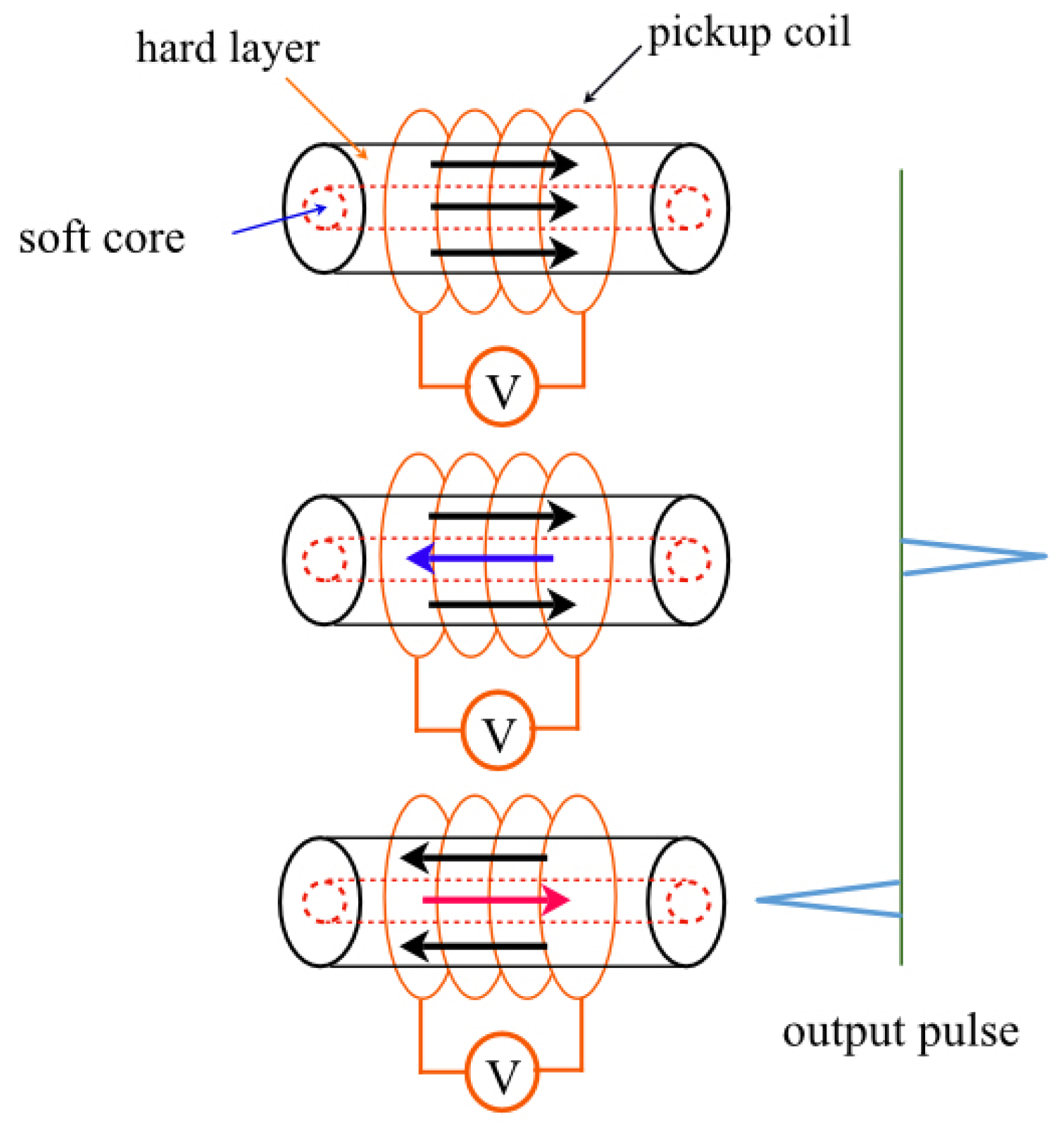
Figure 2.
(a) The NdFeB magnet, and (b) schematic drawing of the patterned CoNiP magnet, showing the geometries and the definitions of the measurement directions for the magnets. The blue arrows illustrate the Hall sensor sensing directions (out-of-plane (OP) being normal to in-plane (IP) directions), while the red-dot arrows indicate the moving tracks of the Hall sensor tip. In (b), the directions of applied field for magnetization (black arrow) and sample curling for origami (green arrows) are illustrated accordingly.
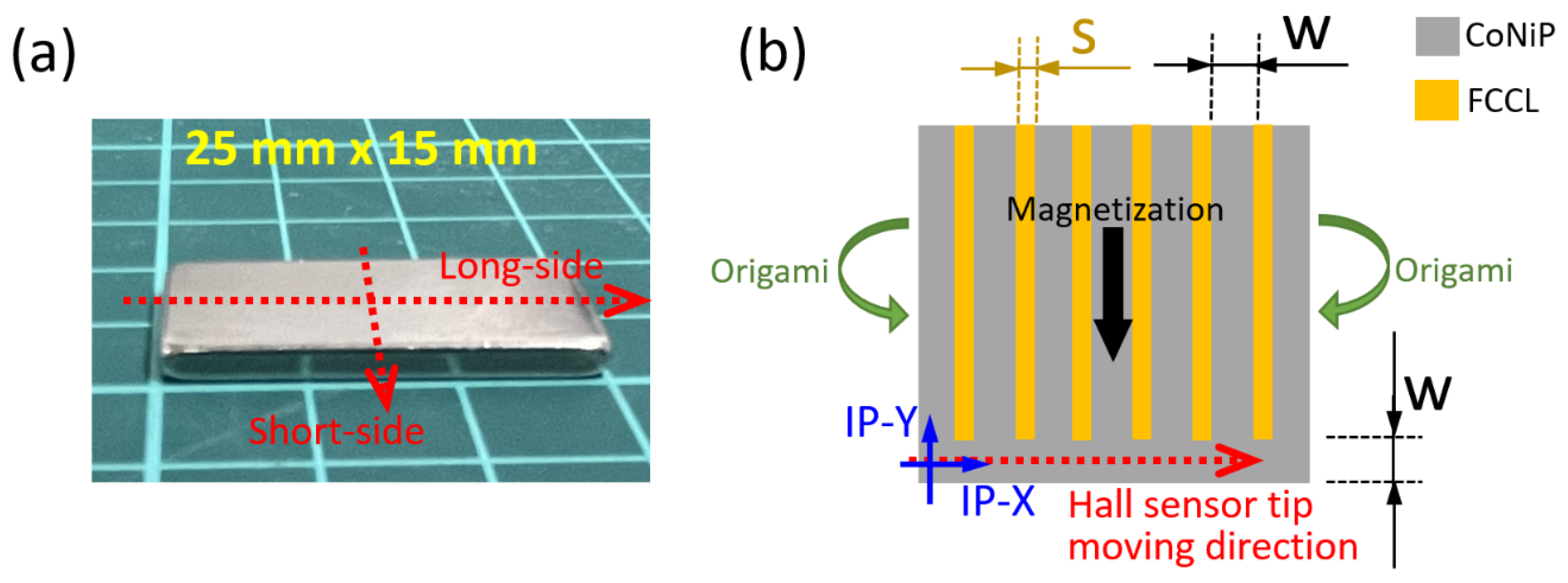
Figure 3.
Details of the magnetization setups: (a) the C-shaped magnetizing head and the 3D-printed sample holder; (b) 3D CAD model of the sample holder and its exploded-view; (c) sample holder along with a patterned CoNiP sample for annular magnetization.
Figure 3.
Details of the magnetization setups: (a) the C-shaped magnetizing head and the 3D-printed sample holder; (b) 3D CAD model of the sample holder and its exploded-view; (c) sample holder along with a patterned CoNiP sample for annular magnetization.
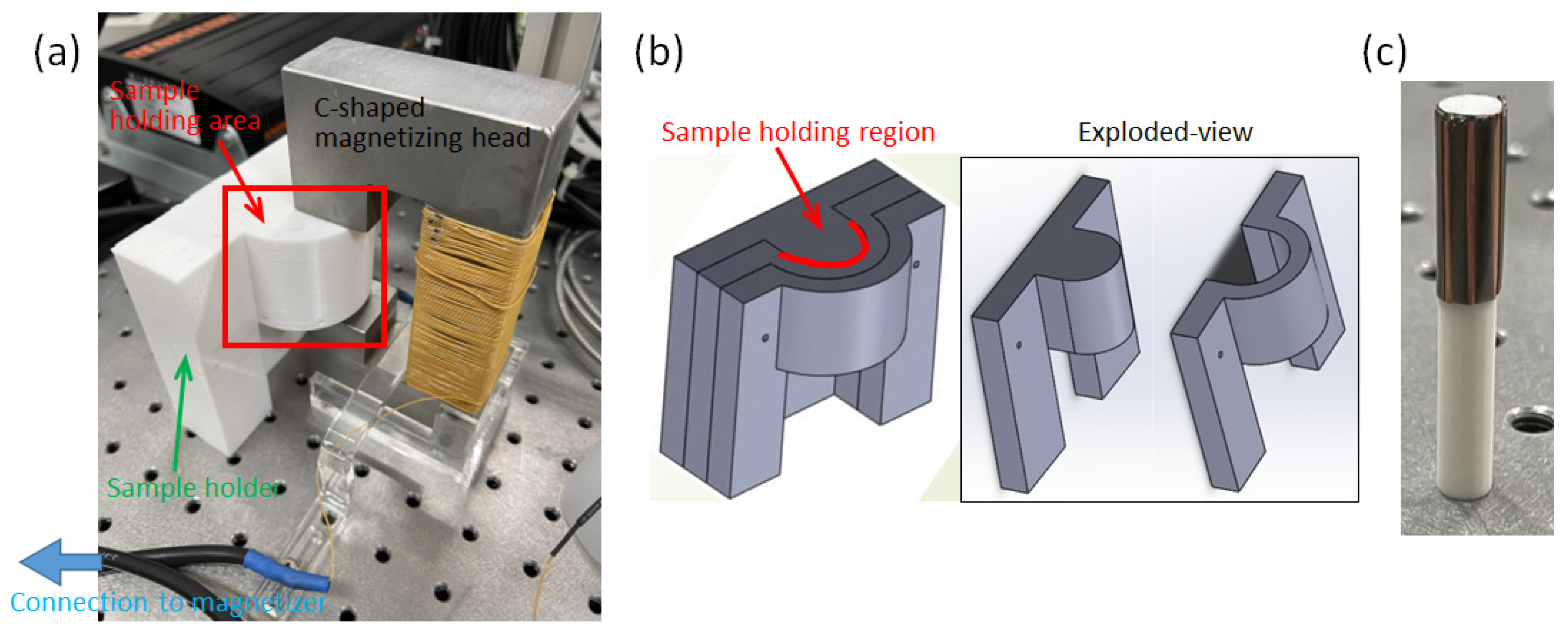
Figure 4.
Apparatus composed of a Hall sensor, a y-z-θ manual stage and a motorized linear stage for measuring the magnetic flux density profile of the magnets.
Figure 4.
Apparatus composed of a Hall sensor, a y-z-θ manual stage and a motorized linear stage for measuring the magnetic flux density profile of the magnets.
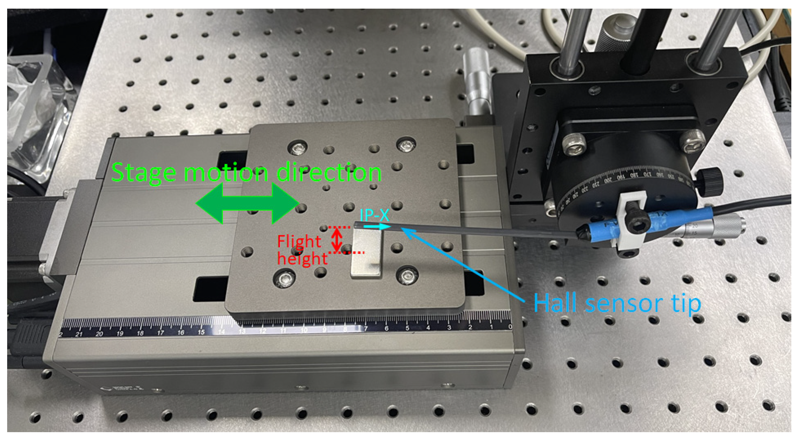
Figure 5.
Schematic drawing showing the setup for Wiegand pulse measurement.
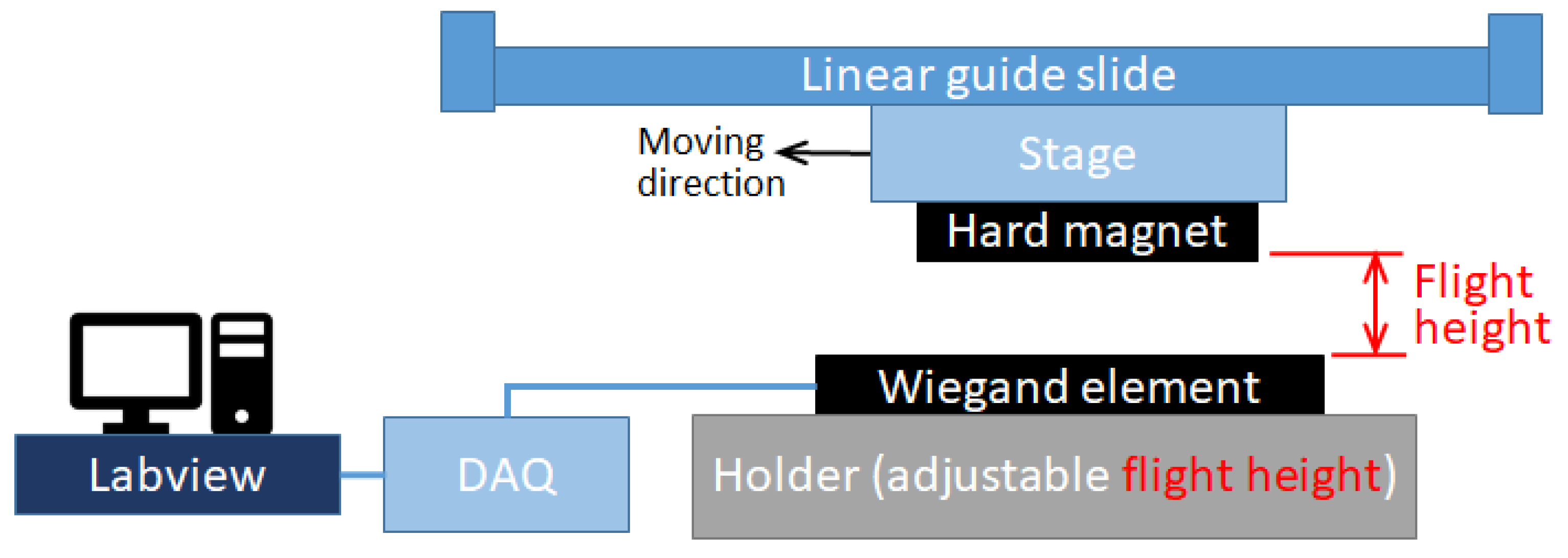
Figure 6.
Measurement results of the magnetic flux density profiles of the NdFeB magnets along (a) the long-side, and (b) the short-side.
Figure 6.
Measurement results of the magnetic flux density profiles of the NdFeB magnets along (a) the long-side, and (b) the short-side.
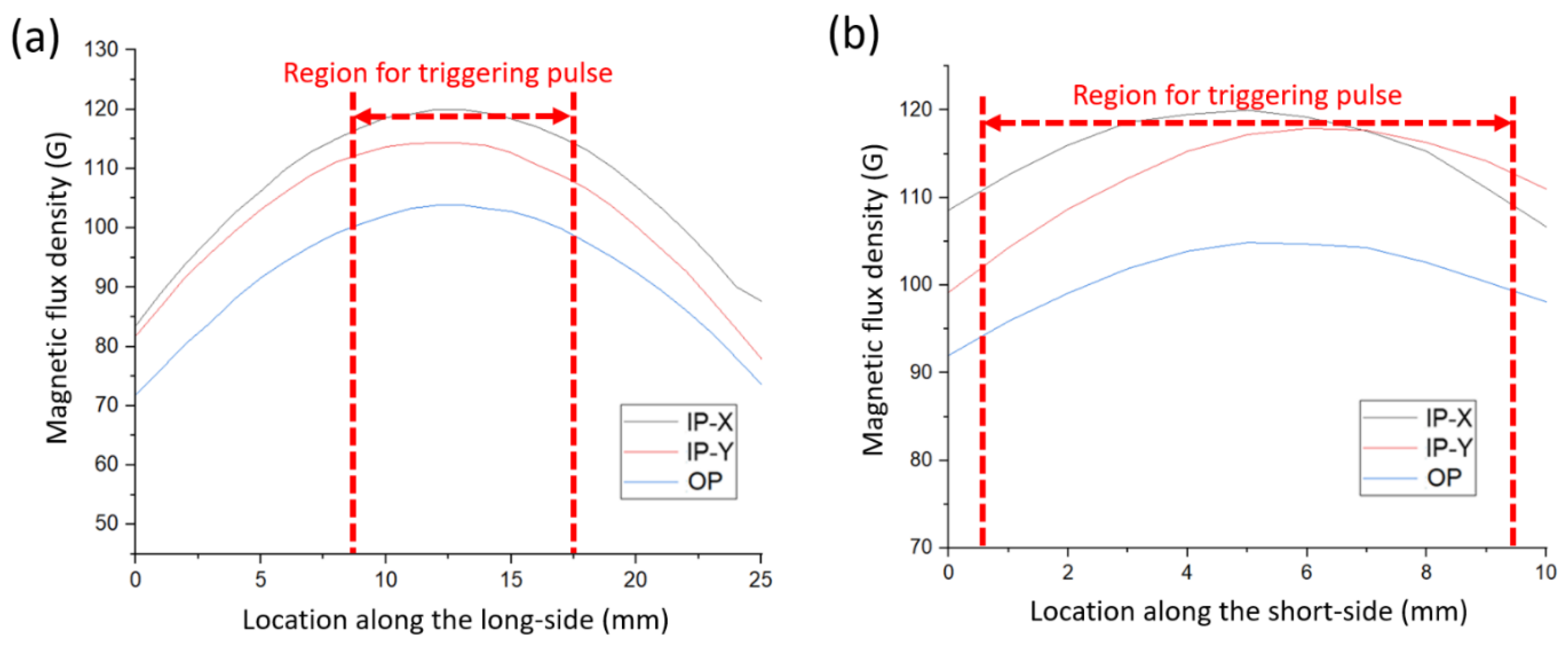
Figure 7.
Output pulses (presented in stacked format) as a function of flight height: (a) triggered using the long-side of NdFeB magnet, (b) triggered using the short-side of NdFeB magnet.
Figure 7.
Output pulses (presented in stacked format) as a function of flight height: (a) triggered using the long-side of NdFeB magnet, (b) triggered using the short-side of NdFeB magnet.
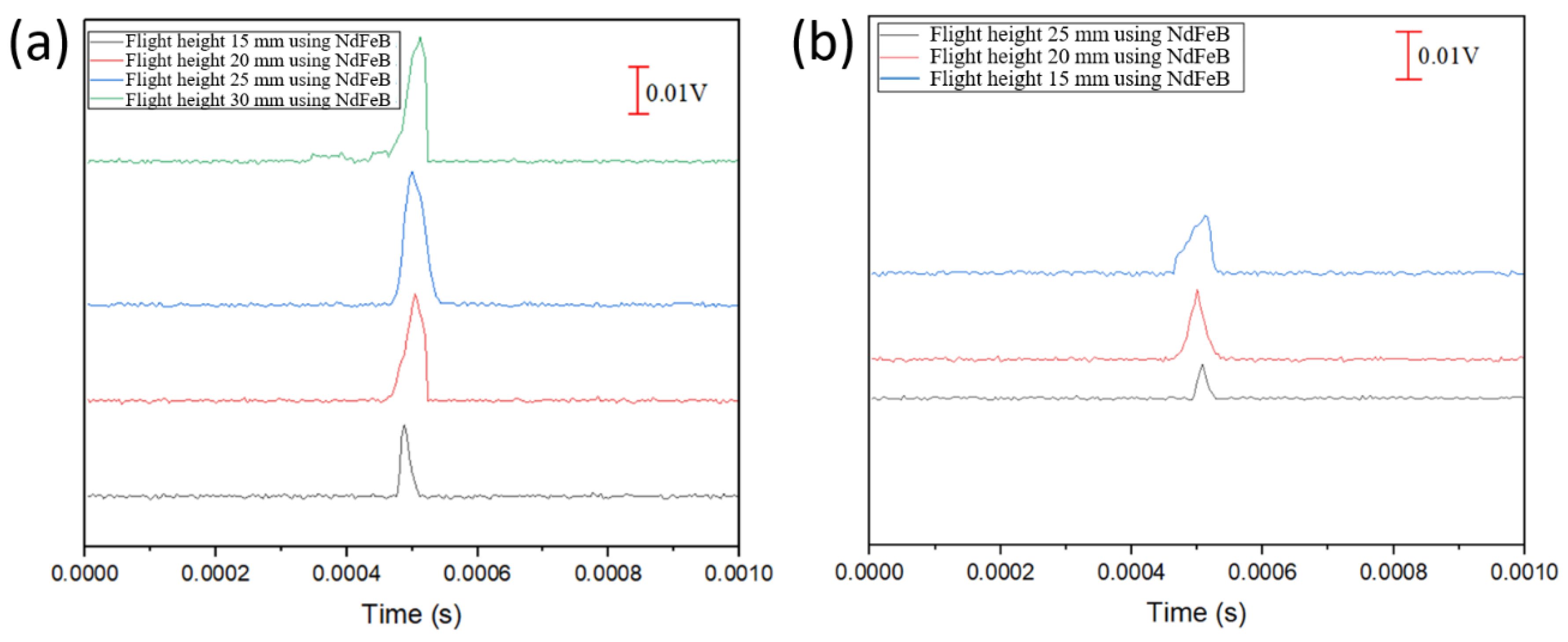
Figure 8.
Materials characterization results of CoNiP magnets showing (a) the SQUID acquired second quadrant of B-H curve, and (b) the XRD pattern along with the information of JCPDS (Joint Committee on Powder Diffraction Standards) cards for cobalt.
Figure 8.
Materials characterization results of CoNiP magnets showing (a) the SQUID acquired second quadrant of B-H curve, and (b) the XRD pattern along with the information of JCPDS (Joint Committee on Powder Diffraction Standards) cards for cobalt.
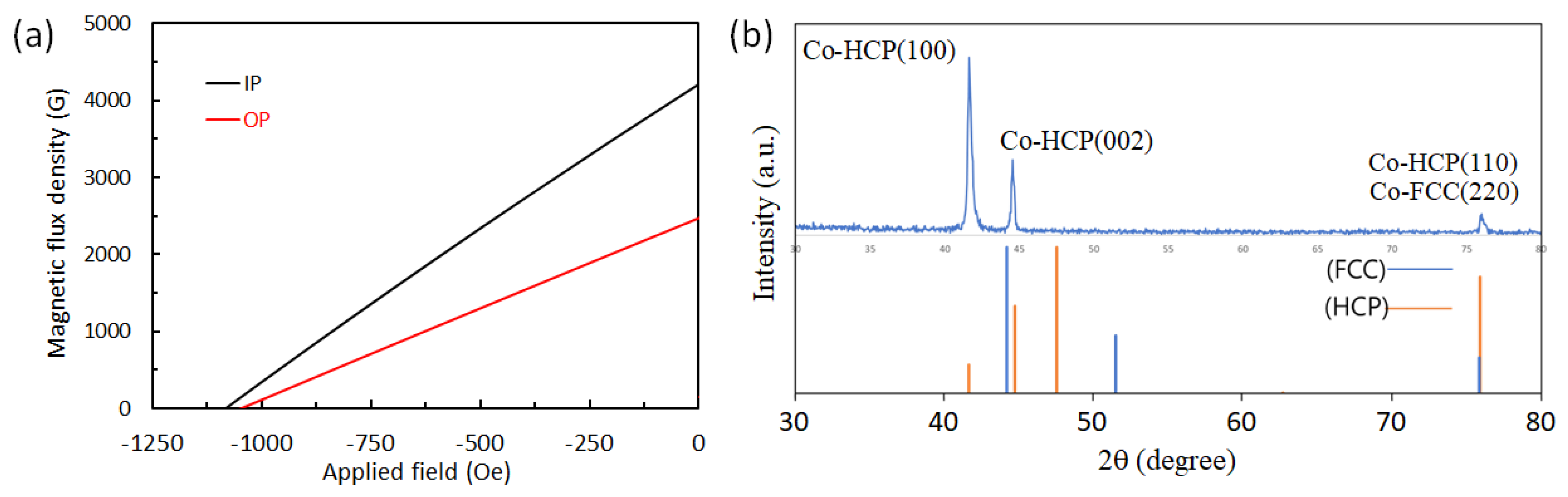
Figure 9.
(a) Photo of the patterned CoNiP magnet; and (b) the zoom-in image of the red-rectangular area in (a).
Figure 9.
(a) Photo of the patterned CoNiP magnet; and (b) the zoom-in image of the red-rectangular area in (a).
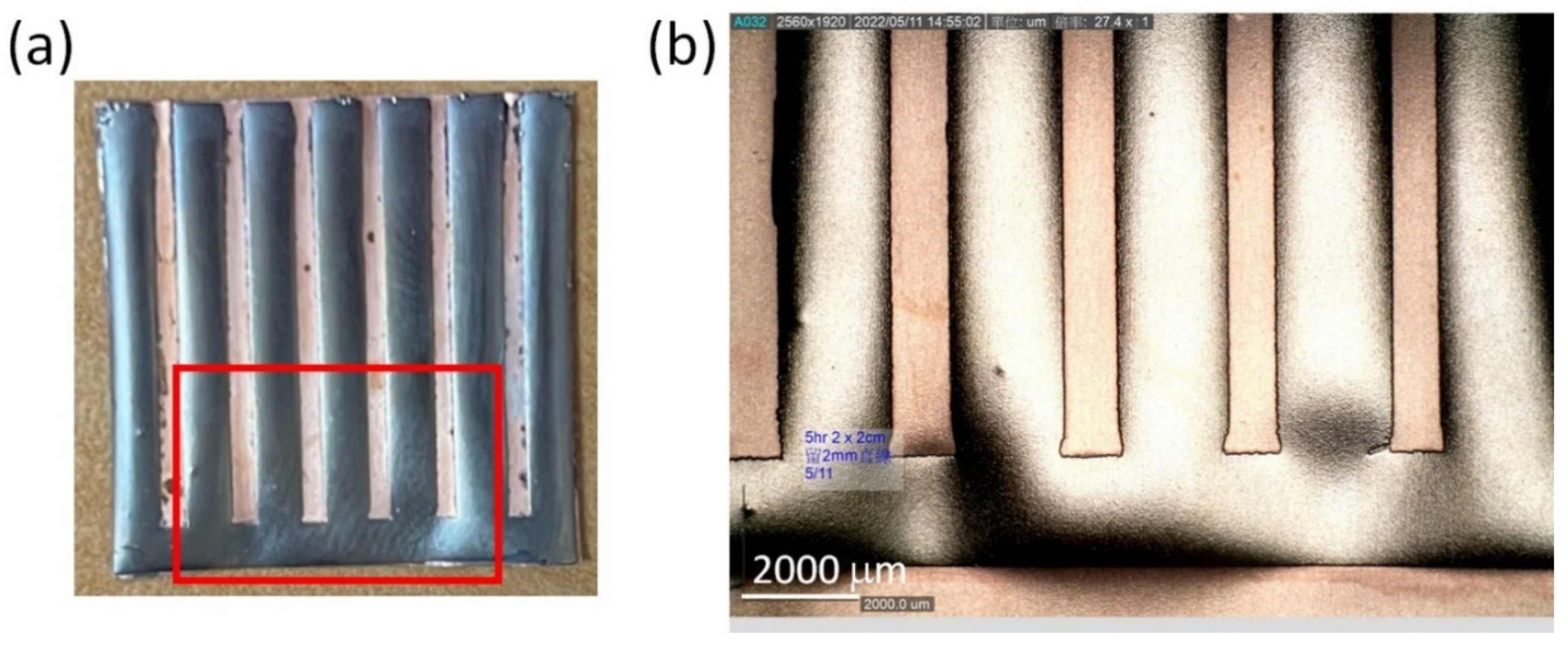
Figure 10.
Brief measurement of the stray field intensities above the patterned CoNiP magnets: (a) definition of the nine (9) measurement locations; and the stray field intensities (unit in Gauss) in the nine locations of the CoNiP magnets after (b) flat magnetization, (c) curved magnetization, and (d) annular magnetization.
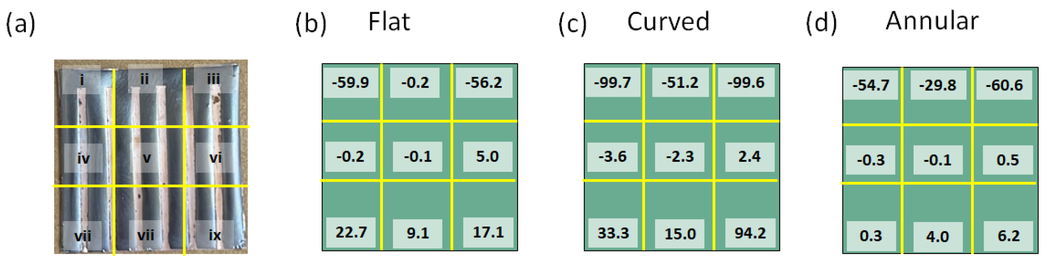
Figure 11.
Measurement results of the magnetic flux density profiles along the strip of the patterned CoNiP magnets after (a) curved magnetization, and (b) annular magnetization.
Figure 11.
Measurement results of the magnetic flux density profiles along the strip of the patterned CoNiP magnets after (a) curved magnetization, and (b) annular magnetization.
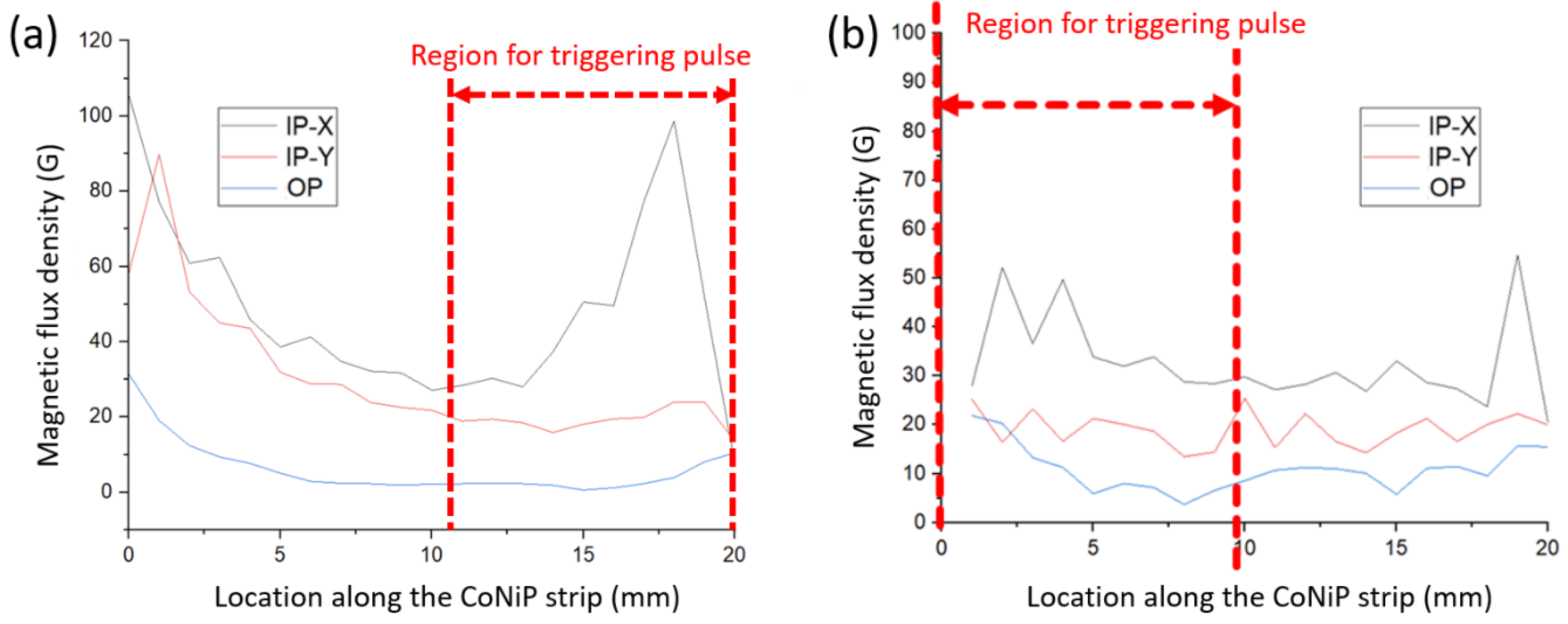
Figure 12.
(a) Output pulses (presented in stacked format) as a function of flight height triggered using the strip region of the patterned CoNiP magnet by curved magnetization. (b) Comparison of the optimal output pulses (presented in stacked format) triggered by the NdFeB and the patterned CoNiP magnets.
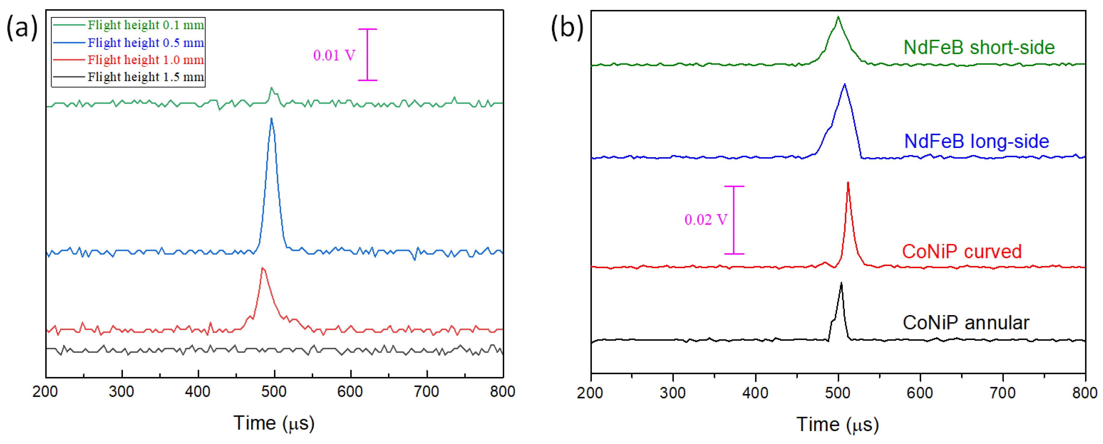

Table 1.
The bath compositions and depositing parameters for the electrodeposition of CoNiP magnet.
| Bath formulation | Composition | Concentration (mole/L) |
| CoNiP | CoCl2·6H2O | 0.2 |
| NiCl2·6H2O | 0.2 | |
| NaH2PO2·H2O | 0.3 | |
| H3BO3 | 0.4 | |
| NaCl | 0.7 | |
| Electrodeposition | Deposition parameter | Settings |
| Galvanic deposition | Bath volume | 400 ml |
| pH value | 4.2 | |
| Current density (CD) | 20 mA/cm2 | |
| Temperature | 25°C | |
| Agitation | Air bubbling |
Table 2.
Properties of the Wiegand element acquired from the commercial WG631 Wiegand sensor.
| Properties of Wiegand element | External field (G) | Pulse FWHM (μs) | Frequency (kHz) | Working temperature (°C) |
| Nominal minimum | 55 | 10 | 0 | -40 |
| Nominal maximum | 120 | 30 | 5 | 125 |
Table 3.
Characterization results showing the hard magnetic properties in the in-plane and out-of-plane directions of the electrodeposited CoNiP magnets.
Table 3.
Characterization results showing the hard magnetic properties in the in-plane and out-of-plane directions of the electrodeposited CoNiP magnets.
| Direction of characterization | Hci (Oe) | Ms (G) | Hc (Oe) | Br (G) | (BH)max (MGOe) |
| In-plane | 1412 | 18050 | 1083 | 4218 | 1.16 |
| Out-of-plane | 1803 | 14550 | 1050 | 2482 | 0.65 |
Disclaimer/Publisher’s Note: The statements, opinions and data contained in all publications are solely those of the individual author(s) and contributor(s) and not of MDPI and/or the editor(s). MDPI and/or the editor(s) disclaim responsibility for any injury to people or property resulting from any ideas, methods, instructions or products referred to in the content. |
© 2023 by the authors. Licensee MDPI, Basel, Switzerland. This article is an open access article distributed under the terms and conditions of the Creative Commons Attribution (CC BY) license (http://creativecommons.org/licenses/by/4.0/).
Copyright: This open access article is published under a Creative Commons CC BY 4.0 license, which permit the free download, distribution, and reuse, provided that the author and preprint are cited in any reuse.


