
Submitted:
25 April 2023
Posted:
26 April 2023
You are already at the latest version
Abstract
Luminescent properties of epitaxial Cu2O thin films were studied in 10-300 K temperature range and compared with luminescent properties of Cu2O single crystals. Cu2O thin films were deposited epitaxially by the electrodeposition method on either Cu or Ag substrates at different processing parameters, which determined the epitaxial orientation relationships and encapsulated surface. Cu2O (100) and (111) single crystal samples were cut from a crystal rod grown by the floating zone method. Luminescence spectra of thin films contain the same emission bands as single crystals around 720, 810 and 910 nm, characterizing VO2+, VO+ and VCu defects, correspondingly. Additional emission bands, whose origin is under discussion, are observed around 650-680 nm, while the exciton features are negligibly small. The relative mutual contribution of the emission bands varies depending on the particular thin film sample. Existence of the domains of crystallites with different orientation determines the polarization of luminescence. PL of both Cu2O thin films and single crystals is characterized with negative thermal quenching in the low temperature region, the reason of this phenomenon is discussed.
Keywords:
cuprous oxide
; single crystal
; epitaxial thin films
; electrodeposition
; photoluminescence
; optical absorption.
1. Introduction
Cuprous oxide Cu2O is known as a p-type semiconductor material with a direct band gap around 2.1 eV. Cu2O crystal has a cubic structure of the space group Pn3m; the primitive cell contains 2 Cu2O units characterized with a lattice parameter 4.27 Å [1]. Historically this material was famous for fundamental investigations of hydrogen-like exciton series, their properties and Bose-Einstein condensation [2,3,4]. The p-type conductivity of this oxide is caused by presence of negatively charged copper vacancies VCu, which are electron acceptors. At present this material attracts great interest for its potential applications on solar energy conversion and photocatalysis at a low production cost [5] due to its favorable qualities such as high absorption coefficient, suitable band gap width, non-toxicity and abundant reserves on Earth. Besides, it can be widely used in various devices such as thin film transistors, smart windows, IR detectors, optical limiters, spintronics, gas and glucose sensing and others [6-7 and references therein].
To implement the application tasks, the mass production of high-quality Cu2O thin films with reproducible properties is necessary. Various methods have been used to deposit Cu2O thin films, such as thermal oxidation, reactive sputtering, chemical vapor deposition (CVD), pulse laser deposition (PLD), molecular beam epitaxy (MBE) and electrodeposition [8,9,10,11,12,13,14,15,16,17]. Except a few cases of films grown by epitaxial techniques such as CVD, PLD and MBE, Cu2O thin films prepared by thermal oxidation, sputtering and electrodeposition are typically polycrystalline containing grains of 50 to 500 nm in size. The electrical and optical properties of the thin films are therefore strongly influenced by the production method which determines the microstructure and defect types as well as their amount. [6,18,19]. It is known that abundant localized states are present at grain boundaries. The undesirable states can be eliminated by growing thin films in an epitaxial form. However, the above mentioned techniques for epitaxial growth require high temperature and high facility expense [11,12,13,14]. One exception is that the epitaxy of Cu2O has been realized by electrodeposition [20]. As many as five orientation relationships between Cu2O and Ag substrate were recently identified by employing a combinatorial substrate approach and epilayers containing low dislocation densities were obtained [21].
Besides the microstructural defects resulted from thin film deposition, the photovoltaic and photocatalytic properties of Cu2O are also affected strongly by the orientations or exposed surface facets of the films. The electrical conductivity, photovoltaics, photocatalysis and thermoelectricity properties of Cu2O are all found to be facet-dependent [22,23,24]. Under the circumstances, it is worth examining whether the anisotropic facet effect is present in the photoluminescence (PL) characteristics. The present study therefore deals with spectral characterization of Cu2O single crystals and epitaxial thin films produced by the electrodeposition method, of various orientations and exposed facets. Results indicate that the PL properties of Cu2O are dominated by the process-related defects rather than facets.
2. Materials and Methods
Cu2O single crystal bar of 7 mm in diameter was grown using the floating zone method. Two samples of 1 mm in thickness, with (100) and (111) polished surfaces, respectively, were cut from the single crystal bar. The single crystals are designated as sample SC(100) and SC(111), respectively, hereafter.
Five thin film samples were prepared by the electrodeposition method in aqueous solutions containing 0.4 M cupric sulfate (CuSO4·5H2O, 99.5% purity) and lactic acid (CH3CH(OH)COOH, 90% purity). The electrolyte was adjusted to a pH value of 9 or 12 by sodium hydroxide (NaOH, 99% purity). The electrodeposition was carried out in a three-electrode system using a Metrohm Autolab PGSTA204 potentiostat in either a potentiostatic or galvanostatic condition at 60oC. The electrolyte and deposition conditions of the Cu2O samples are listed in Table 1. The deposited films were analyzed by X-ray diffraction (XRD, Bruker D8 Discover) and secondary electron microscopy (SEM, Zeiss Supra 55). As will be demonstrated later, these five samples have different orientation/facet combinations which allow the anisotropy effect on PL property to be examined in detail. Samples 13, 30, 39 and 40 have Ag polycrystalline substrate, a sample 111 has a (111) Cu single-crystal substrate.
Optical absorption spectra were measured with spectrophotometer Specord 210 (AnalytikJena). Cu2O crystal samples were put in the of a closed cycle refrigerator (CCS-100/204, Janis Research Corporation), providing 10-300 K temperature range, which in its turn was inserted into the spectrophotometer sample camera. The samples on metal substrates are nontransparent, so they were measured at room temperature the integrating sphere with spectral range 380–1100 nm.
Photoluminescence spectra (PL) were measured under excitation with 532 nm laser line using two luminescence-recording systems. Thin films were studied using a set-up containing a grating monochromator (Andor Shamrock SR-303i-B) together with the CCD camera (Andor DV 420A-BU2). The laser excitation light of laser diode 532 nm (Class IIIb) was focused on a spot around 3 mm2. This luminescence set-up was used also for studies of luminescence polarization. For that purpose, a wire grid polarizer (WP 25M—UB, Thorlabs), operating as a polarization analyzer, was inserted in the luminescence beam and a quartz-wedge achromatic depolarizer (DPU-25, Thorlabs) was located before the slit of the polarization-sensitive grating spectrometer in order to depolarize the entering light. The laser, whose emission light is polarized, was positioned with the (electrical component) polarization vector vertical in relation to the sample surface. Luminescence polarization of Cu2O thin films was analyzed turning the analyzer by every 45 degrees. A narrow spectral feature at 810 nm and undulations in the long wavelength region, seen in all spectra obtained on this set-up, are due to the irremovable peculiarities of the equipment.
PL spectra of the crystal samples were recorded with a triple grating Raman spectrometer (TriVista 777) fitted with Peltier cooled CCD detector. The Nd/YAG laser radiation second harmonic was focused on the area of several microns on the sample and luminescence light was collected using the microscope (Olympus BX53). The spectral resolution of luminescence detection was 0.1 nm. Temperature was controlled by temperature controller (Lake Shore 331), that provided temperature stability of 0.1 K. In this set-up the laser power was varied by two orders of magnitude in order to detect the spectral changes produced by the rise of the excitation power. Metal wire cloth was used in front of the luminescence detection system to prevent its oversaturation when using the high laser excitation power. Measurement temperature in the 10-300 K range was provided by using a closed cycle helium cryostat model DE-204. All necessary apparatus spectral corrections were done.
3. Results
3.1. Microstructure
Figure 1 shows the SEM micrographs and XRD patterns of samples 13, 30, 39 and 40, electrodeposited on Ag polycrystalline substrates. All the low-magnification SEM micrographs shown in Figure 1a,d,g,j reveal a clear grain-based contrast. In other words, the film deposited on each substrate grain has a specific brightness, indicating that the morphology of the deposited film is affected strongly by the orientation of the substrate grain. This orientation-dependent contrast provides an evidence that the films are likely deposited epitaxially [21,25]. Moreover, the SEM micrographs at high magnifications (Figure 1b,e,h,k) acquired from the squared area in the corresponding low-magnification micrographs show that the films are composed of crystals oriented in the same manner, confirming the hypothesis of epitaxy. Accordingly, most of the films were deposited epitaxially on their underlying substrate grains. The epilayer deposited on a specific substrate grain is thus called a domain hereinafter. It is known that the Cu2O crystals have either {111} or {100} habit planes depending on the depositing conditions. In the present case, the SEM micrographs in Figure 1e,k, for samples 30 and 40, respectively, show that the crystals are encapsulated by {100} planes. In Figure 1b,h, no clear habit planes can be identified. With the assistance of the crystals grown on other areas (results not shown), the crystals in samples 13 and 39 have {111} habit planes. In addition, the XRD patterns for theses samples are shown in Figure 1, (c), (f), (i) and (l), respectively, to revel the preferred orientation of the deposited films. The intensity ratios among peaks of Cu2O should be roughly the same as those of Ag if the films were all grow epitaxially based on a cube-on-cube orientation relationship (OR). However, it is worth mentioning that at least four more ORs were identified between Cu2O and Ag in addition to the expected cube-on-cube OR [21]. Therefore, the intensities of the Cu2O peaks vary from one sample to another. The grain orientation is expressed as an <hkl>//ND notation; here ND represents the normal direction of the sample surface. Both samples 13 and 30 possess a strong <111>//ND texture, whereas sample 39 has a <220>//ND + <200>//ND texture and sample 40, on the other hand, has a <220>//ND + <111>//ND texture. The texture and crystal facet planes for these samples are given in Table 2.
Figure 2 shows the XRD analytical results for sample 111, for which a (111) Cu single crystal substrate was used. The diffraction pattern in Figure 2 acquired in a ω/2θ configuration shows a (111)Cu2O peak at 36.62o and a very weak (200)Cu2O peak at 42.39o in addition to a strong (111)Cu peak, indicating that an (111) epilayer was deposited. According to the (111)Cu2O rocking curve in the inset, the peak has a full width at half maximum (FWHM) of 1.36o. Considering that the FWHM of the (111)Cu rocking curve is about 0.3o, the crystallinity of the epilayer is only slightly worse than those prepared by the high vacuum, high temperature processes such as molecular beam epitaxy (FWHM=0.52o in [26]). Figure 2, (b) shows the phi scans of the (200)Cu and (200)Cu2O peaks, revealing that the epilayer contains a small fraction of a <111>/60o twin variant. The SEM micrograph in the inset shows that the twin crystals can be identified in the epilayer as highlighted by the dashed triangles. Scattered crystals in a square shape enclosed by four {111} habit planes were observed occasionally on the surface of the epilayer (result not shown). These crystals have a <100>//ND orientation, corresponding well with the very weak peak present Figure 2, (a) at 2θ=42.3o. The (111) epilayer therefore exhibits mainly a smooth (111) surface.
3.2. Absorption
Absorption spectra were measured to estimate the optical band gap values for Cu2O samples. Absorption spectra of Cu2O single crystals show a band edge around 600 nm (2.07 eV) at 10 K, which is sequentially moved towards lower energies with temperature rise up to 640 nm (1.94 eV) at RT, see Figure 3, (a) and (b). Elements of fine structure are seen in the absorption spectra of Cu2O crystals at 582 nm (2.13 eV) (SC(111) and SC(100) samples) and 548 nm (2.26 eV) (sample SC(111)) at the lowest temperature.
Cu2O thin samples are electrodeposited on metallic substrates, which are not transparent. For these samples diffuse reflection spectra were measured by means of the integrating sphere inserted in the spectrophotometer sample camera at RT and converted into absorption spectra. Due to the small thickness of Cu2O film, the obtained spectrum contained the features of both Cu2O layer and substrate metal, constituting a combined spectrum. To obtain Cu2O thin films absorption spectrum, the absorption spectrum of a metal substrate was measured and subtracted from the combined spectrum. As a result of this procedure absorption spectra of Cu2O thin films are obtained with a large amount of inaccuracy. Examples of such residual spectra are shown in Figure 3, (c and d) for the samples 13 and 39.
For the calculations of the band gap value the widely used Tauc procedure [17,27] was applied. The band gap values were determined for all the studied Cu2O samples, applying the Tauc plot to the absorption curves: (λhν)2 versus photon energy hν (not shown here graphically). The photon energy and absorption coefficient are linked to band gap energy Eg by relation:
where K is a constant. From the Tauc plot, the band gap value was determined as an intersection point of the tangent to a curve with an abscissa. The obtained band gap values for all Cu2O samples are shown in Table 3.
3.3. Photoluminescence
3.3.1. Cu2O Single Crystals
Photoluminescence measurements were performed for two single-crystal samples of Cu2O, cut in (111) and (100) directions from the same crystal rod. PL excitation was done by the 532 nm laser applying two values of radiation power, which varied by about two orders of magnitude: 0.2 and 15 mW. PL spectra for two single crystal samples are shown in Figure 4, corresponding to the low laser power on the top figures, and to the high laser power–on the bottom figures. The luminescence bands observed are related to the following defects: 609 nm (2.04 eV)–with an exciton, 720 nm (1.72 eV)–with a doubly charged oxygen vacancy VO2+, 812 nm (1.53 eV)–with an oxygen vacancy VO+, and 910 nm (1.36 eV)–with a copper vacancy VCu. (The peak positions hereafter will be titled as detected at 10 K temperature). Similar emission bands were observed and assigned by other authors [28,29,30] with reminder that the exact peak position and relative intensities depend on the used growth procedure and sample treatment.
Exciton band at around 610 nm assigned to the yellow 1s ortho-exciton occurring due to electric quadrupole transition and denoted as (Y 1s) followed with phonon side bands due to the electric dipole transitions and its evolution with temperature rise has been widely studied [28,31,32]. In the present paper we will not focus on investigation of the exciton emission band.
The relative contribution of the bands to the PL emission spectra depends on the sample. Thus, under the lower excitation light power for sample SC(111) (Figure 4a), the 910 nm band dominates, the 720 nm band is very weak and other bands are negligible small. At the same time, for the sample SC(100) (Figure 4c) intensity of the 720 nm band is comparable with that of the 910 nm band, while the 610 nm and 812 nm bands become observable. Increase of the excitation light power causes essential increase of the shorter wavelength bands’ intensity for both crystal samples, as it is seen in Figure 4b,d.
The variations of the Cu2O single-crystal spectra with temperature rising up to RT were studied as follows. (1) Band positions demonstrated a red shift of 0.055 ± 0.005 eV according to the thermal narrowing of the band gap, whereas the dependence on the excitation power was not observed, see Figure S1 (Supplementary Material). (2) Emission bands are subjected to thermal quenching with different rate: the 812 nm band disappears at around 100 K, the 720 nm band—at around 200 K, while the 609 and 910 nm bands survive up until RT.
In both Cu2O single crystal samples all the observed emission bands demonstrate a complicated behavior with temperature rise: at first emission intensity increases, then attains plateau, and at critical temperature T0 begins to decease, as shown in Figure 5(a). The phenomenon of luminescence intensity increase with temperature rise is called negative thermal quenching (NTQ) [33, 34 and references therein], anomalous thermal quenching [35] or antiquenching [36]; the notion of critical temperature is introduced by Rechnikov [33]. It was observed that in the studied Cu2O single crystals value of critical temperature T0 varies in the 20-55 K limits depending on the sample, particular emission band and excitation light power.
In the present paper the temperature dependence and the corresponding Arrhenius plot are shown graphically for the most intensive 720 and 910 nm bands of sample SC(111), see Figure 5 (a and b). For the 910 nm band T0 is shifting from 20 K under the higher excitation power (Figure 5, (a), curve 1) to 50 K under the lower excitation power (Figure 5, (a), curve 3), whereas for the 720 nm band T0 varies from 35 to 55 K (Figure 5, (a), curves 2 and 4). At higher temperatures the corresponding curves drift together. Similar luminescence behavior is observed in sample SC(100).
Arrhenius plot (Figure 5, (b)) enables estimation of the activation energies Ea for the 910 and 720 nm emission. Activation energy can be found from the Mott-Seitz equation [37],
where I0 and I(T) and are luminescence intensities at temperatures 0 and T, k is Boltzmann constant and a is a frequency factor, determined by ratio of radiative τR and nonradiative lifetimes τNR: a=τR/τNR.
The obtained corresponding Ea values are shown in Table 4, together with those for other samples.
Similar values of activation energies are obtained for both crystal samples: 80–90 meV for the 720 nm band and 135–150 meV for the 910 nm band. The values increase under rise of the excitation power to 90–100 meV and 190–200 meV, correspondingly.
3.3.2. Cu2O Thin Films
Five Cu2O thin film samples were studied for luminescence properties, varied for the substrate type and production conditions, which are listed in Table1. PL spectra in 10–300 K temperature range, their dependence on illumination spot position and luminescence polarization were examined.
For all studied Cu2O thin films independently of sample structure (texture and facet plane) the PL spectrum looks like a broad structured band in the 640–1050 nm spectral region with a peak position varying in the 650–750 nm limits. The emission subbands characteristic to bulk single crystal Cu2O can be distinguished, they are somewhat red-shifted (to 735, 820 and 920 nm at 10 K), diffuse and overlapping. Spectral positions of the PL subbands were determined by curves deconvolution into Gaussian components, not shown graphically. Besides, new features appear at 660 nm (in some samples), 680 and 960 nm. Exciton emission around 610 nm is not observed even at the lowest temperature. Contrary to the bulk crystalline samples the 910 nm emission band is rather weak.
The characteristic feature of Cu2O thin films is the dependence of the PL spectra shape on the illumination spot position during detection of the luminescence signal. Movement of the excitation spot over the surface causes the changes in the spectrum peak position as well as in the luminescence intensity.
The summary of the normalized PL spectra of Cu2O thin films obtained under excitation 532 nm at random surface places is given in Figure 6, curves 1–5; for comparison PL spectra of the crystalline bulk sample (100) is also shown (Figure 6, curve 6).
Luminescence polarization measurements have shown that the shape of PL spectra of thin films depend on the angular position of the analyzer, confirming the presence of the luminescence polarization. It should be mentioned that spectra of polarized luminescence also vary depending on illumination spot location on the sample surface.
To characterize the thermal behavior of the thin film PL at different wavelengths, intensity of each subband integrated over the spectral range (λmax ± 10) nm was plotted versus temperature. Arrhenius plot was built, activation energies were estimated similarly to the case of single crystals and listed in Table 4.
The further result description is structured according to the individual samples.
Sample 111 is a 1.0 μm thick Cu2O epilayer on substrate of single crystal Cu (111). It was observed that movement of the illumination spot along the surface of the sample 111 did not cause the observable changes in the spectrum shape. Maximum of its PL spectrum at 10 K is found at 735 nm (Figure 7a). With temperature rise the PL intensity first increases up to 30 K, then decreases up to RT. Emission subbands constituting the PL spectrum, are subjected to thermal quenching with different rates.
Dependence of the integral intensity of the subbands 680, 735, 820 and 920 nm on temperature is shown in the Figure 8a, while its Arrhenius plot is shown in the Figure 8b. All subbands demonstrate NTQ up to T0 = 30 K. With temperature increase, first quenches the 680 nm, then the 735 nm band, and the 820 and 920 nm bands survive up to RT. The descending parts of the Arrhenius curves cannot be approximated with single straight lines, making determination of activation energy values inaccurate. Roughly estimated values of activation energies for the PL subbands are listed in the Table 4.
PL polarization measurements confirm the presence of polarized emission of the thin film sample 111; for the particular sample position the relative contribution of the 680, 820 and 920 nm bands is lowest at the analyzer angular degree 0°, and highest at 90° position (see Figure 7b).
Sample 13 is a 8.7 μm thick Cu2O film on polycrystalline Ag substrate; its texture is characterized as <111>//ND and habit plane as {111}. PL spectrum of this sample has a peak, whose position varies in a wide spectral range depending on the chosen location of the illumination spot. For the particular chosen location the spectrum maximum is at 700 nm at 10 K (Figure 9a). As seen from Figure 10a,b, neither emission subband demonstrates NTQ, the PL intensities decrease monotonously beginning from 10 K. After thermal quenching of the 680 and 735 nm subbands the PL spectrum at RT contains the 820 and 920 nm subbands. The obtained activation energies for emission bands are listed in the Table 4.
Polarized luminescence for this sample was measured only in the 600–800 nm spectral range (Figure 9b) because of the insufficient emission intensity at higher wavelengths. Faint signs of polarized luminescence are seen as the irregular thickening of the spectrum overlapping curve.
Sample 30 is a representative of Cu2O thin films on polycrystalline Ag substrate, its thickness is 1.3 μm, texture is characterized with <111>//DF, and habit plane as {100}. The PL spectrum of the sample 30 at the particular chosen illumination spot position has a peak at around 735 nm and a well-expressed shoulder at 680 nm (Figure 11, (a)). With temperature rise the short wavelength subbands are thermally quenched one by one, and at RT the 920 nm subband is left, besides a subband around 960 nm becomes visible.
All emission subbands show NTQ up to T0 = 40 K, as it is seen in Figure 12a. Arrhenius plots for the subbands intensities can be approximated with straight lines (Figure 12b) and activation energies estimated (shown in Table 4).
Polarization measurements (Figure 11b) taken for a random illumination spot on the sample surface confirms presence of the polarized luminescence, expressed mostly in the 680 and 750 nm spectral areas.
Sample 39 is a 1.3 thick Cu2O film on Ag polycrystalline substrate, characterized with texture <200>//ND+<220>//ND and habit plane {111}. It has well-structured subbands at 680, 735, 820 and 920 nm in the PL spectrum (Figure S2, a); all subbands are characterized with NTQ, critical temperature T0 being 20 K for the 680 nm and 40 K for other subbands (Figure S3). Presence of luminescence polarization is pronounced best of all in the spectral regions around 700, 735 and 820 nm (Figure S2, b).
Sample 40 is Cu2O thin film on Ag polycrystalline substrate, its thickness is 1.3 μm, texture <111>//ND+<220>//ND and habit plane is {100}. PL spectrum of this sample has evident subbands at 680 and 660 nm apart from the usual subbands 735, 820 and 920 nm (Figure S4). The 660 and 680 nm subbands thermally quench monotonously and disappear below 100 K. Other subbands show NTQ, the most high-temperature one is the 920 nm subband. It is observable at RT together with the 960 nm subband (Figure S5).
4. Discussion
4.1. Absorption
Optical absorption in Cu2O is determined by the direct transitions from the valence band to the conduction band at the Γ-point of the Brillouin zone. Splitting of the highest valence band and the lowest conduction band results in four types of the allowed fundamental transitions named as yellow, green, blue and indigo according to wavelengths of their spectral positions [28]. Optical band gap, which is determined by the yellow transitions, is mentioned at 2.17 eV [28,29]. Electron transitions are accompanied with the corresponding series of excitonic transitions, observed in the absorption spectra. Exciton absorption lines are seen even at RT in high quality crystals, especially after crystal annealing.
Absorption spectra of single crystals (100) and (111) obtained in the present work (Figure 3a,b), clearly show the thermal shift of the band edge by 0.13 eV in the 10-300 K range and signs of lines from the yellow exciton series at the lower temperature. The values of the optical band gap obtained for both crystals from the Tauc plot, constitutes 2.04 eV at 10 K, which is lower than most of the literature data.
Absorption spectra of Cu2O thin films the obtained from the diffuse reflection spectra and with subtraction of the metal substrate spectrum are not precise and are shown here for two thin film samples for illustrative purpose (Figure 3c,d. The band gap values for Cu2O thin films obtained with the Tauc plot method, range in 1.91-1.99 eV limits, with an error ± 0.05 eV. Such band gaps are in agreement with a very broad range of values for Cu2O thin films, varied depending on production method, substrate type and growth conditions, beginning from 1.92 up to 2.02 eV for samples electrodeposited on glass [38], 2.0 eV for the samples electrodeposited on Au [18], and up to 2.4 eV in the vacuum annealed magnetron sputtered thin films on glass [7,17]. Growth conditions and annealing of thin films play a decisive role in stoichiometry of crystalline structure, determining presence of lattice defects, and the band gap value [6].
4.2. Photoluminescence
4.2.1. Single Crystals
In general, the experimental spectra of Cu2O single crystals, containing emission bands consisting of an exciton (609 nm; 2.04 eV), a doubly charged oxygen vacancy VO2+ (720 nm; 1.72 eV), an oxygen vacancy VO+ (812 nm; 1.53 eV), and an electrically neutral copper vacancy VCu (910 nm; 1.36 eV), see Figure 4a–d, coincide well with the photoluminescence spectrum in the 600–1050 nm spectral range reported previously [28,29,30]. The mentioned energies are observed at low temperature (10 K), and the emission energies decrease as a result of band gap narrowing with increasing temperature. Already in 1980s and later it was suggested that the emission bands of Cu2O natural and synthetic crystals in the 700–1000 nm range are connected with bound excitons localized at oxygen and copper vacancies [4,39,40]. The varied mutual relation is observed between intensities of the emission bands in samples SC(100) and SC(111), seen in Figure 4a,b, which becomes even more pronounced under increased excitation power (Figure 4c,d). The different relative contribution of the defect-related emission bands to the PL spectrum in samples SC(100) and SC(111) cut from the same crystal rod, should be explained rather by the inhomogeneous distribution of the intrinsic defects along the crystal rod created during growth, than by the crystallographic plane of the sample surface.
Intensity of the defect bands at 720, 812 and 910 nm gives no information on relative abundance of the corresponding defects, because the corresponding luminescence centers are characterized with different physical parameters, different exciton localization mechanisms and different luminescence mechanisms [40]. Rise of the excitation power increases the number of excitons and conduction carriers in the crystal, localizing at oxygen and copper vacancies with different efficiency. Thus, in [31] is was supposed, that conduction carriers or other nonthermalized states tend to be trapped at oxygen vacancies, while cold and diffusive excitons tend to excite copper vacancies. From the Figure 4 it is seen that emission of the centers corresponding to oxygen vacancies (the 720 and 812 nm bands) are more sensitive to excitation power increase, than copper vacancies, responsible for the 910 nm band. Dependence of the defect bands’ intensity relation on excitation power confirms the concept of their origin from bound excitons.
In the present work it was observed that all defect emission bands of Cu2O crystal samples are subjected to the negative thermal quenching NTQ, where luminescence intensity increases with temperature rise in some temperature range (see Figure 5a) for the 720 and 910 nm emission bands of the crystal sample (111). Previously NTQ of emission bands was observed in different materials and explained by different mechanisms: in doped GaN–by quenching of a competitive intense luminescence band or a nonradiative channel [34], in sandwiched single layer MoS2–by raising radiative recombination rate of the excess delocalized carriers created from the carrier hopping from the shallow defect states to the band edges [35], in CdMnTe–by participation of intermediate states of impurities in recombination processes, in ZnO and CdMnTe–by presence of intermediate defect states and nonradiative channels [41,42]. Some authors explain NTQ by thermal activation of charge carriers and trapped excitons from shallow traps followed by their localization at radiative centers [31,36,43].
As for Cu2O single crystals, only some researchers have observed NTQ of one or several defect bands in their PL studies [31,44], while others reported regular continuous thermal quenching of emission bands. The latter explanation involving retrapping of bound excitons seems to be the most appropriate for the Cu2O crystals. Most probably, NTQ is observed in those Cu2O crystals, where surface or intrinsic defects create shallow nonradiative levels for localization of bound excitons at low temperatures, which are easily dissociated at temperature rise. Such defects could be produced in crystals under specific growth conditions. Released excitons are retrapped at vacancies, either oxygen or copper; providing increase of emission intensity of the defect-related bands up to attaining the critical temperature; their further thermal behavior follows the normal thermal quenching.
Under increased excitation power critical temperature shifts to higher temperatures for both prominent emission bands 720 and 910 nm, see Figure 5a, the following quenching occurs at different rates but at the final stages the corresponding curves (Figure 5a (curves 1 and 3); (2 and 4)) flow together. Thus, the 720 nm emission band reaches the complete bleaching at 150 K both at low and high excitation power. The Arrhenius plot (Figure 5b) confirms the complicated character of the quenching behavior, and the values of the activation energy can be estimated with a large error (15 %), see Table 4.
4.2.2. Thin Films
Many authors have studied PL spectra of Cu2O thin films, produced by different methods and using different substrates [5,6,17,19,28,38,40,45]. These spectra may be either with or without exciton feature; in some samples the defect bands are well separated, in others–more diffuse and merged into a continuous broad band. Similar to Cu2O single crystals, luminescence bands in thin films are assigned to a doubly charged oxygen vacancy VO2+, an oxygen vacancy VO+, and an electrically neutral copper vacancy VCu, though band positions are shifted compared to their single crystal counterparts. Comparing with PL spectra of single crystal Cu2O samples, thin film spectra are characterized with the higher relative contribution of oxygen vacancy bands. Taking into account the relatively larger contribution of the surface defects in case of thin films containing tiny crystallites, domination of oxygen vacancy-related radiation is in accordance with experimental microscopic observations and computer simulations using density functional theory, which have shown that oxygen vacancy is a prevalent defect on Cu2O surface [46]. Often an additional band in the 650–690 nm region is observed [5,28,31,47], which is not typical for Cu2O crystals and whose origin is not determined, though connection with nitrogen-related acceptor is suggested [5,47]. In [40] the broad structureless spectrum of Cu2O /Au (111) thin films was observed under 532 nm; it was suggested to be related with interface plasmons, stimulated by Cu2O excitons, which migrate to the metal/oxide boundary. No information of the NTQ observations in thin film samples was found in literature.
Summarizing the results on PL characteristics under 532 nm laser excitation of the studied Cu2O thin films electrodeposited on metal substrates, the general similarity of their PL spectral and thermal properties is observed independently of the film orientation and facet plane and provided by presence of intrinsic defects. The exciton band around 610 nm is not observed or is negligibly small, the defect-related luminescence is presented with a broad structured spectrum in the 630-1050 nm spectral range with a dominating part in 650-750 nm region, corresponding mainly to VO2+ band. The structure of emission bands allows distinguishing of the common bands related to a doubly charged oxygen vacancy VO2+, an oxygen vacancy VO, and an electrically neutral copper vacancy VCu. Besides, the additional bands are observed at 680 nm (1.82 eV) and 660 nm (1.88 eV), especially well pronounced in samples 13, 30, 40 (Figure 6).
Most of the thin film samples, with exception of the sample 13, demonstrate NTQ in the low temperature region, critical temperature T0 occurring at 30-40 K. It can be supposed that NTQ in Cu2O thin films has the same origin as that in single crystals and relates to excitons delocalization from shallow trap levels and localization at oxygen and copper vacancies at temperature rise. During the following regular thermal quenching due to temperature rise emission subbands disappear one after another beginning with the shortest wavelengths and ending with the longest wavelengths, so that at RT mainly 900-1000 nm emission is left. From the Arrhenius plots for the studied samples, which are not described by single straight lines for most of the studied thin films, it follows that the thermal quenching is governed by a combined process, and only rough estimation of the activation energies can be done, especially for the VCu band at 920 nm. Values of activation energy for the thin films are given in Table 4.
Cu2O thin films layers (13, 30, 39, 40) on Ag polycrystalline substrates demonstrate dramatic changes in spectrum shape with shift of the excitation spot and polarized luminescence mainly in the 650-850 nm region. Dependence of the PL spectra shape on the excitation spot on a sample surface and luminescence polarization features are in accordance with the domain structure of Cu2O thin films, which is seen in the SEM micrographs photos (Figure 1). Similarly oriented Cu2O crystallites of few microns size of cubic and pyramidal shape are arranged in domains of tens micrometer size. Excitation spot of ≈ 3 mm2 covers several crystalline domains. Spectrum shape and polarization of the detected luminescence signal is therefore determined by the radiative defects in the irradiated domains. It has been demonstrated in [21], that each domain in a Cu2O sample contains different density of grown-in dislocations. The densities of radiative defects may also be different in domains. It explains why the PL spectra shape varies from on position to another. These facts allow proposal of chaotic distribution of domains with crystallites of different orientations and different mutual relations of luminescence bands. Irregular structure of polycrystalline metal substrate determines irregularities of Cu2O crystalline structure.
Sample 111 shows the minimal dependence of the spectrum shape on the shift of the excitation spot and at the same time the most expressive polarization features along the whole spectrum (Figure 7b), speaking in favor of uniform distribution of similar crystallites along the surface of the sample. Evidently, the regular crystal structure of Cu crystal determines regularity of Cu2O crystallites.
Properties of the 660 and 680 nm emission bands, seen is PL spectra of Cu2O thin films, manifested in thermal behavior and luminescence polarization show their similarity to VO2+ emission band at 735 nm. It implies that the 660 and 680 nm emission bands may be related to bound excitons localized at oxygen defects distorted by crystallite surface, grain boundaries, and dislocations or other extended defects, generating local electric fields and being produced during thin film growth. Similarly, the long wavelength band at around 960 nm, seen in Cu2O thin films at RT, might be related to distorted copper vacancies, though additional studies are required for its assignment.
5. Conclusions
Spectral properties of Cu2O (100) and (111) single crystals, grown by floating method, and Cu2O thin films, deposited by electrodeposition, with various orientations and facets were studied under laser excitation 532 nm in 10-300 K temperature range. Optical band gap value of the Cu2O single crystal samples was estimated from the absorption spectrum as 2.04 eV. Similarly to other reported data, PL spectra of the studied Cu2O single crystal samples contain the Y1 exciton emission band (609 nm; 2.04 eV) with phonon sidebands and emission bands related to a doubly charged oxygen vacancy VO2+ (720 nm; 1.72 eV), an oxygen vacancy VO+ (812 nm; 1.53 eV), and an electrically neutral copper vacancy VCu (910 nm; 1.36 eV). The negative thermal quenching of defect-related emission bands observed in low temperature region (up to critical temperature T0 20–50 K) is presumably explained by the release of bound excitons from the shallow traps due to lattice structure defects generated during crystal growth and retrapping of bound excitons to oxygen and copper vacancies. Presence of NTQ confirms the concept of the defect bands origin related to bound excitons. Increase of excitation power by two orders of magnitude causes the non-proportional rise of the emission bands related to oxygen vacancies, decrease of the critical temperature and activation energy of regular thermal quenching of VO2+ and VCu emission bands.
For the Cu2O thin film samples, the rough estimation of optical band gap showed values in 1.91-1.99 eV region at RT. PL properties of the studied Cu2O thin films are determined by the presence of the intrinsic defects in crystalline lattice but not the sample orientation and facet plane. Contrary to single-crystal counterparts, PL spectra of the studied thin films contain no exciton band, while the defect-related region is presented with a broad structured band in 650-1050 nm region, where besides the distinguished diffused VO2+ (735 nm, 1.69 eV), VO+ (820 nm, 1.51 eV) and VCu (920 nm, 1.35 eV) bands, additional bands are observed at (660 nm, 1.88 eV–in some samples), 680 nm (1.82 eV) and 960 nm (1.3 eV) . Under temperature rise for most of the samples NTQ is observed for the emission bands at low temperature up to T0 30-40 K, followed by normal thermal quenching. Rising temperature causes emission fading beginning the short wavelength side. Similarity of spectral and thermal properties of PL of Cu2O thin films with those of single crystals allows their assignment to emission of bound excitons localized at oxygen and copper vacancies and other structural defects.
Dependence of the PL spectrum shape on position of the excitation spot and presence of the luminescence polarization is in line with domain structure of thin films, containing crystallites of different orientations and presumably having different defects. Cu2O epitaxial layer on Cu single crystal (111) stays apart from other samples on polycrystalline metal substrates due to its regular structure, manifested in the polarized luminescence spectrum and spectrum independence on the excitation spot.
Supplementary Materials
The following supporting information can be downloaded at: Figure S1. Peak position of the main emission bands of Cu2O single crystals (100) and (111) under laser excitation power 0.2 and 15 mW in 10-300 K temperature range; Figure S2. Spectral properties of Cu2O thin film on Ag polycrystalline substrate (sample 39) under 532 nm laser excitation: (a) Thermal evolution of PL spectra; (b) polarized PL spectra at different angular positions of the analyzer at 10 K; Figure S3. Thermal evolution of PL subbands for thin film sample 39: (a) PL intensity; (b) Arrhenius plot; Figure S4. Thermal evolution of PL spectrum of Cu2O thin film on Ag polycrystalline substrate (sample 40) under 532 nm laser excitation; Figure S5. Thermal evolution of PL subbands for thin film sample 40: (a) PL intensity; (b) Arrhenius plot.
Author Contributions
Conceptualization, L.T., L.C.; methodology, L.T., L.C., D.D. and B.B; validation, L.T., D.D. and L.C.; investigation, T-Y. W., J.G., D.N., R.R. and R.N.; resources, L.T. and M.M.-C.C.; data curation, T-Y.W.and D.N.; writing—original draft preparation, L.T. and L.C.; writing—review and editing, L.T., L.C., B.B., M.M.-C.C. and R.N.; visualization, L.T., D.D. and L.C.; supervision, L.C. and L.T.; project administration, L.T., L.C. and M.M.-C.C.; funding acquisition, L.T. and and M.M.-C.C. All authors have read and agreed to the published version of the manuscript.
Funding
The financial support of M-ERA.NET project “ZnMgO materials with tunable band gap forsolar-blind UV sensors” (ZMOMUVS) and the post-doctoral research project “Growth and characterisation of Ga2O3 and ZnMgO thin films for solar-blind ultraviolet applications” (R. Nedzinskas; research application no.: 1.1.1.2/VIAA/3/19/442) is acknowledged. Institute of Solid State Physics, University of Latvia as the Center of Excellence has received funding from the European Union’s Horizon 2020 Framework Program H2020-WIDESPREAD-01-2016-2017-TeamingPhase2 under Grant Agreement No. 739508, project CAMART2. The electrodeposition and related characterization works were also supported by the Ministry of Science and Technology of the Republic of China (MOST 107-2221-E-110 -004 -MY3).
Institutional Review Board Statement
Not applicable.
Informed Consent Statement
Not applicable.
Data Availability Statement
The raw/processed data required to reproduce these findings cannot be shared at this time as the data also form a part of an ongoing study.
Conflicts of Interest
The authors declare no conflict of interest. The funders had no role in the design of the study; in the collection, analyses, or interpretation of data; in the writing of the manuscript, or in the decision to publish the results.
References
- JCPDS file: 04–007-9767.
- M. Hayashi and K. Katsuki, Hydrogen-Like Absorption Spectrum of Cuprous Oxide. J. Phys. Soc. Jpn. 7 (6) (1952) 599-603. [CrossRef]
- J. Li, Z. Mei, D. Ye, H.Liang, L.Liu, Y. Liu, A. Galeckas, A.Y. Kuznetsov and X. Du, Engineering of optically defect free Cu2O enabling exciton luminescence at room temperature. Optical Materials Express 3(12), (2013) 2072-2077. [CrossRef]
- T. Ito, T. Masumi, Detailed examination of relaxation processes of excitons in photoluminescence spectra of Cu2O. J. Phys. Soc. Jpn. 66 (1997) 2185-2193. [CrossRef]
- J. Li, Z. Mei, L. Liu, H. Liang, A. Azarov, A. Kuznetsov, Y. Liu, A. Ji, Q. Meng and X. Du, Probing defects in nitrogen-doped Cu2O. Sci. Rep. (2014) 4:7240. [CrossRef]
- I. S. Brandt, M. A. Tumelero, S. Pelegrini, G. Zangari, A. A. Pasa, Electrodeposition of Cu2O: growth, properties, and applications. J. Solid State Electrochem. 21 (2017) 1999-2020. [CrossRef]
- D. Murali, S. Kumar, R. J. Choudhary, A.D. Wadikar, M. K. Jain, A. Subrahmanyam, Synthesis of Cu2O from CuO thin films: Optical and electrical properties. AIP Advances 5 (2015) 047143. [CrossRef]
- T. K. S. Wong, S. Zhuk, S. Masudy-Panah and G. K. Dalapati, Current status and future prospects of copper oxide heterojunction solar cells. Materials, 9 (2016) 271. [CrossRef]
- H. A. Al-Jawhari, A review of recent advances in transparent p-type Cu2O-based thin film transistors, Mater Sci Semicond Process 40 (2015) 241–252. [CrossRef]
- L. C. Chen, Review of preparation and optoelectronic characteristics of Cu2O-based solar cells with nanostructure, Mater Sci Semicond Process 16 (2013) 1172–1185. [CrossRef]
- H. H. Yeh, M. C. Wen, L. Chang, K. H. Ploog, M. M. C. Chou, Epitaxial growth of Cu2O on Cu substrate–A combinatorial substrate approach, J. Cryst. Growth, 512 (2019) 124-130. [CrossRef]
- H. Kobayashi, T. Nakamura, N. Takahashi, Preparation of Cu2O films on MgO (1 1 0) substrate by means of halide chemical vapor deposition under atmospheric pressure, Mater. Chem. Phys., 106 (2007) 292–295. [CrossRef]
- Y. Wang, J. Ghanbaja, F. Soldera, P. Boulet, D. Horwat, F. Mücklich, J.F. Pierson, Controlling the preferred orientation in sputter-deposited Cu2O thin films: Influence of the initial growth stage and homoepitaxial growth mechanism, Acta Mater. 76 (2014) 207–212. [CrossRef]
- X. Liu, M. Xu, X. Zhang, W. Wang, X. Feng, A. Song, Pulsed-laser-deposited, single-crystalline Cu2O films with low resistivity achieved through manipulating the oxygen pressure, Appl. Surf. Sci., 435 (2018) 305–311. [CrossRef]
- H. H. Yeh, M. C. Wen, L. Chang, K. H. Ploog, M. M. C. Chou, Epitaxil growth of Cu2O on Cu substrate–a combinatorial substrate approach. J. Cryst. Growth 512 (2019) 124-130. [CrossRef]
- T. Ha, I. Park, K. I. Sim, H. Lee, J-S. Bae, S. J. Kim, J. P. Kim, T-T. Kim, J. I. Jang, S-Y. Jeong, Single-crystalline Cu2O thin films of optical quality as obtained by the oxidation of single-crystal Cu thin films at low temperature. APL Mater. 7, 031115 (2019). [CrossRef]
- M. Elmahdy, A. El-Shaer. Structural, optical and dielectric investigations of electrodeposited p-type Cu2O. J. Mater Sci Mater Electron 30 (2019) 19894-19905. [CrossRef]
- M. Izaki, S. Sasaki, F. B. Mohamad, T. Shinagawa, T. Ohta. S. Watase, J. Sasano, Effects of preparation temperature on optical and electrical characteristics of (111)-oriented Cu2O films electrodeposited on (111)-Au film. Thin Solid Films 520 (2012) 1779-1783. [CrossRef]
- Y. L. Liu, Y. C. Liu, R. Mu, H. Yang, C. L. Shao, J. Y. Zhang, Y. M. Lu, D.Z. Shen and X. W. Fan, The structural and optical properties of Cu2O films electrodeposited on different substrates. Semicond. Sci. Technol. 20 (2005) 44-49. [CrossRef]
- E. W. Bohannan, M. G. Shumsky, and J. A. Switzer, Epitaxial electrodeposition of copper (I) oxide on singlecrystal gold(100). Chem. Mater. 1999, 11, 2289-2291. [CrossRef]
- D. Dai, P.-Y. Huang, T.-Y. Wu, C.-H. Shih and L. Chang, Epitaxial electrodeposition of Cu2O on Ag substrates in sulfate baths, J. Cryst. Growth, 603 (2023) 126983. [CrossRef]
- S. Sun, L. He, M. Yang, J. Cu, and S. Liang, Facet junction engineering for photocatalysis: a comprehensive review on elementary knowledge, facet-synergistic mechanisms, functional modifications, and future perspectives, Adv. Funct. Mater. 2022, 32, 2106982. [CrossRef]
- Y. Li, K. Luo, R. Tao, Z. Wang, D. Chen, and Z. Shao, Preparation strategies of p-type Cuprous oxide and its solar energy conversion performance. Adv. Funct. Mater. 2020, 30, 2002606. [CrossRef]
- C.-S. Tan, S.-C. Hsu, W.-H. Ke, L.-J. Chen and M. H. Huang, Facet-dependent electrical conductivity properties of Cu2O crystals, Nano Lett. 2015, 15, 2155−2160. [CrossRef]
- D. Dai, W. T. Yao, T. Yan and L. Chang, Effect of electrolyte concentration on the epitaxial growth of ZnO on Cu substrate in electrochemical deposition, J. Electrochem. Soc., 167 (2020) 162505. [CrossRef]
- M. Kracht, J. Schörmann, M. Eickhoff, Plasma assisted molecular beam epitaxy of Cu2O on MgO(001): Influence of copper flux on epitaxial orientation, J. Cryst. Growth 436 (2016) 87–91. [CrossRef]
- J. Tauc. Optical properties and electronic structure of amorphous Ge and Si. Mater. Res. Bull. 3 (1968) 37–46. [CrossRef]
- B. K. Meyer, A. Polity, D. Reppin, M. Becker, P. Hering, et al., Binary copper oxide semiconductors: From materials towards devices. Phys. Stat. Sol. B, 1-23 (2012. [CrossRef]
- D. Cakir, Thesis. Enhanced Raman signatures on copper-based materials. Universite Montpelier, 2017 English. NNT:2017MONTS066.
- T. Ito, H. Yamaguchi, K. Okabe, T. Masumi, Single crystal growth and characterization of Cu2O and CuO. J. Mater. Sci. 33 (1998) 3555-3566. https://rdcu.be/c9o9D.
- L. Frazer, K. B. Chang, R. D. Schaller, K. R. Poeppelmeier and J. B. Ketterson, Vacancy relaxation in cuprous oxide (Cu2-xO1-y). J. Lumin. 183 (2017) 281-290. [CrossRef]
- S. Steinhauer, M. A. M. Versteegh, S. Gyger, A.W. Elshaari, B. Kunert, A. Mysyrowicz and V. Zwiller. Rydberg excitons in Cu2O microcrystals grown on a silicon platform. Commun. Mater. (2020)1:11. [CrossRef]
- M. A. Reshchikov, Temperature dependence of defect-related photoluminescence in III-V and II-VI semiconductors. J. Appl. Phys, 115 (2014) 012010. [CrossRef]
- M. Reshchikov, Mechanisms of thermal quenching of defect-related luminescence in semiconductors, Phys. Status Solidi A 218 (1) (2021) 20002101. [CrossRef]
- M. Tangi, M. K. Shakfa, P. Mishra, M-Y. Li, M-H. Chiu, T. K. Ng, L-J. Li and B. S. Ooi, Anomalous photoluminescence thermal quenching of sandwiched single layer MoS2. 0pt. Mater. Express 7, No. 10 (2017) 3697-3705. [CrossRef]
- X. Ding, R. C. Dai, Z. Zhao, Z. P. Wang, Z. Q. Sun, Z. M. Zhang and Z. J. Ding, Irreversible temperature quenching and antiquenching of photoluminescence of ZnS/CdS:Mn/ZnS quantum well quantum dots. https://arxiv.org/abs/1309.4852. [CrossRef]
- R. W. Gurney and N. F. Mott. Luminescence in solids. Trans. Faraday Soc. 35, 69 (1939). [CrossRef]
- C. Ravichandrian, A. Sakhtivelu, R. Davidpabu, S. Valanarasu, A. Kathalingam, V. Ganesh, M. Shkir, H. Algarni and S. AlFaify, In-depth study on structural, optical, photoluminescence and electrical properties of electrodeposited Cu2O thin films for optoelectronics: An effect of solution pH. Microelectron. Eng. 210 (2019) 27-34. [CrossRef]
- S. V. Gastev, A. A. Kaplyanskii and N. S. Sokolov. Relaxed excitons in Cu2O. Solid State Commun. 42, (5) (1982) 389-391. [CrossRef]
- A. Gloystein and N. Nilius, Luminescence from cuprous oxide in a scanning tunneling microscope: competition between plasmonic and excitonic response. ACS Photonics 9 (11) (2022) 3625-3632. [CrossRef]
- M. Watanabe, M. Sakai, H. Shibata, C. Satou, S. Satou, T. Shibayama, H. Tampo, A. Yamada, K. Matsubara, K. Sakurai, S. Ishizuka, S. Niki, K. Maeda and I. Niikura, Negative thermal quenching of photoluminescence in ZnO. Physica B: Condens, 376–377 (2006) 711-714,. [CrossRef]
- P. Yu, W. Liu, T. Shao, P. Gao, B. Jiang, C. Liu and Z. Ma, Abnormal negative thermal quenching of photoluminescence in CdMnTe: In crystals. Opt. Mater. 119 (2021) 111379. [CrossRef]
- M. Chen, S. Yang, Y. Yuan, X. Shen, Y. Liu, Q. Wang, D. Cao and C. Xu, Thermal quenching and antiquenching of photoluminescence in solution-grown Cs4PbBr6 perovskite single crystals. J. Phys. chem C 125 (2021) 11278-11284. [CrossRef]
- V. F. Agekyan, A. Y. Serov and N. G. Filosofov. Photoluminescence of Cu2O crystals of different origins. Phys Solid State 61 No. 11 (2019) 2010-2013. [CrossRef]
- J-W. Park, H. Jang, S. Kim, S-H. Choi, H. Lee, J. Kang and S-H. Wei, Microstructure, optical property, and electronic band structure of cuprous oxide thin films. J of Appl. Phys. 110 (2011) 103503. [CrossRef]
- H. Tissot, C. Wang, J. H. Stenlid, T. Brinck and J. Weissenrieder, The surface structure of Cu2O (100); Nature of defects. J. Phys. Chem. C (2018). [CrossRef]
- S. Ishizuka, S. Kato, Y. Okamoto, K. Akimoto. Hydrogen treatment for polycrystalline nitrogen-doped Cu2O thin film. J. Cryst. Growth 237-239 (2002) 616-620. [CrossRef]
Figure 1.
SEM micrographs of samples 13 (a–b), 30 (d–e), 39 (g–h) and 40 (j–k), and corresponding XRD patterns (13-(c), 30-(f), 39-(i), 40-(l)).
Figure 1.
SEM micrographs of samples 13 (a–b), 30 (d–e), 39 (g–h) and 40 (j–k), and corresponding XRD patterns (13-(c), 30-(f), 39-(i), 40-(l)).
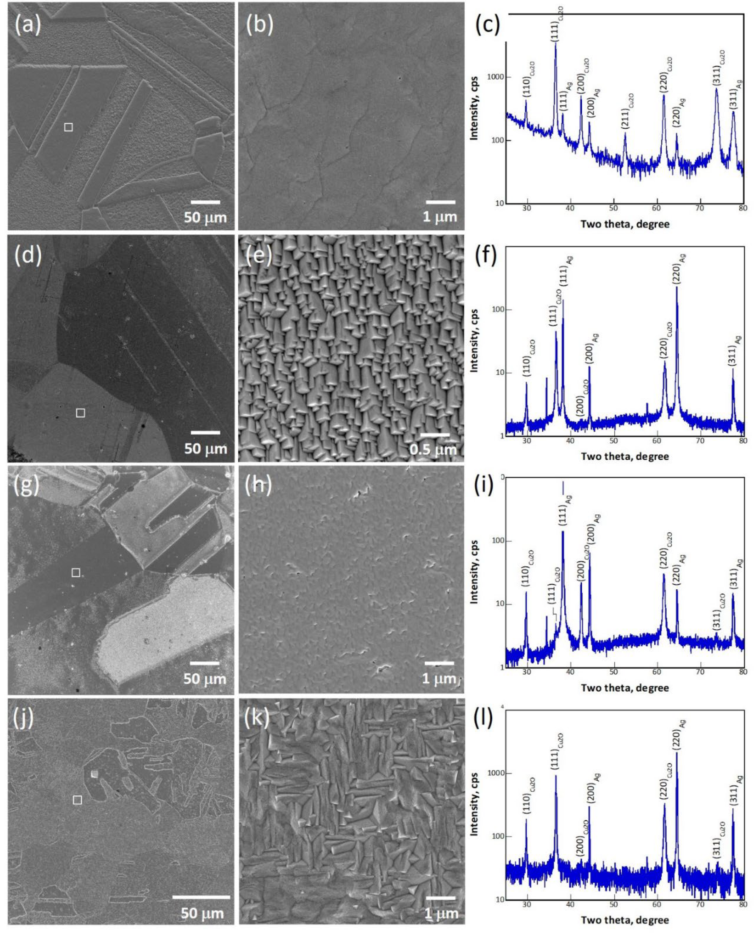
Figure 2.
X-ray analyses for an epitaxial Cu2O film grown on a Cu (111) substrate (sample 111): (a) a ω/2θ scan with an ω scan for the (111)Cu2O peak in the inset (left), and phi scans of (200)Cu and (200)Cu2O peaks with a SEM micrograph in the inset (right).
Figure 2.
X-ray analyses for an epitaxial Cu2O film grown on a Cu (111) substrate (sample 111): (a) a ω/2θ scan with an ω scan for the (111)Cu2O peak in the inset (left), and phi scans of (200)Cu and (200)Cu2O peaks with a SEM micrograph in the inset (right).
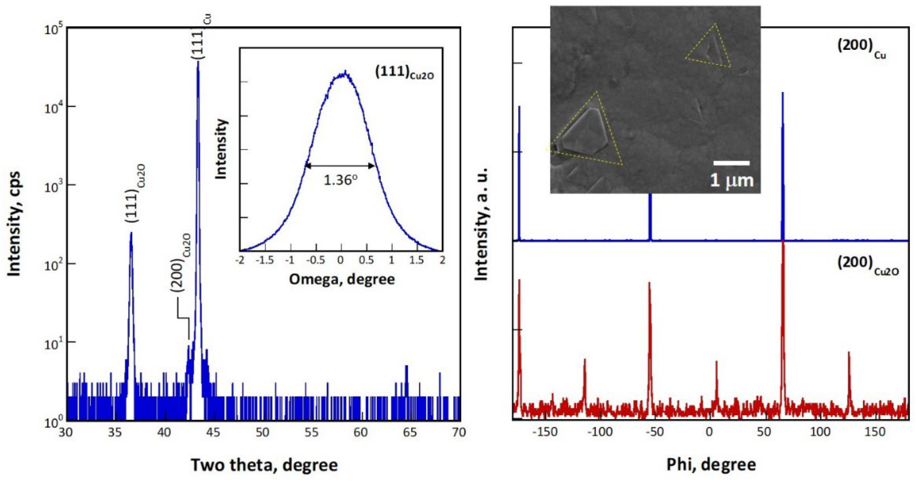
Figure 3.
Absorption spectra of Cu2O samples: single crystals at temperature, shown by legends: (a)—sample SC(111) and (b)—sample SC(100); thin films at RT: (c)—sample 13, (d)—sample 39.
Figure 3.
Absorption spectra of Cu2O samples: single crystals at temperature, shown by legends: (a)—sample SC(111) and (b)—sample SC(100); thin films at RT: (c)—sample 13, (d)—sample 39.
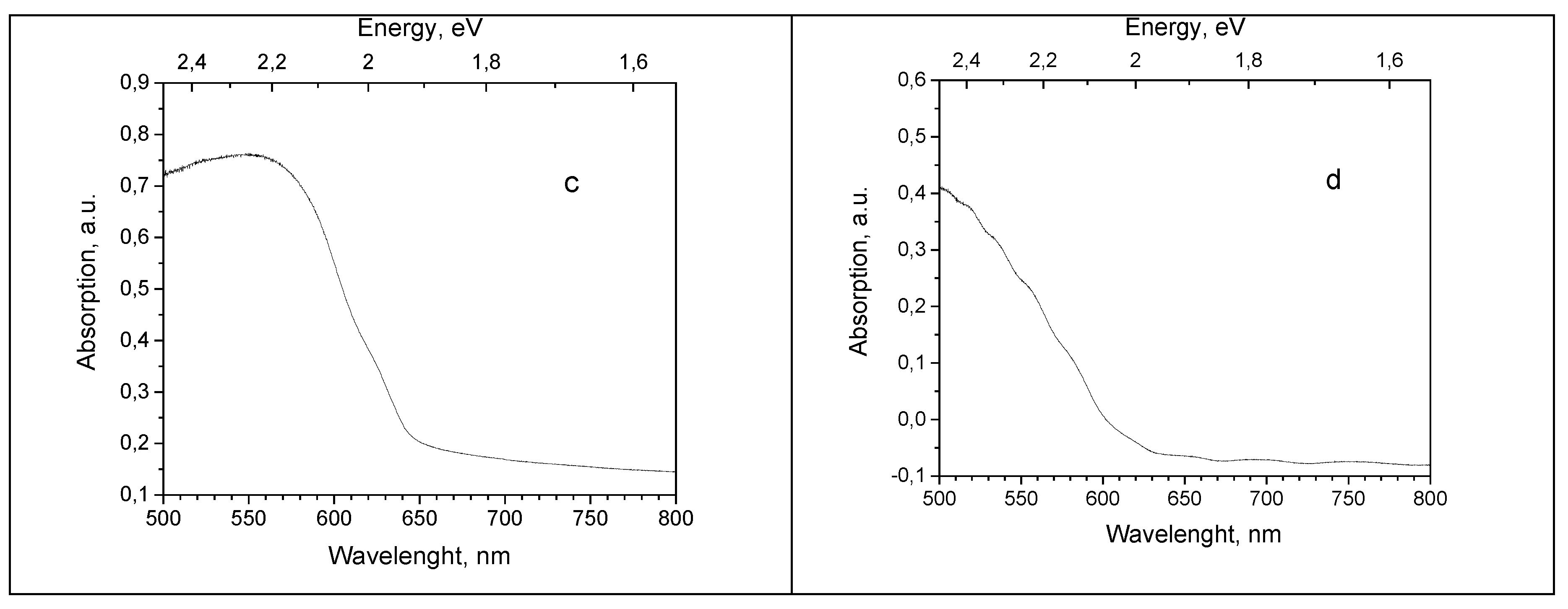
Figure 4.
Photoluminescence of Cu2O single crystals under 532 nm laser excitation at varied temperatures. Sample names, applied laser power and temperatures are shown on graphs.
Figure 4.
Photoluminescence of Cu2O single crystals under 532 nm laser excitation at varied temperatures. Sample names, applied laser power and temperatures are shown on graphs.
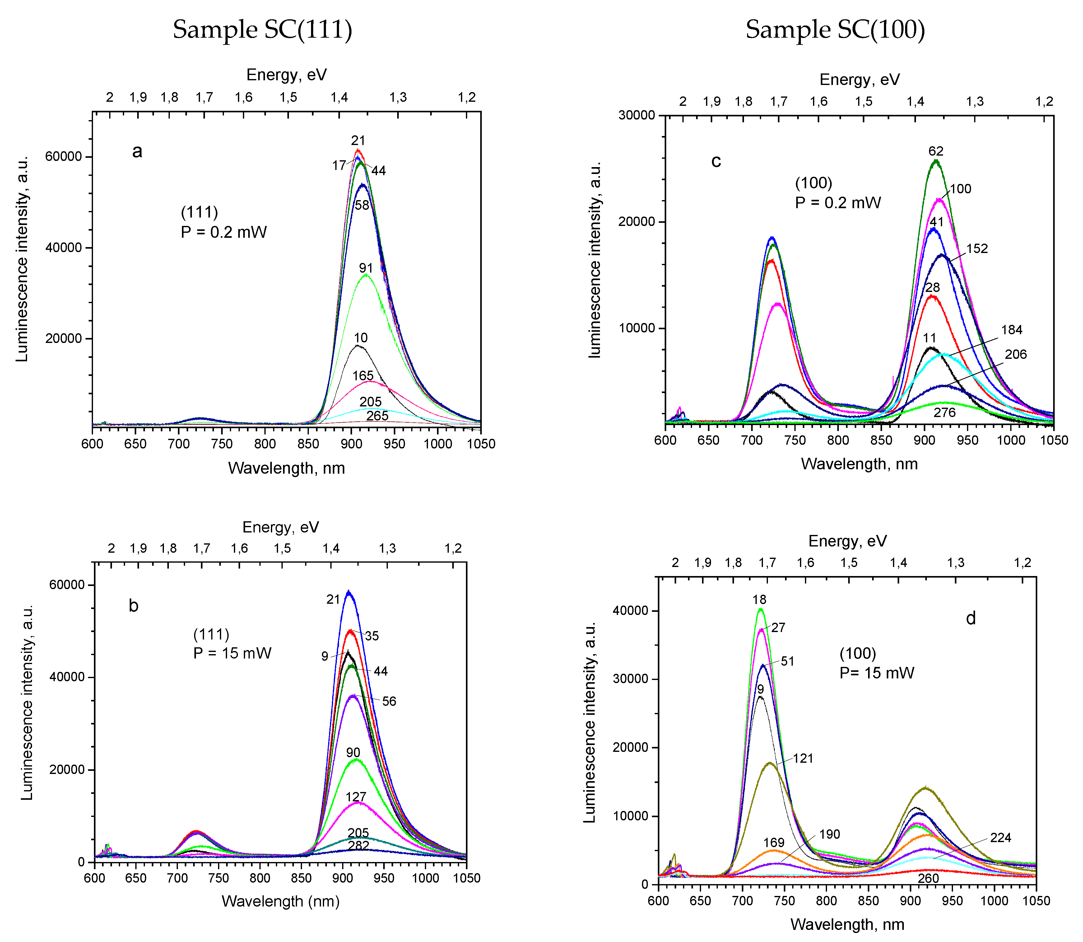
Figure 5.
(a). Thermal dependence of luminescence intensity for sample SC(111) for bands and excitation powers: 1–910 nm, 15 mW; 2–720 nm, 15 mW; 3–910 nm, 0.2 mW; 4–720 nm, 0.2 mW. (b). Arrhenius plot for thermal dependence of luminescence intensity for sample SC(111) for bands and excitation powers: 1–910 nm, 15 mW; 2–720 nm, 15 mW; 3–910 nm, 0.2 mW; 4–720 nm, 0.2 mW.
Figure 5.
(a). Thermal dependence of luminescence intensity for sample SC(111) for bands and excitation powers: 1–910 nm, 15 mW; 2–720 nm, 15 mW; 3–910 nm, 0.2 mW; 4–720 nm, 0.2 mW. (b). Arrhenius plot for thermal dependence of luminescence intensity for sample SC(111) for bands and excitation powers: 1–910 nm, 15 mW; 2–720 nm, 15 mW; 3–910 nm, 0.2 mW; 4–720 nm, 0.2 mW.
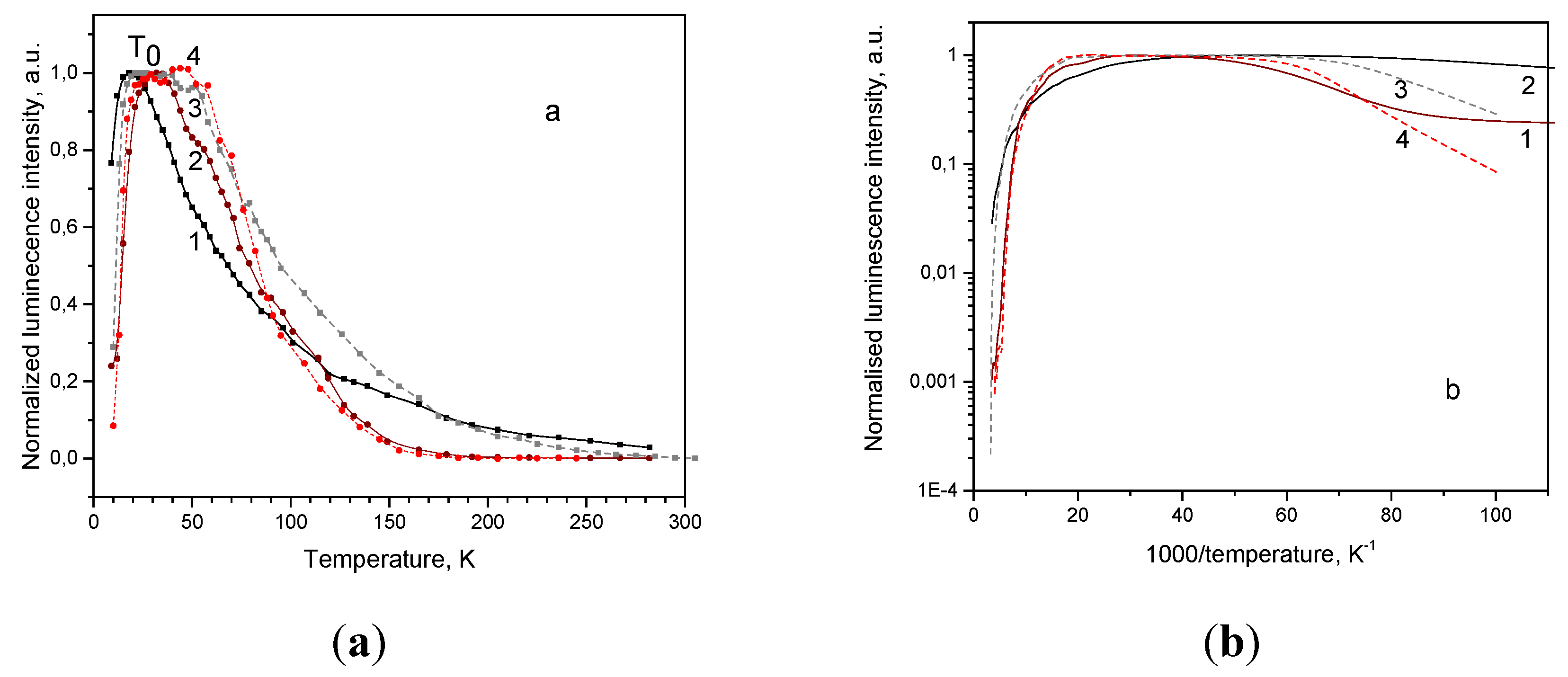
Figure 6.
Normalized photoluminescence spectra of Cu2O samples under excitation with 532 nm laser at 10 K: thin films 1–30, 2–40, 3–13, 4–39, 5–111; and 6–crystalline sample SC(100).
Figure 6.
Normalized photoluminescence spectra of Cu2O samples under excitation with 532 nm laser at 10 K: thin films 1–30, 2–40, 3–13, 4–39, 5–111; and 6–crystalline sample SC(100).
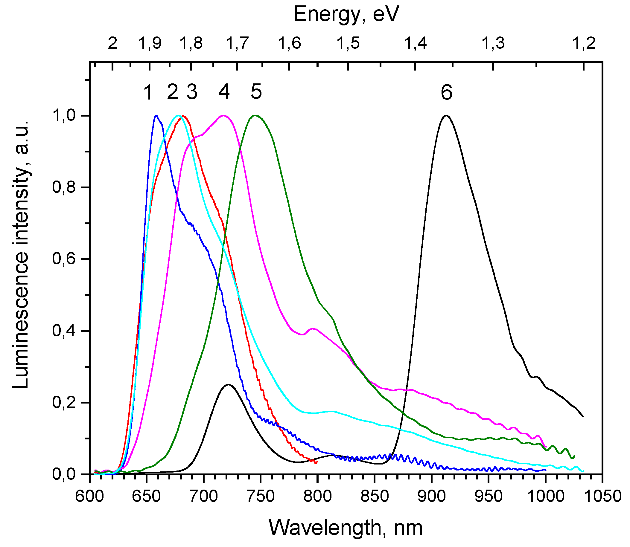
Figure 7.
Spectral properties of Cu2O epilayer on Cu single crystal substrate (sample 111) under 532 nm laser excitation: (a) Thermal evolution of PL spectra; (b) polarized PL spectra at different angular positions of the analyzer at 10 K (angular degrees are shown on the graph).
Figure 7.
Spectral properties of Cu2O epilayer on Cu single crystal substrate (sample 111) under 532 nm laser excitation: (a) Thermal evolution of PL spectra; (b) polarized PL spectra at different angular positions of the analyzer at 10 K (angular degrees are shown on the graph).
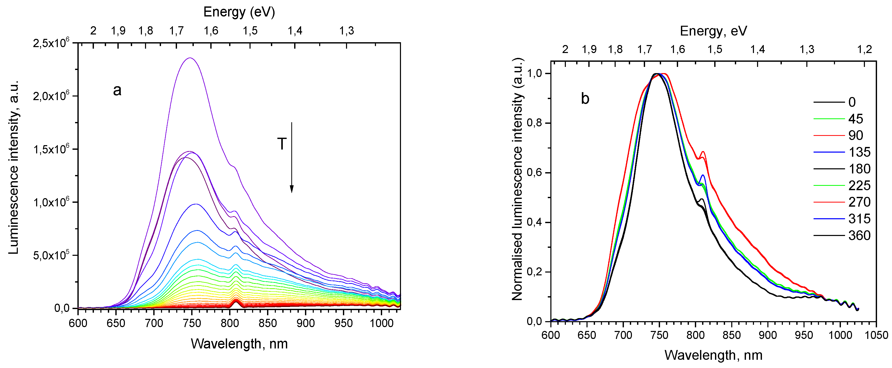
Figure 8.
Thermal evolution of PL subbands for thin film sample 111: (a) PL intensity; (b) Arrhenius plot for the subbands: 1–680 nm, 2–735 nm, 3–820 nm, 4–920 nm.
Figure 8.
Thermal evolution of PL subbands for thin film sample 111: (a) PL intensity; (b) Arrhenius plot for the subbands: 1–680 nm, 2–735 nm, 3–820 nm, 4–920 nm.
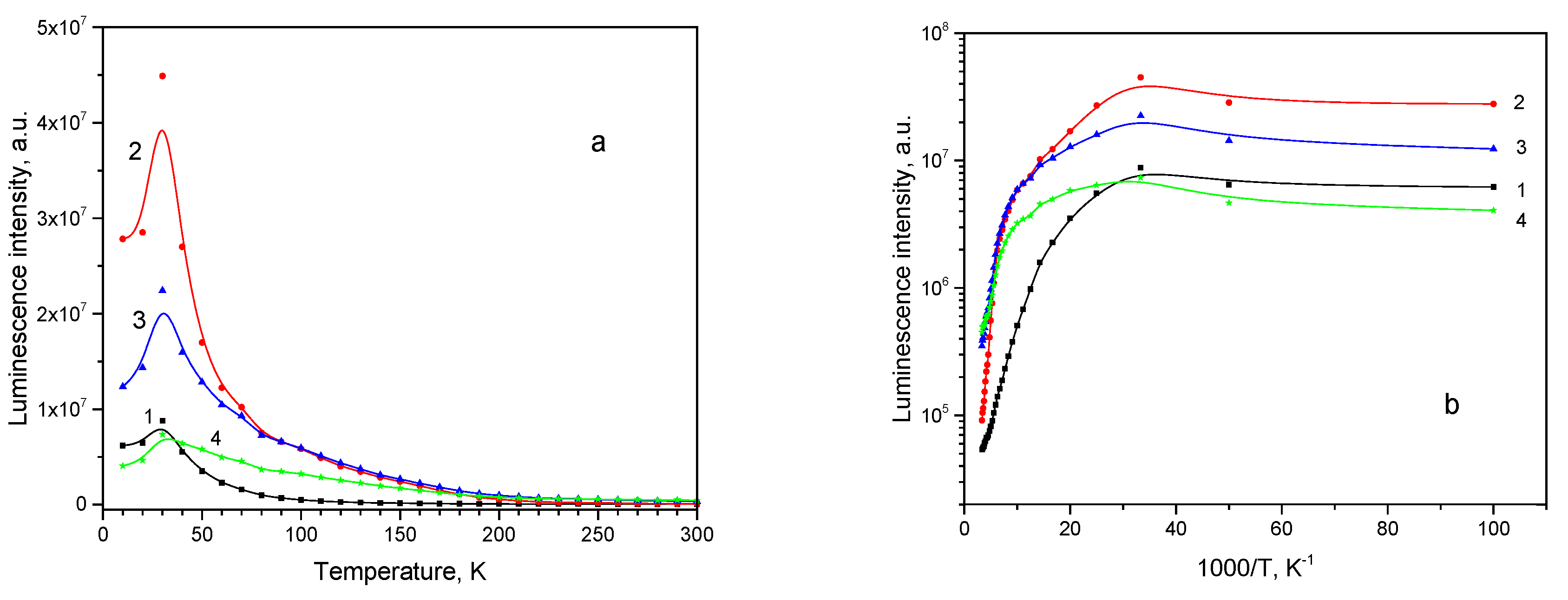
Figure 9.
Spectral properties of Cu2O thin film on Ag polycrystalline substrate (sample 13) under 532 nm laser excitation: (a) Thermal evolution of PL spectra; (b) polarized PL spectra at different angular positions of the analyzer at 10 K (angular degrees are shown on the graph).
Figure 9.
Spectral properties of Cu2O thin film on Ag polycrystalline substrate (sample 13) under 532 nm laser excitation: (a) Thermal evolution of PL spectra; (b) polarized PL spectra at different angular positions of the analyzer at 10 K (angular degrees are shown on the graph).
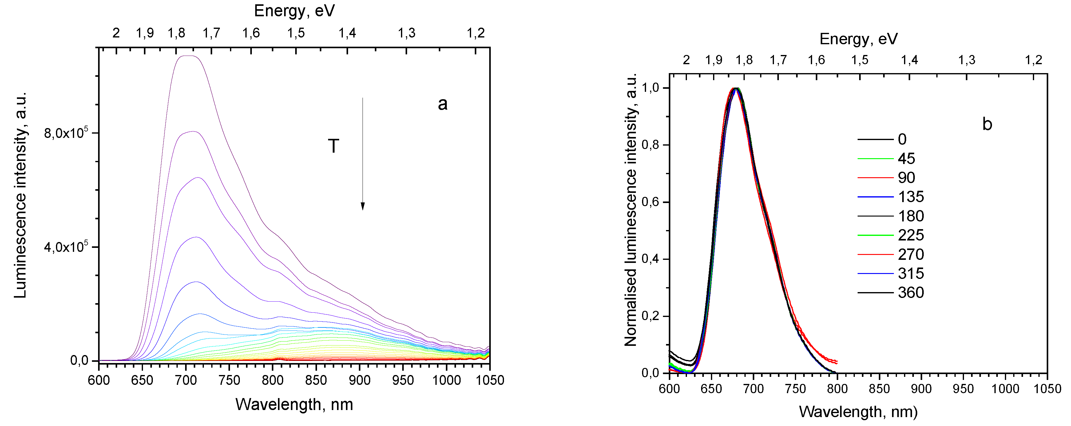
Figure 10.
Thermal evolution of PL subbands for thin film sample 13: (a) PL intensity; (b) Arrhenius plot: 1–680 nm , 2–735 nm, 3–820 nm, 4–920 nm.
Figure 10.
Thermal evolution of PL subbands for thin film sample 13: (a) PL intensity; (b) Arrhenius plot: 1–680 nm , 2–735 nm, 3–820 nm, 4–920 nm.
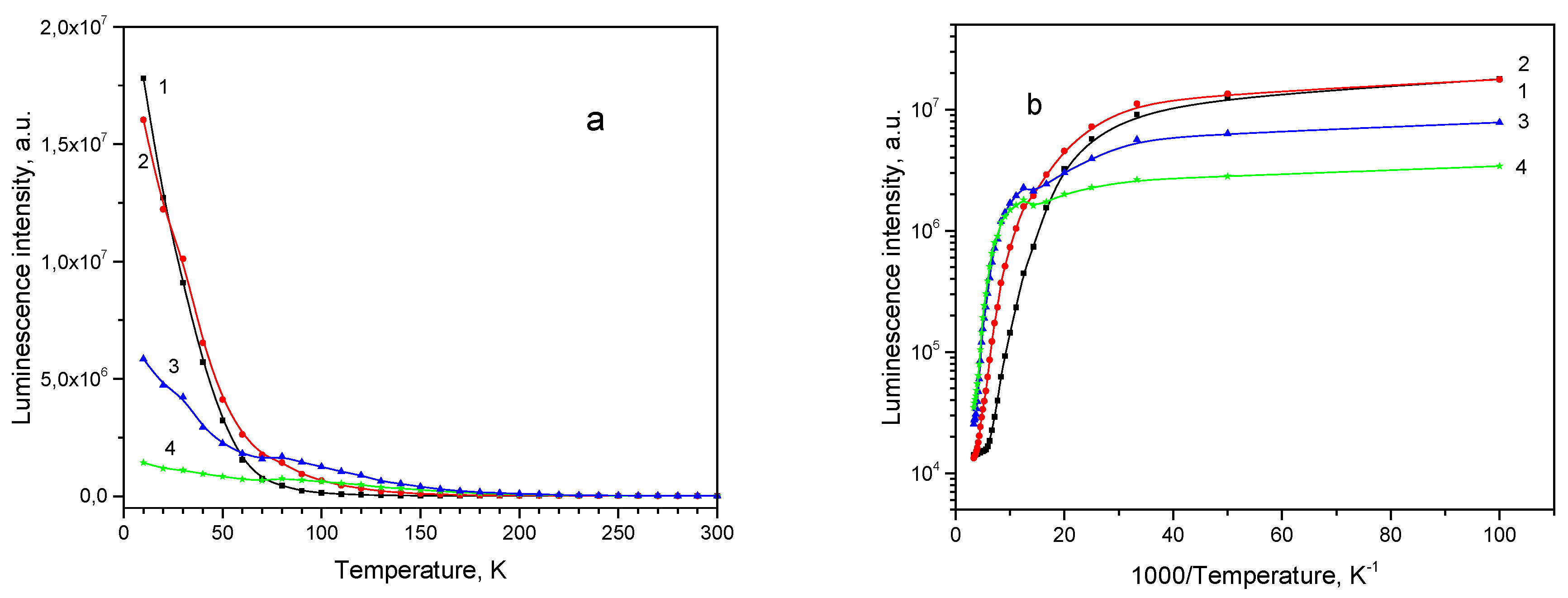
Figure 11.
Spectral properties of Cu2O thin film on Ag polycrystalline substrate (sample 30) under 532 nm laser excitation: (a) Thermal evolution of PL spectra; (b) polarized PL spectra at different angular positions of the analyzer at 10 K (angular degrees are shown on the graph).
Figure 11.
Spectral properties of Cu2O thin film on Ag polycrystalline substrate (sample 30) under 532 nm laser excitation: (a) Thermal evolution of PL spectra; (b) polarized PL spectra at different angular positions of the analyzer at 10 K (angular degrees are shown on the graph).
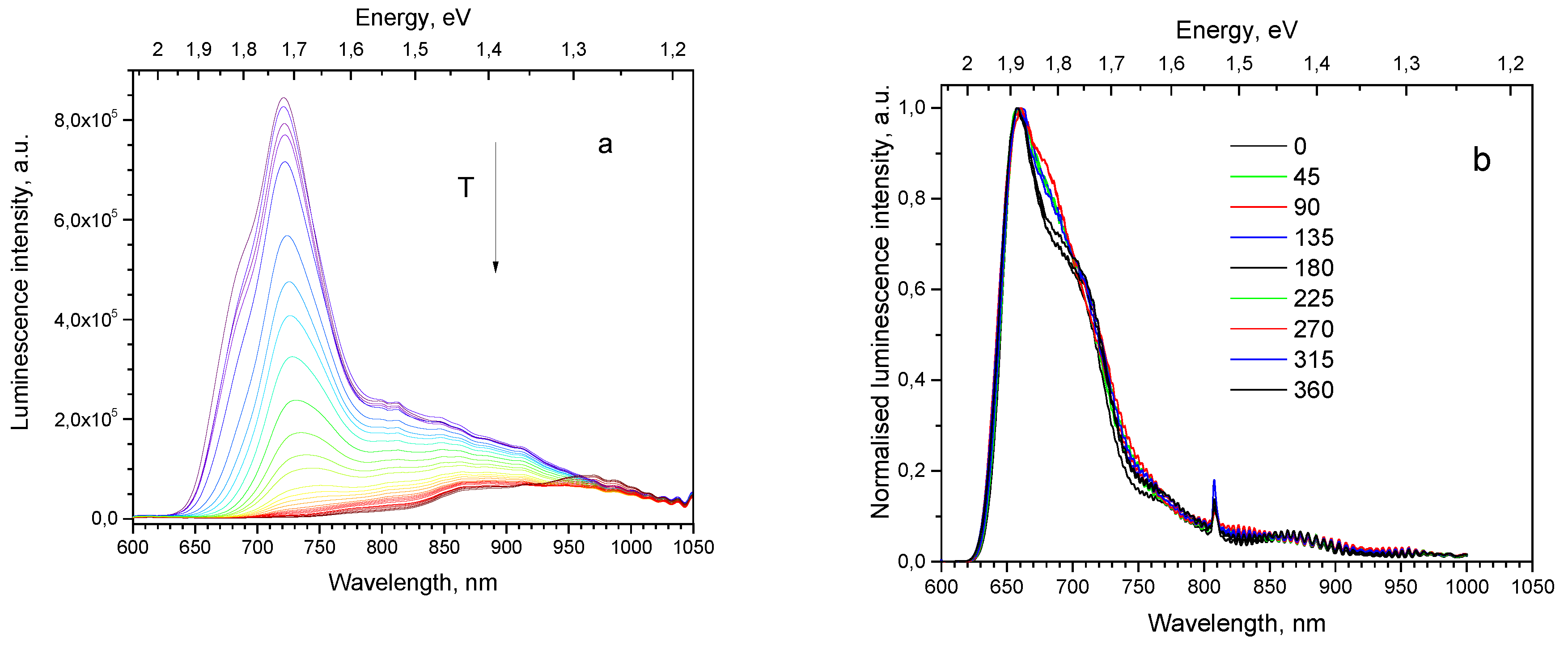
Figure 12.
Thermal evolution of PL subbands for thin film sample 30: (a) PL intensity; (b) Arrhenius plot: 1–680 nm , 2–735 nm, 3–820 nm, 4–920 nm.
Figure 12.
Thermal evolution of PL subbands for thin film sample 30: (a) PL intensity; (b) Arrhenius plot: 1–680 nm , 2–735 nm, 3–820 nm, 4–920 nm.
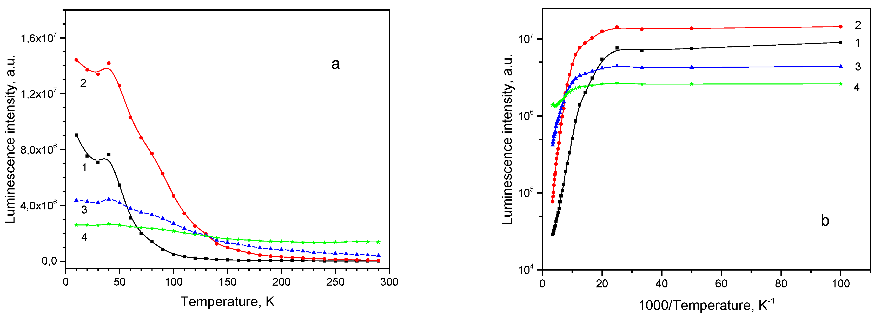

Table 1.
Electrolyte and deposition conditions of the Cu2O thin film samples.
| Sample number | Substrate | Lactic acidconcentration, M | pH | Thickness, m | Current density (G) / Potential (P) |
| 13 | PC Ag | 1.3 | 12 | 8.7 | -0.38 V (P) |
| 30 | PC Ag | 3.0 | 12 | 1.3 | -0.44 V (P) |
| 39 | PC Ag | 3.0 | 9 | 1.3 | -0.15 V (P) |
| 40 | PC Ag | 4.0 | 12 | 1.3 | -0.43 V (P) |
| 111 | (111) Cu | 1.3 | 12 | 1.0 | 0.25 mA/cm2 (G) |
PC: polycrystal.
Table 2.
Texture and crystal habit planes for the four samples.
| Sample | Texture | Facet plane |
| 13 | <111>//ND | {111} |
| 30 | <111>//ND | {100} |
| 39 | <200>//ND + <220>//ND | {111} |
| 40 | <111>//ND + <220>//ND | {100} |
| 111 | <111>//ND | {111} |
Table 3.
Optical band gap values for Cu2O single crystal and thin film samples obtained from absorption measurements.
Table 3.
Optical band gap values for Cu2O single crystal and thin film samples obtained from absorption measurements.
| Sample | Eg, eVSC(100) | Eg, eV SC(111) | Eg, eV# 111 | Eg, eV# 13 | Eg, eV# 30 | Eg, eV# 39 | Eg, eV# 40 | |
| 10 | 2.04 ± 0.02 | 2.04 ± 0.02 | ||||||
| 300 | 1.94 ± 0.02 | 1.92 ± 0.02 | 1.91 ± 0.05 | 1.99 ± 0.05 | 1.92 ± 0.05 | 1.94 ± 0.05 | 1.99 ± 0.05 | |
Table 4.
Activation energies of subbands detected in Cu2O single-crystal samples (obtained with an error ≈ 15 %).
Table 4.
Activation energies of subbands detected in Cu2O single-crystal samples (obtained with an error ≈ 15 %).
| Sample | Ea, eV <B/>660 nm | Ea, eV <B/>680 nm | Ea, eV <B/>720 nm | Ea, eV <B/>810 nm | Ea, eV <B/>920 nm | |
| Cu2O crystal<B/>(orientation)<B/>@ laser irradiation power<B/> | SC(111) <B/> @ 0.2 mW | 80<B/> | 150 | |||
| SC(111) <B/>@ 15 mW | 93<B/> | 190 | ||||
| SC(100) <B/>@ 0.2 mW | 89 | 22 | 135 | |||
| SC(100) <B/>@ 15 mW | 97<B/> | 20 | 197 | |||
| Cu2O thin films, | 111 | 32 | 77 | 42 | 15 + 37 | |
| 13 | 36 | 43 | 62 | 65 | ||
| 30 | 41 | 59 | 33 | 22 | ||
| 39 | 59 | 86 | 37 | 12 + 126 | ||
| 40 | 32 | 40 | 55 | 37 | 18 + 247 | |
Disclaimer/Publisher’s Note: The statements, opinions and data contained in all publications are solely those of the individual author(s) and contributor(s) and not of MDPI and/or the editor(s). MDPI and/or the editor(s) disclaim responsibility for any injury to people or property resulting from any ideas, methods, instructions or products referred to in the content. |
© 2023 by the authors. Licensee MDPI, Basel, Switzerland. This article is an open access article distributed under the terms and conditions of the Creative Commons Attribution (CC BY) license (http://creativecommons.org/licenses/by/4.0/).
Copyright: This open access article is published under a Creative Commons CC BY 4.0 license, which permit the free download, distribution, and reuse, provided that the author and preprint are cited in any reuse.


