
Submitted:
11 February 2023
Posted:
13 February 2023
You are already at the latest version
Abstract
The concentration of data from multiple links to a single output is an essential task performed by High-Energy Physics (HEP) Data Acquisition Systems (DAQs). At high and varying data rates combined with the large width of the concentrator’s output interface, this task is non-trivial. This paper presents a concentrator based on the Beneš network, which provides efficient concentration without using a high-frequency clock internally. It warrants that empty data are eliminated and does not disturb the data time-ordering if the data rates significantly differ between inputs. Additionally, it is well suited to FPGA implementation. It is based on simple data-routing primitives and may be fully pipelined.
Keywords:
FPGA
; DAQ
; Data concentration
; Beneš network
1. Introduction
Most detectors in high-energy physics (HEP) experiments deliver massive data streams in multiple channels. Reception of this data and its delivery to the analyzing computers is the task of the readout chains. In the case of experiments using a trigger, the data must be processed locally to elaborate the level one (L1) trigger decision. Preparing it for concentration may be a side effect of this process. The data is zero suppressed – invalid or empty data words are removed from the stream. Finally, the data is buffered in memory, which may offer the data width conversion. It may be written with single data words and read with multiple words in parallel, as required by the DAQ interface.
In the triggerless readout, the situation is different. The readout system does not need to perform complex local processing of data. Extraction of interesting events is done in further stages of the DAQ (“event builder” and “event filter” [1] or “event selector” [2]). The responsibility of the readout system is different in this configuration. It should almost transparently deliver the detector data to DAQ. For triggerless DAQ, a very popular architecture is the one where the DAQ computers are located near the detectors, and data concentrating boards are the PCIe cards. The PCI Express blocks in FPGA require specific data bus width in the AXI interface. Table 1 shows the available AXI data widths depending on the speed of the link, the width of the PCIe lane, and AXI clock frequency. For PCIe 8xGen3, it is necessary to work with 256-bits wide data.
The detector data generated by the particle detection is usually short. For example, for the STS-XYTER (also known as SMX) [3]) the data is 24-bit long. In the concentrated stream, the data must be accompanied by metadata describing its origin, resulting in a final size of 32 bits. Hence, the data concentrator must efficiently pack 32-bit detector data into 256-bit PCIe data.
The problem may be generalized as described in the next section.
1.1. Formulation of the Problem
The system receives the data words from N inputs at frequency , and puts them into the records able to store M words, which are read at frequency. The system has sufficient bandwidth. The following condition is met:
The intensity of the data stream delivered by the inputs may be different and may vary in time. It means that some links may deliver invalid (or empty) data in a particular period of the input clock. Those invalid data should be skipped not creating “holes” in the output stream. For event reconstruction in the triggerless DAQ, the data must be assigned to a particular time period1. Therefore, an essential requirement is that the concentrator disturbs the time-ordering of the input data as little as possible.
In the next chapter, the existing solutions to the concentration problem are presented, and their disadvantages are discussed.
2. Existing Solutions for Concentrators
Unfortunately, finding published information about the data concentration methods used in existing FPGA-based data concentrators is difficult. The presented review is based on seldom publications and presentations, publicly available source code analysis, or the authors’ experience.
Most existing solutions may be grouped into two categories described in the following sections.
2.1. High Speed Polling
The trivial solution is based on browsing all inputs at the frequency (see Figure 1).
If valid data is found, it is copied to the asymmetric FIFO queue with an input width of 1 word and an output width of M words. That warrants that no valid data is skipped, and the output words are filled with valid data only. The only problem with that solution is that the necessary may be too high to be acceptable for FIFO in FPGA. Therefore this method may be used only in case of low input clock frequency or concentrating data from a small number of inputs.
This solution is used for concentrating the data from STS-XYTER2 [3] front-end ASICs transmitted through GBT Links [4] in the readout chain of the STS detector in the CBM experiment [5]. In that readout, each GBT Link transports data from 14 E-Links working with a 320 Mb/s rate. The 8b/10b encoded hit data occupy 30 bits in the E-Link. Therefore, the hit data rate in the individual E-Link is not higher than . That is a low frequency. Because , the data can be safely concentrated by consecutive scanning all 14 E-Link outputs at 160 MHz.
Another example is the firmware for the CRU board [6] used by the ALICE experiment at LHC at CERN. It uses a round-robin scanning of the output of FEE links (see [6], Figure 8). Then only the valid data are packed into the 256-bit wide FIFO, delivering the data to PCIe. The authors do not describe at which frequency the inputs are scanned.
2.2. Width Conversion in Input Channels
A high-speed scanning may be avoided if width conversion is performed in the input channels. In this solution, the small FIFOs with one-word wide input and M-words wide output are placed in each input channel, as shown in Figure 2. This solution does not require using a very high clock frequency. However, it has other disadvantages. If the link occupancy significantly differs between inputs, the concentration may significantly change the time-ordering of data. The data from low-rate links may get significantly delayed until M data words are collected. That problem may be solved by introducing the timeout, after which the non-empty FIFO outputs its content even if it contains less than M words. However, that modification results in inserting “holes” into the concentrated stream. Another disadvantage is the necessity to use a separate width-converting FIFO in each input channel. Those FIFOs may have limited depth, enabling implementation based on distributed RAM, but they may still increase resource consumption. Finally, that solution cannot use a simple counter-driven multiplexer periodically browsing the data. That solution requires a more complex data-driven multiplexer, which automatically selects the first input providing the complete data record after the previously serviced one (i.e., it implements the round-robin policy).
This approach seems to be used in the firmware for the FELIX board in the ATLAS experiment readout at CERN [7]. Unfortunately, the operation of the data concentrator in the FELIX firmware is not described in detail in any paper. However, the sources of that firmware are publicly available, enabling analysis of the concentrator code. The concentration is done in the CRToHostdm module [8] containing the asymmetric FIFO responsible for concatenating a few words and width conversion. Outputs of FIFOs from multiple channels are scanned in the CRToHost module [9].
2.3. Need for Another Concentration Method
None of the above methods matches all the requirements described in Section 1.1. Therefore, a new method is proposed in the next section.
3. Proposed Solution—Concentration with the Direct Routing of Data
It is possible to avoid the disadvantages of the previously described solutions by directly routing data from inputs to the proper position of the output record. Such a solution is shown in Figure 3. The key functionality needed in this method is a capability to write the data from each individual input to a selected position in the output record. A dedicated controller calculates the desired location of data from each input. The controller must keep track of the occupancy of the output data. Additionally, it receives the “valid” flags from the input words. The controller starts with an output record occupancy equal to zero. If, for example, it receives valid words in three inputs, it routes them to positions 0, 1, and 2 in the output record and changes the occupancy to 3. The next valid word will be routed to position 4, and so on. When the output record is filled, the output strobe is generated, the collected words are transferred to the output FIFO, and the occupancy is set to 0.
There is, however, a problem if the concentrator receives more valid data than needed to fill the output record. Those superfluous words must be stored somewhere. For that purpose, an “auxiliary record” register is introduced. The controller generates a write strobe for both registers. The output strobe causes the transfer of the output record to FIFO and, at the same time, of the auxiliary record to the output record. The modified concentrator is shown in Figure 4.
The presented concentrator should work correctly, but its implementation in FPGA is inefficient. Implementing M multiplexers routing the data words consumes many resources and generates long critical paths in the FPGA. Therefore yet another modification is needed. The multiplexers must be replaced with more efficient blocks for routing the data.
3.1. Concentrator Based on Beneš Network
A similar problem had to be solved in telecommunication networks for routing connections. Networks enabling arbitrary data permutation between their inputs and outputs are known as Beneš networks and have been described in [10]. An example of such network routing 8 inputs to 8 outputs is shown in Figure 5. The Beneš network uses simple switches with two inputs and two outputs, transmitting the data transparently or swapping them. They may be efficiently implemented in FPGA. The lengths of all data paths are the same, so this network can be efficiently pipelined, which results in a short critical path. The general scheme of the concentrator based on the Beneš network is shown in Figure 6.
The problem with the Beneš network is that its complexity quickly grows when the number of inputs and outputs increases. For example, the 4x4 Beneš network requires 6 switches in 3 layers, the 8x8 Beneš network – 20 switches in 5 layers, the 16x16 Beneš network – 56 switches in 7 layers. Generally, for inputs and outputs, the network requires switches in layers.
Additionally, finding the configuration of switches that provides the required data routing is a complex task [11]. For small networks, it is possible to use a “brute force” approach to check all possible configurations and create a table with configurations needed for all possible routings. For an 8x8 network, it is necessary to analyze possibilities, and find the right configuration for possible permutations. For a 16x16 network, the number of possible switch configurations is , and the number of possible permutations is . Therefore, neither analysis of all possible configurations nor storing the right configuration for each possible permutation is viable. Therefore, an 8x8 network is used as a basis for the concentrator with the structure shown in Figure 7.
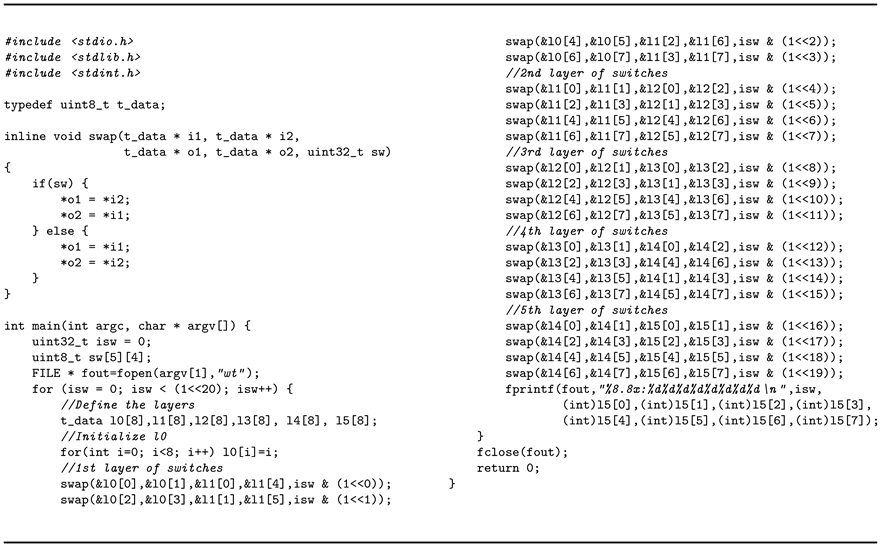
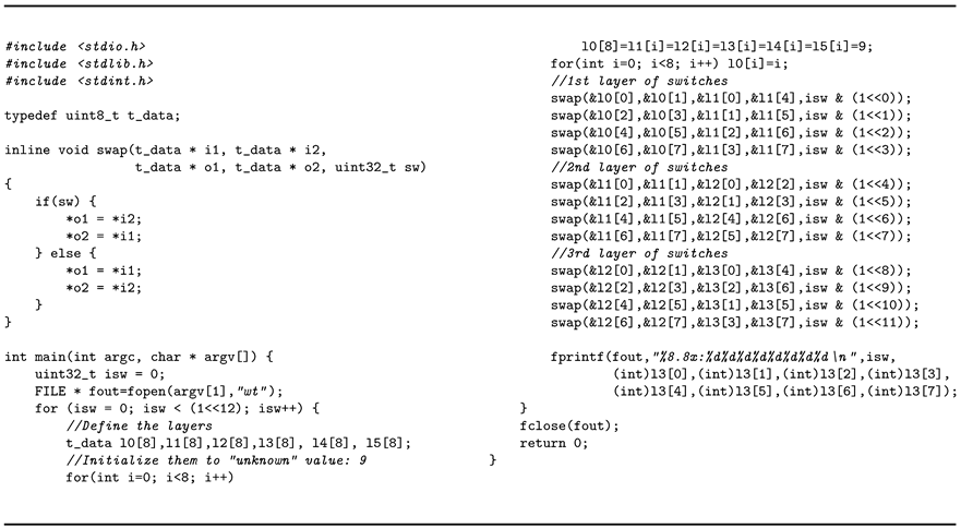
A simple C utility was written to investigate the switch settings providing different data permutations, as shown in Listing 1. It generates a simple file with lines containing the value of the switch configuration word and the data permutation it generates. This generated file is then read by the Python utility, which creates a dictionary where the key is the particular permutation, and the value is the smallest value of the switch configuration word that provides it. Of course, not all possible permutations are needed in the concentrator. What is needed is routing the valid input words to the auxiliary or output record, starting from the first free output position, and preserving their order. Therefore, the Python utility iterates over all possible occupancies of the output record, and all possible combinations of the input data valid flags and finds the corresponding switch configuration. The analysis of the generated dictionary resulted in an interesting finding. The switch configuration values generating all needed permutations are always below 0x400. It means that only the lowest 11 bits are used. The switches in layers 3 to 5 are never used. That means that the Beneš network may be significantly reduced for that particular application using a limited set of permutations, as shown in Figure 8. Of course, that also resulted in a reduction of the C utility (see Listing 2).
3.2. Calculation of the Future Occupancy
The concentrator controller is also responsible for the calculation of the future occupancy of the output record. That value is needed in the next clock period. Therefore, its calculation is separated from finding the switch configuration. The switch configuration values may be stored in a BRAM-based look-up table. Adding pipeline registers before the Beneš network may compensate for the resulting delay. That’s not possible in case of future occupancy. That must be calculated in combinational logic. The implementation used in the project is shown in Listing 3.
 |
| Listing 1. C model of the 8x8 Beneš network |
 |
| Listing 2. C model of the reduced 8x8 Beneš network |
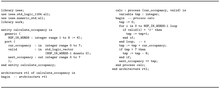 |
| Listing 3. VHDL implementation of the combinational function calculating the future output record occupancy from the current one and the vector of valid input flags. |
4. Practical Implementations of the Concentrator
Beneš-network-based concentrator appeared to be useful in different data acquisition systems currently developped. The design may be adjusted to particular needs, as shown in this section.
The solution based on 8x8 Beneš networks is needed for the GERI board [12] based on Trenz TEC0330 PCIe card [13]. This board, when supplemented with an FMC card with 8 SFP+ cages (e.g., [14]), enables concentration of data from 8 GBT Links to the DMA system [15] connected to the 8xGen 3 PCIe bus. The DMA system uses 256-bit data which may be treated as a record containing eight 32-bit words. Thence, the solution described in the previous section may be directly applied.
If the GERI board is connected to the TFC system [16], one SFP+ cage is used for the TFC communication. In that case, a smaller 7x8 Beneš network is needed. It may be obtained from an 8x8 network. The 7th input should be connected to both inputs in the last switch in layer 0. That eliminates a need to control that switch. Its control input may be connected to a constant value. As a result, the number of switches to be controlled is reduced from 12 to 11. That configuration is shown in Figure 9.
Special solutions are needed when it is necessary to concentrate data from more than eight inputs. Such a situation occurred in designing the firmware for the new CRI2 [17] readout board for CBM [18] experiment. Currently planned hardware solutions need to concentrate data either from 9 or 12 GBT Links delivering data at 160 MHz to a 256-bit wide word at a frequency up to 250 MHz. Of course, using the Beneš network with a size limited to 8x8 requires time multiplexing the input data. However, it does not require as high frequency as the high-speed polling method described in Section 2.1. For those designs, a dedicated data converter has been developed, which receives two input data sets at frequency , combines them, and then outputs them as three smaller sets at the frequency . In the described system the Beneš network works at a frequency of 240 MHz, which is below 250 MHz.
5. Tests and Results
All five described variants of concentrators have been tested in simulations. The input data were generated as 32-bit words containing consecutive numbers starting from 0x100. The user could set probability that the data word is delivered to the individual input. The tests were performed for various values of probability: very low (0.01), low (0.1), medium (0.5), high (0.9), and very high (1.0). For all tested values of the probability, all five configurations of the concentrator worked correctly. All data delivered to the inputs were transmitted exactly once, and no invalid data were inserted into the output records. The waveforms from a simulation of a 7-inputs concentrator at probability 0.5 is shown in Figure 12.
The most complex configuration with 12 inputs has also been verified in hardware. The implementation was performed in two boards:
For testing in hardware, a special testbench has been prepared with the structure shown in Figure 13. The input data for the concentrator are written via PCIe to the FIFO with asymmetric port width2. Similarly, the output from the concentrator is written to the second FIFO with 256-bit wide input and 32-bit wide output connected to another PCIe-accessible register. Additional control and status registers support resetting the FIFOs and the concentrator, starting the data transfer, and reading the status of both FIFOs.
The design was successfully compiled for both selected platforms. Timing closure was obtained for 160 MHz and 240 MHz frequencies. The resulting resource consumption is shown in Table 2.
The FPGA configured with the testbench FIFO is controlled with the uio_pci_generic driver and a simple Python script. The script resets the FIFOs and the concentrator. Then prepares the input data sets and writes them to the first FIFO. Afterward, it starts the data transfer. Finally, it reads the concentrated data from the second FIFO. For automated tests, the input data sets are prepared similarly to the simulations. The data words containing consecutive values were written to the consecutive inputs. With the probability defined by the user, each input could be skipped.
The tests were repeated multiple times with different probabilities of skipping the input and a different number of input data sets (of course, always smaller than the capacity of the input FIFO). In all tests, the concentrated data were correctly delivered to the output FIFO without losses or duplications.
6. Discussion and Conclusions
The novelty presented concentration method eliminates the disadvantages previous solutions. It does not require scanning inputs at high clock frequency as the high-frequency polling method (see Section 2.1). It does not require multiple width-converting FIFOs, does not inject empty data into the output stream, and does not disturb data time-ordering as the width conversion in the input channels (see Section 2.2).
The proposed method is well-suited for FPGA implementation. The Beneš network used to route the data consists of simple blocks (2x2 switches). No complex multiplexers are needed. Pipeline registers may be added inside the switches, resulting in short critical paths and high maximum clock frequency.
The Beneš network is quite old technology, but the paper describes its usage in a new application area. Additionally, it presents a method that significantly reduced the network size and simplified its configuration due to using the precalculated switches configurations.
The solution is based on an 8x8 Beneš network, but extending it for more inputs is described and tested.
The presented solution may improve the concentration of data, especially in concentrators for triggerless DAQs where a high-speed concentration of non-continuous data streams is needed.
The design is open-source and may be freely reused. The sources are available in repository [20].
Author Contributions
Conceptualization, W.M.Z. and B.M.Z.; software, W.M.Z. and M.G.; validation M.G.; investigation, M.K.; writing—original draft preparation, W.M.Z.; writing–review and editing, all authors; supervision, W.M.Z.; Specific technical contribution of the autors: General concept of the solution, software simulations, W.M.Z.; Concept of using the Beneš network for data routing in concentrator, B.M.Z.; Implementation in HDL, simulations, and testing in hardware M.G.; Review of previous art, M.K.; The percentage contribution of the authors is: M.G.—40%, W.M.Z. – 35%, M.K. – 10% and B.M.Z. – 15%. All authors have read and agreed to the published version of the manuscript.
Funding
This research was partially supported by the statutory funds of Institute of Electronic Systems. This project has also received funding from the European Union’s Horizon 2020 research and innovation programme under grant agreement No 871072.
Conflicts of Interest
The authors declare no conflict of interest.
References
- Colombo, T.; Amihalachioaei, A.; Arnaud, K.; Alessio, F.; Brarda, L.; Cachemiche, J.P.; Cámpora, D.; Cap, S.; Cardoso, L.; Cindolo, F.; et al. The LHCb Online system in 2020: Trigger-free read-out with (almost exclusively) off-the-shelf hardware. J. Physics: Conf. Ser. 2018, 1085, 032041. [Google Scholar] [CrossRef]
- Cuveland, J.d.; Lindenstruth, V.; the CBM Collaboration. A First-level Event Selector for the CBM Experiment at FAIR. J. Physics: Conf. Ser. 2011, 331, 022006. [Google Scholar] [CrossRef]
- Kasinski, K.; Szczygiel, R.; Zabolotny, W.; Lehnert, J.; Schmidt, C.; Müller, W. A protocol for hit and control synchronous transfer for the front-end electronics at the CBM experiment. Nuclear Instruments and Methods in Physics Research Section A: Accelerators, Spectrometers, Detectors and Associated Equipment 2016, 835, 66–73. [Google Scholar] [CrossRef]
- Lehnert, J.; Byszuk, A.; Emschermann, D.; Kasinski, K.; Müller, W.; Schmidt, C.; Szczygiel, R.; Zabolotny, W. GBT based readout in the CBM experiment. J. Instrum. 2017, 12, C02061–C02061. [Google Scholar] [CrossRef]
- Technical Design Report for the CBM Online Systems – Part I. In review.
- Bourrion, O.; Bouvier, J.; Costa, F.; Dávid, E.; Imrek, J.; Nguyen, T.; Mukherjee, S. Versatile firmware for the Common Readout Unit (CRU) of the ALICE experiment at the LHC. J. Instrum. 2021, 16, P05019. [Google Scholar] [CrossRef]
- Wu, W. FELIX: The New Detector Interface for the ATLAS Experiment. IEEE Trans. Nucl. Sci. 2019, 66, 986–992. [Google Scholar] [CrossRef]
- FELIX Firmware Sources—CRToHostdm Module. Available online: https://gitlab.cern.ch/atlas-tdaq- felix/firmware/-/blob/phase2/master/sources/CRToHost/CRToHostdm.vhd (accessed on 25 January 2023).
- FELIX Firmware Sources—CRToHost Module. Available online: https://gitlab.cern.ch/atlas-tdaq-felix/ firmware/-/blob/phase2/master/sources/CRToHost/CRToHost.vhd (accessed on 25 January 2023).
- Mathematical Theory of Connecting Networks and Telephone Traffic (Mathematics in science and engineering ; v. 17); Elsevier, 1965.
- Nikolaidis, D.; Groumas, P.; Kouloumentas, C.; Avramopoulos, H. Novel Benes Network Routing Algorithm and Hardware Implementation. Technologies 2022, 10, 16. [Google Scholar] [CrossRef]
- Dementev, D.; Guminski, M.; Kovalev, I.; Kruszewski, M.; Kudryashov, I.; Kurganov, A.; Miedzik, P.; Murin, Y.; Pozniak, K.; Schmidt, C.J.; Shitenkow, M.; Voronin, A.G.; Zabolotny, W.M. Fast Data-Driven Readout System for the Wide Aperture Silicon Tracking System of the BM@N Experiment. Phys. Part. Nucl. 2021, 52, 830–834. [Google Scholar] [CrossRef]
- TEC0330—PCIe FMC Carrier with Xilinx Virtex-7 FPGA. Available online: https://shop.trenz-electronic.de/en/Products/Trenz-Electronic/PCIe-FMC-Carrier/TEC0330-Xilinx-Virtex-7/ (accessed on 6 January 2023).
- FMC—Octal SFP/SFP+. Available online: https://www.fastertechnology.com/store/fmc-modules/fm-s18.html. (accessed on 6 January 2023).
- Zabołotny, W.M. Versatile DMA Engine for High-Energy Physics Data Acquisition Implemented with High-Level Synthesis, 2023. [CrossRef]
- Sidorenko, V.; Fröhlich, I.; Müller, W.; Emschermann, D.; Bähr, S.; Sturm, C.; Becker, J. Prototype design of a timing and fast control system in the CBM experiment. J. Instrum. 2022, 17, C05008. [Google Scholar] [CrossRef]
- The Readout System of the CBM Experiment. Available online: https://indico.phy.ornl.gov/event/ 112/contributions/566/attachments/492/1342/20211208_169_sro9_cbm_daq_v02.
- Compressed Baryonic Matter Experiment at FAIR. Available online: https://www.cbm.gsi.de/ (accessed on 31 January 2023).
- Xilinx Kintex UltraScale FPGA KCU105 Evaluation Kit. Available online: https://www.xilinx.com/ products/boards-and-kits/kcu105.html. (accessed on 6 January 2023).
- Beneš-Network-Based Concentrator for Triggerless DAQ Systems—Git Repository. Available online: https://gitlab.com/WZabISE/concentrator. (accessed on 31 January 2023).
| 1 | Of course, certain tolerance is unavoidable. Thence, some overlap between consecutive analysis periods is used. |
| 2 | For 12 32-bit wide inputs the necessary width of FIFO is 384 bits for data and 12 for valid flags, resulting in 396 bits. The Xilinx FIFO generator does not support that width. Therefore, a FIFO with 512-bit wide output was used. However, the minimal input width for such a FIFO is 64-bits. Therefore, the input value for that FIFO is concatenated from two PCIe-accessible registers. Writing one of them activates the FIFO write strobe. |
Figure 1.
Structure of the concentrator based on high-speed polling. The central area must work with clock frequency , which may be too high for FPGA.
Figure 1.
Structure of the concentrator based on high-speed polling. The central area must work with clock frequency , which may be too high for FPGA.
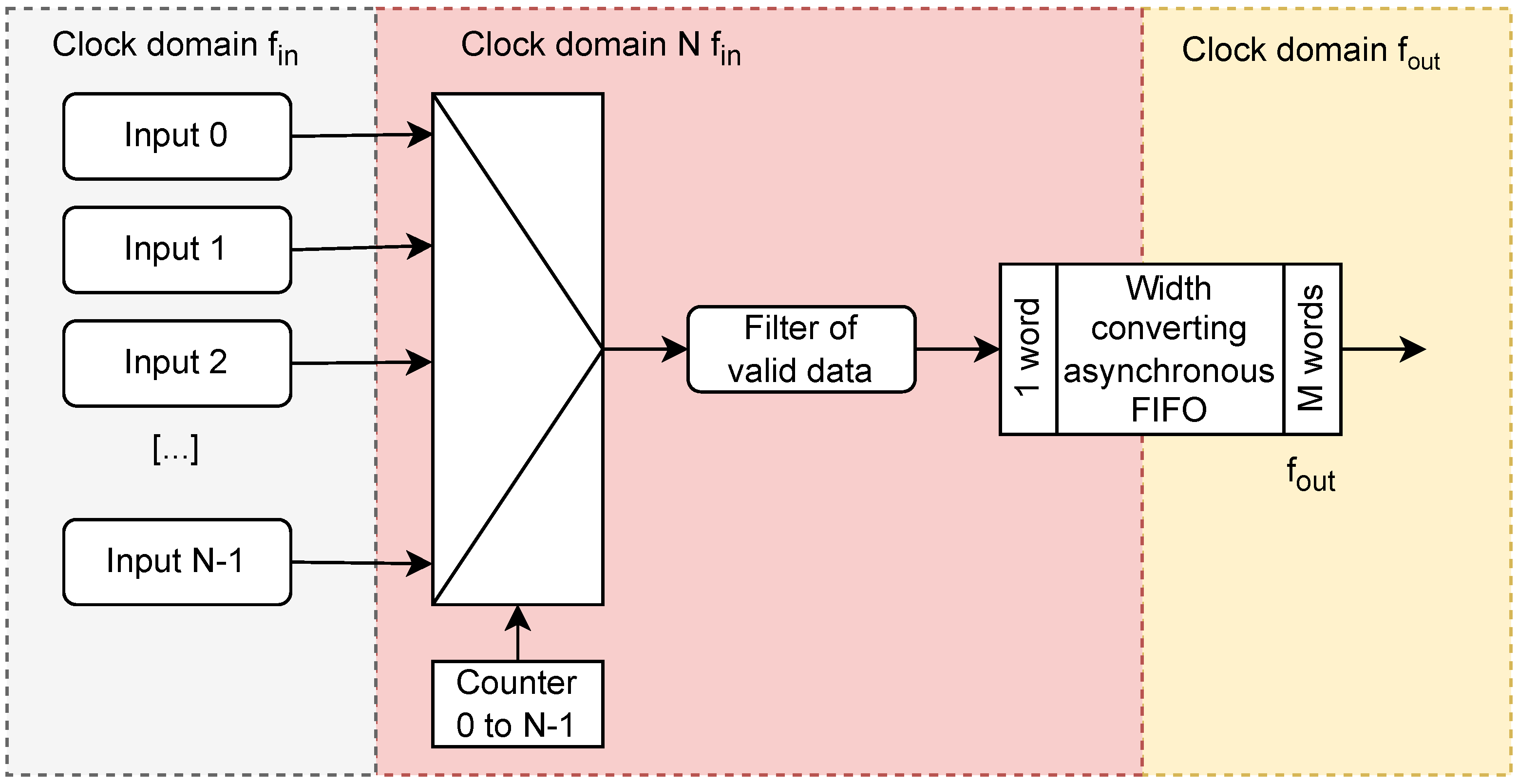
Figure 2.
Structure of the concentrator with width conversion in each input link.
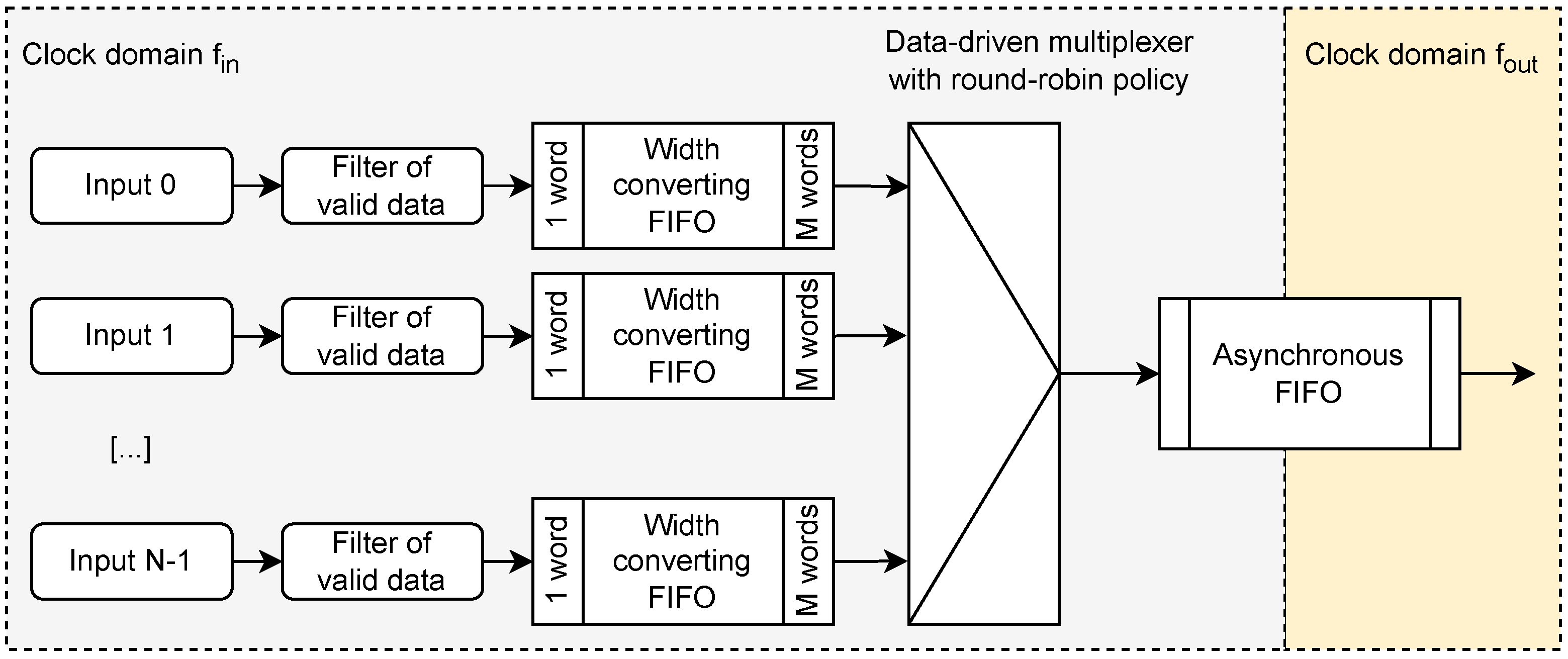
Figure 3.
Structure of the concentrator with the direct routing of data. The controller keeps track of the current output record occupancy and routes each valid input word to the right position in the output record. When the word is completely filled, the output strobe is generated.
Figure 3.
Structure of the concentrator with the direct routing of data. The controller keeps track of the current output record occupancy and routes each valid input word to the right position in the output record. When the word is completely filled, the output strobe is generated.
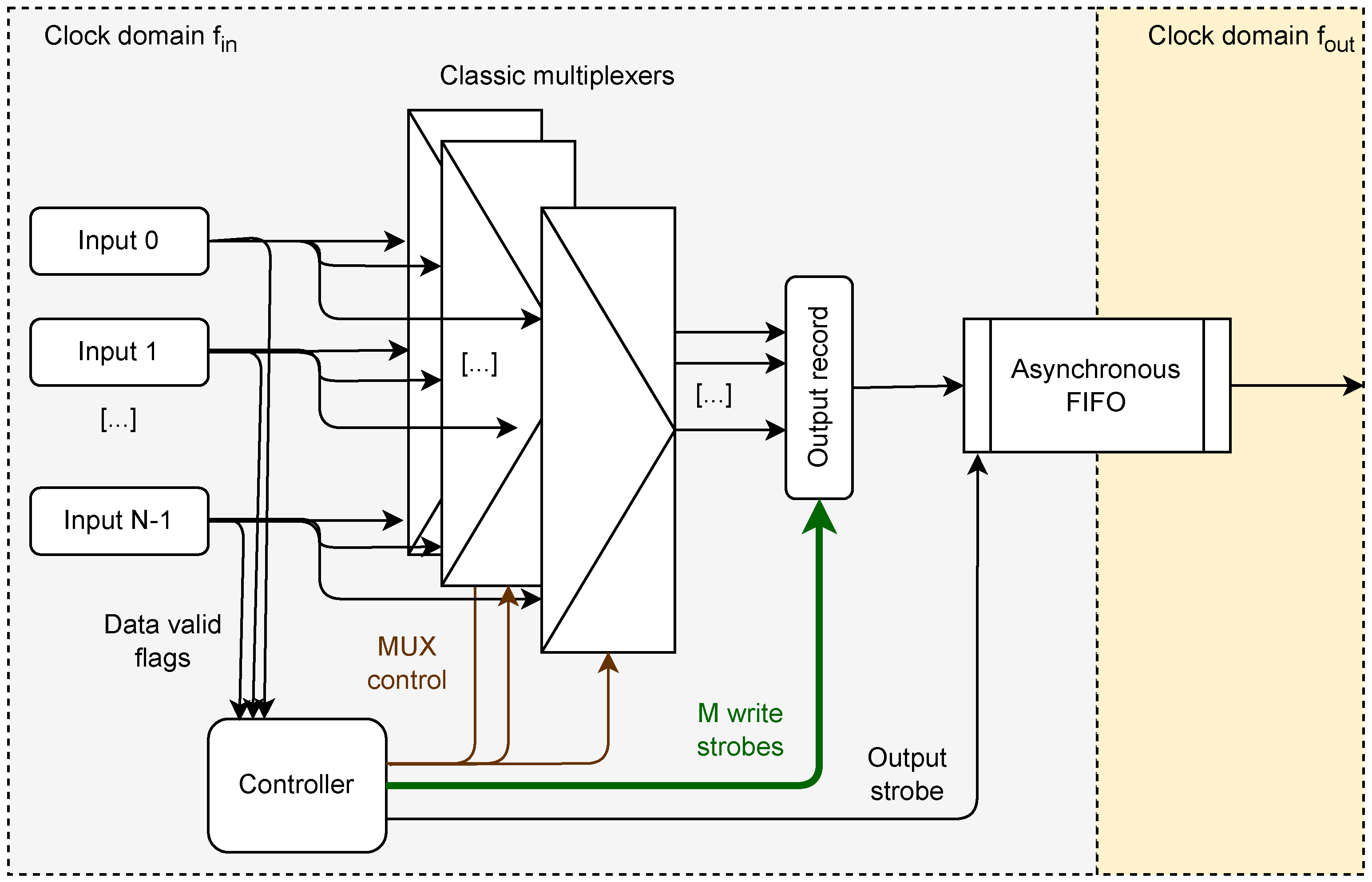
Figure 4.
Structure of the concentrator with the direct routing of data and added auxiliary record. The controller keeps track of the current output record occupancy and routes each valid input word to the right position in the output record. When the word is completely filled, the output strobe is generated. If the number of valid words is higher than the number of empty positions in the output record, those extra words are stored in the auxiliary record. When the output strobe is generated, the content of this record is moved to the output record.
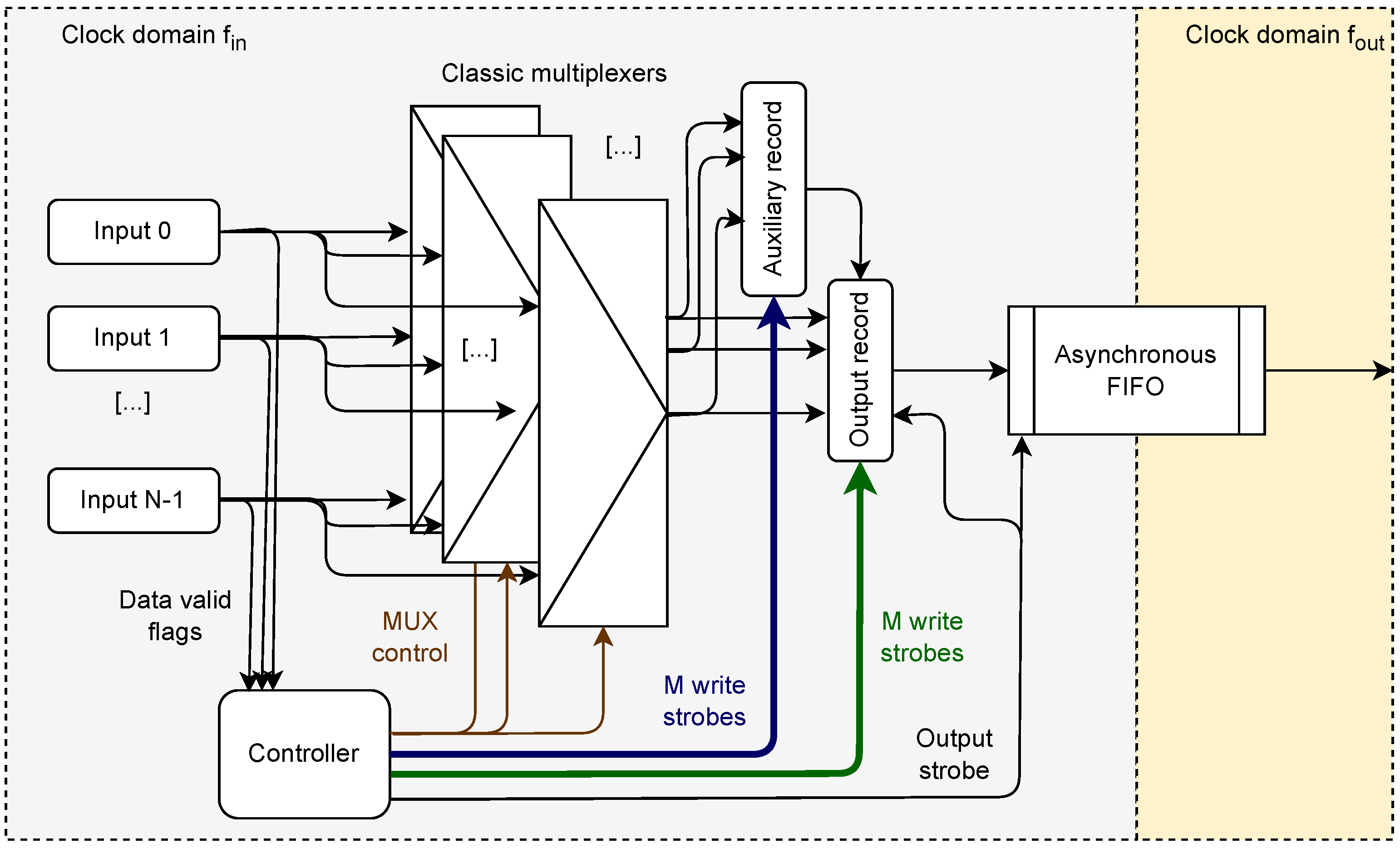
Figure 5.
The Beneš network able to perform any permutation of 8 inputs to 8 outputs [11].
Figure 5.
The Beneš network able to perform any permutation of 8 inputs to 8 outputs [11].
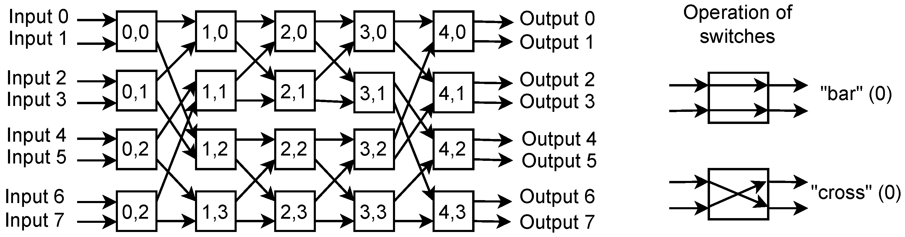
Figure 6.
General structure of the concentrator based on the Beneš network.
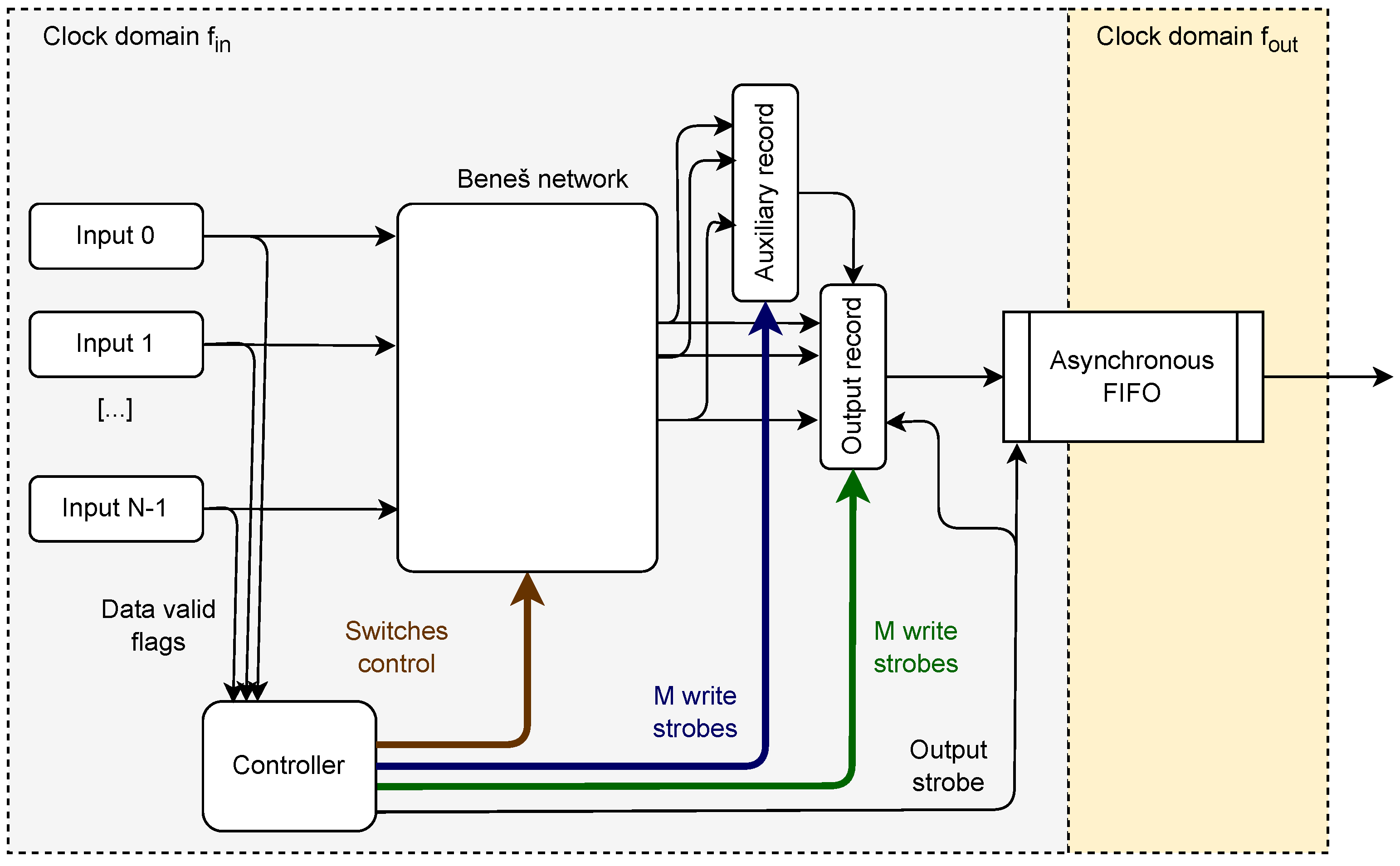
Figure 7.
Data concentrator based on 8x8 Beneš network.
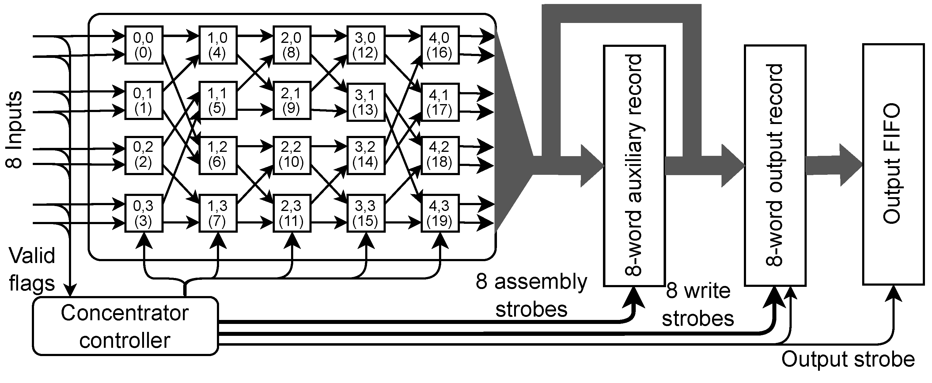
Figure 8.
Data concentrator based on a reduced 8x8 Beneš network. Not all data permutations are needed to solve the concentration problem. Only three layers appeared to be sufficient for that purpose.
Figure 8.
Data concentrator based on a reduced 8x8 Beneš network. Not all data permutations are needed to solve the concentration problem. Only three layers appeared to be sufficient for that purpose.
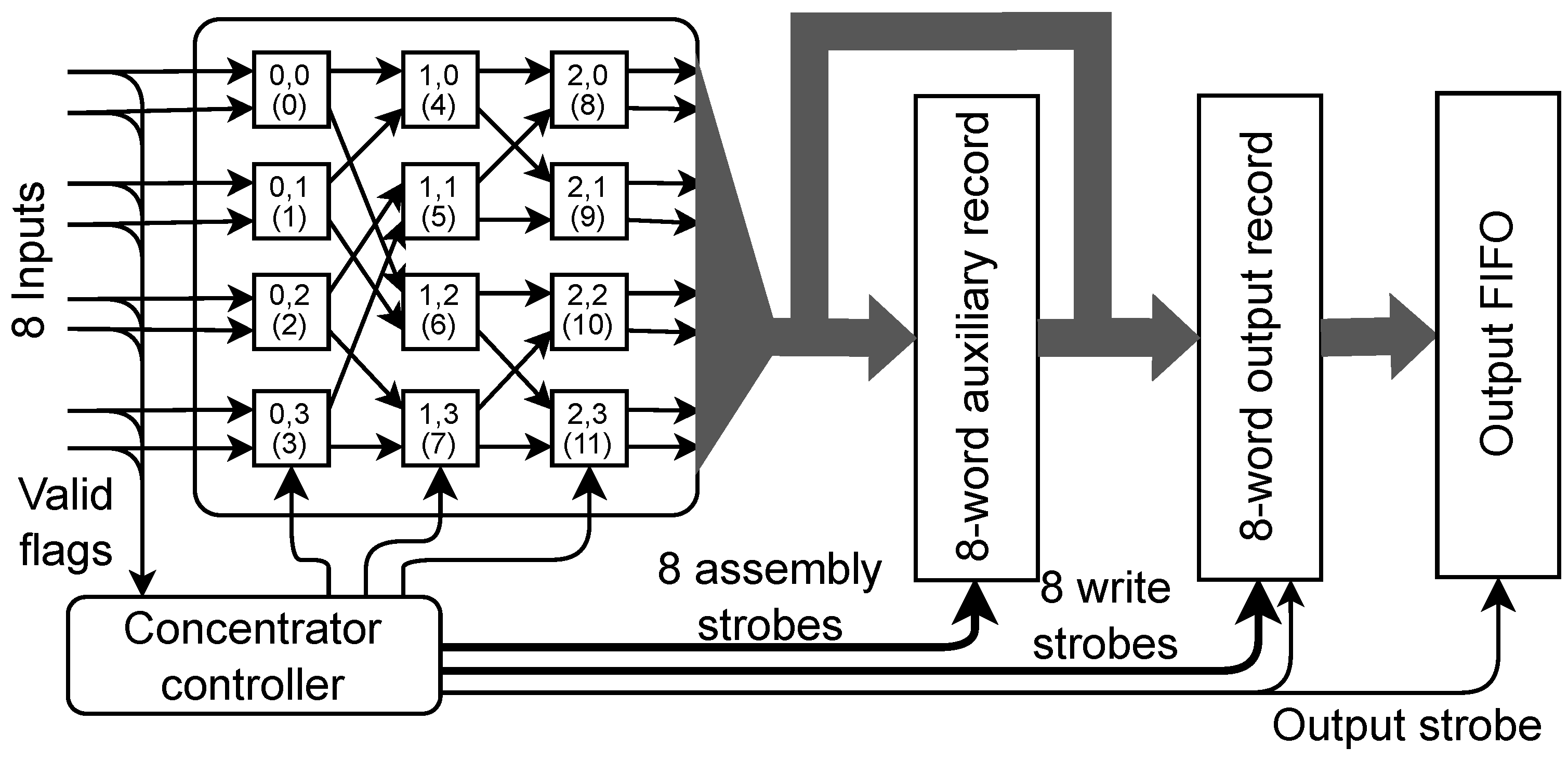
Figure 9.
Data concentrator for 7 inputs based on a Beneš network reduced to 7x8 size.

Figure 10.
Data concentrator for 12 inputs. The data width converter receives input sets containing 12 words at 160 MHz, concatenates two such sets, and outputs them as three 8-word sets at 240 MHz. Further concentration is performed as in Figure 8.
Figure 10.
Data concentrator for 12 inputs. The data width converter receives input sets containing 12 words at 160 MHz, concatenates two such sets, and outputs them as three 8-word sets at 240 MHz. Further concentration is performed as in Figure 8.
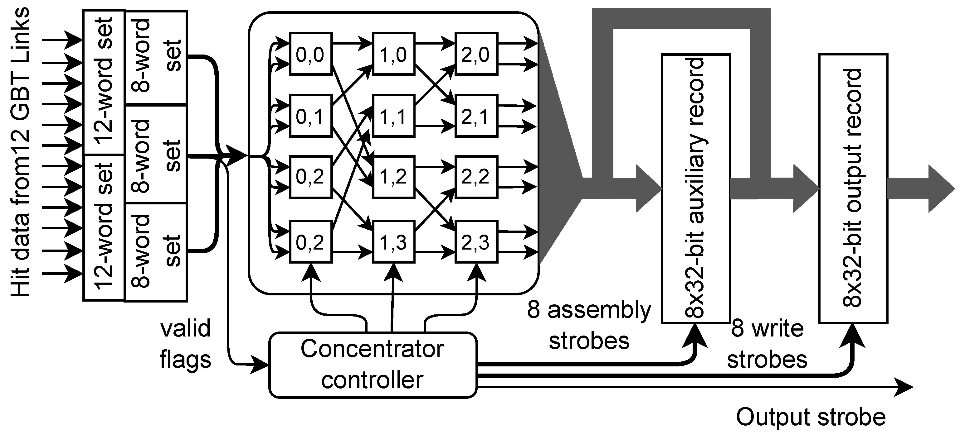
Figure 11.
Data concentrator for 9 inputs. The data width converter receives input sets containing 9 words at 160 MHz, concatenates two such sets, and outputs them as three 6-word sets at 240 MHz. Further concentration is done via a Beneš network reduced to 6x8 size. The last two inputs and the fourth switch in layer 0 are removed. Only 11 switches are controlled, like in the case of a 7x8 network.
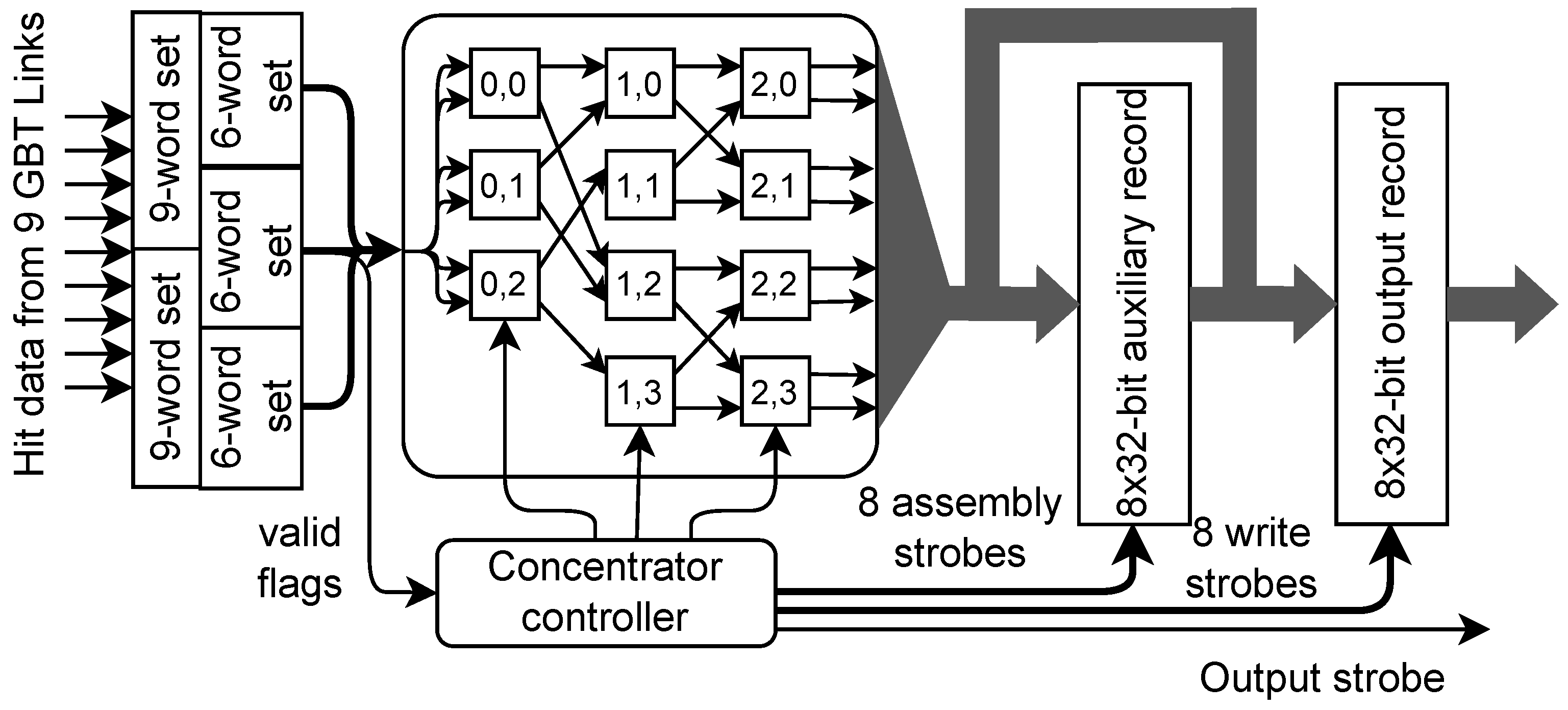
Figure 12.
Results of simulation of the concentrator with 7 inputs and probability of data presence set to 0.5.
Figure 12.
Results of simulation of the concentrator with 7 inputs and probability of data presence set to 0.5.
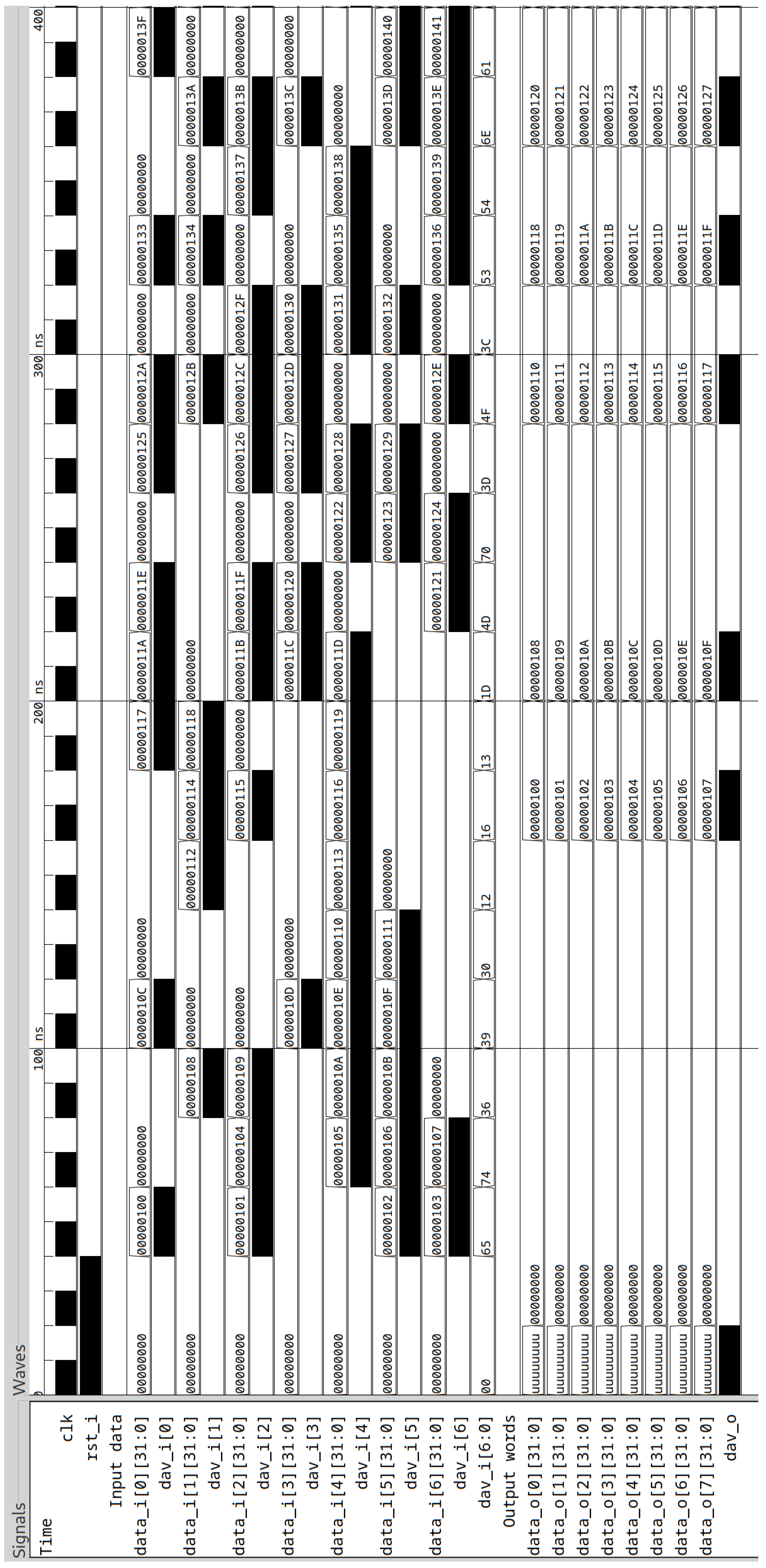
Figure 13.
Testbench for testing the concentrator in the hardware.
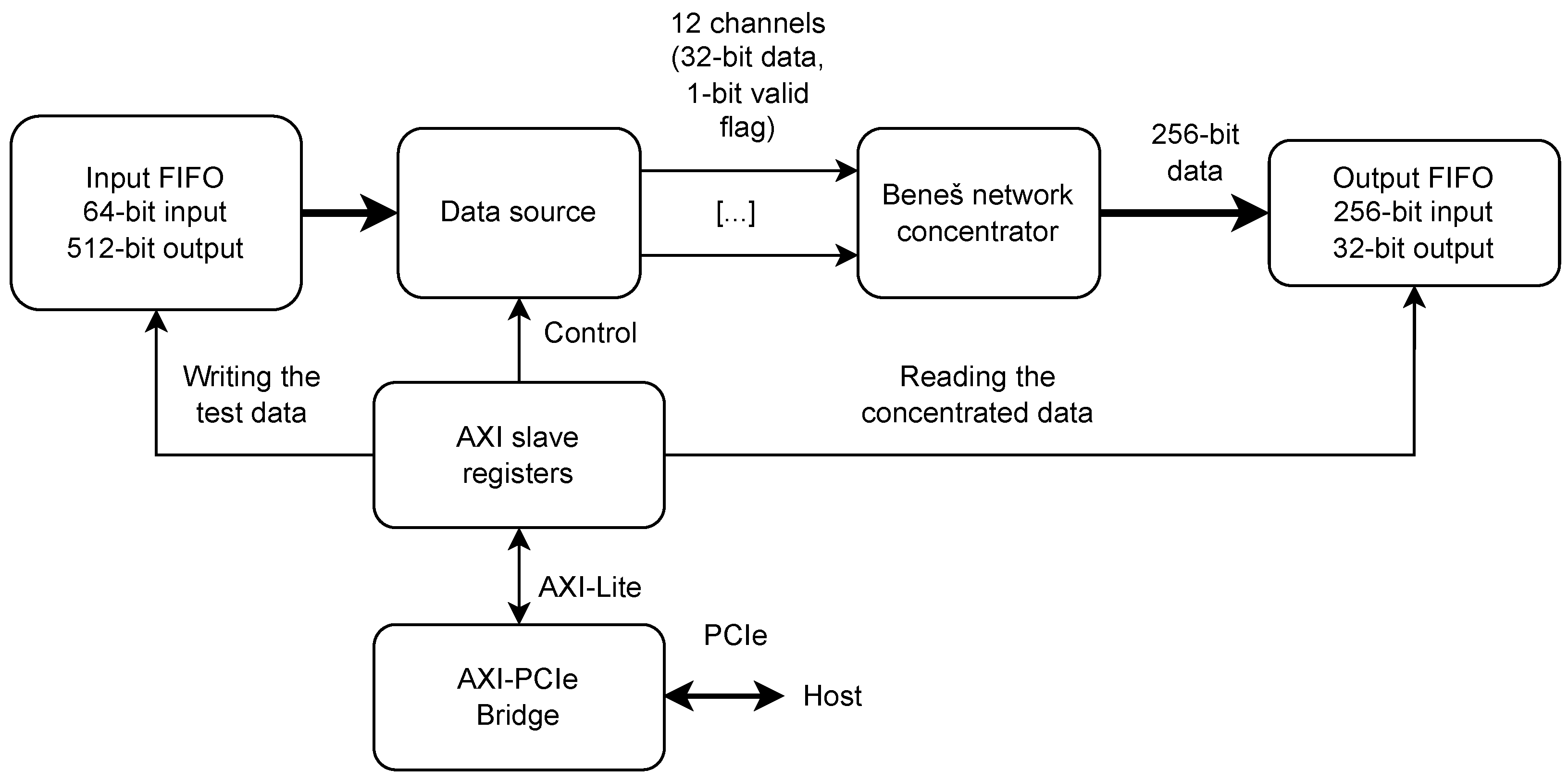

Table 1.
Width and clock frequency of AXI interface for PCI Express blocks. Results obtained from various configurations of AMD/Xilinx DMA/Bridge Subsystem for PCIe Express (4.1).
Table 1.
Width and clock frequency of AXI interface for PCI Express blocks. Results obtained from various configurations of AMD/Xilinx DMA/Bridge Subsystem for PCIe Express (4.1).
| Lane width | Maximum link speed | ||
|---|---|---|---|
| 2.5 GT/s (Gen 1) | 5 GT/s (Gen 2) | 8 GT/s (Gen 3) | |
| 1 | 64 bits @ 62.5 MHz | 64 bits @ 62.5 MHz | 64 bits @ 125 MHz |
| 64 bits @ 125 MHz | 64 bits @ 125 MHz | 64 bits @ 250 MHz | |
| 64 bits @ 250 MHz | 64 bits @ 250 MHz | ||
| 2 | 64 bits @ 62.5 MHz | 64 bits @ 125 MHz | 64 bits @ 250 MHz |
| 64 bits @ 125 MHz | 64 bits @ 250 MHz | 128 bits @ 125 MHz | |
| 64 bits @ 250 MHz | |||
| 4 | 64 bits @ 125 MHz | 128 bits @ 125 MHz | 128 bits @ 250 MHz |
| 64 bits @ 250 MHz | 64 bits @ 250 MHz | 256 bits @ 125 MHz | |
| 8 | 128 bits @ 125 MHz | 256 bits @ 125 MHz | 256 bits @ 250 MHz |
| 64 bits @ 250 MHz | 128 bits @ 250 MHz | ||
| 16 | 128 bits @ 250 MHz | 256 bits @ 250 MHz | 512 bits @ 250 MHz |
Table 2.
Resource consumption of the 12-inputs data concentrator together with the testbench for chosen hardware platforms. Absolute and percentage (in parenthesis) consumption is given. The design was synthesized in the version where no BRAM was used for the controller. Separate values for the testbench, data width converter, and concentrator itself are given. That version uses the biggest concentrator based on the 8x8 Beneš network. For all other described configurations, the resource utilization will be lower.
| KCU105 | TEC0330 | |||||
|---|---|---|---|---|---|---|
| LUTs | Flip Flops | Block RAMs | LUTs | Flip Flops | Block RAMs | |
| Available | 242400 | 484800 | 600 | 204000 | 408000 | 750 |
| Whole testbench | 7685 (3.17%) | 10641 (2.19%) | 36 (6.00%) | 10406 (5.1%) | 12339 (3.02%) | 36 (4.80%) |
| Data width converter | 745 (0.31%) | 1459 (0.30%) | 0 (0.0%) | 742 (0.36%) | 1459 (0.36%) | 0 (0.0%) |
| Data concentrator | 1038 (0.43%) | 1566 (0.32%) | 0 (0.0%) | 1032 (0.51%) | 1566 (0.38%) | 0 (0.0%) |
Disclaimer/Publisher’s Note: The statements, opinions and data contained in all publications are solely those of the individual author(s) and contributor(s) and not of MDPI and/or the editor(s). MDPI and/or the editor(s) disclaim responsibility for any injury to people or property resulting from any ideas, methods, instructions or products referred to in the content. |
© 2023 by the authors. Licensee MDPI, Basel, Switzerland. This article is an open access article distributed under the terms and conditions of the Creative Commons Attribution (CC BY) license (http://creativecommons.org/licenses/by/4.0/).
Copyright: This open access article is published under a Creative Commons CC BY 4.0 license, which permit the free download, distribution, and reuse, provided that the author and preprint are cited in any reuse.


