
Submitted:
09 January 2023
Posted:
10 January 2023
You are already at the latest version
Abstract
We report the electrical properties of Al0.3Ga0.7N/GaN heterojunction field effect transistor (HFET) structures with a Ga2O3 passivation layer grown by metal-organic chemical vapor deposition (MOCVD). In this study, three different thicknesses of Ga2O3 dielectric layers were grown on Al0.3Ga0.7N/GaN structures leading to metal-oxide-semiconductor-HFET or MOSHFET structures. X-ray diffraction (XRD) showed the (¯201) orientation peaks of -Ga2O3 in the device structure. The van der Pauw and Hall measurements yield the electron density of ~ 4 x1018 cm-3 and mobility of ~770 cm2V-1s-1 in the 2-dimensional electron gas (2DEG) channel at room temperature. Capacitance-voltage (C-V) measurement for the on-state 2DEG density for the MOSHFET structure was found to be of the order of ~1.5 x1013 cm-2. The thickness of the Ga2O3 layer was inversely related to the threshold voltage and the on-state capacitance. The interface charge density between the oxide and Al0.3Ga0.7N barrier layer was found to be of the order of ~1012 cm2eV-1. The annealing at 900° C of the MOSHFET structures revealed that the Ga2O3 layer was thermally stable at high temperatures resulting in insignificant threshold voltage shifts for annealed samples with respect to as-deposited (unannealed) structures. Our results show that the MOCVD-gown Ga2O3 dielectric layers can be a strong candidate for stable high-power devices.
Keywords:
GaN
; MOSHFET
; Ga2O3
; MOCVD
; Gate Dielectric
Introduction:
GaN-based heterojunction field effect transistors (HFETs) have excellent properties such as high critical breakdown field, high current, and superior thermal/chemical stability, which are coveted for high power, both RF and high-frequency switching applications under harsh environments [1,2,3,4]. The high-frequency performance of HFETs is limited by a series of effects associated with charge leakage, trapping/de-trapping, and conduction characteristics at different locations of the devices [5]. One of the most significant performance-limiting phenomena is the injection of electrons from the gate electrode to the surface region of the semiconductor on the drain side of the gate electrode, which results in reliability issues as well as limitations on the input drive in power applications [6,7]. For high drain and gate bias, the magnitude of the electric field under the gate region can cause tunneling/leakage of electrons from the gate metal to the semiconductor. Thus, the tunneling/gate leakage effect becomes critical for radio frequency (RF) applications because the electric field oscillates with the total terminal (dc+RF) voltage [8]. During the high voltage portion of the RF cycle, a pulse of electrons will tunnel from the gate by acquiring sufficient energy and can cause gate breakdown [9,10]. The electron transport on the surface is sluggish due to high effective mass, and dispersion is introduced due to the charging/discharging time constant [11]. The electrons escaping from the gate metal gather on the surface, creating a “virtual gate” effect that functions as an effective increase in gate length on the drain side can result in leakage current [7]. As a result, the conducting channel depletes of free electrons and device dc current and RF power decreases [7]. To overcome this problem, a dielectric material, often an oxide layer, is introduced between the metal gate and the semiconductor, creating metal-oxide-semiconductor-HFET (MOSHET) for high-frequency applications. Thus, the gate tunneling is reduced or eliminated with improved surface charge modulation by an insulating oxide layer under the gate [7,12].
The incorporation of the oxide layer improves the GaN-based HFET performance by minimizing the gate leakage current, maximizing the output power (as the input can be driven harder), improving the breakdown voltage, etc [13]. The interface between the semiconductor and oxide layer, however, plays an important role in transistor performance [14]. Chemically and thermally stable oxides with low density of interface states between the insulator (oxide) and semiconductor are required [15]. Several groups have reported the use of different dielectrics, such as aluminum oxide (Al2O3) [16], hafnium dioxide (HfO2) [17], zirconium dioxide (ZrO2) [18], silicon dioxide (SiO2) [19], silicon nitride (Si3N4), etc., fabricated by several deposition methods, including atomic layer deposition (ALD) [14], pulsed laser deposition (PLD) [20], and plasma enhanced chemical vapor deposition (PECVD) [20].
Ga2O3 is a promising material with potential dielectric applications for high-power devices because of its wide bandgap (4.4 – 5.3 eV) and high breakdown voltage (8 MVcm-1) [21,22]. It has a moderate dielectric constant (k = 10.6), which is higher than those of traditional dielectrics such as SiO2 (k = 3.9), and Si3N4 (k = 7.4) [16]. This dielectric-constant value allows gate scaling and a smaller voltage for the same charge. The feasibility of using Ga2O3 as a gate dielectric was demonstrated by employing ALD with compounds like trimethylgallium, and triethylgallium as a Ga precursor and ozone or oxygen (O2) plasma as an oxygen precursor[21,23,24]. The Ga2O3 layers grown by ALD for MOSHFETs are amorphous and prone to change their properties, especially threshold voltage, with annealing due to crystallization[25]. The use of crystalline metal-organic chemical vapor deposition (MOCVD) grown β-Ga2O3 as a gate dielectric has so far not been reported. A comprehensive study of the electrical properties is necessary to determine the feasibility of MOCVD Ga2O3 as a gate dielectric.
In this work, we study the electrical properties of Al0.3Ga0.7N/GaN HFET with MOCVD-grown β-Ga2O3 as a passivation/dielectric layer. β-Ga2O3 layers of three different thicknesses of 10 nm, 20 nm, and 30 nm were grown on top of Al0.3Ga0.7N/GaN creating MOSHFET structures. Furthermore, the variations in electrical properties, particularly the shift in threshold voltage, are studied for annealed and as-deposited MOSHFET structures with MOCVD-grown β-Ga2O3.
Experimental Methods:
The epilayers used for devices studied in this paper were deposited in a vertical cold wall metal-organic chemical vapor deposition (MOCVD) system using nitrogen (N2) as a carrier gas on a 2-inch diameter c-axis sapphire substrate with 0.2° offcut. Trimethylaluminum (TMAl), Triethylgallium (TEG), Ammonia (NH3), and ultra-high purity oxygen were used as aluminum (Al), gallium (Ga), N2, and oxygen (O2) precursors, respectively. First, a thin 150 nm aluminum nitride (AlN) buffer layer was grown on the sapphire substrate using the process described in [26,27]. Then, on top of the AlN layer, a 500 nm thick gallium nitride (GaN) channel layer with a V/III ratio of 8000 at a temperature of 960 °C, a 2 nm AlN spacer, and a 25 nm thick barrier aluminum gallium nitride (Al0.3Ga0.7N) layer with V/III ratio of 5000 at a temperature of 1020 °C were grown at 100 Torr chamber pressure, creating heterojunction field effect transistor (HFET) structure [28,29,30]. The van der Pauw and Hall effect measurements show that the GaN layers used for our device structures were highly resistive. Figure 1(a) exhibits the schematic of the HFET structure. For this study, the β-Ga2O3 layers were grown on top of the HFET structure using the MOCVD process at 700° C, 50 Torr chamber pressure, and a VI/III ratio of ~900. The details of the Ga2O3 growth can be found elsewhere [31]. This creates a MOSHFET structure with the dielectric layer thickness varying from 10 nm to 30 nm, as shown in Figure 1(b). The MOSHFET structure with 30 nm oxide thickness was annealed to gauge its electrical and thermal stability. Annealing was performed at 900° C for 30 minutes in a 50/50 O2/N2 (nitrogen was used as carrier gas) environment to avoid desorption from the Ga2O3 layer.
We characterized the structural quality and electrical properties of all the device structures obtained in this work. A Rigaku Miniflex II Desktop X-ray diffractometer with Cu-Kα1 x-ray source (λ = 1.5406 Å) operated at 30 mA current and 15 kV voltage was used to evaluate the structural properties of the epilayers. The capacitance-voltage (C-V) measurements were performed using a mercury probe controller model 802B connected with a HP 4284A Precision LCR Meter capable of measuring the impedance as a function of frequency. The gate diameter of the mercury probe was 797 μm with 0.1 pF stray capacitance. The van der Pauw/Hall effect measurements were performed on the samples using the MMR Technologies Inc. H-50 controller and MPS-50 programmable power supply with indium contacts.
Results and Discussions:
Figure 2 shows the x-ray diffraction (XRD) 2θ scan of the MOSHFET structure. The peaks at 18.8o and 38.2o are related to the (01) and (02) Ga2O3 of the β phase [32]. The peak at 34.5° and the adjacent higher angle shoulder are consistent with the (002) and (002) reflection from the GaN channel and AlGaN barrier layers, respectively [33]. Note that the GaN channel layer was grown on 0.15 µm AlN. The peak at 36.1° is due to the (002) AlN reflection. The peaks at 20.4o and 41.6o correspond to the (003) and (006) sapphire reflections [32]. The most common method of oxide dielectric deposition is ALD, which is mostly used for depositing amorphous materials[34]. The problem with amorphous layers is that, during the rapid thermal annealing (RTA) step required to form ohmic contacts to MOSHFETs, there occurs a phase transformation from amorphous to crystalline structure [25]. This transformation results in the formation of a microcrystalline structure with multiple grain boundaries, which creates leakage paths, rendering it unsuitable for device applications [25]. The process used for the MOCVD oxide deposition favors the growth of single-crystal β-Ga2O3 dielectric layers, as confirmed by the XRD data. Therefore, it is expected that, as Ga2O3 is already in the crystalline form, the thermal treatment will have a minimal impact on its electrical properties, as we demonstrate by the annealing experiments in the later description.
The origin of the highly conductive quantum confined two-dimensional electron gas (2DEG) at the AlGaN/GaN interface is due to the lack of inversion symmetry along the [0001] axis of GaN coupled with AlN being relatively more electronegative [2]. The difference between spontaneous and piezoelectric polarization and band offset at the interface introduces a fixed polarization-induced sheet of carrier charges, indicated by the shift of Fermi level in the conduction band. Schrödinger and Poisson’s equation-based charge distribution and band diagram can be calculated using different available tools [35]. However, a simpler approach using the Langer and Heinrich rule helps to estimate different parameters and understand the band structure at the heterojunction interfaces [36,37]. Figure 3 shows the schematical band diagram for the Ga2O3 MOSHFET. The bandgaps for GaN, Al0.3Ga0.7N, and Ga2O3 are 3.4 eV, 4.03 eV (using Vegard’s law), and 4.9 eV (β phase), respectively [38]. The position of the Fermi level in GaN near the channel-barrier interface is in the conduction band; where ns is the sheet carrier density, Cb is the Al0.3Ga0.7N barrier layer capacitance, Cox is the Ga2O3 layer capacitance. We can express the total gate capacitance (CG) using the series capacitance formula as below:
The capacitance-voltage (C-V) measurements of the MOSHFET structure were performed using a mercury probe gate contact to extract pertinent electrical parameters of the device structures, such as threshold voltage (Vth), zero gate voltage capacitance, and 2DEG electron density. The total gate capacitance is given by equation (1), i.e., the addition of the oxide dielectric layer capacitance in series with the barrier layer capacitance. The benefit of an oxide dielectric is to increase the gate breakdown voltage and/or reduce the gate leakage current by suppressing the surface states, sometimes, superseded by the impact of different device electrical parameters such as threshold voltage and gate leakage current. The threshold voltage of the MOSHFET structure is given by the equation [39] :
where and are the threshold voltage of the MOSHFET and HFET (that without the oxide layer- otherwise identical), respectively. , , and are the thicknesses and dielectric constants of the insulator/oxide (indexed by i) and semiconductor barrier (indexed by s,b) layers, respectively. From equation (2), it is clear that if increases, increases, whereas decreases with the increase of ,. Thus, a higher dielectric constant and lower dielectric thickness are desirable for minimum threshold voltage shifts.
Figure 4 (a) shows the C-V data for HFET and MOSHFET structures with oxide thicknesses of 10 nm, 20 nm, and 30 nm. The addition of oxide on the HFET barrier adds capacitance in series with the existing barrier layer capacitance, which would lower the overall gate capacitance. The relative dielectric constants for the AlGaN barrier layer (9.2) and that for the Ga2O3 (10.6) are very close [40]. We did not observe any change in the C-V curve shape near the zero-gate voltage position when increasing the negative gate voltage before depleting the channel. From equation (2), we observe that as the thickness of the oxide layer increases, the Vth should increase. The CV measurements on the MOSHFET structure with MOCVD-grown Ga2O3 gate dielectric confirm the increase in the Vth value. As the thickness of the Ga2O3 layer increased, the Vth exhibited a negative shift. Thus, with the increase of dielectric layer thickness, a higher voltage is required to deplete the 2DEG. During the C-V measurement, when 2DEG starts to deplete, the capacitance decreases drastically, ultimately leading to pinching off of the channel. By further increasing the gate voltage beyond pinch-off, the depletion layer extends to the GaN channel. Figure 4 (b) summarizes the above discussion.
Figure 5 compares the C-V data for annealed and as-deposited MOSHFETs with a 30 nm thick β-Ga2O3 as a gate oxide layer. The 30-min annealing at 900 ºC was performed in the MOCVD reactor, used for the Ga2O3 growth, as described in the experimental method section. As can be concluded from the data, the annealing experiment did not result in any discernable change in the Vth and zero capacitance values, demonstrating the excellent thermal stability of the crystalline β-Ga2O3. The change in threshold voltage (open circle) and capacitance (open square) for the annealed MOSHFET structure are also shown in Figure 4 (b).
The carrier density Nd was calculated using the Hall effect data and found to be on the order of 1018 cm-3 – the exact values of the carrier density can be found in Table 1. The built-in voltage Vbi (as shown in the band diagram: Figure 2) can be measured from 1/C2 intercept with the x-axis and expressed by equation (3) [41]:
Here, and are the thickness and permittivity of the oxide layer, is the carrier concentration, and are the depletion width and permittivity of the AlGaN barrier layer. If we set = 0, then the 2nd and 3rd term of equation (3) becomes zero, and the equation represents the built-in voltage for conventional HFET structure. Using equation (1) and the parallel plate capacitance formula for each series capacitor component, we can calculate the value of at zero gate voltage. Inserting the determined value of , and previously calculated/measured , , and known , into Equation (3), we can obtain the oxide charge . The calculated values of for all the samples is shown in Table 1. We observe a trend in the value of ; As the oxide thickness increases, the value of , become more negative which increases Vth shift supporting equation 2.
Figure 6 shows the 2DEG carrier density (ns) versus the gate voltage (VG) for 10, 20 and 30 nm gate oxide thicknesses calculated using the following equation:
qns = (VG - Vth) CG
In all three cases, the zero-gate voltage value of sheet carrier density is very close in the range of (1.25-1.5)×1013 cm-2, a slightly higher value of ns could be due to sample-to-sample variations. The sheet carrier concentrations measured using van der Pauw/Hall effect method are also in the range of (1-1.5)×1013 cm-2, which validates our calculations using the value from the C-V measurement by employing equation (4). The sheet carrier concentration does not change with oxide layer thickness or annealing of the oxide layer. In previous studies for the ALD-grown amorphous oxide dielectrics-based MOSHFETs, it has been demonstrated that the annealing of the oxide layers drastically shifts Vth. As we can see in Figure 5, annealing of the crystalline Ga2O3-based MOSHFET, there is no noticeable change in the threshold voltage in contrast to the case for ALD-grown oxides [42]. To further validate the MOCVD oxide material property we can use equation (1), to calculate the experimental dielectric constant for β-Ga2O3. The values of the gate capacitance, CG, before and after annealing are 1.64×10⁻⁷ F/cm-2 and 1.67×10⁻⁷ F/cm-2 (for 1 MHz frequency measurement). Cb is the barrier capacitance of the MOSHFET, and the value is 3.3×10⁻⁷ F/cm-2. Based on , we get 10.9 (using CG = 1.67×10⁻⁷ F/cm-2), whereas the reference value is 10.6. Thus, it can be inferred that the MOCVD-grown oxide has a dielectric property that is very close to the previously reported literature value [40].
The interface trapped charge or interface traps stem(s) from dangling bonds at the semiconductor–insulator interface. The frequency-dependent High-Low method is commonly used to determine interface charge density (Dit). Figure 7 shows the frequency-dependent CV measurement used to calculate the interface charge densities for MOSHFET with 10 nm oxide thickness (the frequency-dependent C-V measurements of MOSHFET with 20 nm, 30 nm oxide thickness and the annealed sample are shown in the Supplementary section).
The High-Low frequency CV method compares a low-frequency C-V curve with one that is free of interface traps. The latter is usually referred to as a high-frequency C-V measurement, where interface traps with relatively long-time constants cannot respond, leading to decreased measured capacitance. At low frequencies, the interface traps can respond, if not deep, thus resulting in higher capacitance; 100 kHz and 1 MHz frequencies are the typical values can be used for CV-based calculations of the density of interface states (Dit) of Nitride systems [45]. Consequently, from the difference between high- and low-frequency CV measurements, the Dit can be obtained based on equation (5) at a specific applied gate voltage [43]:
Where is the capacitance of the oxide dielectric layer calculated using the parallel plate capacitor formula, is the unit elementary charge, is the MOSHFET low-frequency capacitance value and is the MOSHFET high-frequency capacitance value. The total trap densities for all the samples are tabulated in Table I. For all samples, the calculated interface trap densities are in the range (3-7.57) × 1012 cm-2eV-1; these values are close to the typically calculated values of MOSHFETs (typical values are in the order of ~1011 cm-2eV-1 -1013 cm-2eV-1) [25]. The Dit value is expected to be lower for the processed devices due to the mesa isolation [44]. Our data revealed no specific correlation between the oxide thickness and interface trap densities. Ideally, this is the case, but the total number of bulk defects in the oxide under the gate would depend on the thickness, more data are needed to find any correlation. It is observed that the annealed sample showed a slightly smaller trap density, which can correlate to the higher ns, the origin of which is not yet explored. Table I summarizes the key electrical parameters of the GaN/AlGaN-based HFET and GaN/AlGaN/βGa2O3-based MOSHFET determined in this work.

Table 1.
The summary of the key electrical parameters measured/calculated from C-V and Hall measurements.
Table 1.
The summary of the key electrical parameters measured/calculated from C-V and Hall measurements.
| Vth (V) |
µ (cm2V-1 s-1) (Hall) |
Rsh (Ωcm-2) (Hall) |
Nd (cm-3) (Hall) |
ns (cm-2) (C-V) |
ns (cm-2) (Hall) |
Qox (Ccm-2) (C-V) |
Dit (cm-2eV-1) (C-V) |
|
|---|---|---|---|---|---|---|---|---|
| HFET | -5 | 750 | 537 | 6.8×10¹⁸ | 1.25×10¹³ | 1.55×10¹³ | None | None |
| 10 nm | -7.9 | 772 | 630 | 5.0×10¹⁸ | 1.28×10¹³ | 1.4×10¹³ | -6.68×10¹² | 7.47×10¹² |
| 20 nm | -9.5 | 770 | 650 | 4.2×10¹⁸ | 1.24×10¹³ | 1.42×10¹³ | -1.64×10¹³ | 7.57×10¹² |
| 30 nm | -12.5 | 776 | 685 | 4.4×10¹⁸ | 1.4×10¹³ | 1.4×10¹³ | -2×10¹³ | 4.98×10¹² |
| annealed | -12.1 | 760 | 680 | 4.5×10¹⁸ | 1.4×10¹³ | 1.4×10¹³ | -3.06×10¹² | 3×10¹² |
Conclusions:
We have demonstrated MOCVD-grown single-crystal Ga2O3 thin films as a gate dielectric on AlGaN/GaN HFETs. We have found that an increase in the thickness of the dielectric layer has an impact on threshold voltage Vth, shifting it to more negative values and reducing the zero capacitance as additional Cox is added in series. The sheet carrier densities for HFET and MOSHFETs were determined to be ~1013 cm-2, well within the typical range- of 1012 cm-2 - 1013 cm-2 for AlGaN/GaN-based devices. Moreover, the addition of the oxide layer did not change the sheet carrier concentration but had an impact on the calculated value of oxide charge Qox. The calculated Qox value was found to be negative and mainly responsible for depleting the 2DEG. As the thickness of the Ga2O3 layer increases, the Qox becomes more negative, following a trend similar to the change of Vth with increasing gate oxide thickness. The charge density in the oxide-AlGaN barrier interface was found to be of the order of ~1012 cm2eV-1. The thermal stability, as confirmed by the annealing experiment, suggests that the MOCVD-grown single-crystal Ga2O3 layer could be more suitable for the gate dielectric application compared to the ALD-grown oxide due to threshold voltage stability. The moderate interface trap density and good thermal stability indicate that MOCVD-grown β-Ga2O3 is an excellent candidate for gate dielectric as well as a passivation layer for III-Nitride-based high-power RF MOSHFET devices.
Supplementary Materials
The following supporting
information can be downloaded at the website of this paper posted on Preprints.org. Figure S1. Frequency-dependent CV measurements of MOSHFET with (a) 20 nm thick gate oxide (b) 30 nm thick gate oxide, and (c) annealed 30 nm thick gate oxide.
Author Contributions
S.H.: Conceptualization of this study, Experimentation, Data curation, Methodology, Writing–original draft, M. J.: Revision, Experimentation, S.C.: Revision, Experimentation, Editing, D.L.: Revision, Experimentation, Editing, V.A.: Revision, Editing, U.O.: Revision, Editing, H.M.: Revision, Editing, I.A.: Conceptualization of this study, Visualization, Editing, Revision, PI of this study.
Acknowledgments
This research was supported by National Science Foundation (NSF) award No. 2124624 managed by Dr. Dominique M. Dagenais.
Data availability
The data generated during and/or analyzed during the current study are available from the corresponding authors on reasonable request.
Conflicts of Interest
The authors declare that they have no conflict of interest.
References
- Morkoç, H. Handbook of Nitride Semiconductors and Devices, Materials Properties, Physics and Growth; 2009; Wiley-VCH GmbH, Weinhem, Germany. ISBN 9783527408375.
- Mohammad SN, Salvador AA, Morkoc H. Emerging gallium nitride-based devices. Proceedings of the IEEE. 1995; 83(10):1306-55. [CrossRef]
- Morkoç, H. Nitride Semiconductors and Devices; 1999, Springer-Verlag, Berlin Heidelberg, New York, ISBN 3-540-64038.
- Zeng, F.; An, J.X.; Zhou, G.; Li, W.; Wang, H.; Duan, T.; Jiang, L.; Yu, H. A Comprehensive Review of Recent Progress on GaN High Electron Mobility Transistors: Devices, Fabrication and Reliability. Electronics 2018, Vol. 7, Page 377 2018, 7, 377, doi:10.3390/ELECTRONICS7120377. [CrossRef]
- Islam, N.; Mohamed, M.F.P.; Khan, M.F.A.J.; Falina, S.; Kawarada, H.; Syamsul, M. Reliability, Applications and Challenges of GaN HEMT Technology for Modern Power Devices: A Review. Crystals (Basel) 2022, 12, 1581, doi:10.3390/cryst12111581. [CrossRef]
- Kim, H.; Lee, J.; Liu, D.; Lu, W. Gate Current Leakage and Breakdown Mechanism in Unpassivated AlGaNGaN High Electron Mobility Transistors by Post-Gate Annealing. Appl Phys Lett 2005, 86, 1–3, doi:10.1063/1.1899255. [CrossRef]
- Leach, J.H.; Morkoç, H. Status of Reliability of GaN-Based Heterojunction Field Effect Transistors. In Proceedings of the IEEE; Institute of Electrical and Electronics Engineers Inc., 2010; Vol. 98, pp. 1127–1139. [CrossRef]
- Purnachandra Rao, G.; Singh, R.; Lenka, T.R. Performance Analysis of AlGaN/GaN HEMT for RF and Microwave Nanoelectronics Applications. 2023, 139–153, doi:10.1007/978-981-19-2165-0_11. [CrossRef]
- Trew RJ. Wide bandgap semiconductor transistors for microwave power amplifiers. IEEE Microwave magazine. 2000 ;1(1):46-54. [CrossRef]
- Brar B, Boutros K, DeWarnes RE, Tilak V, Shealy R, Eastman L. Impact ionization in high performance AlGaN/GaN HEMTs. In Proceedings. IEEE Lester Eastman Conference on High Performance Devices 2002 (pp. 487-491).
- Trew RJ, Green DS, Shealy JB. AlGaN/GaN HFET reliability. IEEE Microwave magazine. 2009;10(4):116-27. [CrossRef]
- Zhou, H.; Lou, X.; Sutherlin, K.; Summers, J.; Kim, S.B.; Chabak, K.D.; Gordon, R.G.; Ye, P.D. DC and RF Performance of AlGaN/GaN/SiC MOSHEMTs with Deep Sub-Micron T-Gates and Atomic Layer Epitaxy MgCaO as Gate Dielectric. IEEE Electron Device Letters 2017, 38, 1409–1412. [CrossRef]
- Liu C, Chor EF, Tan LS. Investigations of Hf O 2∕ Al Ga N∕ Ga N metal-oxide-semiconductor high electron mobility transistors. Applied physics letters. 2006; 88(17):173504. [CrossRef]
- Asubar JT, Yatabe Z, Gregusova D, Hashizume T. Controlling surface/interface states in GaN-based transistors: Surface model, insulated gate, and surface passivation. Journal of Applied Physics. 2021; 129(12):121102. [CrossRef]
- Lee BH, Kang L, Nieh R, Qi WJ, Lee JC. Thermal stability and electrical characteristics of ultrathin hafnium oxide gate dielectric reoxidized with rapid thermal annealing. Applied Physics Letters. 2000; 76(14):1926-8. [CrossRef]
- Gusev EP, Copel M, Cartier E, Baumvol IJ, Krug C, Gribelyuk MA. High-resolution depth profiling in ultrathin Al 2 O 3 films on Si. Applied Physics Letters. 2000; 76(2):176-8. [CrossRef]
- Lee BH, Kang L, Nieh R, Qi WJ, Lee JC. Thermal stability and electrical characteristics of ultrathin hafnium oxide gate dielectric reoxidized with rapid thermal annealing. Applied Physics Letters. 2000; 76(14):1926-8. [CrossRef]
- Copel M, Gribelyuk M, Gusev E. Structure and stability of ultrathin zirconium oxide layers on Si (001). Applied Physics Letters. 2000; 76(4):436-8. [CrossRef]
- Husna, F.; Lachab, M.; Sultana, M.; Adivarahan, V.; Fareed, Q.; Khan, A. High-Temperature Performance of AlGaN/GaN MOSHEMT with SiO2 Gate Insulator Fabricated on Si (111) Substrate. IEEE Trans Electron Devices 2012, 59, 2424–2429, doi:10.1109/TED.2012.2204888. [CrossRef]
- Balakrishnan G, Babu RV, Shin KS, Song JI. Growth of highly oriented γ-and α-Al2O3 thin films by pulsed laser deposition. Optics & Laser Technology. 2014; 56:317-21. [CrossRef]
- Passlack M, Schubert EF, Hobson WS, Hong M, Moriya N, Chu SN, Konstadinidis K, Mannaerts JP, Schnoes ML, Zydzik GJ. Ga2O3 films for electronic and optoelectronic applications. Journal of applied physics. 1995; 77(2):686-93. [CrossRef]
- Green, A.J.; Speck, J.; Xing, G.; Moens, P.; Allerstam, F.; Gumaelius, K.; Neyer, T.; Arias-Purdue, A.; Mehrotra, V.; Kuramata, A.; et al. β-Gallium Oxide Power Electronics. APL Mater 2022, 10, doi:10.1063/5.0060327. [CrossRef]
- Choi DW, Chung KB, Park JS. Low temperature Ga2O3 atomic layer deposition using gallium tri-isopropoxide and water. Thin Solid Films. 2013; 546:31-4. [CrossRef]
- Donmez I, Ozgit-Akgun C, Biyikli N. Low temperature deposition of Ga2O3 thin films using trimethylgallium and oxygen plasma. Journal of Vacuum Science & Technology A: Vacuum, Surfaces, and Films. 2013; 31(1):01A110. [CrossRef]
- Hashizume, T.; Nishiguchi, K.; Kaneki, S.; Kuzmik, J.; Yatabe, Z. State of the Art on Gate Insulation and Surface Passivation for GaN-Based Power HEMTs. Mater Sci Semicond Process 2018, 78, 85–95. [CrossRef]
- Hasan, S.; Mamun, A.; Hussain, K.; Gaevski, M.; Ahmad, I.; Khan, A. Growth Evolution of High-Quality MOCVD Aluminum Nitride Using Nitrogen as Carrier Gas on the Sapphire Substrate. J Mater Res 2021, 36, 4360–4369, doi:10.1557/s43578-021-00387-z. [CrossRef]
- Hasan, S.; Mamun, A.; Hussain, K.; Patel, D.; Gaevski, M.; Ahmad, I.; Khan, A. Investigation of MOCVD Grown Crack-Free 4 Μm Thick Aluminum Nitride Using Nitrogen as a Carrier Gas. MRS Adv 2021, 6, 456–460, doi:10.1557/s43580-021-00071-8. [CrossRef]
- Shrestha, N.; Shrestha, N.M.; Wang, Y.Y.; Li, Y.; Chang, E.Y. Effect of AlN Spacer Layer on AlGaN/GaN HEMTs; 2013; ISBN 978-3-901578-26-7.
- Hubáček, T.; Hospodková, A.; Kuldová, K.; Slavická Zíková, M.; Pangrác, J.; Čížek, J.; Liedke, M.O.; Butterilng, M.; Wagner, A.; Hubík, P.; et al. Improvement of Luminescence Properties of N-GaN Using TEGa Precursor. J Cryst Growth 2020, 531, 125383, doi:10.1016/j.jcrysgro.2019.125383. [CrossRef]
- Roy, P.; Jawanpuria, S.; Vismita; Prasad, S.; Islam, A. Characterization of AlGaN and GaN Based HEMT with AlN Interfacial Spacer. In Proceedings of the Proceedings - 2015 5th International Conference on Communication Systems and Network Technologies, CSNT 2015; Institute of Electrical and Electronics Engineers Inc., 2015; pp. 786–788.
- Jewel, MU, Hasan, S., Crittenden, S., Avrutin V, Özgür Ü, Morkoç H., Ahmad, I., Growth of Thick Phase-Pure β-Ga2O3 on a c-Plane Sapphire Substrate Using MOCVD. Submitted Manuscript 2022.
- Ghose, S.; Rahman, S.; Hong, L.; Rojas-Ramirez, J.S.; Jin, H.; Park, K.; Klie, R.; Droopad, R. Growth and Characterization of β-Ga2O3 Thin Films by Molecular Beam Epitaxy for Deep-UV Photodetectors. J Appl Phys 2017, 122, doi:10.1063/1.4985855. [CrossRef]
- Moram MA, Vickers ME. X-ray diffraction of III-nitrides. Reports on progress in physics. 2009 Feb 20;72(3):036502. [CrossRef]
- George, S.M. Atomic Layer Deposition: An Overview. Chem Rev 2010, 110, 111–131, doi:10.1021/CR900056B. [CrossRef]
- M Grundmann, BandEng. 2005. http://my.ece.ucsb.edu/mgrundmann/.
- Langer JM, Heinrich H. Deep-level impurities: A possible guide to prediction of band-edge discontinuities in semiconductor heterojunctions. Physical review letters. 1985; 55(13):1414. [CrossRef]
- Jena, D. Polarization Induced Electron Populations in III-V Nitride Semiconductors Transport, Growth, and Device Applications; 2003, Doctoral Dissertation, University of California Santa Barbara.
- Langer JM, Delerue C, Lannoo M, Heinrich H. Transition-metal impurities in semiconductors and heterojunction band lineups. Physical Review B. 1988; 38(11):7723. [CrossRef]
- Rai S, Adivarahan V, Tipirneni N, Koudymov A, Yang J, Simin G, Khan MA. Low threshold-14 W/mm ZrO2/AlGaN/GaN metal–oxide–semiconductor heterostructure field effect transistors. Japanese journal of applied physics. 2006;45(6R):4985. [CrossRef]
- Shih, H.Y.; Chu, F.C.; Das, A.; Lee, C.Y.; Chen, M.J.; Lin, R.M. Atomic Layer Deposition of Gallium Oxide Films as Gate Dielectrics in AlGaN/GaN Metal–Oxide–Semiconductor High-Electron-Mobility Transistors. Nanoscale Res Lett 2016, 11, doi:10.1186/S11671-016-1448-Z. [CrossRef]
- Sze, S.; Li, Y.; Ng, K. Physics of Semiconductor Devices; John Wiley & Sons, Inc., 2021.
- Mollah S, Hussain K, Mamun A, Alam MD, Chandrashekhar MV, Simin G, Khan A. Threshold voltage control with high-temperature gate-oxide annealing in ultrawide bandgap AlGaN-channel MOSHFETs. Applied Physics Express. 2022;15(10):104001. [CrossRef]
- Schroder, D.K. Frontmatter. In Semiconductor Material and Device Characterization; John Wiley & Sons, Inc., 2005.
- Remesh, N.; Kumar, S.; Guiney, I.; Humphreys, C.J.; Raghavan, S.; Muralidharan, R.; Nath, D.N. A Novel Technique to Investigate the Role of Traps in the Off-State Performance of AlGaN/GaN High Electron Mobility Transistor on Si Using Substrate Bias. Physica Status Solidi (A) Applications and Materials Science 2020, 217, doi:10.1002/PSSA.201900794. [CrossRef]
- Osvald J. Interface traps contribution to capacitance of Al2O3/(GaN) AlGaN/GaN heterostructures at low frequencies. Physica E: Low-dimensional Systems and Nanostructures. 2017; 93:238-42. [CrossRef]
Figure 1.
The epilayer structure of the (a) Al0.3Ga0.7N/GaN HFET, (b) Ga2O3 MOSHFET.
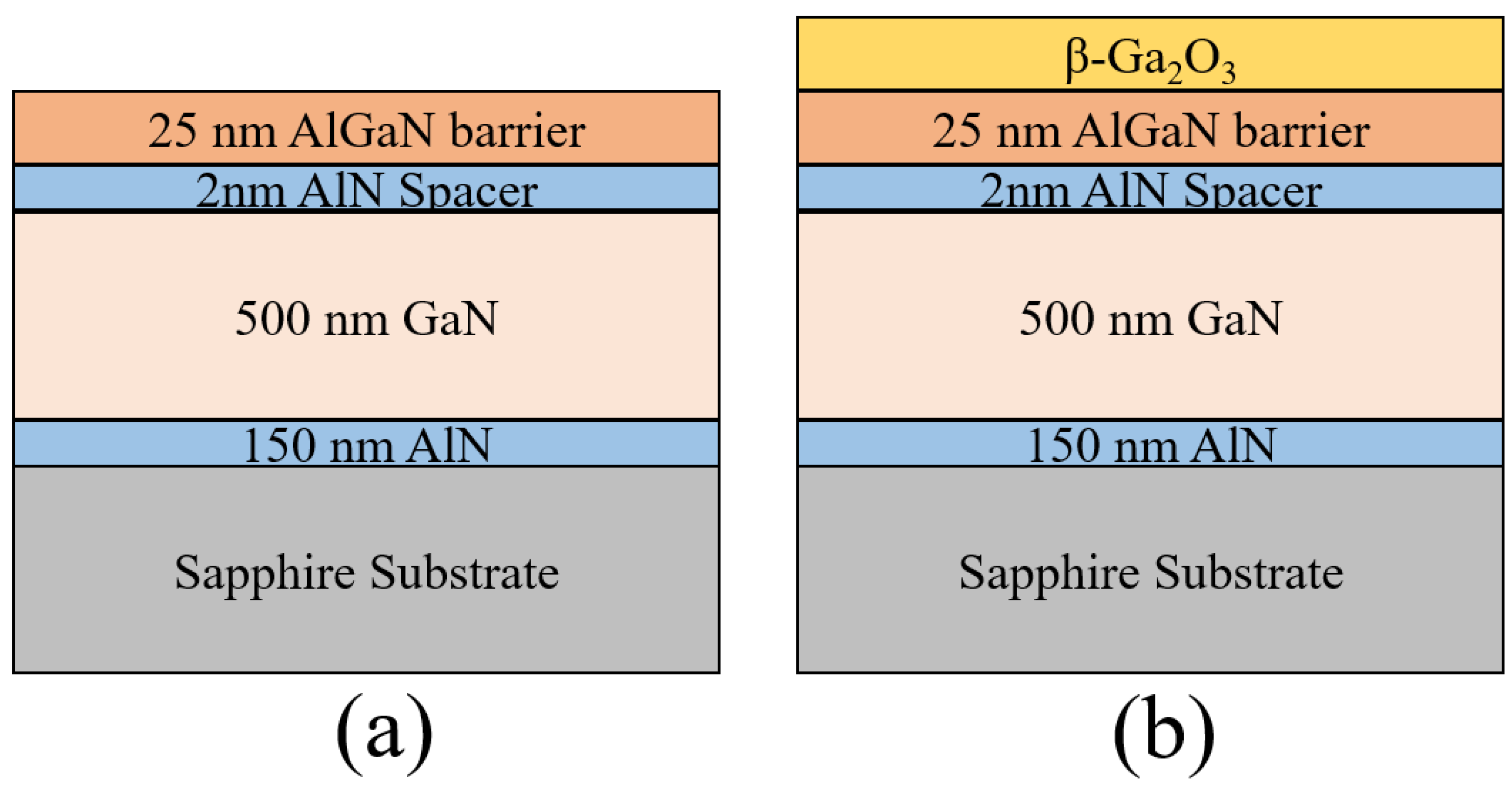
Figure 2.
XRD 2θ scan of the MOSHFET structure confirming the presence of the peaks consistent with crystalline Ga2O3 (β phase), GaN, AlGaN, AlN, and sapphire substrate. .
Figure 2.
XRD 2θ scan of the MOSHFET structure confirming the presence of the peaks consistent with crystalline Ga2O3 (β phase), GaN, AlGaN, AlN, and sapphire substrate. .
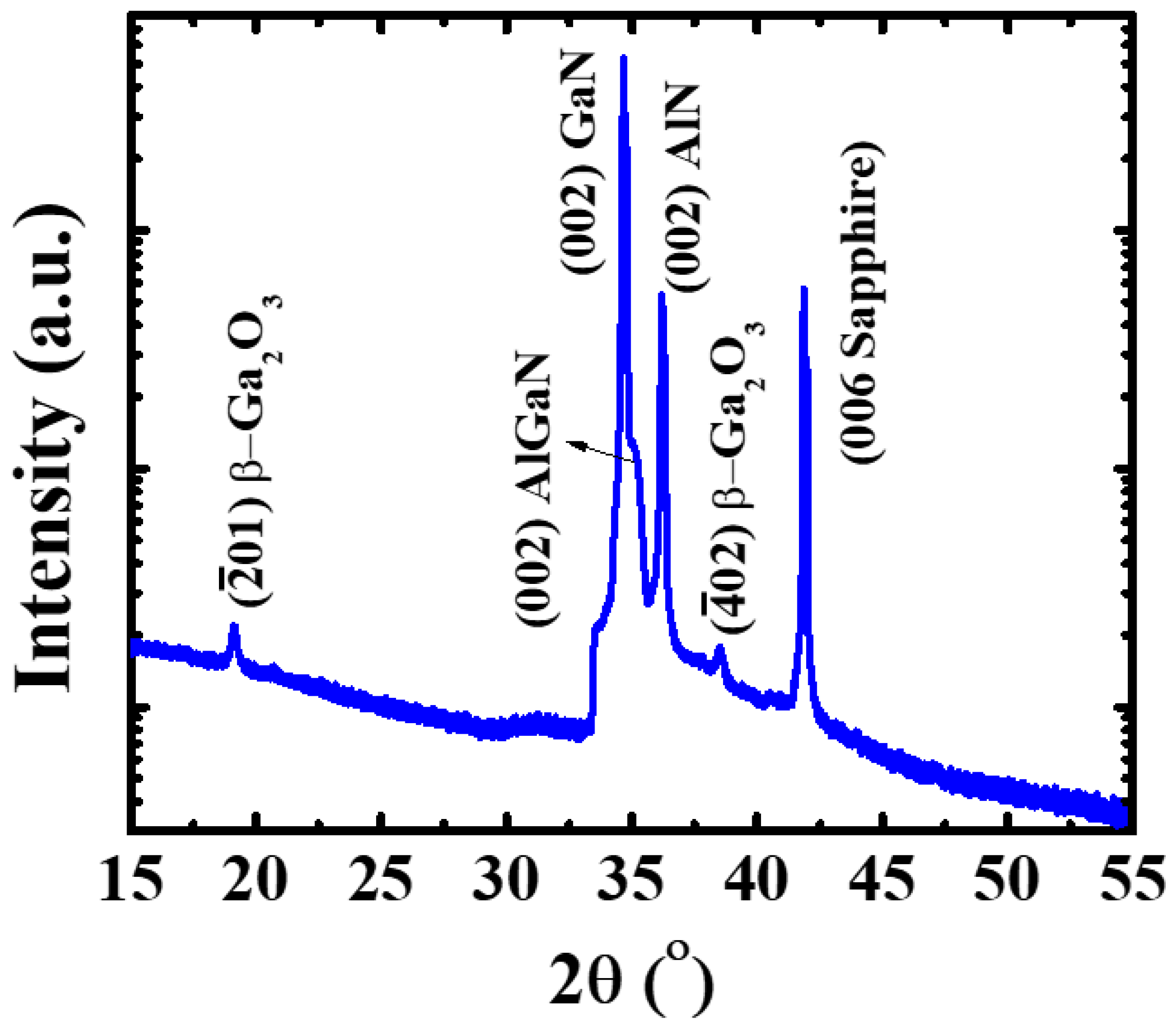
Figure 2.
The representative band diagram of GaN/AlGaN MOSHFET with Ga2O3 as a gate dielectric.
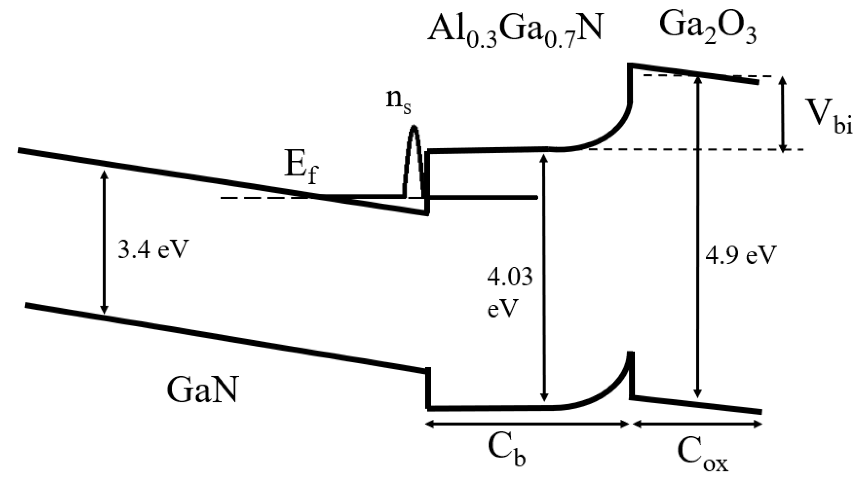
Figure 4.
C-V characteristics at 1MHz frequency of (a) HFET and Ga2O3-based MOSHFETs with different oxide thicknesses, (b) Threshold voltage and zero gate-voltage capacitance dispersion for HFET and Ga2O3 MOSHFETs.
Figure 4.
C-V characteristics at 1MHz frequency of (a) HFET and Ga2O3-based MOSHFETs with different oxide thicknesses, (b) Threshold voltage and zero gate-voltage capacitance dispersion for HFET and Ga2O3 MOSHFETs.
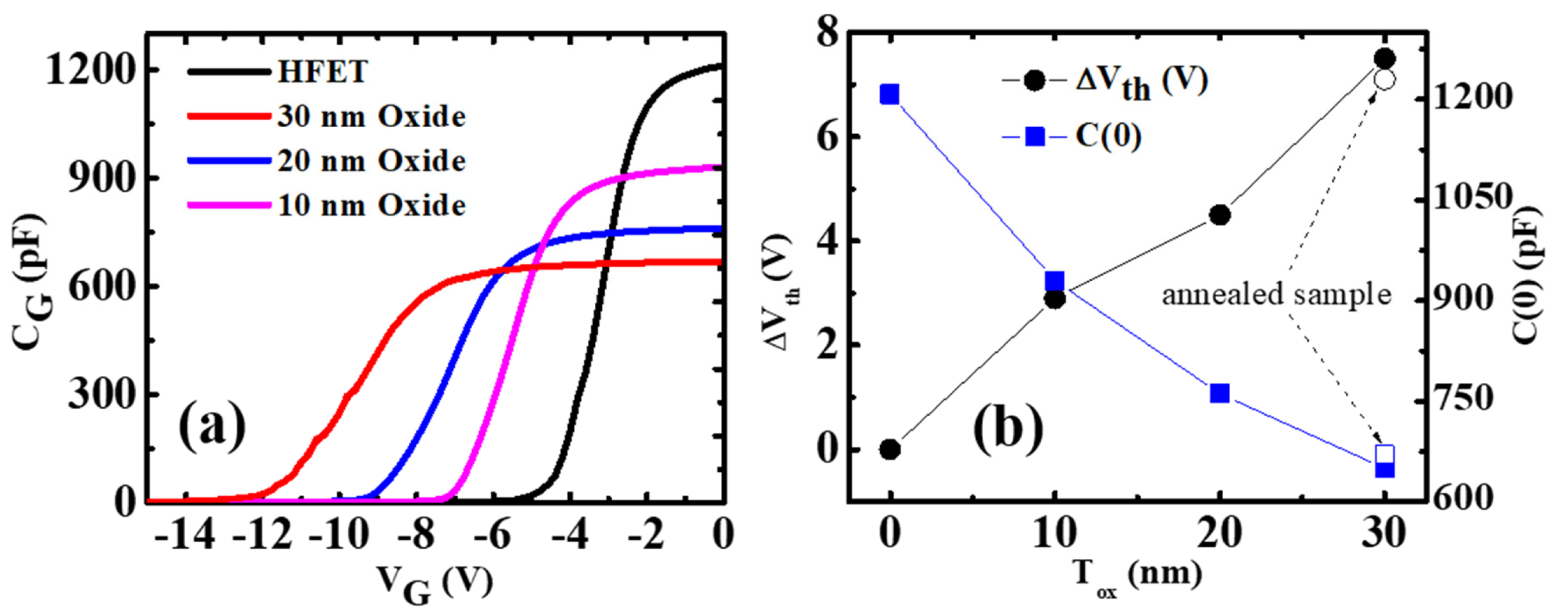
Figure 5.
C-V data of at 1MHz frequency Ga2O3-based MOSHFET with 30 nm oxide thickness annealed (dashed line) and unannealed (continuous line).
Figure 5.
C-V data of at 1MHz frequency Ga2O3-based MOSHFET with 30 nm oxide thickness annealed (dashed line) and unannealed (continuous line).
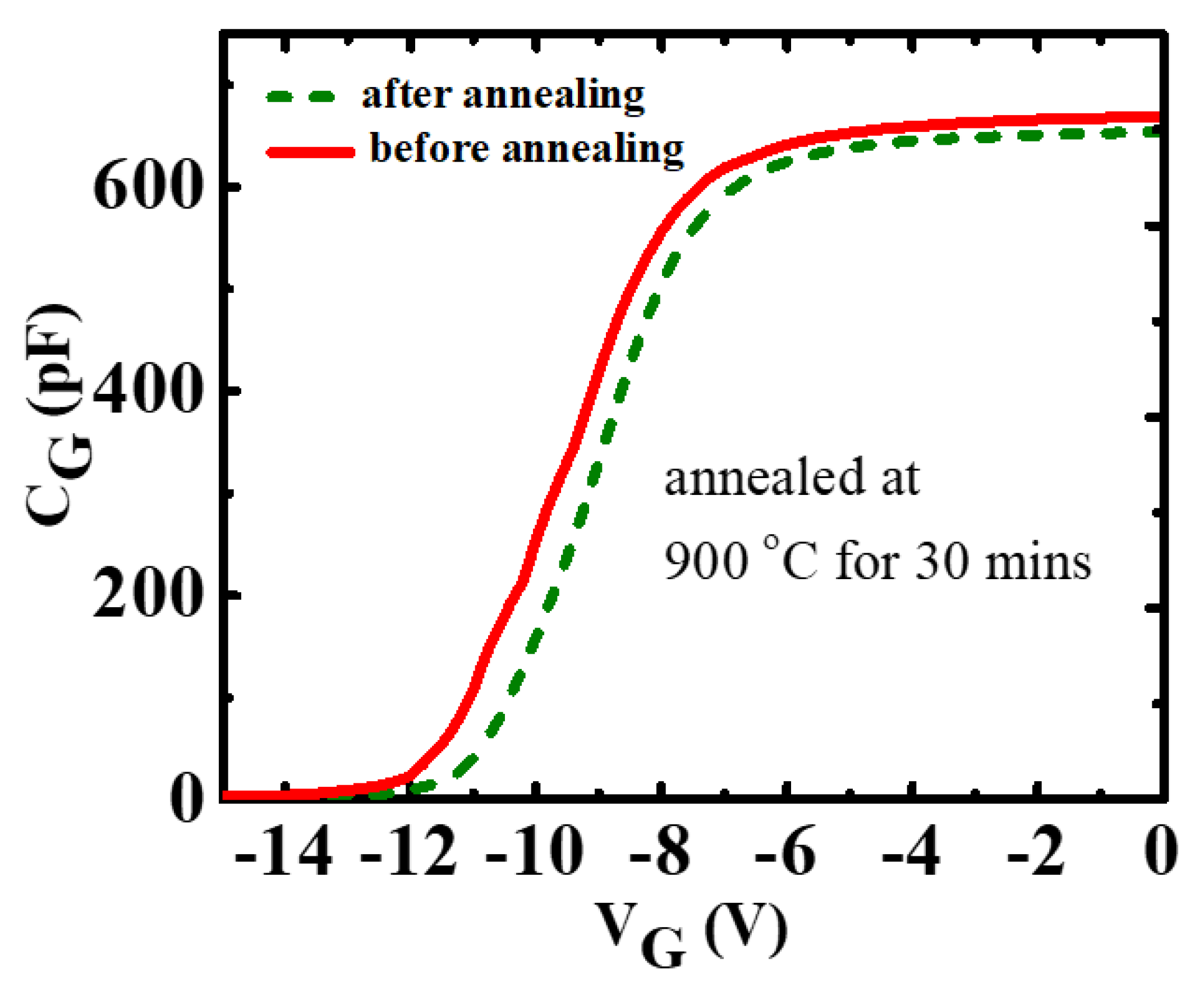
Figure 6.
2DEG carrier density in FETs vs. applied gate voltage for different gate oxide thicknesses.
Figure 6.
2DEG carrier density in FETs vs. applied gate voltage for different gate oxide thicknesses.
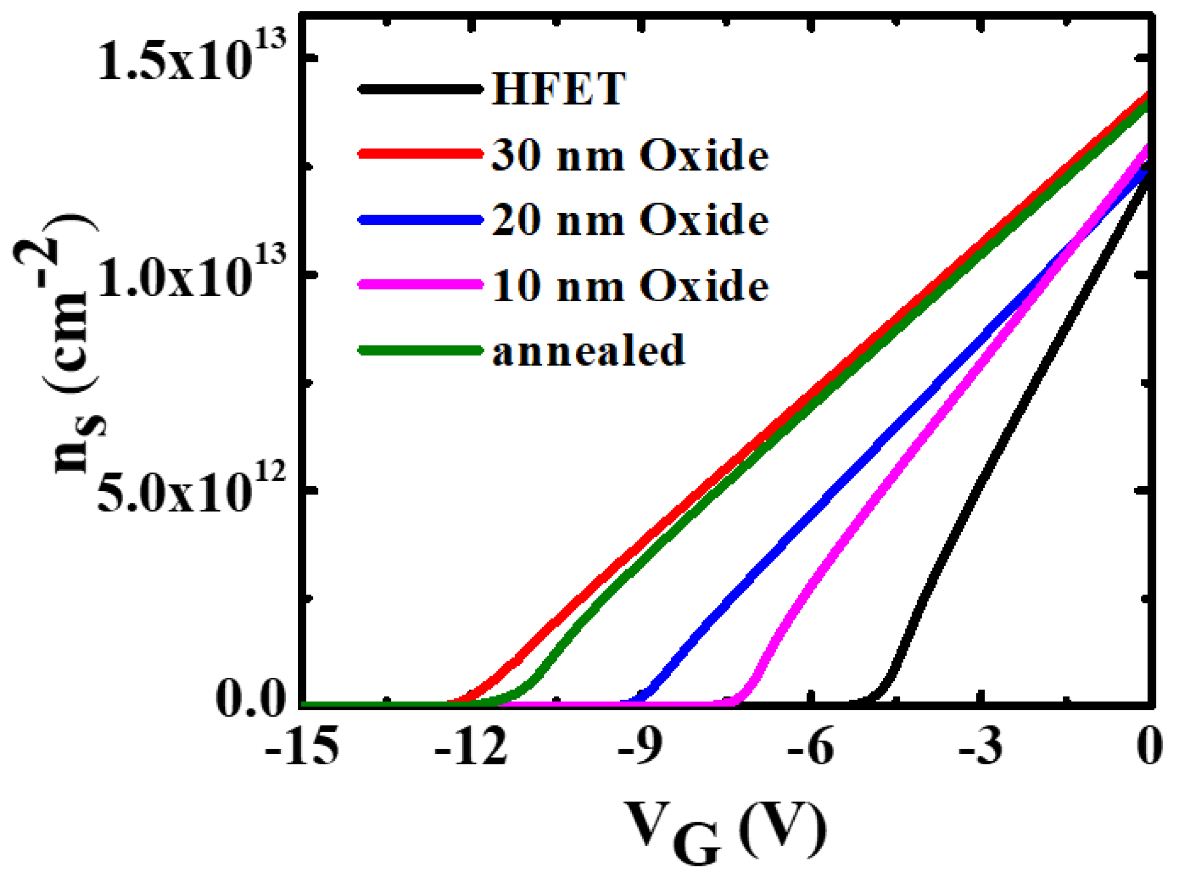
Figure 7.
Frequency-dependent C-V characteristic of a MOSHFET with 10 nm thick gate oxide at frequencies of 100 kHz, 316 kHz, and 1 MHz.
Figure 7.
Frequency-dependent C-V characteristic of a MOSHFET with 10 nm thick gate oxide at frequencies of 100 kHz, 316 kHz, and 1 MHz.

Disclaimer/Publisher’s Note: The statements, opinions and data contained in all publications are solely those of the individual author(s) and contributor(s) and not of MDPI and/or the editor(s). MDPI and/or the editor(s) disclaim responsibility for any injury to people or property resulting from any ideas, methods, instructions or products referred to in the content. |
© 2023 by the authors. Licensee MDPI, Basel, Switzerland. This article is an open access article distributed under the terms and conditions of the Creative Commons Attribution (CC BY) license (http://creativecommons.org/licenses/by/4.0/).
Copyright: This open access article is published under a Creative Commons CC BY 4.0 license, which permit the free download, distribution, and reuse, provided that the author and preprint are cited in any reuse.


