

Submitted:
09 February 2018
Posted:
11 February 2018
You are already at the latest version
Abstract
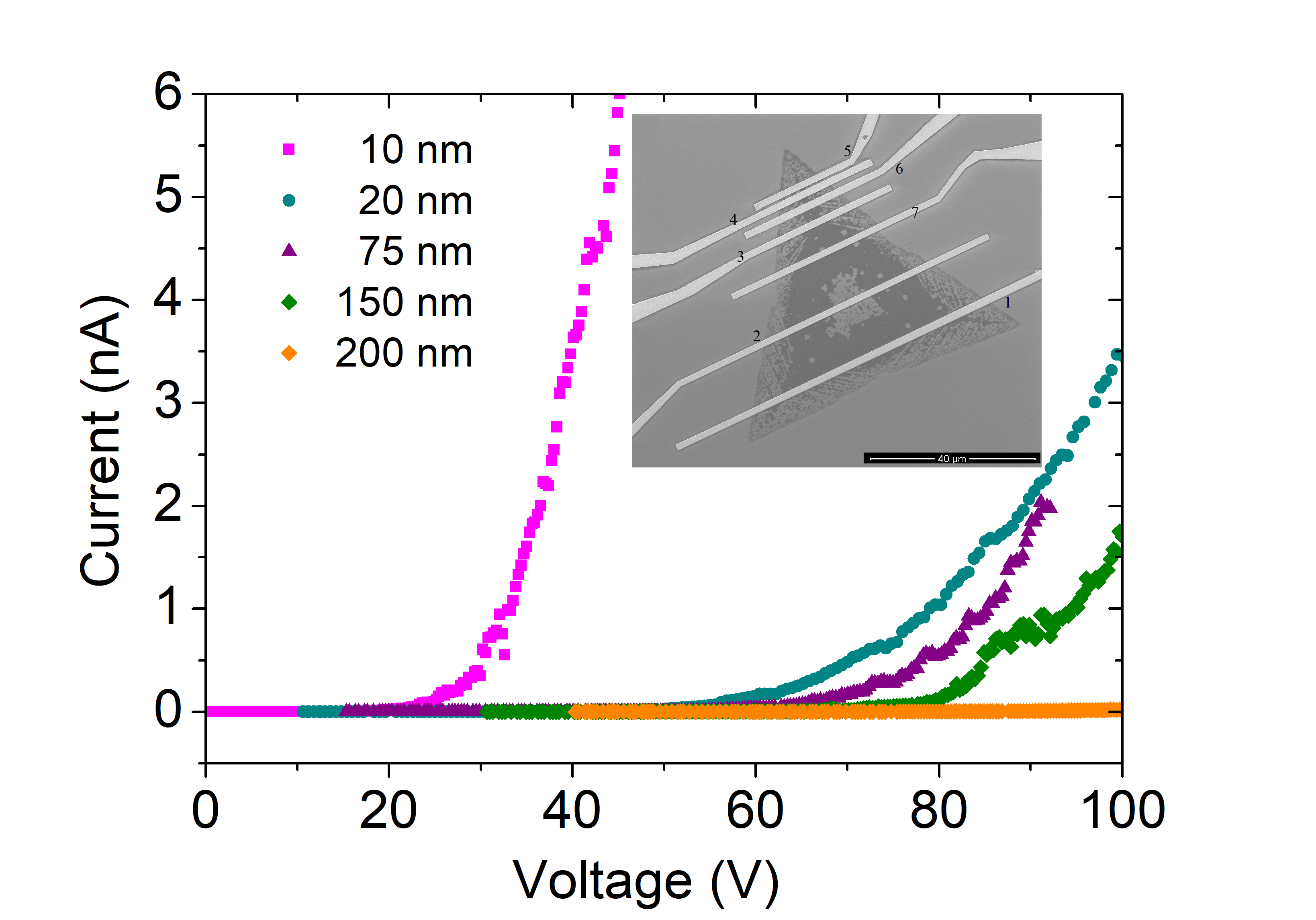
We report the electrical characterization and the field emission properties of CVD-grown MoS2 bilayers deposited on SiO2/Si substrate. Current-voltage characteristics are measured in the back-gate transistor configuration, with Ti contacts patterned by electron beam lithography. We confirm the n-type character of as-grown MoS2 and we report normally-on field effect transistors. Local characterization of field emission is performed inside a scanning electron microscope chamber with piezo-controlled tungsten tips working as the anode and the cathode. We demonstrate that an electric field of ~200 V/μm is able to extract current from the flat part of MoS2 bilayers, which therefore can be conveniently exploited for field emission applications even in low field-enhancement configurations. We show that a Fowler-Nordheim model, modified to account for electron confinement in 2D materials, fully describes the emission process.
Keywords:
transition metal dichalcogenides
; MoS2
; field effect transistor
; field emission
Copyright: This open access article is published under a Creative Commons CC BY 4.0 license, which permit the free download, distribution, and reuse, provided that the author and preprint are cited in any reuse.


