

Submitted:
17 November 2026
Posted:
18 November 2026
You are already at the latest version
Abstract
Polydimethylsiloxane (PDMS), a silicon-containing polymer, is widely used in flexible electronics, coatings, and polymer-derived ceramics. However, its response to high-intensity pulsed photonic processing under inert and reducing atmospheric environments remains insufficiently understood. Spin-coated PDMS films (~5 μm) were photonically cured using millisecond xenon-flash pulses at fluences up to 4.1 J/cm² and pressures up to 4 atm under argon (Ar), forming gas (5% H₂ in Ar), and vacuum. Fourier-transform infrared spectroscopy (FTIR), energy-dispersive X-ray spectroscopy (EDS), and scanning electron microscopy (SEM) evaluated chemical, compositional, and morphological changes. FTIR revealed reduced methyl-group signatures and siloxane bonding restructuring, particularly under forming gas. EDS indicated Si retention (19 wt% Si at 3 atm and 2.6 J/cm2) and enhanced carbon removal. Ar limited oxygen (O2) incorporation, whereas vacuum produced minor structural changes. SEM revealed relatively smooth film surfaces. The combined observations suggest the formation of disordered Si-rich, O2, and C containing nanostructures (SiOₓCᵧ). Within the investigated pressure range, 3 atm yielded the strongest observed structural transformation under forming gas. These findings demonstrate that atmosphere, pressure, and fluence jointly influence PDMS transformation. To the best of our knowledge, this is the first systematic investigation establishing a scalable, pressure-assisted pulse photonic processing route for PDMS-derived SiOₓCᵧ based nanostructure. Higher fluence, while maintaining 3 atm and improving oxidation control warrant further investigation for potential energy-storage applications.
Keywords:
photonic curing
; polydimethylsiloxane
; silicon oxycarbide
; thin films
; forming gas
; pressure-controlled processing
1. Introduction
Lithium-ion batteries (LIBs) have become the dominant energy storage technology due to their high gravimetric energy density, long cycle life, and relatively high operating voltage. For more than five decades, graphite has remained the commercial standard anode material in batteries, delivering a stable gravimetric energy capacity of approximately 372 mAh/g [1]. However, the ever-increasing demand for higher performance energy storage systems has driven extensive research toward alternative anode materials with higher capacity and improved energy density [2,3,4,5,6,7].
Among the proposed candidates, Si has attracted significant attention due its exceptionally high theoretical capacity, ranging from 3,579 mAh/g at room temperature to 4,212 mAh/g at elevated temperatures [8], which is more than ten times that of graphite which is the norm [1,8]. Together with other advantages, Si is abundant, low cost, and has low toxicity. These make it highly attractive for next generation LIBs. However, its practical implementation is severely limited by larger volume expansion (~300%) during lithiation and delithiation. This results in particle pulverization, unstable solid-electrolyte interphase formation, loss of electrical contact, and rapid capacity fading as well [5,6,7,8,9,10].
To address these challenges, multiple strategies have been explored. Nanostructuring Si into nanoparticles (NPs) has been widely adopted to accommodate mechanical strain and improve cycling stability [11]. In addition, SiC composite anodes have been developed to combine the high capacity of Si with the structural stability and electrical conductivity of C [12]. In these systems, C acts as both a conductive matrix and a mechanical buffer, mitigating the large volume expansion of Si and helping to maintain electrical connectivity during repeated lithiation and delithiation cycles [13]. However, the electrochemical performance of SiC composites highly depended on the Si content, where lower Si fractions improve structural stability at the expense of capacity, while higher Si loadings increase capacity but lead to greater mechanical degradation and loss of electrical contact [7,14].
More recently, covalent engineering approaches have been introduced, where Si is encapsulated within two-dimensional C frameworks through strong Si-O-C bonding, enhancing interfacial stability and maintaining continuous electron transport during cycling [15]. In addition, porous SiOₓCᵧ architectures have been developed to facilitate fast charge/discharge kinetics and buffer volume expansion [6,7,13]. Despite those advantages, achieving uniform Si dispersion and well-controlled architectures, such as core shell or embedded structures, requires sophisticated and complex multi-step synthesis processes. These challenges limit scalability, reproducibility in large scale manufacturing, ultimately increasing the cost of commercial lithium-ion batteries [6,10,12,16]. Furthermore, although SiC composites improve mechanical stability and conductivity, they still suffer from structural degradation, interfacial instability, reduced capacity (typically below 1,300 mAh/g), and slow lithium diffusion kinetics during prolonged cycling [13,14,17,18,19,20,21].
Germanium (Ge), another group IV element, offers faster lithium diffusion and moderate capacity of ~ 1,600 mAh/g. Notably, amorphous Ge nanoparticles exhibit improved cycling stability compared to crystalline counterparts due to more homogeneous volume expansion and reduced mechanical stress accumulation [22,23]. This behavior highlights the broader importance of amorphous phases in mitigating structural degradation in anode materials. However, Ge remains impractical for large-scale applications due to its high cost, limited abundance, and toxicity concerns [24,25,26].
More recently, MXenes, with a general formula of Mₙ₊₁XₙTₓ (where M is an early transition metal, X is carbon and/or nitrogen, and Tₓ represents surface terminations such as -O, -OH, -F, -Br, -I or -Cl), being two dimensional layered structure with larger surface area, high electrical conductivity and tunable surface chemistry [27,28], has emerged as promising materials for mitigating (to buffer) Si volume expansion due to its mechanical flexibility and hydrophilic nature that further enhances ion transport and interfacial stability [5,6,27,29]. The integration of MXenes with Si has shown significant improvements in electrochemical performance, capacity retention and cycling stability [6]. Dual-confinement strategies using MXenes and carbon frameworks promote strong interfacial bonding (e.g., Si-O-Ti and Si-C bonding), suppresses nanoparticle aggregation, enhance charge transfer kinetics (ion transport), and improved electrolyte accessibility, to accommodation of volume expansion during cycling [7,30]. Despite these advantages, MXene-based systems still face challenges such as restacking, oxidation sensitivity, and synthesis complexity [27]. Moreover, they do not fully eliminate Si major problem of volume expansion, and long-term stability remains dependent on interfacial design and composite architecture [5,7]. These limitations motivate the exploration of alternative strategies that can directly generate Si-rich structures with improved stability.
An alternative approach involves the use of Si-containing polymers as precursors for Si-based materials. Early studies demonstrated that pyrolysis of polysiloxanes produces Si oxycarbide (SiOₓCᵧ) amorphous materials with reversible capacities up to ~ 900 mAh/g [1,31]. These materials consist of disordered carbon domains embedded within an amorphous Si-O-C glass matrix, which enhances electronic conductivity, facilitates lithium transport, and improves structural stability at high temperature [32]. Despite these advantages, in addition to being time consuming, conventional pyrolysis requires high temperatures (≥1000°C), limiting compatibility with flexible substrates and scalable processing. Furthermore, these processes predominantly yield Si-O-C phases rather than pure Si nanoparticles, making it difficult to fully utilize the Si’s theoretical capacity. In parallel, metallothermic reduction of silica have been explored to produce porous Si nanostructures at relatively moderate temperatures (typically 450 - 800°C) using reductants such as Mg or Al [8,33]. While these approaches offer scalability and cost advantages, they often result in structural damage, morphology changes, or require additional post-processing steps, limiting precise control over the final nanostructure and composition.
Photonic PulseForge curing processing has recently emerged as a promising alternative for rapid transformation of polymer-derived materials [24,34]. This technique utilizes intense broadband light pulses (200 – 1100 nm) from a xenon flashlamp to deliver high energy densities within microsecond to millisecond timescales, enabling rapid, localized heating of thin films without significant bulk heating of the substrate [22,35,36,37]. Such characteristics make photonic curing particularly attractive for processing (or enable fast modifications in) thin films on temperature-sensitive and flexible substrates.
PDMS is an organosilicon polymer widely used in coatings, microfluidics, flexible electronics, sensors, biomedical devices, paints, glues, and optoelectronic applications due to its excellent thermal stability, chemical resistance, flexibility, non-toxicity, gas permeability, optical transparency in the visible range, corrosion resistance, biocompatibility, high dielectric constant, and strong adhesion properties [3,11,17,38,39,40,41,42]. More recently, PDMS was also proposed as a precursor (or intercalant) for Si-based nanostructures confined into MXene layers for energy applications [9]. However, there have been no preliminary studies which prove that one can synthesize SiNPs from PDMS under high-intense photonic curing processing conditions. Furthermore, PDMS undergoes complex degradation pathways, including depolymerization into cyclic siloxanes under reducing conditions or thermo-oxidative degradation leading to the formation of SiO2 and volatile species such as CO2 and H2O [43,44]. These mechanisms highlight the importance of precisely controlling processing conditions (such as atmosphere, pressure, fluence, exposure time, frequency rate, and the number of counts) to tailor the resulting material composition and structure [44,45,46,47]. In addition to this, a detailed study/investigation of pulse light interaction with materials via PulseForge is imperative to understand and implement photonic curing process [9].
Photonic curing system presents intrinsic limitations. Its processing capacity depends strongly on film’s thickness, typically < 50 µm [48] and energy distribution within polymeric, as well as layered systems [35,37,49]. In addition to these, its light penetration follows Lambert’s law, which is I = I0e−αl, with;
- I0 is the initial light intensity before entering the film (maximum intensity falling on the top of the film)
- I is transmitted light intensity after traveling through film
- α is the absorption coefficient of the film
- l is the distance or thickness traveled by the light inside the film
These, in addition to the flashpoint of PDMS which is ≈ 300˚C [43], create the following critical questions:
- (i)
- How do fluence and pressure influence bond breaking in PDMS, particularly Si-O-Si scission and methyl group removal?
- (ii)
- How do environments (reducing, inert, or vacuum) affect carbon removal and Si phase formation?
- (iii)
- Can photonic curing accelerate the kinetics of crystalline Si-carbon nanoparticle growth, and under what conditions can it yield novel SiC or SiOₓCᵧ structures?
In this work, we introduce a photonic curing strategy to investigate the transformation of thin spin coated PDMS films (~ 5 µm) under systematically controlled environments, including forming gas (5% H₂ in Ar), Ar, and vacuum. By varying fluence and pressure, we examine their combined effects on PDMS decomposition pathways and SiCx formation. In addition to enabling rapid, localized energy delivery, photonic curing offers a potentially energy-efficient and scalable alternative to conventional multi-step synthesis routes, thereby reducing processing complexity and manufacturing cost [37,38]. We hypothesize that:
- (i)
- Under identical photonic curing conditions, gas composition governs PDMS decomposition pathways and final composition. forming gas enhances carbon removal and promotes Si-rich phase formation, Ar limits oxidation but preserves less Si, while vacuum induces minimal structural change;
- (ii)
- Under identical atmospheric conditions, increasing fluence and pressure intensifies bond scission, thereby accelerating PDMS degradation and driving the formation of SiC amorphous phases.
Our results demonstrate that photonic curing transforms PDMS from chemically stable precursor into a reactive source of Si rich amorphous nanostructures. The resulting SiOₓCᵧ phases can exhibit improved structural adaptability, reduced stress accumulation, and more isotropic lithium diffusion, thereby enhancing stability during electrochemical cycling [1,12,31,32]. This study establishes a multi-parameter framework for understanding the role of gas composition, fluence, and pressure in photonic processing of polymer-derived materials and provides a scalable pathway for synthesizing Si-based nanostructures on flexible substrates for next-generation energy storage applications. The structural and compositional changes were analyzed using FTIR, EDS, and SEM.
2. Materials and Methods
2.1. Materials and Film Preparation
PDMS, bis(3-aminopropyl)-terminated (-[Si(CH3)2-O]n-, density 0.98 gm/L at 25°C; Sigma-Aldrich) was diluted in toluene (LabChem, 100%) at a 1:1 mass ratio. The mixture was homogenized using a magnetic hotplate stirrer (SCILOGEX MS – H280 – Pro) for 60 minutes [50,51], and the spin coating was selected to ensure uniform film thickness and reproducibility [19,25,52]. Copper (Cu) substrates were ultrasonically cleaned in acetone, ethanol, and deionized water (10 min each, using Bransonic CPX2800H) and dried under compressed air [4,9,19,36]. The PDMS-toluene solution was spin-coated using a Laurell WS-650 Lite system at 500 rpm for 5 s and then 4,000 rpm for 30 s, yielding ~ 5 μm films. Thickness estimates were obtained using the empirical spin-coating relationship [19,25,52,53].
2.2. Photonic Curing
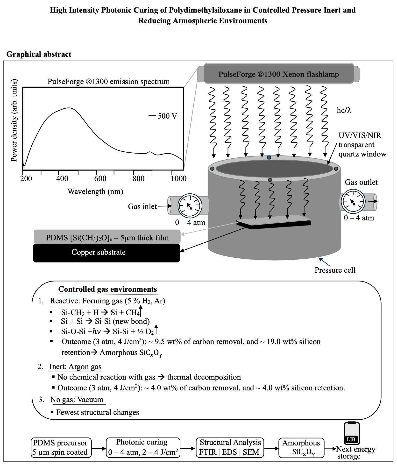
Films were dried at room temperature for 48 h prior to curing. Photonic processing was then performed in pressure-controlled vacuum chamber [54] via PulseForge® 1300 in vacuum and forming gas and Ar environments. The PulseForge is photonic curing system with a rapid thermal processing technique that uses high intensity, short-duration xenon flash pulse trains with broadband emission spanning from 200 – 1100 nm [36], to selectively heat thin films to high temperatures while minimizing heat transfer to the underlying low-temperature substrate, thereby enabling annealing or other thermally activated processes without substrate damage [36,37,48].
forming gas was purchased from Airgas USA LLC containing actual concentration of 4.985 +/- 2 % of H₂ in Ar gas. Processing pressures ranged from 2 to 4 atm. The photonic curing parameters are outlined in the Table 1. The fluence reported is measured through bolometer [24]. Spin coating was chosen over spray coating to have uniform film, and to facilitate the uniform dispersion of energy density during processing [50,52]. The schematics of the photonic curing and experiment is shown is Figure 1 and Figure 2. Increasing the discharge voltage uniformly increases the xenon-flash intensity without substantially changing the overall spectral shape [36]. The 5% H₂ concentration in forming gas was chosen to balance reducing capability, safety, and cost-effectiveness while remaining below hydrogen flammability limits in air [20].
2.3. Characterization
FTIR spectra were collected with a Nicolet iS10 spectrometer (130 W, +12 V) to track functional group changes. Elemental analysis was performed using an EDS (INCA–Hitachi S-3400 system at 30 kV). Stoichiometric calculations were compared with measured compositions to quantify Si, C, and O2 changes. Surface morphology was imaged with SEM (a Hitachi S-4800 at 20 kV). Prior to imaging, samples were carbon-coated (using Cressington coater) to enhance conductivity.
3. Results
3.1. FTIR Results
FTIR spectra show that photonic curing modifies the PDMS structure depending on gas environment, fluence and pressure. FTIR of two sets of experiments was measured. In first set, the fluence and chamber pressure were held constant while the processing atmosphere was varied (Figure 3). Uncured PDMS spectrum contains characteristic bands near 1257, 1010, 791, and 698 cm-1, assigned to Si-CH₃ deformation, Si-O-Si stretching, Si-C/CH₃-related vibrations, and Si-rich SiOₓCᵧ, respectively. After curing, changes in the normalized intensities and shapes of these characteristic bands indicate modification of PDMS chemical structure.
Comparing the FTIR peaks of cured and uncured PDMS, the Si-CH₃ related peak at 1257 cm-1 stayed sharp, but with a significant drop in intensity. These changes are particularly evident under forming gas at 3 atm and 4.08 J/cm2. The decrease in the Si-CH₃ vibration, indicating methyl group removal and partial decomposition of the PDMS side groups during photonic processing [55]. The changes in the low-wavenumber below 791 cm-1 (of figure 3) indicate modification of the local Si-C/Si-O bonding and suggest the formation of Si-rich, sub-stoichiometric SiOₓ/SiCₓOᵧ species [2,22,56].
The Si-O-Si region around 1010 cm⁻¹ also changes strongly after curing, especially under forming gas. Although the characteristic Si-O-Si band near 1010 cm⁻¹ remains present after curing, its intensity and spectral shape are modified. This indicates restructuring of the siloxane backbone and possible conversion of the original PDMS network into a more disordered Si-O-C/SiCₓOᵧ matrix [55], while symmetric stretches at 791 cm-1 indicates Si-C species [57,58]. So, the strongest transformation occurred in forming gas at 3 atm and 4.08 J cm-2 suggests an extensive PDMS decomposition, methyl removal, and backbone restructuring. The corresponding compositional results (EDS) in Figure 5, show greater Si retention accompanied by C removal under forming gas, to further support the FTIR evidence for transformation toward a more Si-rich material.
A comparison between figures 3(c) and 3(d) further reveals two more important things. One is that the spectral changes are most pronounced in forming gas, particularly at 3 atm and 4.08 J/cm², where the strong decrease of characteristic PDMS bands suggests enhanced bond scission, volatile fragment removal, and formation of new Si-rich species [2,22,35]. The strength of forming gas is indicated in figure 5, where more Si retention, and C removal became high in forming gas. The second very important thing is the pressure dependance. At the same fluence of 4.08 J/cm², forming gas spectrum obtained at 4 atm exhibits less pronounced modifications that what obtained at 3 atm in both forming gas and Ar environments (figure 5). This indicates that increasing pressure beyond 3 atm did not further enhance decomposition. Therefore, increasing pressure beyond 3 atm does not necessarily enhance PDMS conversion. This suggests that PDMS transformation depends on an optimum condition of high fluence, the choice of flowing gas in the chamber, with 3 atm as an optimum pressure.
In the second set of experiments, the processing gas was held constant while PulseForge tube voltage and chamber pressure were varied (Figure 4). Ar-treated samples showed moderate and inconsistent changes (figure 4 (a), and figure 5). The Si-CH₃ band decreases, and the Si-O-Si region is modified. While these still indicate partial decomposition and restructuring of PDMS network, the transformation is generally weaker than in forming gas. Vacuum-treated samples exhibited comparatively smaller spectral changes, suggesting limited PDMS decomposition under the same investigated photonic curing conditions.
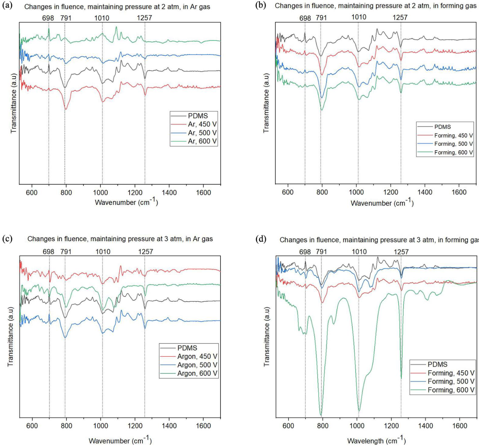
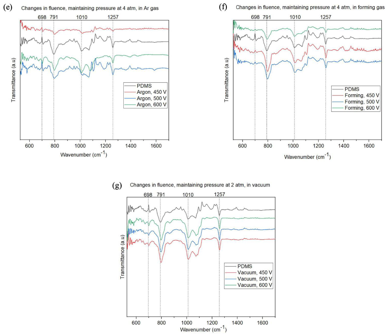
Figure 4.
Si formation and C removal efficiency vary with atmospheric pressure and applied fluence (voltage), with 3 atm identified as the optimum processing pressure.
Figure 4.
Si formation and C removal efficiency vary with atmospheric pressure and applied fluence (voltage), with 3 atm identified as the optimum processing pressure.
The combined normalized FTIR analysis (of the two sets) further demonstrated that PDMS conversion during photonic curing is controlled by the combined effects of incident fluence, pressure, and gas environment. forming gas was the most effective environment for both C removal and Si retention, consistent with hydrogen-assisted decomposition pathways in which H₂ promotes Si-CH₃ bond cleavage and volatilization of hydrocarbon species, thereby enriching the remaining Si-containing matrix [20,43,44]. Our results show that increasing fluence at optimum pressure (3 atm) further intensified PDMS decomposition. This in turn, supports the hypothesis that higher energy densities accelerate Si-O-Si backbone scission, PDMS restructuring, and carbon volatilization.
This study was limited to fluences of 2 – 4.1 J/cm²; however, the observed trends suggest that increasing the fluence further, for example 8 – 12 J/cm² under forming-gas maintained at 3 atm, would intensify Si-O-Si bond scission, enhance C volatilization, and promote greater Si enrichment. Nevertheless, higher fluence alone should not be expected to fully suppress oxygen incorporation. Instead, stronger pulsed heating would likely accelerate volatilization of organic fragments and promote formation of more porous amorphous Si-rich SiC structures through enhanced gas evolution and transient local heating [43,44,46,47].
3.2. EDS Results
To contextualize the EDS results, stoichiometry was calculated for Spin-coated PDMS films (C₂H₆OSi, density 0.98 g/cm³, ~ 5.0 ± 0.1 μm thick at 5000 rpm, consistent with reported scaling laws) [19]. Each 1 cm² film contained ~ 490 μg of PDMS, equivalent to 183.8 μg of Si, 157.1 μg of carbon, 104.6 μg of oxygen, and 39.5 μg hydrogen.
EDS confirmed the FTIR observations. Forming gas consistently promoted carbon removal and Si retention, especially at higher fluences and pressures (Figure 5). Under forming gas (at 3 atm), maximum values reached ~ 19.0 wt% Si, with ~ 9.5 wt% relative carbon loss, compared with ~ 4.0 % Si and < 2.0 % carbon loss in Argon (figure 6). Vacuum curing showed a minimal PDMS decomposition (figures 4 and 5), consistent with the limited structural modifications observed in FTIR spectra. Unexpectedly, Argon processing (3 atm, 4.1 J/cm2) introduced less oxygen incorporation (~ 5.0 wt%) than forming gas (~ 10 wt%), suggesting incomplete reduction by H₂ or residual oxygen contamination (figure 5). Due to this significant oxygen incorporation, stoichiometric analysis was further used to clarify the role of hydrogen during photonic curing. For a 5 μm PDMS film containing approximately 2.4 × 10¹⁹ H atoms and 4 × 10¹⁸ O atoms, the forming-gas environment contributed ~2.5 × 10²¹ H₂ molecules and 4.7 × 10²² Ar molecules at 3 atm, indicating that hydrogen availability was sufficient to influence oxygen-containing species during transient photonic processing. Nevertheless, increasing the H₂ concentration substantially beyond 5% was not considered because hydrogen flammability in air becomes significant near ~ 4%, thereby increasing safety concerns during high-fluence pulsed irradiation [20,42,59]. These observations indicate that although forming gas enhanced carbon volatilization and Si retention, oxygen incorporation remained difficult to fully suppress under the present experimental conditions.
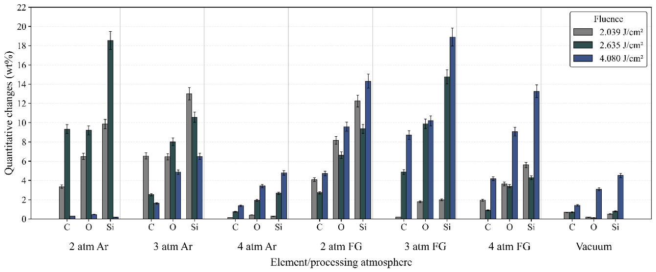
Figure 5.
EDS results showing the quantitative changes in photonically cured PDMS films processed under vacuum, argon, and forming gas (FG) at different pressures and fluences. (a) Relative carbon content, showing carbon removal during photonic curing. (b) Relative oxygen content, showing oxygen incorporation under different atmospheric environments. (c) Relative Si content, demonstrating Si enrichment after photonic processing.
Figure 5.
EDS results showing the quantitative changes in photonically cured PDMS films processed under vacuum, argon, and forming gas (FG) at different pressures and fluences. (a) Relative carbon content, showing carbon removal during photonic curing. (b) Relative oxygen content, showing oxygen incorporation under different atmospheric environments. (c) Relative Si content, demonstrating Si enrichment after photonic processing.
3.3. SEM Results
The SEM imaging revealed a relatively smooth surface morphology, together with isolated granular white features (figure 6 (a)), one of which is shown at higher resolution in figure 6(b). The smooth morphology together with the uniform elemental distribution (EDS mapping showing the elemental distribution of Si, C, and O throughout the cured films, figure 6 (c – f)) suggests the formation of amorphous SiCₓOᵧ species rather than large segregated crystalline phases. These results suggest that the photonic curing produced amorphous SiC, despite oxygen species which may be related to the post-treatment oxidation [47].
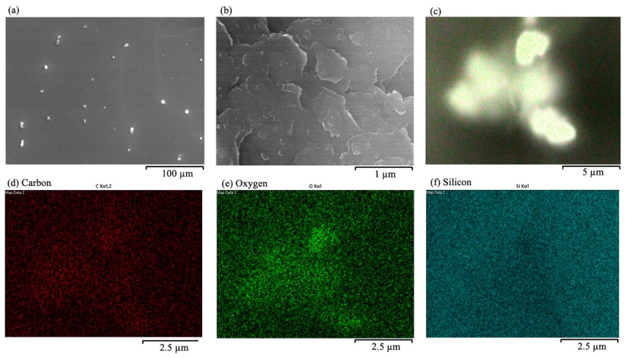
Figure 6.
SEM images and EDS elemental maps of photonically cured PDMS. (a) Low-magnification SEM image showing the overall film morphology and isolated white spots distributed across the surface. (b) SEM image of one of the white spots at high resolution. (c): Enlarged EDS map selected for elemental mapping, to show how Si, C and O2 are uniformly distributed in SEM image. (d) Carbon elemental distribution. (e) Oxygen elemental distribution. (f) Si elemental distribution.
Figure 6.
SEM images and EDS elemental maps of photonically cured PDMS. (a) Low-magnification SEM image showing the overall film morphology and isolated white spots distributed across the surface. (b) SEM image of one of the white spots at high resolution. (c): Enlarged EDS map selected for elemental mapping, to show how Si, C and O2 are uniformly distributed in SEM image. (d) Carbon elemental distribution. (e) Oxygen elemental distribution. (f) Si elemental distribution.
The broad FTIR features (Figure 2 and Figure 3) together with the uniform EDS elemental distribution (Figure 5(c–f)), indicate that Si-rich species were dispersed within a disordered PDMS-derived matrix rather than forming long-range crystalline structures. This behavior is consistent with ultrafast non-equilibrium photonic processing, where millisecond thermal exposure limits long-range atomic diffusion and promotes kinetically trapped structures [34,37]. In addition, the relatively high oxygen content, even under forming gas, likely stabilized Si-O bonding and further favored retention of the amorphous Si-rich Si-C-O network [31,32].
Consistent with this interpretation, SEM did not reveal distinct crystalline Si nanoparticles (Figure 7a), even though FTIR showed Si-Si bond signatures and EDS confirmed elevated Si content. Taken together, these observations support the formation of amorphous Si-rich SiCₓOᵧ nanostructures during photonic curing [2,8,60]. At sufficiently high local temperatures (T > 1,000˚C) and longer time (500 µm < t ≤ 2500 µm, see figure 3), partial semi-crystalline SiC or Si-rich nanodomains could eventually nucleate. Fully crystalline SiC, however, may not be desirable for energy-storage (lithium-ion batteries) applications because amorphous SiC can provide greater structural adaptability, improved strain accommodation, and enhanced resistance to fracture during lithiation/delithiation cycling [1,12,15,18,31,32,40,61]. Consequently, oxygen-free processing conditions, improved chamber isolation, vacuum transfer, in situ capping layers, rapid encapsulation, or co-deposition of conductive carbon precursors may help suppress post-treatment oxidation and promote formation of more stable amorphous Si-rich SiCₓ structures. Therefore, the amorphous Si-O-C/SiCₓ nanostructures derived from PDMS in this work hold promise for lithium-ion battery applications, and complement the work reported by Synthesis and photothermal processing of Si-based nanoconfined MXenes (Khatoon et al., 2025) [9].
5. Conclusions
Pulsed photonic curing induced significant chemical and structural transformation of PDMS under forming gas, Argon, and vacuum environments. In all cases, pulsed photonic excitation promoted Si-O-Si bond scission, methyl-group removal, carbon volatilization, and Si enrichment. Forming gas accelerated carbon depletion and produced the highest Si retention, whereas Argon more effectively suppressed oxygen incorporation. Vacuum processing induced the fewest structural changes overall. FTIR, EDS, and SEM collectively indicated Si-rich phase evolution, supporting the formation of amorphous Si-rich SiCₓOᵧ nanostructures generated through ultrafast photonic curing of PDMS. The resulting amorphous Si-rich Si-C-O networks may provide improved structural adaptability, reduced stress accumulation, and enhance stability for lithium-ion battery applications. This study therefore establishes a scalable and substrate-compatible framework for photonic synthesis of PDMS-derived Si-based nanostructures for next-generation energy-storage systems. This study establishes a scalable, substrate-compatible, and energy-efficient framework for photonic synthesis of PDMS-derived Si-based nanostructures under controlled-pressure environments, providing new opportunities for next-generation energy-storage and flexible electronic materials.
Supplementary Materials
The supporting information submitted with this manuscript will be made available online by the publisher upon publication of the article.
Author Contributions
- Jean Paul Hagumimana: Conceptualization, methodology, investigation, data interpretation, and formal analysis, writing of the original draft.
- Najma Khatoon: Scientific discussion, manuscript review and editing.
- Sepideh Khalili: Experimental support and manuscript review.
- Simon Oppong Asare: Manuscript review and discussion.
- Keyuan Bai: Manuscript review and discussion
- Sunil Pokhrel: Manuscript review and discussion
- Douglas B. Chrisey: Supervision, funding acquisition, project administration, writing – review and editing.
Funding
This work was supported by Tulane University through research support provided within the Department of Physics and Engineering Physics. We acknowledge graduate research support under the supervision of Prof. Douglas B. Chrisey.
Data Availability Statement
The data supporting the findings of this study are included in the article and its Supplementary Materials. Additional data are available from the corresponding author upon reasonable request.
Acknowledgments
We thank the facilities and research environment provided by the department of Physics and Engineering of Tulane University, for their continuous support of my academic work.
Conflicts of Interest
The authors declare that they have no known competing financial interests or personal relationships that could have appeared to influence the work reported in this paper.
References
- Xing, W.; et al. Pyrolyzed polysiloxanes for use as anode materials in lithium-ion batteries . J. Electrochem. Soc. 1997, 144(7), 2410–2416. [Google Scholar] [CrossRef]
- Anbarasan, P.; et al. Spectral and morphological studies of nanocrystalline silicon thin films synthesized by PECVD for solar cells . Silicon 2010, 2(1), 7–17. [Google Scholar] [CrossRef]
- Ariati, R.; et al. Polydimethylsiloxane composites characterization and its applications: a review . Polymers 2021, 13(23), 4258. [Google Scholar] [CrossRef] [PubMed]
- Bourgeois, B.B.; et al. Pulsed photonic fabrication of nanostructured metal oxide thin films . Appl. Phys. A 2017, 123(9), 588. [Google Scholar] [CrossRef]
- Jiang, X.; et al. Recent progress in Si/Ti3C2Tx MXene anode materials for lithium-ion batteries . IScience 2024, 27(11). [Google Scholar] [CrossRef] [PubMed]
- Li, X.; et al. Three-dimensional hierarchical porous structures constructed by two-stage MXene-wrapped Si nanoparticles for Li-ion batteries . ACS Appl. Mater. Interfaces 2020, 12(43), 48718–48728. [Google Scholar] [CrossRef] [PubMed]
- Zhang, X.; et al. Strategies for controlling or releasing the influence due to the volume expansion of silicon inside Si− C composite anode for high-performance lithium-ion batteries . Materials 2022, 15(12), 4264. [Google Scholar] [CrossRef] [PubMed]
- Lee, J.H.; et al. Polysiloxane-derived silicon nanoparticles for Li-ion battery . J. Energy Storage 2020, 27, 101141. [Google Scholar] [CrossRef]
- Khatoon, N.; et al. Synthesis and photothermal processing of silicon-based nanoconfined MXenes . Adv. Mater. Interfaces 2025, 12(8), 2400447. [Google Scholar] [CrossRef]
- Park, I.; Lee, H.; Chae, O.B. Synthesis methods of Si/C composite materials for lithium-ion batteries . Batteries 2024, 10(11), 381. [Google Scholar] [CrossRef]
- Carneiro, J.; et al. A microparticle blood analogue suspension matching blood rheology . Soft Matter 2021, 17(14), 3963–3974. [Google Scholar] [CrossRef] [PubMed]
- Li, Z.; et al. Bridging porous Si–C composites with conducting agents for improving battery cycle life . J. Power Sources 2015, 286, 534–539. [Google Scholar] [CrossRef]
- Sujith, R.; et al. A review of silicon oxycarbide ceramics as next generation anode materials for lithium-ion batteries and other electrochemical applications . J. Mater. Chem. A 2023, 11(38), 20324–20348. [Google Scholar] [CrossRef]
- Larkin, R.-J.; Willenberg, S.C.; Ross, N. Silicon-based anodes towards enhanced cycling efficiencies for next-generation lithium-ion batteries . Int. J. Electrochem. Sci. 2023, 18(6), 100158. [Google Scholar] [CrossRef]
- Zhang, X.; et al. Stable high-capacity and high-rate silicon-based lithium battery anodes upon two-dimensional covalent encapsulation . Nat. Commun. 2020, 11(1), 3826. [Google Scholar] [CrossRef] [PubMed]
- Khan, M.I.; et al. Advantages and disadvantages of lithium-ion batteries, in Nanostructured Lithium-ion Battery Materials; Elsevier, 2025; pp. 47–64. [Google Scholar]
- Félix, A.S.C.; et al. Physical-chemical properties of PDMS samples used in tunable lenses . Intl. J. Eng. Sci. Innov. Tech 2014, 3, 563–571. [Google Scholar]
- Jia, H.; et al. Novel three-dimensional mesoporous silicon for high power lithium-ion battery anode material . Adv. Energy Mater. 2011. [Google Scholar] [CrossRef]
- Jiang, Y.; et al. New insights into spin coating of polymer thin films in both wetting and nonwetting regimes . Langmuir 2022, 38(41), 12702–12710. [Google Scholar] [CrossRef] [PubMed]
- Jo, Y.D.; Crowl, D.A. Explosion characteristics of hydrogen-air mixtures in a spherical vessel . Process Saf. Prog. 2010, 29(3), 216–223. [Google Scholar] [CrossRef]
- Zhang, P.; et al. Dual confinement of Si nanoparticles in a MXene/ZIF-8-derived carbon framework for lithium-ion batteries . ACS Appl. Nano Mater. 2022, 5(9), 12720–12728. [Google Scholar] [CrossRef]
- Lee, J.H.; et al. Rapid mold-free fabrication of long functional PDMS fibers . NPG Asia Mater. 2022, 14(1), 13. [Google Scholar] [CrossRef]
- Mishra, K.; et al. Porous germanium enabled high areal capacity anode for lithium-ion batteries . Compos. Part B Eng. 2019, 163, 158–164. [Google Scholar] [CrossRef]
- Khatoon, N.; Subedi, B.; Chrisey, D.B. Synthesis of silicon and germanium oxide nanostructures via photonic curing; a facile approach to scale up fabrication . ChemistryOpen 2024, 13(7), e202300260. [Google Scholar] [CrossRef] [PubMed]
- Koschwanez, J.H.; Carlson, R.H.; Meldrum, D.R. Thin PDMS films using long spin times or tert-butyl alcohol as a solvent . PLoS ONE 2009, 4(2), e4572. [Google Scholar] [CrossRef] [PubMed]
- Lee, H.; et al. Surface-stabilized amorphous germanium nanoparticles for lithium-storage material . J. Phys. Chem. B 2005, 109(44), 20719–20723. [Google Scholar] [CrossRef] [PubMed]
- Lim, K.R.G.; et al. Fundamentals of MXene synthesis . Nat. Synth. 2022, 1(8), 601–614. [Google Scholar] [CrossRef]
- Naguib, M.; et al. Two-dimensional nanocrystals produced by exfoliation of Ti3AlC2, in MXenes; Jenny Stanford Publishing, 2023; pp. 15–29. [Google Scholar]
- Lukatskaya, M.R.; et al. Ultra-high-rate pseudocapacitive energy storage in two-dimensional transition metal carbides, in MXenes; Jenny Stanford Publishing, 2023; pp. 723–743. [Google Scholar]
- Raj, S.K.; et al. MXene-nanoflower composites as high-performance electrode materials toward solid-state lithium-ion batteries . Next Energy 2025, 100421. [Google Scholar] [CrossRef]
- Laidani, N.B.; Sorarù, G.D. N-doped polymer-derived Si (N) OC: The role of the N-containing precursor . J. Mater. Res. 2015, 30(6), 770–781. [Google Scholar] [CrossRef]
- Ridley, M.J.; et al. Oxidation performance and limitations of additively manufactured SiC/Si─ O─ C composites at elevated temperatures . J. Am. Ceram. Soc. 2024, 107(1), 439–449. [Google Scholar] [CrossRef]
- Lai, Y.; Thompson, J.R.; Dasog, M. Metallothermic reduction of silica nanoparticles to porous silicon for drug delivery using new and existing reductants . Chemistry–A Eur. J. 2018, 24(31), 7913–7920. [Google Scholar] [CrossRef] [PubMed]
- de Boode, B.; et al. Glassy carbon manufacture using rapid photonic curing . J. Mater. Sci. 2022, 57(1), 299–310. [Google Scholar] [CrossRef]
- Farnsworth, S.; et al. The photonic curing process for printed electronics with applications to printed RFID tags and thin film transistors . NIP & Digital Fabrication Conference, 2012; Society of Imaging Science and Technology. [Google Scholar]
- Luo, S.; et al. Instantaneous photoinitiated synthesis and rapid pulsed photothermal treatment of three-dimensional nanostructured TiO2 thin films through pulsed light irradiation . J. Mater. Res. 2017, 32(9), 1701–1709. [Google Scholar] [CrossRef]
- Schroder, K.A. The photonic curing revolution: high-temperature processing on low-temperature materials; PULSEFORGE, INC.: Link, 2022. [Google Scholar]
- Cauchy-Clerc, H.; et al. Photonic curing for in-mold electronics . 9th Smart Plastics Congress, 2024. [Google Scholar]
- Chen, D.; et al. Thermal stability, mechanical and optical properties of novel addition cured PDMS composites with nano-silica sol and MQ silicone resin . Compos. Sci. Technol. 2015, 117, 307–314. [Google Scholar] [CrossRef]
- Shen, J.; et al. 4, 5-difluoro-1, 3-dioxolan-2-one as an film forming additive on LiNi0. 8Co0. 15Al0. 05O2/SiO@ C full cells . J. Electroanal. Chem. 2019, 834, 1–7. [Google Scholar]
- Sosnin, I.M.; Vlassov, S.; Dorogin, L.M. Application of polydimethylsiloxane in photocatalyst composite materials: A review . React. Funct. Polym. 2021, 158, 104781. [Google Scholar] [CrossRef]
- Wolf, M.P.; Salieb-Beugelaar, G.B.; Hunziker, P. PDMS with designer functionalities—Properties, modifications strategies, and applications . Prog. Polym. Sci. 2018, 83, 97–134. [Google Scholar] [CrossRef]
- Protsak, I.; et al. Thermogravimetric analysis of silicas chemically modified with products of deoligomerization of polydimethylsiloxane . J. Therm. Anal. Calorim. 2015, 121(2), 547–557. [Google Scholar] [CrossRef]
- Tasić, A.; et al. Synthesis, structure and thermogravimetric analysis of alpha, omega-telechelic polydimethylsiloxanes of low molecular weight . J. Serbian Chem. Soc. 2017, 82(12), 1395–1416. [Google Scholar] [CrossRef]
- Kubicka, M.; et al. Electrochemical properties and structure evolution of starch-based carbon nanomaterials as Li-ion anodes with regard to thermal treatment . Polymers 2019, 11(9), 1527. [Google Scholar] [CrossRef] [PubMed]
- Rau, A.V.; Lu, K. Self-etching Ti3C2Tx-SiOC ceramics: effects of MXene surface terminations on high-temperature ceramic nanocomposites . Adv. Compos. Hybrid. Mater. 2025, 8(3), 253. [Google Scholar] [CrossRef]
- Thu, M.M.; et al. Introducing micropores into carbon nanoparticles synthesized via a solution plasma process by thermal treatment and their charge storage properties in supercapacitors . RSC Adv. 2023, 13(24), 16136–16144. [Google Scholar] [CrossRef] [PubMed]
- Schroder, K.A. Mechanisms of photonic curing™: Processing high temperature films on low temperature substrates . Nanotechnology 2011, 2, 220–223. [Google Scholar]
- Akhavan, V.; et al. Reacting thick-film copper conductive inks with photonic curing . In Proceedings of the 13th International Symposium on Electronics Packaging (ICEP2013), 2013; The Japan Institute of Electronics Packaging (JIEP). [Google Scholar]
- Liu, L.; et al. Highly stretchable, sensitive and wide linear responsive fabric-based strain sensors with a self-segregated carbon nanotube (CNT)/Polydimethylsiloxane (PDMS) coating . Prog. Nat. Sci. Mater. Int. 2022, 32(1), 34–42. [Google Scholar] [CrossRef]
- Zhu, Z.; et al. Sensitivity enhancement of soft capacitive pressure sensors using a solvent evaporation-based porosity control technique . JoVE 2023, 193, e65143. [Google Scholar] [CrossRef] [PubMed]
- Mustafa, H.A.M.; Jameel, D.A. Modeling and the main stages of spin coating process: A review . J. Appl. Sci. Technol. Trends 2021, 2(02), 119–123. [Google Scholar] [CrossRef]
- Zhang, W.; Ferguson, G.S.; Tatic-Lucic, S. Elastomer-supported cold welding for room temperature wafer-level bonding . In 17th IEEE International Conference on Micro Electro Mechanical Systems. Maastricht MEMS 2004 Technical Digest.; IEEE, 2004. [Google Scholar]
- Khatoon, N.; et al. Pressure-controlled vacuum chamber for photothermal processing of thin films via photonic curing . Rev. Sci. Instrum. 2026, 97(1). [Google Scholar] [CrossRef] [PubMed]
- Socrates, G. Infrared and Raman characteristic group frequencies: tables and charts; John Wiley & Sons, 2004. [Google Scholar]
- Zhou, X.; et al. Thickness of nanoscale poly (dimethylsiloxane) layers determines the motion of sliding water drops . Adv. Mater. 2024, 36(29), 2311470. [Google Scholar] [CrossRef] [PubMed]
- Beal, J.H.; et al. A rapid, inexpensive surface treatment for enhanced functionality of polydimethylsiloxane microfluidic channels . Biomicrofluidics 2012, 6(3). [Google Scholar] [CrossRef] [PubMed]
- Morvan, J.; et al. Infrared investigation of the role of ozone oxidation in the adhesion of polydimethylsiloxane films . J. Colloid Interface Sci. 1984, 97(1), 149–156. [Google Scholar] [CrossRef]
- Oshima, T.; Togashi, R.; Oshima, Y. Plasma-free anisotropic selective-area etching of β-Ga2O3 using forming gas under atmospheric pressure . Sci. Technol. Adv. Mater. 2024, 25(1), 2378683. [Google Scholar] [CrossRef] [PubMed]
- Debieu, O.; et al. Structural and optical characterization of pure Si-rich nitride thin films . Nanoscale Res. Lett. 2013, 8(1), 31. [Google Scholar] [CrossRef] [PubMed]
- Toki, G.F.I.; et al. Recent progress and challenges in silicon-based anode materials for lithium-ion batteries . Ind. Chem. Mater. 2024, 2(2), 226–269. [Google Scholar] [CrossRef]
Figure 1.
Qualitative representation of the physical chemical reduction of PDMS under controlled pressurized environment.
Figure 1.
Qualitative representation of the physical chemical reduction of PDMS under controlled pressurized environment.
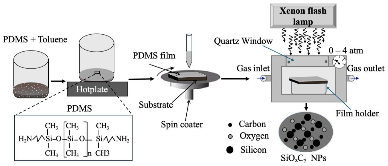
Figure 2.
Experimental flowchart summarizing the synthesis route and characterization.
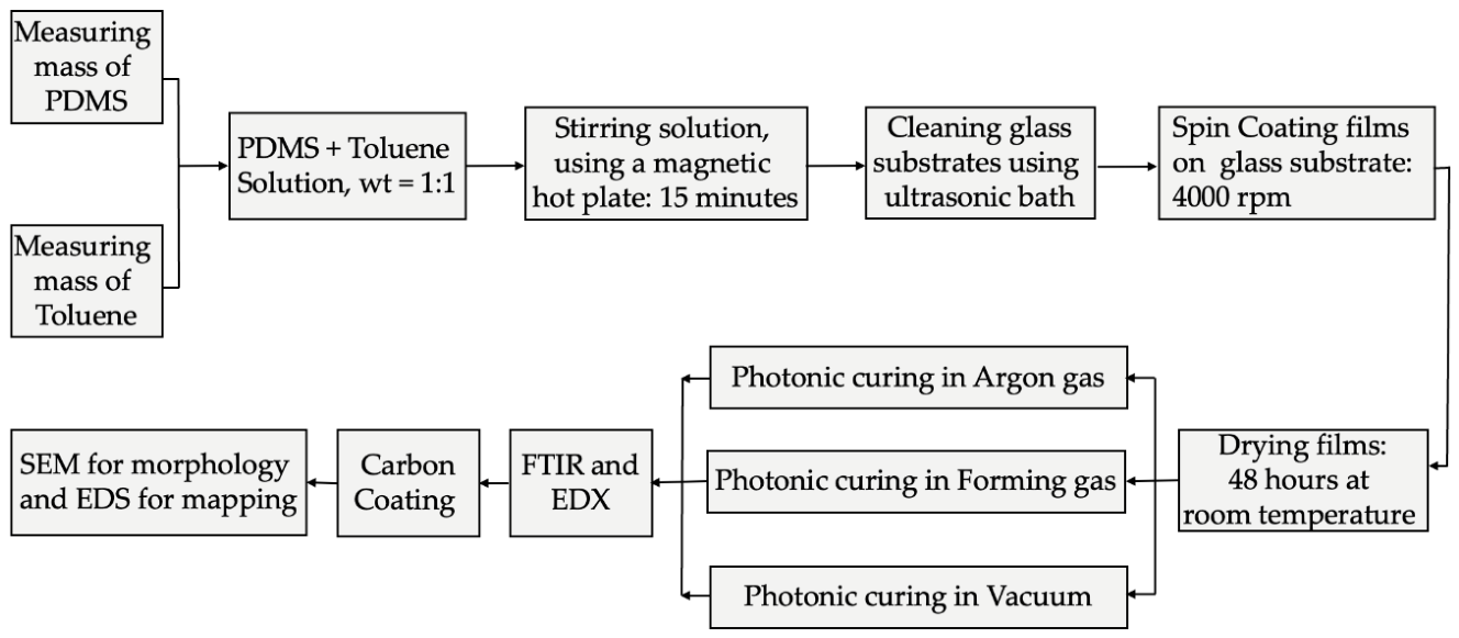
Figure 3.
Comparison of FTIR results of an uncured and photonically cured PDMS processed under vacuum, argon, and forming gas environments at different values of photonic curing parameters. (a) Spectra obtained after curing at 2 atm and 2.04 J/cm2. (b) Spectra obtained at 2 atm and 4.08 J/cm2. (c) Spectra obtained at 3 atm and 4.08 J/cm2, showing the strongest structural transformation under forming gas. (d) Spectra obtained at 4 atm and 4.08 J/cm2, illustrating that increasing pressure beyond 3 atm does not further enhance PDMS decomposition.
Figure 3.
Comparison of FTIR results of an uncured and photonically cured PDMS processed under vacuum, argon, and forming gas environments at different values of photonic curing parameters. (a) Spectra obtained after curing at 2 atm and 2.04 J/cm2. (b) Spectra obtained at 2 atm and 4.08 J/cm2. (c) Spectra obtained at 3 atm and 4.08 J/cm2, showing the strongest structural transformation under forming gas. (d) Spectra obtained at 4 atm and 4.08 J/cm2, illustrating that increasing pressure beyond 3 atm does not further enhance PDMS decomposition.
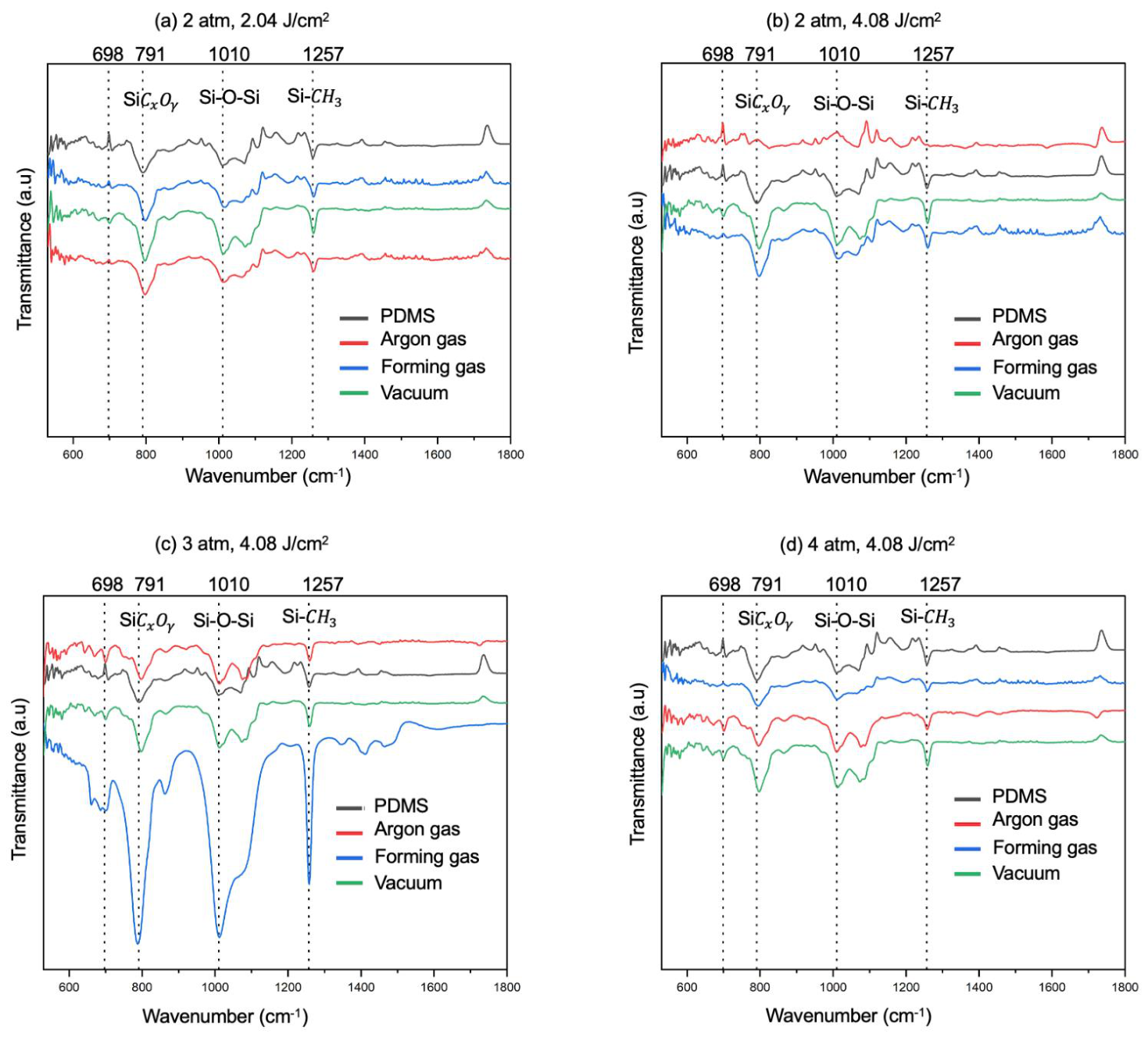
Figure 7.
Illustration of the degradation pathways and reaction environments that shaped the PDMS restructuring and Si nanostructure formation under different photonic curing conditions.
Figure 7.
Illustration of the degradation pathways and reaction environments that shaped the PDMS restructuring and Si nanostructure formation under different photonic curing conditions.
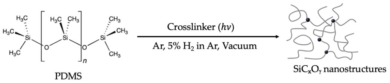

Table 1.
Photonic curing parameters.
| Pressure (atm) | Time (µs) | Duty cycle (%) | Rate (Hz) | Counts | Voltage (Volts) | Fluence (J/cm2) |
|
0 – 4 |
1000 |
50 |
1.0 |
4 |
450 | 2.04 |
| 500 | 2.64 | |||||
| 600 | 4.08 |
Disclaimer/Publisher’s Note: The statements, opinions and data contained in all publications are solely those of the individual author(s) and contributor(s) and not of MDPI and/or the editor(s). MDPI and/or the editor(s) disclaim responsibility for any injury to people or property resulting from any ideas, methods, instructions or products referred to in the content. |
© 2026 by the authors. Licensee MDPI, Basel, Switzerland. This article is an open access article distributed under the terms and conditions of the Creative Commons Attribution (CC BY) license (http://creativecommons.org/licenses/by/4.0/).
Copyright: This open access article is published under a Creative Commons CC BY 4.0 license, which permit the free download, distribution, and reuse, provided that the author and preprint are cited in any reuse.