
Submitted:
21 September 2026
Posted:
22 September 2026
You are already at the latest version
Abstract
Cadmium telluride (CdTe) is a direct-bandgap semiconductor with strong optical absorption and is therefore well suited to thin-film photovoltaic conversion. This study brings together the AFORS-HET modeling work on CdS/CdTe devices, the figures and material-parameter table, and supporting literature supplied with the project. The analysis focuses on three closely connected limitations: formation of a non-ohmic Schottky barrier at the metal back contact, use of a highly doped electron-reflector (ER) region to modify carrier transport near that contact, and surface recombination velocity as an effective model for pinhole- or defect-related losses. The simulations indicate that back-contact and interface conditions influence open-circuit voltage much more strongly than short-circuit current density. Optimized modeled structure using an ER, a doping concentration of 7 × 1018 cm-3, an ER thickness of 100 nm, and an effective barrier height of approximately 0.1 eV reaches a simulated efficiency of 19.83%, with Voc = 917.6 mV and Jsc = 28.45 mA/cm². The surface-recombination study further shows that severe pinhole conditions can lower Voc to approximately 0.73 V. These results are interpreted together with literature on CdTe doping, interface engineering, minority-carrier lifetime, grain-boundary recombination, and Cu-related back-contact effects [1-7]. The combined picture emphasizes that high optical absorption alone is not sufficient: contact selectivity, interface quality, carrier lifetime, and defect control must be optimized simultaneously.
Keywords:
back-contact schottky barriers
; electron-reflector layers
; surface recombination
; and pinhole-related losses
1. Introduction
Photovoltaic devices convert incident solar radiation directly into electrical energy. CdTe is particularly attractive for thin-film photovoltaics because its direct bandgap and high absorption coefficient permit strong absorption in a semiconductor layer only a few micrometers thick. The study uses a 2 µm CdTe absorber as a representative manufacturing-scale thickness and combines it with a thin CdS window layer and a ZnO transparent conducting oxide (TCO) [8,9,10,11]. The paper also cites earlier CdTe fabrication work and a ZnO/CdS/CdTe performance review in support of this device context [12,13].
The central difficulty addressed here is not simply generation of photocarriers, but extraction of those carriers without losing the voltage that the absorber is capable of producing. The modeling identifies the CdTe back contact as a major electrical bottleneck. Because the work function of commonly used metals may be insufficient to form an ideal ohmic contact to p-type CdTe under the assumed material parameters, a Schottky-type barrier can develop. That barrier changes the band profile near the rear of the device and can enhance recombination or impede majority-carrier transport, reducing Voc and efficiency [10,11,14]. The back-contact/ER modeling is also grounded in the project publications on the Schottky-barrier electron-reflector concept and CdS/CdTe device modeling [15,16].
The supporting literature supplied with this project broadens this picture. High acceptor concentrations have been pursued through in-situ arsenic doping, and carrier-concentration limitations in polycrystalline CdTe have been directly investigated [8,9]. Other work emphasizes interface engineering as a route toward higher CdTe efficiency [17], impurity-distribution control for improved minority-carrier lifetime [18], recombination associated with different grain-boundary types [19], and changes in lifetime and hole concentration caused by Cu-containing back-contact treatments [20,21]. These studies support treating doping, lifetime, recombination, and contact design as coupled rather than independent variables. Recent work further updates this materials picture: a 2024 review summarizes current CdTe doping engineering with Group I and Group V dopants, while 2025 experiments using AsCl3 vapor annealing in polycrystalline CdSeTe report enhanced dopant activation, carrier lifetime above 72 ns, and approximately 18% device efficiency [22,23].
AFORS-HET is used as the primary device-simulation framework [24]. Its value in this study is the ability to vary material, transport, interface, optical, and contact parameters systematically. This allows the model to distinguish changes that primarily affect current generation and collection from changes that primarily affect voltage. Simulation is therefore used as a guide for experimental optimization rather than as a substitute for fabrication and measurement.
2. Relationship to Previously Reported Back-Contact and Electron-Reflector Work
The present investigation builds directly upon the back-contact Schottky-barrier and electron-reflector (ER) modeling acknowledged in Ref. 3 of the original paper and the prior conference work is listed as Ref. [15]. This attribution is important because the ER/back-contact optimization was not developed for the first time in the present pinhole study; rather, it provides the established device framework on which the surface-recombination analysis is built [15].
In the previously reported work, the rear metal/p-CdTe contact was treated as a potentially non-ohmic contact whose Schottky barrier can limit the voltage obtainable from a CdS/CdTe thin-film solar cell. The simulations showed that changing the rear-contact energetics has a much stronger influence on the high-voltage portion of the illuminated J-V characteristic and on open-circuit voltage than on short-circuit current density. This distinction provides the physical motivation for concentrating on rear-contact engineering even when the absorber continues to generate nearly the same photocurrent [15].
A central element of that earlier approach was the introduction of a highly doped ER region adjacent to the CdTe back contact. The ER modifies the rear energy-band profile and narrows the depletion region associated with the back-contact barrier. In the intended transport picture, the thin and heavily doped rear region promotes majority-hole extraction, including transport through a sufficiently narrow barrier, while reducing the access of minority electrons to a recombination-active metal interface. The broader electron-reflector strategy is also discussed in Hsiao's CdTe thin-film solar-cell work [10], and the importance of rear-contact design for CdTe voltage is consistent with the voltage-improvement strategies discussed by Sites and Pan [11].
The earlier modeling established the basis for varying ER thickness, ER doping concentration, and effective back-contact barrier height. The reported optimized condition - approximately 100 nm ER thickness, 7 × 1018 cm-3, ER doping, and an effective barrier height near 0.1 eV - is therefore treated in this report as a previously established back-contact/ER design point rather than as a new result of the pinhole analysis [15]. The corresponding simulated performance, including Voc = 917.6 mV, Jsc = 28.45 mA/cm2, and efficiency = 19.83%, is retained because it defines the optimized baseline from which the surface-recombination sensitivity is evaluated.
The principal extension in the present work is the use of rear-region surface recombination velocity as an effective pinhole or severe-interface-defect parameter. Starting from the previously optimized ER/back-contact framework, the model varies this recombination parameter to determine how departures from an ideal rear interface alter the illuminated J-V response. The resulting comparison separates two related but distinct questions: the earlier work asks how favorable rear-contact energetics and ER design can recover voltage, whereas the present extension asks how strongly that optimized voltage is degraded when recombination-active defects are introduced near the same interface.
Viewed sequentially, the two studies lead to a more complete physical interpretation. Back-contact band engineering is necessary to reduce the nominal Schottky-barrier limitation, but favorable band alignment alone is not sufficient if the rear region contains strong recombination pathways. The ER design controls carrier selectivity and transport, while the surface-recombination model represents the quality of the interface through which those carriers must be extracted. Consequently, the present study should be understood as an extension and sensitivity analysis of the acknowledged Ref. [3] back-contact work, not as a replacement or independent re-derivation of that earlier contribution [15].
2.1. Device Architecture and Energy-Band Design
The baseline architecture is TCO/CdS/CdTe/ER/metal. The ZnO TCO is modeled as an n-type, wide-bandgap front contact; CdS is the n-type window layer; CdTe is the p-type absorber; and the ER region is placed near the rear contact. In the structure, the ZnO thickness is 500 nm, the CdS thickness is 40 nm, and the CdTe absorber thickness is 2 µm. The CdTe absorber doping is 7 × 1016 cm-3, while CdS and ZnO are modeled near 7 × 1018 cm-3. The CdTe and ER carrier lifetime is taken as 1 × 10⁻⁹ s in the reported simulation. Related numerical studies of CdS/CdTe and CdS/CdTe/ZnTe structures provide additional context for thickness-dependent device behavior [25], while CdS-related voltage and fill-factor effects have also been examined experimentally and analytically [26]. Recent CdS studies also show that deposition temperature and fluorine doping can modify CdS structural, optical, and electrical properties and measurably affect CdS/CdTe device performance [27].
Figure 1 makes the purpose of the ER region clearer than a layer sequence alone. The principal junction is established at the CdS/CdTe interface, while the rear ER region modifies the band profile close to the back contact. The figure reports a CdS/CdTe conduction-band offset of approximately 0.22 eV and a valence-band offset of approximately 0.89 eV. The wide-bandgap TCO and CdS layers are intended to transmit useful radiation to the CdTe absorber while providing appropriate electrical selectivity.
A useful interpretation of the architecture is that the front junction and the back contact perform different carrier-selection functions. The CdS/CdTe heterojunction separates photogenerated carriers, while the rear structure must extract holes without becoming an efficient sink for minority electrons. The ER concept is introduced specifically to improve this rear selectivity and to reduce the adverse electrical influence of the metal/CdTe barrier. Recent front-interface work also shows that interface passivation remains a major lever in modern CdTe-family devices: a SnO2/ZnO n-type bilayer in As-doped CdSeTe/CdTe was reported to reduce interface recombination and support 21.7% efficiency, illustrating how carrier-selective interfaces complement the rear-contact strategy considered here [28].
2.2. Material Parameters Used in the Simulation
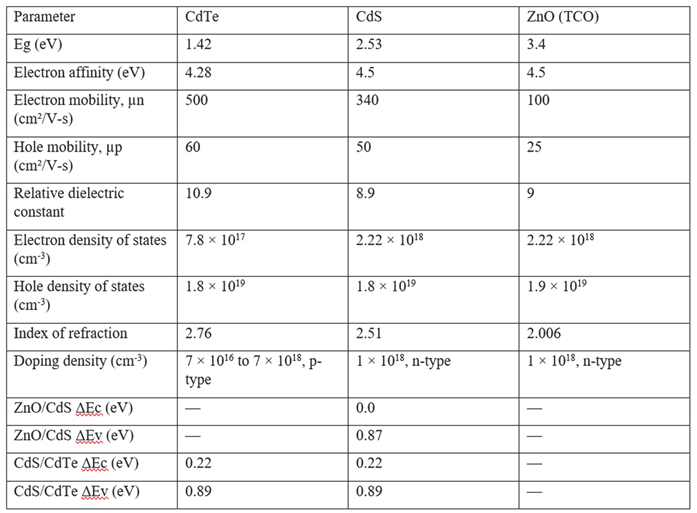
Table 1 reproduces the material parameters reported in this study. These parameters define the electronic structure and transport assumptions used by the AFORS-HET model. They should therefore be regarded as model inputs rather than universal constants; differences in deposition method, microstructure, composition, activation, and defect density can cause experimental values to vary.
The doping range in Table 1 is especially important because the absorber and the highly doped ER region play different roles. The absorber must support a useful depletion and collection region, whereas the ER is intentionally driven to a much higher p-type carrier concentration in the optimized case. The supplied literature on arsenic and in-situ doping [8,9] is therefore directly relevant to the practical question of whether high acceptor concentrations can be achieved and maintained in polycrystalline CdTe-related layers.
2.3. Back-Contact Schottky Barrier
For p-type CdTe, the metal work function and semiconductor electron affinity/bandgap determine the contact energetics. The report gives a CdTe electron affinity of 4.28 eV and discusses the difficulty of obtaining an ideal ohmic contact with common metals. Cu, Ni, and Ti are cited as examples of metals whose work functions can lead to non-ohmic behavior under the model assumptions. Although the numerical work-function threshold is presented somewhat differently in separate portions of the original text, the physical conclusion is consistent: a rear barrier can form and can limit voltage. Back-contact buffer approaches using MoOx and MoO3-x/Au have likewise been investigated as alternative strategies for improving rear-contact behavior [5,6]. The continuing importance of the rear-contact barrier is demonstrated by recent experimental contact studies. Solution-processed CuBr has been reported to reduce the back-contact barrier while simultaneously providing Cu doping, increasing Voc and eliminating characteristic rollover behavior [29]. An optimized NiTe2/Ni back contact formed by chemical processing and sputtering has likewise produced CdTe devices above 18% efficiency with Voc above 800 mV and fill factor above 70% [30].
Figure 2 illustrates why the back-contact problem appears most strongly in Voc. At short circuit, the internal field and external circuit favor extraction, so the simulated photocurrent remains close to its maximum value. Near open circuit, however, the net terminal current approaches zero and the carrier populations build up. Recombination and unfavorable contact energetics then have a larger effect on the attainable quasi-Fermi-level separation and therefore on Voc. This explains why a device can preserve nearly the same Jsc while losing a substantial amount of voltage.
This behavior also means that Jsc alone is an incomplete diagnostic for rear-contact quality. A device may appear optically and photogeneratively healthy while still suffering a serious contact-induced efficiency loss. For experimental validation, the full J-V curve, Voc, fill factor, and preferably spectral response should therefore be evaluated together.
2.4. Electron-Reflector Extended Region
Building on the back-contact/ER framework acknowledged as Ref. 3 in the original paper [15], the ER region is introduced near the back contact to mitigate the Schottky-barrier problem. In the model it is a thin, heavily doped p-type region that modifies the rear band profile. The intended effect is twofold: the narrow, highly doped region can facilitate majority-hole transport through a thin barrier, while the expanded-bandgap or reflector-like profile can reduce minority-electron access to the recombination-active rear contact. Candidate CdTe-related wider-bandgap materials mentioned in the source material include CdZnTe, CdMnTe, and CdMgTe. The electron-reflector concept is treated directly in Hsiao’s dissertation on CdTe thin-film solar cells [10], and voltage-improvement strategies for CdTe devices are discussed by Sites and Pan [11]. The ER-thickness and doping trends discussed below should therefore be read as part of that previously established optimization framework [15]. Recent back-buffer and passivation studies provide experimental analogues to the carrier-selective function sought with the ER concept. A CuxByO back-buffer layer has been reported to increase carrier concentration and lifetime in ultra-thin CdTe devices [31], while a Cu-In-O back-interface layer produced simultaneous chemical and field passivation, suppressed rear recombination, increased carrier lifetime, and raised Voc from 723 to 798 mV [32]. These results support the broader principle that rear-band engineering and interface passivation must be optimized together.
The trend in Figure 3 shows that changing the ER region can improve voltage, but thickness cannot be optimized from Voc alone. A thicker ER region also becomes an additional optical and transport layer. Consequently, the original work argues for a thin, highly doped region rather than simply maximizing ER thickness. The optimum reported later in the study uses a 100 nm ER layer with a doping concentration of 7 × 1018 cm-3. The distinction between thickness and doping is important. Thickness changes the physical distance over which the rear band profile and absorption act, whereas doping changes depletion width, electric field, and tunneling probability. These parameters therefore need to be optimized together. The model result should be understood as identifying a favorable parameter combination under the stated assumptions rather than a universal optimum for all CdTe fabrication routes.
2.5. Electrical Characteristics and Recombination
The analysis identifies an extended portion of the current-voltage characteristic below approximately 0.8 V that can be represented by an ideality factor of about n = 2. Within the interpretation used in the source, this behavior indicates that recombination in the space-charge region is an important current mechanism. The simulated maximum short-circuit current density is approximately 28.4 mA/cm² and is used as a relatively stable reference throughout the parameter study. Grain-boundary and defect-related recombination remain important complementary mechanisms in polycrystalline CdTe [19,33].
The n ≈ 2 observation is consistent with the broader emphasis of the project: voltage and fill-factor losses cannot be understood solely from optical absorption. Recombination pathways inside the depletion region, at grain boundaries, and at interfaces can all influence the illuminated diode response. The supporting grain-boundary study [19] reinforces the relevance of microstructure-dependent recombination in polycrystalline CdTe, while the impurity-distribution study [18] emphasizes the connection between material processing and minority-carrier lifetime.
More recent CdTe-family work continues to emphasize the coupling among doping, lifetime, and interface quality. The 2024 doping review summarizes the tradeoffs of Cu and Group-V strategies [22], and AsCl3 vapor diffusion doping of CdSeTe demonstrates that high carrier lifetime and useful Voc can be obtained when dopant incorporation and activation are controlled [23].
The added literature helps place the simulation variables in a broader experimental context. Kartopu et al. report polycrystalline CdTe cells with high acceptor concentrations achieved by in-situ arsenic doping [8], while McCandless et al. address carrier-concentration limits through in-situ doping [9]. These references support the experimental relevance of treating acceptor concentration as a major design variable rather than as a fixed material property. Processing-dependent changes in CdTe, including CdCl2 treatment, are also relevant because they can alter physical properties that ultimately affect junction and recombination behavior [2].
Figure 4.
Semilogarithmic simulated current-density characteristics. The extended region below approximately 0.8 V is described by an ideality factor near n = 2, consistent in the model with strong space-charge-region recombination.
Figure 4.
Semilogarithmic simulated current-density characteristics. The extended region below approximately 0.8 V is described by an ideality factor near n = 2, consistent in the model with strong space-charge-region recombination.
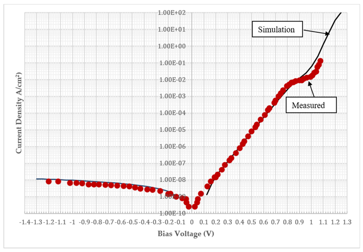
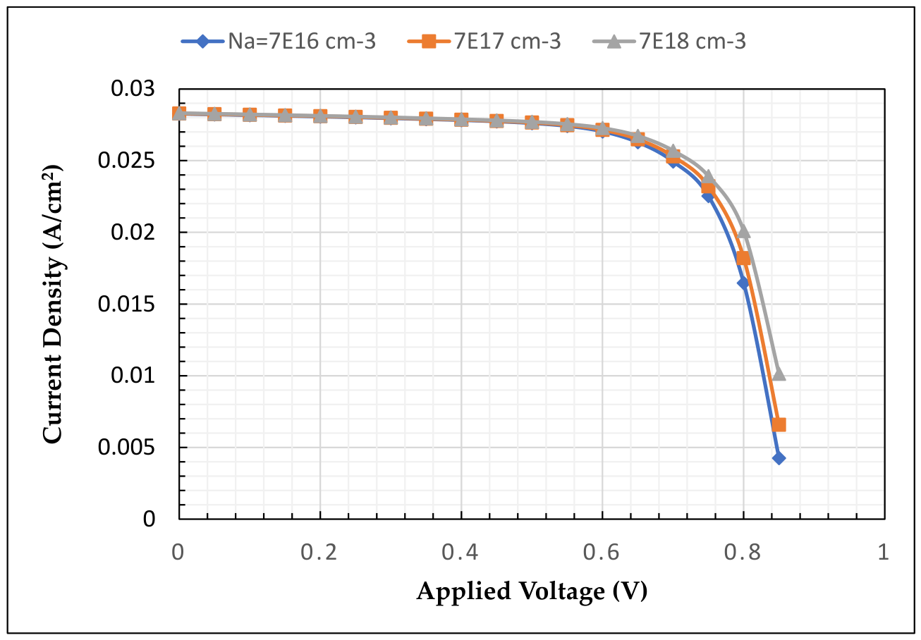
Figure 5.
Simulated J-V curves for different ER doping densities. Increasing ER doping shifts the rear-contact-limited portion of the curve and supports a higher-voltage operating condition in the model.
Figure 5.
Simulated J-V curves for different ER doping densities. Increasing ER doping shifts the rear-contact-limited portion of the curve and supports a higher-voltage operating condition in the model.
Carrier concentration alone is not sufficient, because increased doping must be considered together with minority-carrier lifetime and recombination. Kranz et al. investigate impurity-distribution tailoring for enhanced minority-carrier lifetime [18]. Moseley et al. examine recombination by grain-boundary type [19]. Taken together, these works reinforce a key modeling lesson: a nominally favorable doping level may not translate into higher device voltage if the associated defects, impurities, or interfaces increase recombination. Structural and optical properties of the CdS window layer can likewise depend on deposition chemistry [1], so absorber optimization should be considered together with front-layer quality.
The rear contact adds another layer of coupling. Gessert et al. report dependence of carrier lifetime on Cu-contacting temperature and ZnTe:Cu thickness [20], while Korevaar et al. map hole concentrations as a function of copper treatment [21]. These studies are directly relevant to a CdTe back-contact model because Cu can influence both electrical activation and recombination. Thus, back-contact optimization is not merely a choice of metal work function; in real devices it is also a processing and defect-control problem. Rear-contact studies using MoOx or MoO3-x/Au buffers provide further examples of contact engineering intended to reduce losses at the CdTe back interface [5,6].
Ablekim, Colegrove, and Metzger frame interface engineering as a route toward 25% CdTe solar cells [17]. That perspective is consistent with the simulation: the largest gains are expected when the absorber, junction, rear contact, and recombination-active interfaces are treated as an integrated system. The ER concept addresses rear selectivity, while doping and lifetime engineering address the bulk and microstructural conditions needed to preserve the resulting voltage.
The ER doping sweep shows why a heavily doped rear region is central to the proposed contact design. The reported optimized concentration is 7 × 1018 cm-3, substantially higher than the 7 × 1016 cm-3, baseline absorber concentration. Such a concentration difference creates a p/p+ type rear structure and narrows the region associated with the rear barrier. The practical feasibility of high acceptor concentration is therefore an important experimental question, making the supplied in-situ doping studies [8,9] particularly relevant.
The optimized ER/back-contact design point used here originates from the previously acknowledged modeling work [15]. The optimized simulation combines an ER thickness of 100 nm, an ER doping concentration of 7 × 1018 cm-3, and an effective barrier height of approximately 0.1 eV. Under these assumptions the model reaches 19.83% efficiency, Voc = 917.6 mV, and Jsc = 28.45 mA/cm². Figure 6 is particularly useful because it shows both the J-V response and the power-density curve; the power maximum occurs below Voc, as expected, and represents the operating point used in the simulated efficiency calculation. In the present study, this optimized condition serves as the baseline for evaluating the additional effect of surface-recombination/pinhole losses.
The optimized result is best interpreted as a design target. It demonstrates what the modeled architecture can produce when the contact barrier, ER properties, and recombination assumptions are simultaneously favorable. It does not establish that a fabricated cell will automatically reach the same performance. Experimental deviations in carrier concentration, lifetime, interface state density, band alignment, series resistance, shunting, grain structure, and contact chemistry can all move the measured device away from the simulated condition.
2.6. Surface Recombination Velocity as A Pinhole Model
The physical importance of this parameter is reinforced by a recent CdTe study that extracts back-surface recombination velocity and back-interface band bending from backside quantum-efficiency measurements and uses them to determine interface and bulk recombination currents at open circuit [34]. Patterned Al2O3 back-contact experiments on CdS/CdTe cells also directly connect microhole/contact geometry with passivation and carrier-transport losses, providing an experimental context for interpreting pinhole-related rear-interface effects [35]. The surface-recombination analysis is the principal extension beyond the previously acknowledged ER/back-contact optimization [15]. The work uses surface recombination velocity at the rear region as an effective model for pinholes or severe local interface defects. This is a simplified representation: it does not explicitly reproduce the geometry of every pinhole. Instead, it asks how strongly the electrical response changes when carriers reaching the rear interface are allowed to recombine at different rates. This makes surface recombination velocity a useful sensitivity parameter for assessing defect severity within a one-dimensional device model.
Figure 7.
Summary of simulated J-V curves for surface recombination velocities from 104 to 107 cm/s. In the reported model, Jsc remains comparatively stable while the voltage at which the curves approach zero current shifts substantially.
Figure 7.
Summary of simulated J-V curves for surface recombination velocities from 104 to 107 cm/s. In the reported model, Jsc remains comparatively stable while the voltage at which the curves approach zero current shifts substantially.
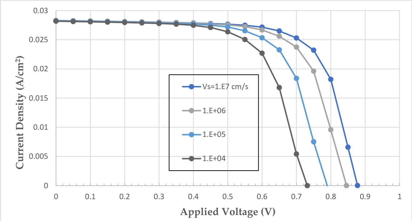
The principal reported consequence is a change in Voc rather than a large change in Jsc. The optimized case is associated with a surface recombination velocity of approximately 1 × 107 cm/s and retains Voc = 917.6 mV and Jsc = 28.45 mA/cm². The severe-pinhole case represented by 10,000 cm/s reduces Voc to approximately 0.73 V. The direction assigned to “ideal” and “severe” surface velocity in the model is retained here exactly as reported, even though surface-recombination-velocity conventions can differ among modeling setups; this point should be checked carefully when reproducing the AFORS-HET boundary conditions. Broader reviews of CdS/CdTe achievements and challenges [36] and work on manufacturable window layers and CdTe thickness [3] reinforce the need to optimize the complete device stack rather than a single layer in isolation. The important device-level observation is robust within the source study: the pinhole/interface parameter primarily changes the voltage-producing capability of the cell. A defect can therefore cause a large efficiency penalty without proportionally suppressing the photogenerated current. This again makes Voc a sensitive indicator of rear-interface quality.
3. Results and Discussions
The figures and parameter sweeps point to a common mechanism. The CdTe absorber can generate a large photocurrent because of its favorable optical properties, but the conversion of that photogeneration into high terminal voltage depends on the electrical boundary conditions. A rear Schottky barrier, recombination-active interface, or defective region can lower the carrier population separation that produces Voc even when the absorber continues to generate nearly the same short-circuit current. Earlier high-efficiency CdS/CdTe device work [37], numerical thickness studies [25], and cross-sectional electric-field measurements [14] provide useful experimental and modeling context for interpreting these coupled effects.
This explains the repeated pattern in the simulations: Jsc is comparatively insensitive to moderate changes in rear-contact barrier height, ER thickness, and the modeled surface-recombination condition, while Voc moves substantially. The ER layer improves the rear band profile and carrier selectivity; high p-type ER doping narrows the rear barrier region; and interface-quality control limits recombination. These mechanisms are complementary rather than competing explanations.
The model also suggests an experimental diagnostic sequence. If Jsc is near the expected value but Voc is low, attention should first turn to recombination and contact selectivity rather than to absorber optical thickness alone. If both Jsc and Voc are low, optical absorption, junction collection, bulk lifetime, shunting, and contact effects may all need to be considered. Comparing measured J-V curves with the simulated trends can therefore help identify which physical parameter family is most likely responsible for a performance deficit. Recent studies sharpen this interpretation by showing that recombination velocity can be measured or inferred at specific interfaces [28,34], and that modern rear-buffer/contact layers can improve voltage through a combination of barrier reduction, field formation, chemical passivation, and carrier-density control [29,30,31,32].
3.1. Recommended Optimization and Validation Sequence
- o Establish the front stack. Use the 500 nm ZnO TCO and 40 nm CdS window as the baseline reported in the model, then verify optical transmission and junction behavior before modifying the rear structure.
- o Establish the CdTe absorber baseline. Begin near the modeled 2 µm thickness and 7 × 1016 cm-3 p-type concentration. Measure or estimate carrier lifetime because doping and lifetime must be interpreted together [8,9,18]. Recent CdTe doping literature provides additional experimental benchmarks for this step, particularly for Group-V activation and carrier-lifetime improvement [22,23].
- o Characterize the rear-contact limitation. Use Voc, fill factor, and the full J-V shape to determine whether the device exhibits behavior consistent with a significant rear barrier. Do not rely on Jsc alone.
- o Introduce and optimize the ER region. Treat thickness and doping as coupled parameters. The reported high-performance point is 100 nm and 7 × 1016 cm-3, but experimental optimization should verify whether the same balance applies to the fabricated material.
- o Evaluate interface and pinhole sensitivity. Compare devices or simulations across a controlled range of rear-interface conditions and use Voc degradation as a sensitive indicator of recombination-related loss. Where possible, complement J-V analysis with interface-sensitive measurements capable of constraining recombination velocity or band bending, as demonstrated in recent CdTe studies [28,34].
- o Examine Cu and contact-processing effects. Because Cu treatment can modify both hole concentration and carrier lifetime [20,21], contact recipes should be correlated with electrical measurements rather than evaluated only by nominal composition. Recent CuBr back-contact results also illustrate that contact-barrier reduction and Cu doping can occur simultaneously and therefore should be separated experimentally when interpreting performance changes [29].
- o Close the simulation-experiment loop. Compare measured J-V and spectral-response data with AFORS-HET results, update uncertain parameters, and repeat. The purpose of the model is to reduce the experimental search space and identify physically meaningful targets.
3.2. Limitations and Points Requiring Experimental Verification
Several aspects of this study should remain explicitly identified as modeling assumptions. First, the 19.83% efficiency is simulated and depends on the selected lifetimes, mobilities, densities of states, absorption inputs, interface parameters, and contact boundary conditions. Second, the surface-recombination-velocity treatment is an effective pinhole model rather than a geometrically resolved representation of a physical pinhole. Third, the original source contains small internal differences in the stated CdTe bandgap and the work function required for an ohmic contact; the discussion therefore preserves the reported parameter table and emphasizes the qualitative contact conclusion rather than silently forcing those statements into a single value.
A further limitation is dimensionality. The discussion proposes more accurate two-dimensional modeling in connection with experimental work. This is especially relevant to pinholes, grain boundaries, and local shunts because those defects are spatially nonuniform. A one-dimensional surface-velocity model can quantify sensitivity but cannot reproduce all lateral current paths. Experimental microscopy, local electrical characterization, and two-dimensional simulation would therefore be valuable extensions. Random-deposition modeling of CdS layers [7] illustrates why spatial nonuniformity can matter, while the AFORS-HET numerical framework and characterization methods are described further by Stangl, Haschke, and Leendertz [38]. Recent patterned-back-contact work is especially relevant here because micrometer-scale contact openings produce intrinsically two-dimensional current-flow and passivation problems that cannot be represented fully by a single one-dimensional surface-velocity parameter [35].
4. Conclusions
The results support a coherent design strategy for CdS/CdTe thin-film solar cells. CdTe provides the optical foundation, but the attainable voltage and efficiency are strongly controlled by electrical losses at the rear contact and interfaces. The simulated back-contact Schottky barrier primarily reduces Voc, while Jsc remains comparatively stable. A thin, heavily doped ER region can improve rear-contact behavior by modifying the band profile and carrier transport.
The reported optimized structure uses a 100 nm ER layer, an ER doping concentration of 7 × 1018 cm-3, and an effective barrier height of approximately 0.1 eV. It produces a simulated efficiency of 19.83%, Voc = 917.6 mV, and Jsc = 28.45 mA/cm². Surface-recombination modeling further shows that the modeled severe-pinhole condition can reduce Voc to about 0.73 V. The literature supplied with the project reinforces the importance of high and controllable acceptor concentration, minority-carrier lifetime, grain-boundary recombination, interface engineering, and Cu-related contact processing [1,2,3,4,5,6,7].
The broader implication is that future optimization should not treat the absorber, rear contact, ER region, and defects independently. The highest-value experimental program is one that measures doping, lifetime, contact behavior, and interface quality together and uses those measurements to refine the simulation. In that role, AFORS-HET provides a practical framework for converting observed performance losses into testable hypotheses about the underlying device physics. At the module and application level, improvements in device efficiency and specific power can also affect the range of viable photovoltaic markets [39]. The recent literature confirms that these issues remain active design priorities: advances in CdS window properties [27], Group-V doping [22,23], quantitative interface-recombination analysis [28,34], and low-barrier/passivating rear contacts [29,30,31,32] all point toward coordinated control of transport, recombination, and contact energetics.
References
- Zhao, X. H.; et al. Structural and optical properties of CdS thin films prepared by chemical bath deposition at different ammonia concentration and S/Cd molar ratios. J. Mater. Sci. Mater. Electron. 2013, vol. 24, 457–464. [Google Scholar] [CrossRef]
- Razykov, T. M.; et al. Effect of CdCl2 treatment on physical properties of CdTe films with different compositions fabricated by chemical molecular beam deposition. Appl. Sol. Energy 2013, vol. 49, 35–40. [Google Scholar] [CrossRef]
- Korevaar, B. A.; et al. High efficiency CdTe cells using manufacturable window layers and CdTe thickness. Thin Solid Films, 2013. [Google Scholar]
- Hou, T.-C.; et al. Nanogenerator based on zinc blende CdTe micro/nanowires. Nano Energy 2013, vol. 2, 387–393. [Google Scholar] [CrossRef]
- Lin, H.; Xia, W.; Wu, H. N.; Tang, C. W. CdS/CdTe solar cells with MoOx as back-contact buffers. Appl. Phys. Lett. 2010, vol. 97(no. 12), Art. no. 123504. [Google Scholar] [CrossRef]
- Paudel, N. R.; et al. Sputtered CdS/CdTe solar cells with MoO3-x/Au back contacts. Sol. Energy Mater. Sol. Cells 2013, vol. 113, 26–31. [Google Scholar] [CrossRef]
- Chen, L. Random Deposition Model of CdS Layers in CdS/CdTe Thin-Film Solar Cells. Master’s thesis, Colorado State Univ., Fort Collins, CO, USA, 2008. [Google Scholar]
- Kartopu, G.; et al. Study of thin film poly-crystalline CdTe solar cells presenting high acceptor concentrations achieved by in-situ arsenic doping. Sol. Energy Mater. Sol. Cells 2019, vol. 194, 259–267. [Google Scholar] [CrossRef]
- McCandless, B. E.; et al. Overcoming carrier concentration limits in polycrystalline CdTe thin films with in-situ doping. Sci. Rep. 2018, vol. 8, Art. no. 14519. [Google Scholar] [CrossRef]
- Hsiao, K. Electron-Reflector Strategy for CdTe Thin-Film Solar Cells. Ph.D. dissertation, Colorado State Univ., Fort Collins, CO, USA, 2010. [Google Scholar]
- Sites, J.; Pan, J. Strategies to increase CdTe solar-cell voltage. Thin Solid Films 2007, vol. 515, 6099–6102. [Google Scholar] [CrossRef]
- Morris, G. C.; Das, S. K. Some fabrication procedures for electrodeposited CdTe solar cells. Int. J. Sol. Energy 1992, vol. 12(no. 1–4), 95–108. [Google Scholar] [CrossRef]
- Putra, N. M. D.; Sugianto; Marwoto, P.; Murtafiatin, R.; Rizaldi, P. D. Performance profile analysis of ZnO/CdS/CdTe solar cells thin film: A review of absorber thickness and device temperature. J. Phys. Conf. Ser. 2019, vol. 1567. [Google Scholar]
- Moutinho, H. R.; et al. Investigation of potential and electric field profiles in cross sections of CdTe/CdS solar cells using scanning Kelvin probe microscopy. J. Appl. Phys. 2010, vol. 108, Art. no. 074503. [Google Scholar] [CrossRef]
- Rampalli, C. S.; Fardi, H. 50th IEEE Photovoltaic Specialists Conference (PVSC), San Juan, Puerto Rico. 2023. [Google Scholar] [CrossRef]
- Fardi, H.; Buny, F. Characterization and Modeling of CdS/CdTe Heterojunction Thin-Film Solar Cell for High Efficiency Performance. International Journal of Photoenergy. Article ID 576952. 2013. [Google Scholar]
- Ablekim, T.; Colegrove, E.; Metzger, W. K. Interface engineering for 25% CdTe solar cells. ACS Appl. Energy Mater. 2018, vol. 1, 5135–5139. [Google Scholar] [CrossRef]
- Kranz, L.; et al. Tailoring impurity distribution in polycrystalline CdTe solar cells for enhanced minority carrier lifetime. Adv. Energy Mater. 2014, vol. 4, Art. no. 1301400. [Google Scholar] [CrossRef]
- Moseley, J.; et al. Recombination by grain-boundary type in CdTe. J. Appl. Phys. 2015, vol. 118, Art. no. 025702. [Google Scholar] [CrossRef]
- Gessert, T. A.; et al. Dependence of carrier lifetime on Cu-contacting temperature and ZnTe:Cu thickness in CdS/CdTe thin-film solar cells. Thin Solid Films 2009, vol. 517, 2370–2373. [Google Scholar] [CrossRef]
- Korevaar, B. A.; Zorn, G.; Raghavan, K. C.; Cournoyer, J. R.; Dovidenko, K. Cross-sectional mapping of hole concentrations as a function of copper treatment in CdTe photovoltaic devices. Prog. Photovolt. 2015, vol. 23, 1466–1474. [Google Scholar] [CrossRef]
- Duan, X.-M.; Wang, Y.-Z.; Yan, F. Doping engineering in the CdTe thin film solar cells. cMat 2024, vol. 1(no. 3), e29. [Google Scholar] [CrossRef]
- Duan, X.; et al. Doping in Efficient Polycrystalline CdSeTe Solar Cells via AsCl3 Vapor Annealing. ACS Appl. Energy Mater. 2025, vol. 8(no. 7), 4265–4271. [Google Scholar] [CrossRef]
- Froitzheim; Stangl, R.; Elstner, L.; Kriege, W.; Fuhs, W. AFORS-HET: A Computer Program for the Simulation of Heterojunction Solar Cells to Be Distributed for Public Use. Master’s thesis, Hahn-Meitner-Institut, Berlin, Germany, 2009. [Google Scholar]
- Amin, N.; Sopian, K.; Konagai, M. Numerical modeling of CdS/CdTe and CdS/CdTe/ZnTe solar cells as a function of CdTe thickness. Sol. Energy Mater. Sol. Cells 2007, vol. 91(no. 13), 1202–1208. [Google Scholar] [CrossRef]
- Böer, K. W. CdS enhances Voc and fill factor in CdS/CdTe and CdS/CuInSe2 solar cells. J. Appl. Phys. 2010, vol. 107, Art. no. 023701. [Google Scholar] [CrossRef]
- Cruz-Goméz, J.; et al. Influence of deposition temperature and fluorine doping on CdS properties: Exploring applications in CdTe solar cells. Mater. Sci. Eng. B 2024, vol. 309, Art. no. 117646. [Google Scholar] [CrossRef]
- Liu, X.; et al. Improved interface passivation in high-efficiency Se-alloyed CdTe solar cells using a SnO2/ZnO n-type bilayer. Sol. Energy Mater. Sol. Cells vol. 297, Art.(no. 114139), 2026. [CrossRef]
- Liu, B.; et al. Simultaneous barrier reduction and effective doping in CdTe solar cells using CuBr. Thin Solid Films 2025, vol. 829, Art.(no. 140806). [Google Scholar] [CrossRef]
- Gasparin, F. P.; et al. Optimized NiTe2/Ni back contacts via chemical deposition for high performance CdTe solar cells. Sol. Energy Mater. Sol. Cells vol. 296, Art.(no. 114091), 2026. [CrossRef]
- Zhang, X.; et al. High-performance ultra-thin CdTe solar cells with CuxByO back-buffer layer by a low-temperature solution processing. Sol. Energy Mater. Sol. Cells 2025, vol. 282, Art.(no. 113447). [Google Scholar] [CrossRef]
- Zhang, X.; et al. Simultaneous Effective Chemical and Field Passivation at Back Interface of CdTe Solar Cells Using Copper Indium Oxide. Ind. Eng. Chem. Res. 2026, vol. 65(no. 13), 6994–7001. [Google Scholar] [CrossRef]
- Williams, B. L.; et al. Microstructure and point defects in CdTe nanowires for photovoltaic applications. Nanotechnology 2013, vol. 24, Art. no. 135703. [Google Scholar]
- Phillips, B.; et al. Approach to determining the limiting recombination mechanism in CdTe-based solar cells. Sol. Energy Mater. Sol. Cells 2024, vol. 266, Art.(no. 112689). [Google Scholar] [CrossRef]
- Roy, E. K.; Mamun, A.; Lee, C.; Xiong, G.; Yoon, H. P. Microstructural Passivation of Patterned Al2O3 Back Contacts on CdS/CdTe Solar Cells. Adv. Mater. Interfaces 2024. [Google Scholar] [CrossRef]
- Fang, Z.; Wang, X. C.; Wu, H. C.; Zhao, C. Z. Achievements and challenges of CdS/CdTe solar cells. Int. J. Photoenergy 2011, vol. 2011, Art. no. 297350. [Google Scholar] [CrossRef]
- Britt, J.; Ferekides, C. Thin-film CdS/CdTe solar cell with 15.8% efficiency. Appl. Phys. Lett. 1993, vol. 62(no. 22), 2851–2852. [Google Scholar] [CrossRef]
- Stangl, R.; Haschke, J.; Leendertz, C. “Numerical simulation of solar cells and solar cell characterization methods: The open-source on-demand program AFORS-HET, version 2.4,” in Solar Energy; InTech: Rijeka, Croatia, 2009. [Google Scholar]
- Reese, M. O.; et al. Increasing markets and decreasing package weight for high-specific-power photovoltaics. Nat. Energy 2018, vol. 3, 1002–1012. [Google Scholar] [CrossRef]
- Kosyachenko, L. Efficiency of thin-film CdS/CdTe solar cells. In Solar Energy; Rugescu, R. D., Ed.; InTech: Rijeka, Croatia, 2010; pp. 105–130. [Google Scholar]
Figure 1.
Simulated configuration for the TCO (ZnO)/n+-CdS/p-CdTe/ER structure. The figure assumes a 2 µm CdTe layer, a 40 nm CdS layer, and a 0.5 µm ZnO TCO; layer dimensions are not to scale, (Top Figure) geometry of device; (Bottom Figure) energy band diagram.
Figure 1.
Simulated configuration for the TCO (ZnO)/n+-CdS/p-CdTe/ER structure. The figure assumes a 2 µm CdTe layer, a 40 nm CdS layer, and a 0.5 µm ZnO TCO; layer dimensions are not to scale, (Top Figure) geometry of device; (Bottom Figure) energy band diagram.
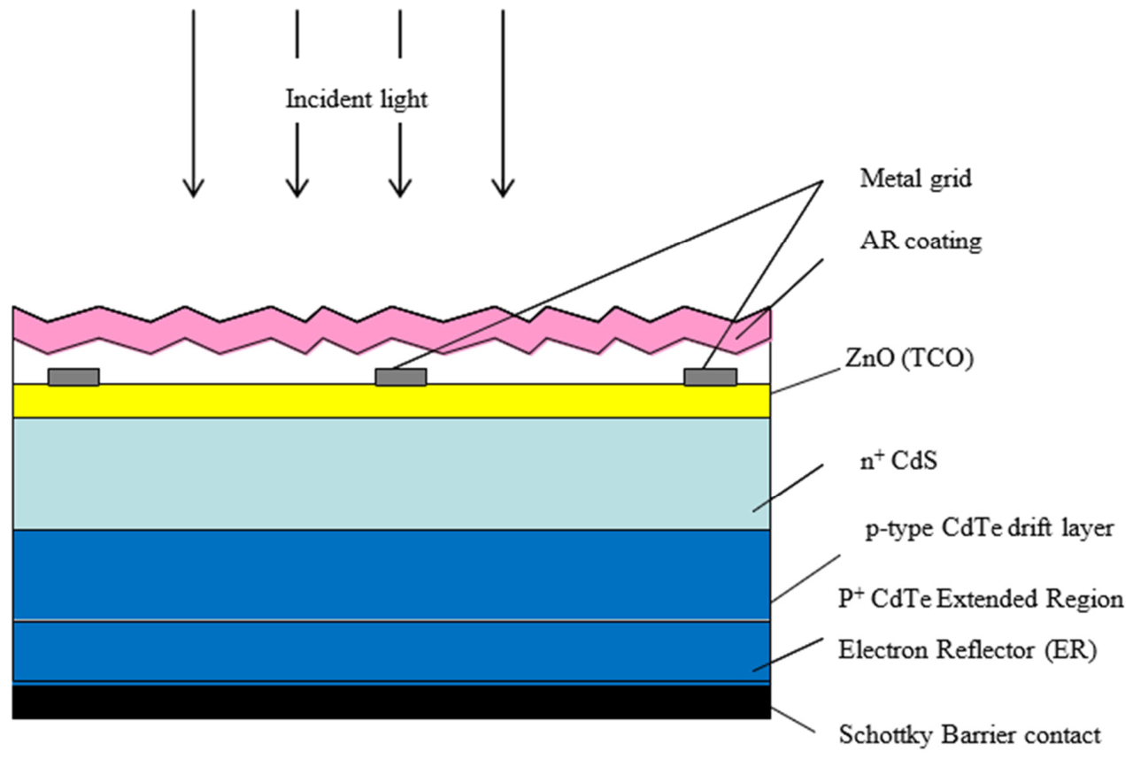
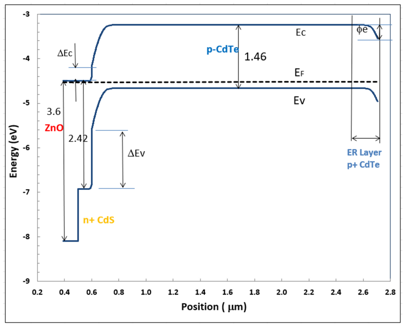
Figure 2.
Simulated illuminated J-V characteristics comparing a higher-work-function, approximately ohmic rear contact (5.45 eV) with a lower-work-function contact (5.05 eV). The main modeled effect is a reduction in the voltage region of the J-V curve, while Jsc changes comparatively little.
Figure 2.
Simulated illuminated J-V characteristics comparing a higher-work-function, approximately ohmic rear contact (5.45 eV) with a lower-work-function contact (5.05 eV). The main modeled effect is a reduction in the voltage region of the J-V curve, while Jsc changes comparatively little.
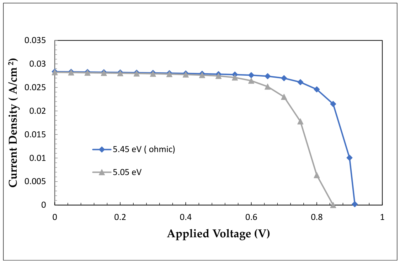
Figure 3.
Simulation of open-circuit voltage as a function of ER thickness. Voc rises from roughly 870 mV at zero ER thickness to about 883 mV at 500 nm in the plotted case.
Figure 3.
Simulation of open-circuit voltage as a function of ER thickness. Voc rises from roughly 870 mV at zero ER thickness to about 883 mV at 500 nm in the plotted case.
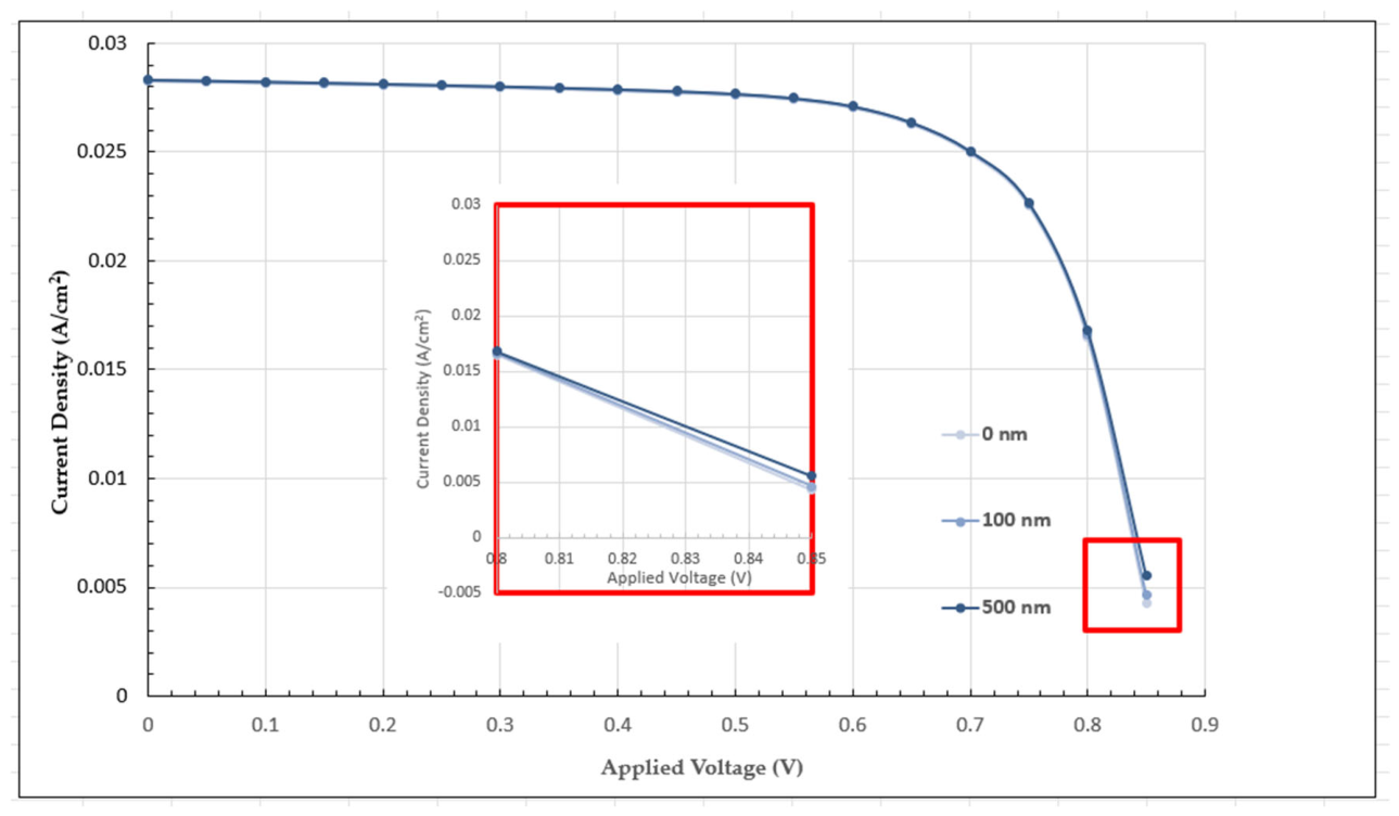
Figure 6.
Optimized-cell result showing power density versus voltage. The reported operating parameters are Voc = 917.6 mV, Jsc = 28.45 mA/cm², and simulated efficiency = 19.83%.
Figure 6.
Optimized-cell result showing power density versus voltage. The reported operating parameters are Voc = 917.6 mV, Jsc = 28.45 mA/cm², and simulated efficiency = 19.83%.
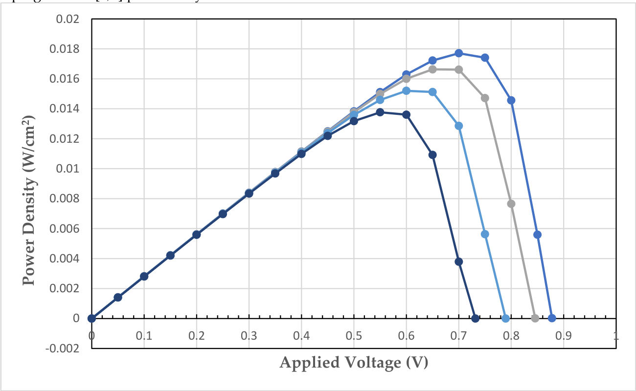

Table 1.
Material parameters used in simulation.
 |
Disclaimer/Publisher’s Note: The statements, opinions and data contained in all publications are solely those of the individual author(s) and contributor(s) and not of MDPI and/or the editor(s). MDPI and/or the editor(s) disclaim responsibility for any injury to people or property resulting from any ideas, methods, instructions or products referred to in the content. |
© 2026 by the authors. Licensee MDPI, Basel, Switzerland. This article is an open access article distributed under the terms and conditions of the Creative Commons Attribution (CC BY) license (http://creativecommons.org/licenses/by/4.0/).
Copyright: This open access article is published under a Creative Commons CC BY 4.0 license, which permit the free download, distribution, and reuse, provided that the author and preprint are cited in any reuse.