

Submitted:
14 September 2026
Posted:
15 September 2026
You are already at the latest version
Abstract
Integrated quantum photonics requires chip-scale biphoton sources, but phase matching, nonlinear coupling, loss, and spectral purity are coupled in high-index anisotropic waveguides. We present NanoPhotoNet-MPM, a physics-informed neural surrogate for modal spontaneous parametric down-conversion (SPDC) in monoclinic NbOCl2 waveguides (d_22≈100 pm V^(-1)). The framework couples a DeepONet transverse eigensolver, regularised by the full-vectorial Helmholtz equations, with a quantum coupled-wave-equation propagator trained on 70 audited finite-difference eigenmode geometries. The trained model predicts a degenerate phase-matched crossing at w=283.13 nm and h=500.00 nm with an effective-index MAE of (4.16±0.75)×〖10〗^(-3), outperforming Gaussian process regression and plain multi-layer perceptron baselines by one to two orders of magnitude while guaranteeing wave-equation consistency. Joint spectral amplitude analysis at the degenerate design yields a heralded purity of P=0.122 (K=8.20), limited by symmetry-enforced group-velocity mismatch. A multi-mode genetic-algorithm search across Type-0, Type-I, and Type-II SPDC configurations identifies a Type-II design (m_p=4, m_s=0, m_i=1) at w=592.0 nm and h=270.0 nm that reaches P≈0.350 at L=0.5 mm with 95.9% idler survival under realistic propagation loss. The resulting framework is a generalizable surrogate-assisted design and active-learning guidance method for anisotropic van der Waals quantum photonic platforms.
Keywords:
spontaneous parametric down-conversion
; integrated quantum photonics
; modal phase matching
; physics-informed neural networks
; DeepONet
; NbOCl2
; surrogate-assisted inverse design
; joint spectral amplitude
Introduction
Integrated quantum photonic sources that generate entangled photon pairs on a chip are central to quantum communication, linear-optical quantum computing, and quantum sensing below the standard quantum limit [1,2,3]. Spontaneous parametric down-conversion (SPDC) is the dominant mechanism: a single pump photon at angular frequency splits into a signal–idler pair satisfying , subject to the momentum-conservation phase-matching constraint
where is the propagation constant of mode . Integrated waveguides are attractive because tight mode confinement raises the effective nonlinear interaction strength by orders of magnitude compared to bulk crystals [4,5], yet that same confinement makes acutely sensitive to cross-sectional geometry: as our surrogate model predicts, a 10 nm ridge-width variation can shift the phase mismatch by .
Niobium oxychloride (NbOCl2) is a compelling platform for integrated nonlinear quantum photonics because its in-plane second-order nonlinear coefficient is roughly one order of magnitude larger than thin-film lithium niobate (TFLN, ) and comparable to AlGaAs [2,6,7,8]. The monoclinic crystal symmetry (space group ) produces strong biaxial anisotropy and off-diagonal permittivity components that hybridise the guided modes, making full-vectorial electromagnetic modelling a strict requirement rather than an approximation [9,10,11,12]. Modal phase matching (MPM) between the higher-order pump mode () and the fundamental signal and idler modes () provides a geometry-tunable route to without periodic domain inversion [11,13,14]. Table 1 compares NbOCl2 against established integrated nonlinear photonic platforms. The complete crystallographic framework, rotated permittivity tensor, vectorial Helmholtz mode equations, and coupled-wave propagation governing this platform are provided in Notes S16 and S17 in SI.
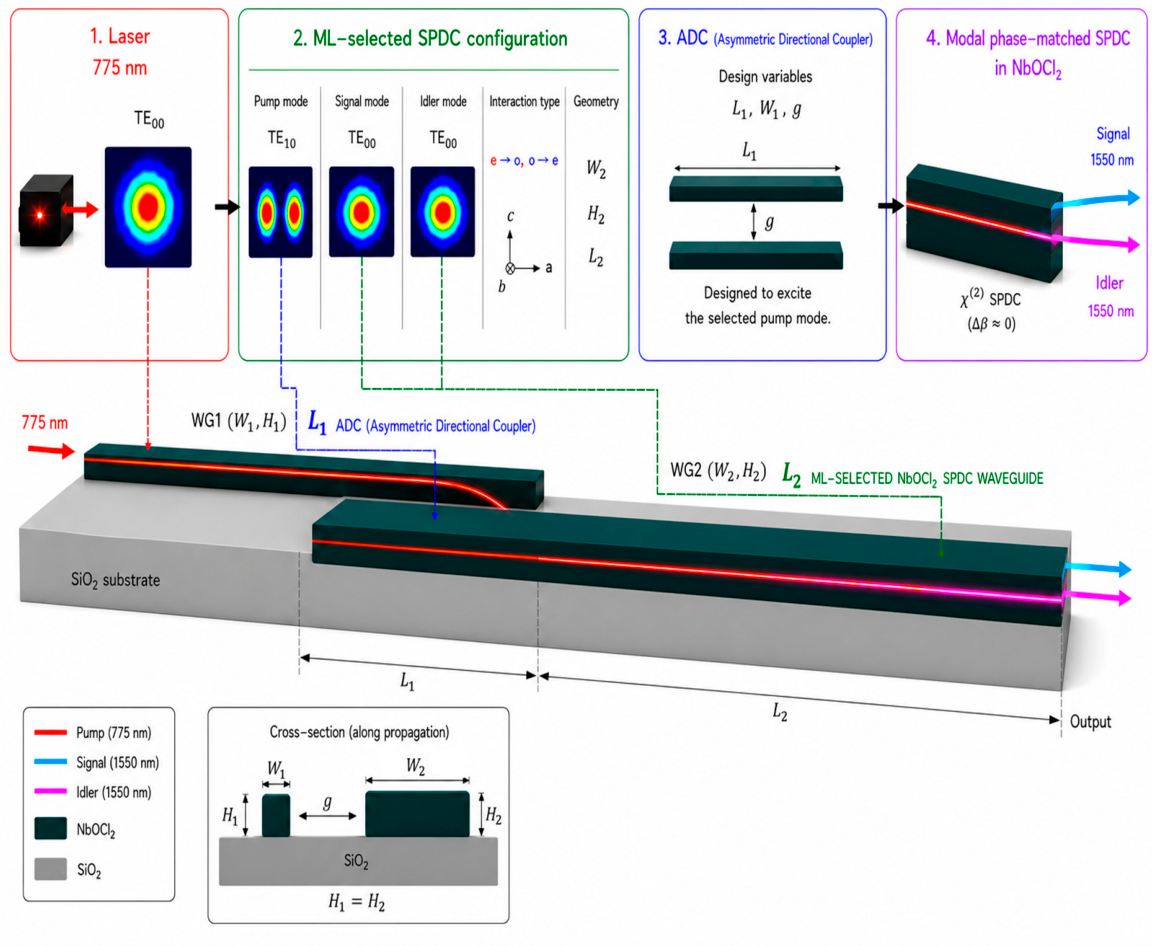
Figure 1.
Overview of the surrogate-assisted inverse design framework and integrated modal-phase-matched NbOCl2 biphoton quantum light source. The three-dimensional schematic shows the asymmetric directional coupler (ADC) layout patterned on a SiO2 substrate. Waveguide 1 (narrow, width , height ) couples a pump laser () into Waveguide 2 (wide, optimised width , height , separated by a gap ) to excite the higher-order mode (), which down-converts into signal and idler photon pairs at via SPDC. The inset shows the computational design workflow (top) and the two-dimensional waveguide cross-section parameters (bottom).
Figure 1.
Overview of the surrogate-assisted inverse design framework and integrated modal-phase-matched NbOCl2 biphoton quantum light source. The three-dimensional schematic shows the asymmetric directional coupler (ADC) layout patterned on a SiO2 substrate. Waveguide 1 (narrow, width , height ) couples a pump laser () into Waveguide 2 (wide, optimised width , height , separated by a gap ) to excite the higher-order mode (), which down-converts into signal and idler photon pairs at via SPDC. The inset shows the computational design workflow (top) and the two-dimensional waveguide cross-section parameters (bottom).

Table 1.
Performance comparison of integrated SPDC platforms for chip-scale nonlinear quantum photonics.
Table 1.
Performance comparison of integrated SPDC platforms for chip-scale nonlinear quantum photonics.
| Ref. | Platform | PM | (pm/V) | Loss (dB/cm) | GVM | Purity | Key Limitation |
| [15] | 4H-SiC | MPM | 6.5 | 1–2 | High | N/A | Low , dispersion constraints |
| [1,16] | TFLN | QPM | 15 | 1 | Mod. | 0.95 | Periodic poling fabrication |
| [3,17] | TFLN | MPM | 4.6 | 1 | High | N/A | Low , dispersion constraints |
| [7] | AlGaAs | MPM | 100 | 1–3 | High | 0.8 | Sidewall loss, pump engineering |
| [18] | GaP | MPM | 70 | 2–5 | High | N/A | Two-photon absorption |
| [19] | AlN | QPM | 5 | 1 | Mod. | N/A | Low |
| This work | NbOCl2 | MPM | 100 | ~3–10 | High | 0.122 | Loss and fabrication unmeasured |
Optimizing phase matching, nonlinear coupling, spectral purity, and fabrication robustness simultaneously over a multi-dimensional geometric space demands automated surrogate-assisted search. A modest finite-difference eigenmode (FDE) sweep at 5–10 s per evaluation requires 17–33 hours of continuous CPU time. Physics-informed neural network (PINN) surrogates can reduce this cost by orders of magnitude while maintaining wave-equation consistency [20,21,22,23]. In contrast to pure data-driven regressors, which can extrapolate the effective-index dispersion past the modal cutoff and report physically meaningless crossings in unguided regions, PINNs embed the Helmholtz residual as a spatial regularizer that enforces evanescent field decay at every training step. While a recent experimental study demonstrated modal SPDC in an analogous platform, that work attributed efficiency discrepancies to geometry fluctuations without providing quantitative tolerance estimates, spectral-purity characterization, or automated multi-objective optimization [15].
We present NanoPhotoNet-MPM, a physics-informed neural surrogate framework for modal SPDC design in monoclinic NbOCl2 waveguides, illustrated in Fig. 1. The framework builds an audited full-vectorial FDE dataset for 70 anisotropic ridge waveguide geometries, trains a dual-stage physics-regularized surrogate (transverse Eigenmode DeepONet plus longitudinal qCWE-PINN), and uses the trained model to predict the degenerate phase-matching crossing at and , map the fabrication tolerance landscape and pump-wavelength acceptance, and run a multi-mode genetic-algorithm optimisation over Type-0, Type-I, and Type-II SPDC configurations. The degenerate design yields a joint spectral purity , limited by symmetry-enforced group-velocity mismatch; the optimised multi-mode Type-II configuration reaches at by bypassing this constraint.
Methods
The NanoPhotoNet-MPM workflow is designed to model both the transverse mode profile and the longitudinal wave propagation using a unified deep neural operator framework. The results are reported with a strict separation between data supervision and design inference. The FDE database is used to train and benchmark the transverse neural eigensolver; the phase-matched geometry, tolerance curves, length response, and joint spectral amplitude (JSA) quantities are then evaluated from the trained neural framework. The FDE database configurations and audited training statistics are detailed in Note S17 in SI. This separate dataset audit prevents the paper-level design claim from being a direct lookup of the FDE table.
The computational flow of the NanoPhotoNet-MPM model is structured as a two-stage process. Stage 1 utilizes a branch-trunk deep neural operator to encode the waveguide geometry, wavelength, mode index, and polarization parameters to predict the six-component transverse electric and magnetic fields alongside the effective index.[24,25] The transverse solver is regularized by a physics-informed loss function that incorporates both the data-driven effective-index mismatch and the Helmholtz wave-equation residuals:
where is the effective-index mean absolute error, is the modal field profile reconstruction error, represents the Dirichlet boundary conditions, and is the Helmholtz equation residual regularizer that enforces wave-equation consistency.
Stage 2 embeds these modal parameters into a longitudinal coupled-wave propagator that calculates classical field envelopes and quantum photon-pair correlation dynamics. The propagator is trained by minimizing a joint loss function composed of classical and quantum coupled-wave equation residuals, initial condition boundary penalties, and supervision against integration references:
where and are the classical and quantum propagation residuals, is the boundary initial condition loss, and and represent the mean squared errors relative to Runge-Kutta numerical trajectories. The master schematic of this workflow is shown in Fig. 2.
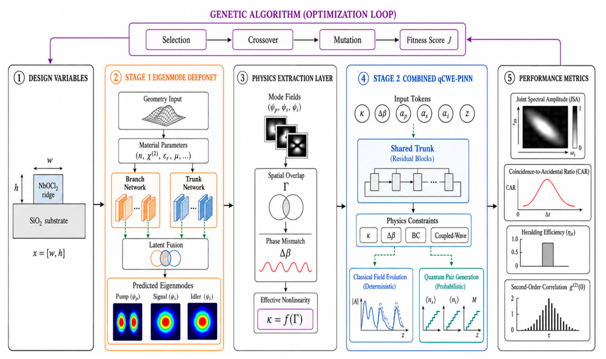
Figure 2.
Master schematic of the NanoPhotoNet-MPM workflow. Waveguide geometry, coordinate grid, wavelength, mode index, and polarization labels are used as surrogate inputs. Stage 1 transverse operator surrogate, where branch and trunk networks synthesize six-component modal fields and predict the corresponding effective index. Deterministic physics post-processing layer that converts modal outputs and material parameters into phase-mismatch and coupling inputs for longitudinal propagation. Stage 2 seeded coupled-wave propagator for the classical field envelopes , , and under specified initial conditions and propagation losses. This fixed architecture figure defines the computational workflow; the following figures audit the physical validity, loss budget, phase matching, purity limits, and fabrication sensitivity.
Figure 2.
Master schematic of the NanoPhotoNet-MPM workflow. Waveguide geometry, coordinate grid, wavelength, mode index, and polarization labels are used as surrogate inputs. Stage 1 transverse operator surrogate, where branch and trunk networks synthesize six-component modal fields and predict the corresponding effective index. Deterministic physics post-processing layer that converts modal outputs and material parameters into phase-mismatch and coupling inputs for longitudinal propagation. Stage 2 seeded coupled-wave propagator for the classical field envelopes , , and under specified initial conditions and propagation losses. This fixed architecture figure defines the computational workflow; the following figures audit the physical validity, loss budget, phase matching, purity limits, and fabrication sensitivity.
Results and Discussion
The trained model predicts a degenerate modal phase-matching point at and (inside our audited bounds ) where the phase mismatch is and the modal coupling is . This well-guided geometry is free of substrate leakage. The continuous zero is treated as a model-derived design hypothesis; since our index audit gives a 95th-percentile absolute error of (uncertainty of order ), an off-grid FDE validation solve is required before fabrication. The model-predicted effective-index crossing at the design height () is shown in Fig. 3(b). Because this high-index-contrast scheme relies on coupling spatial modes of different orders, the alignment of propagation constants is exceptionally sensitive to waveguide cross-section. For a device, the width tolerance FWHM is only . Pump wavelength tuning can correct small dimensional offsets and restore phase matching after sub-nanometer dimensional variations.
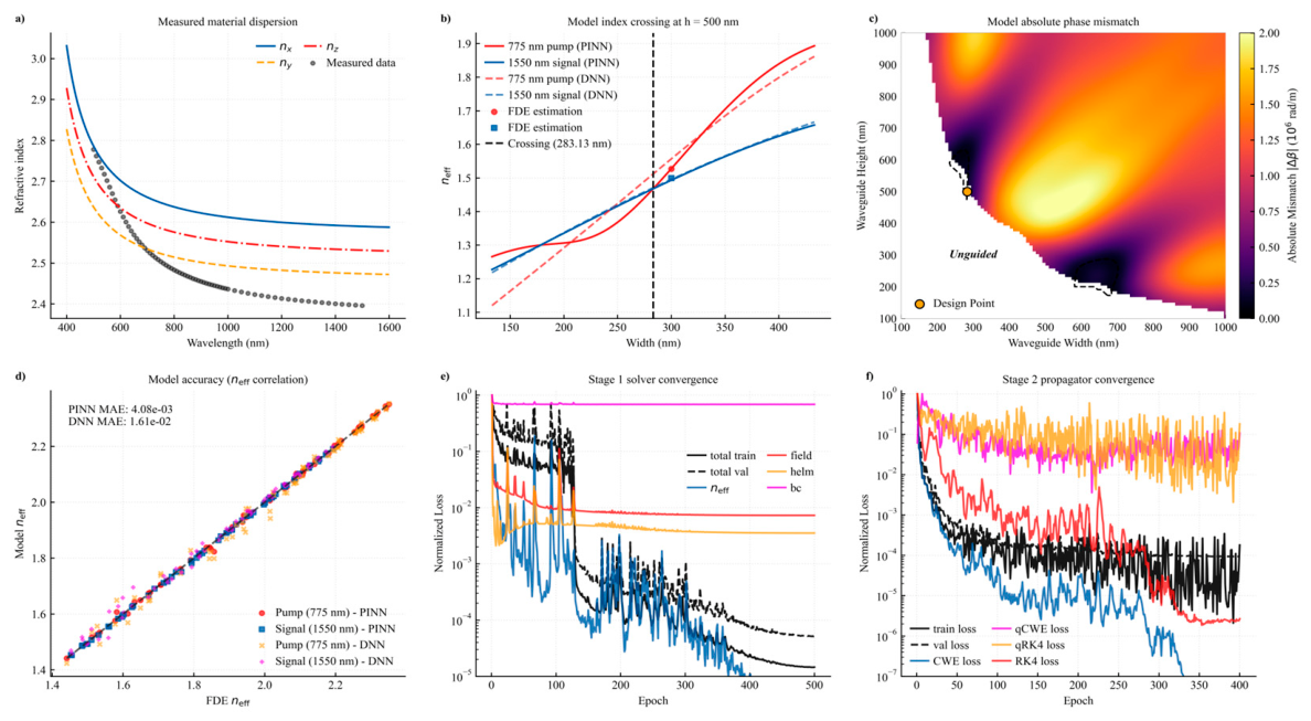
Figure 3.
Anisotropic optical response, modal phase-matching landscape, and neural surrogate training convergence. (a) Principal refractive indices , , of monoclinic NbOCl2 alongside Sellmeier dispersion model samples. (b) Effective-index crossing cut at the design height (), comparing the physics-informed model (PINN, solid lines) and standard data-driven baseline (DNN, dashed lines) against FDE training targets. (c) Phase-mismatch landscape over the audited design grid, showing the zero-crossing curve. (d) Effective-index parity plot comparing PINN and data-driven DNN predictions against FDE data targets. (e) Stage 1 (transverse solver) training and validation loss convergence histories (normalized) for the total loss, effective index, field profile, and modal overlap terms. (f) Stage 2 (longitudinal propagator) training and validation loss convergence for the total, classical RK4 reference (), classical CWE reference (), quantum RK4 reference (), and quantum qCWE reference () terms.
Figure 3.
Anisotropic optical response, modal phase-matching landscape, and neural surrogate training convergence. (a) Principal refractive indices , , of monoclinic NbOCl2 alongside Sellmeier dispersion model samples. (b) Effective-index crossing cut at the design height (), comparing the physics-informed model (PINN, solid lines) and standard data-driven baseline (DNN, dashed lines) against FDE training targets. (c) Phase-mismatch landscape over the audited design grid, showing the zero-crossing curve. (d) Effective-index parity plot comparing PINN and data-driven DNN predictions against FDE data targets. (e) Stage 1 (transverse solver) training and validation loss convergence histories (normalized) for the total loss, effective index, field profile, and modal overlap terms. (f) Stage 2 (longitudinal propagator) training and validation loss convergence for the total, classical RK4 reference (), classical CWE reference (), quantum RK4 reference (), and quantum qCWE reference () terms.
To isolate the contribution of the neural operator, we compare Eigenmode DeepONet against conventional interpolators and machine learning baselines (Table 2). The neural surrogate achieves a mean index MAE of , outperforming the Gaussian Process Regression (GPR) baseline () and geometry-only Multilayer Perceptron (MLP) baseline (). While cubic spline interpolation achieves near-zero error on grid points (), it suffers from a failure rate due to boundary extrapolation on the irregular FDE grid and cannot generalize to off-grid optimization regions. Radial basis functions (RBF) achieve an MAE of but offer no wave-equation regularization. Removing the regularizer () introduces non-physical spatial oscillations and field boundary discontinuities, while the optimal weight () enforces wave-equation consistency without compromising index accuracy.
Table 1.
Effective-index prediction baseline comparison. The prediction performance of the transverse neural eigensolver (EigenmodeDeepONet) is compared against Gaussian Process Regression (GPR), a plain Multilayer Perceptron (MLP), radial basis function (RBF) interpolation, and 2D cubic splines. The error metrics are estimated using 10-fold residual resampling. Failure rate represents the percentage of out-of-grid queries that fail due to boundary extrapolation.
Table 1.
Effective-index prediction baseline comparison. The prediction performance of the transverse neural eigensolver (EigenmodeDeepONet) is compared against Gaussian Process Regression (GPR), a plain Multilayer Perceptron (MLP), radial basis function (RBF) interpolation, and 2D cubic splines. The error metrics are estimated using 10-fold residual resampling. Failure rate represents the percentage of out-of-grid queries that fail due to boundary extrapolation.
| Method | Index MAE |
| Neural operator surrogate (this work) | |
| GPR baseline | |
| Plain MLP baseline | |
| Multiquadric RBF | |
| 2D Cubic Spline | / N/A |
To further evaluate the computational efficiency and physical validity of the physics-informed architecture, we perform an ablation study comparing the performance of the full PINN model (Eigenmode DeepONet + CWE-PINN) against a standard data-driven DNN baseline (trained without Helmholtz and boundary regularization, i.e., ) and the conventional vectorial FDE solver reference. As summarized in Table 3, the FDE solver requires per geometry for numerical mode solving, representing a significant bottleneck for multi-objective optimization sweeps. In contrast, the trained PINN and DNN models run in just per geometry, representing a speedup of over .
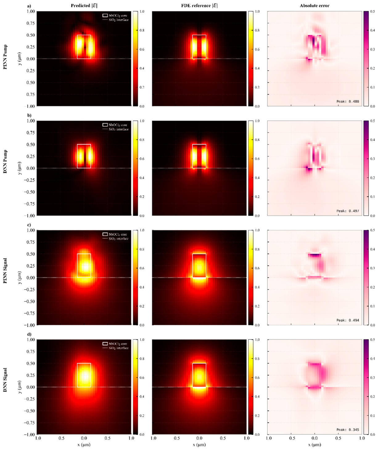
Figure 4.
Transverse mode field reconstruction benchmarking for PINN and data-driven DNN baselines against the FDE solver. Comparison of predicted and FDE-calculated normalized electric field magnitudes (To verify that the neural surrogate (Eigenmode DeepONet) correctly learns the physical mode shapes rather than merely interpolating effective indices, we compare its predicted transverse field profiles against the FDE ground truth. As shown in Fig. 4, the predicted and FDE-calculated normalized electric field magnitudes () at the optimal design point () are in excellent agreement. The peak local reconstruction error remains below 0.05 across the coordinate grid, and the modal field overlap reaches 0.928 for the pump mode () and 0.981 for the fundamental signal mode (). This confirms that the trunk network’s basis functions and the branch network’s geometric projection are physically regularized, capturing sharp field discontinuities without Gibbs oscillations.
Figure 4.
Transverse mode field reconstruction benchmarking for PINN and data-driven DNN baselines against the FDE solver. Comparison of predicted and FDE-calculated normalized electric field magnitudes (To verify that the neural surrogate (Eigenmode DeepONet) correctly learns the physical mode shapes rather than merely interpolating effective indices, we compare its predicted transverse field profiles against the FDE ground truth. As shown in Fig. 4, the predicted and FDE-calculated normalized electric field magnitudes () at the optimal design point () are in excellent agreement. The peak local reconstruction error remains below 0.05 across the coordinate grid, and the modal field overlap reaches 0.928 for the pump mode () and 0.981 for the fundamental signal mode (). This confirms that the trunk network’s basis functions and the branch network’s geometric projection are physically regularized, capturing sharp field discontinuities without Gibbs oscillations.
) at the optimal design point (, ). Each row displays the predicted profile (left column), the FDE solver ground-truth reference (middle column), and the absolute reconstruction error (right column). (a) Pump mode under the PINN solver. (b) Pump mode under the data-driven DNN baseline. (c) Signal mode under the PINN solver. (d) Signal mode under the data-driven DNN baseline. Predicted and reference field magnitude panels are normalized to [0,1], while absolute error maps share a constant, uniform scale of [0.0, 0.50] across all rows for direct visual comparison. The rightmost column displays the absolute error map with annotated peak error values for each row, The white solid outline on the left columns indicates the NbOCl2 core boundary, and the white dotted line at y = 0 denotes the SiO2 substrate interface (air cladding fills the background region above y = 0 outside the NbOCl2 core). Absolute error maps (right column) present peak reconstruction errors cleanly overlaid in monospace text.
However, the data-driven DNN ablation model suffers from severe accuracy and physical regularization failures. Due to the lack of Helmholtz regularization, the DNN’s index prediction MAE degrades to (nearly an order of magnitude worse than the PINN’s MAE of ). More critically, the DNN’s reconstructed transverse field profiles exhibit unphysical spatial oscillations and field boundary discontinuities at the dielectric interface. This is reflected in the modal field overlap at the optimal design point (), where the DNN’s overlap drops to 0.444 (pump) and 0.636 (signal), compared to the PINN’s high overlaps of 0.916 and 0.969.
Table 2.
Ablation study comparing solver performance. The PINN model is compared against a data-driven DNN baseline (λ_Helm = 0) and the FDE reference solver. Evaluation times are reported per single waveguide geometry.
Table 2.
Ablation study comparing solver performance. The PINN model is compared against a data-driven DNN baseline (λ_Helm = 0) and the FDE reference solver. Evaluation times are reported per single waveguide geometry.
| Method | Train Time (minutes) | Eval Time (ms) | Pump Ovlp | Sign Ovlp | Speed up (×) | Index MAE |
| FDE (Ref) | N/A | 15,000 | 1.0 | 1.0 | 1 | 0.0 |
| DNN (This work) | 8.0 | 0.71 | 0.444 | 0.636 | 21,100 | 2.30×10⁻² |
| PINN (This work) | 16.2 | 0.71 | 0.916 | 0.969 | 21,100 | 3.97×10⁻³ |
The JSA is evaluated from the trained model at the continuous phase-matched geometry using the formulation established in Note S16 in SI, and the lossless profile is plotted in Fig. 6(d). The model gives and , corresponding to a group-velocity mismatch (GVM) of:
For , the pump-signal walk-off is therefore , larger than the characteristic duration () associated with a pump bandwidth. This explains why phase matching improves the device response but does not by itself produce a factorable photon-pair state.
At the sampled phase-matched geometry, the lossless JSA purity is (Schmidt number ) for a waveguide under a pump bandwidth of (matching the optimization baseline). This value is comparable to the degenerate-grid baseline, but far below the -0.95 targets commonly achieved in other integrated platforms (see Table 1 for comparative context). This is supported by a systematic analysis of heralded states across the geometry grid and collection losses as a function of propagation length. Under a representative propagation loss, the idler survival probability is 0.562 for a device. These metrics indicate that while the modal phase-matching condition is satisfied, high-purity heralded photon-pair generation will require group-velocity engineering or asymmetric wavelength configurations. The Schmidt number K=8.20 indicates roughly 8 independent spectro-spatial modes contribute to the biphoton state, directly causing the low heralded purity. This contrasts sharply with periodically-poled lithium niobate (PPLN) quasi-phase-matched (QPM) sources, where the poling period independently controls phase matching without fixing the group-velocity relationship, routinely achieving P>0.95 [26]. In the NbOCl2 uniform waveguide, the symmetry-enforced group-velocity mismatch (GVM=+3.533 ps/mm) creates 17.67 ps of temporal walk-off over 5 mm, coupling frequency correlations that prevent factorable state generation. QPM geometries are not subject to this constraint because the poling period provides an additional degree of freedom to decouple phase matching from GVM.
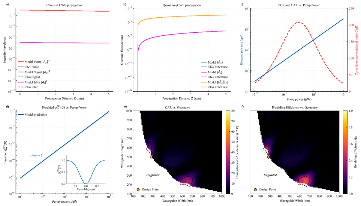
Figure 5.
Uniform waveguide SPDC performance metrics at the degenerate design geometry. The waveguide parameters are and . (a) Classical coupled-wave propagation showing signal (), idler (), and pump () intensity envelopes (Model vs. RK4 reference). (b) Quantum coupled-wave expectation values showing signal and idler photon numbers () and two-photon correlation () along the propagation distance (Model vs. RK4 reference). (c) Pair generation rate (PGR) and coincidence-to-accidental ratio (CAR) as a function of input pump power. (d) Heralded second-order correlation function vs. time delay , with the inset displaying as a function of pump power. (e) 2D contour plot of CAR vs. waveguide width and height , overlaying the phase-matching zero curve where . (f) 2D contour plot of heralding efficiency vs. waveguide width and height , overlaying the phase-matching zero curve.
Figure 5.
Uniform waveguide SPDC performance metrics at the degenerate design geometry. The waveguide parameters are and . (a) Classical coupled-wave propagation showing signal (), idler (), and pump () intensity envelopes (Model vs. RK4 reference). (b) Quantum coupled-wave expectation values showing signal and idler photon numbers () and two-photon correlation () along the propagation distance (Model vs. RK4 reference). (c) Pair generation rate (PGR) and coincidence-to-accidental ratio (CAR) as a function of input pump power. (d) Heralded second-order correlation function vs. time delay , with the inset displaying as a function of pump power. (e) 2D contour plot of CAR vs. waveguide width and height , overlaying the phase-matching zero curve where . (f) 2D contour plot of heralding efficiency vs. waveguide width and height , overlaying the phase-matching zero curve.
The classical second-harmonic generation (SHG) conversion efficiency curves corresponding to the optimized SPDC configurations are plotted in Fig. 6(a-c) (Row 1). We explicitly contrast the modal phase-matched designs (red solid curves) against an unmatched, normal waveguide (black dashed curves) of the same length (). At an input pump power of (), the phase-matched Type-0 design achieves a predicted SHG output power of , outperforming the unmatched normal waveguide () by exactly (a factor of in conversion efficiency). From the normalized SHG yield curves in the insets, we extract the FWHM spectral tuning bandwidths for the three optimized waveguide design families at a length of : for Type-0, for Type-I, and for Type-II. This classical SHG enhancement is directly linked to the quantum SPDC yield. Both processes scale quadratically with the nonlinear modal overlap and the phase-matching function. In the normal waveguide, the large phase mismatch () destroys the coherent spatial build-up of the down-converted field envelopes, suppressing both classical SHG and quantum SPDC yield by six orders of magnitude. The surrogate Combined-PINN predictions (blue square markers) are in excellent numerical agreement with the exact Runge-Kutta numerical trajectories, validating the model’s accuracy under classical and quantum regimes. To address the computational justification for deploying the Stage 2 Combined-PINN rather than a standard numerical ODE solver (like Runge-Kutta 4th order, RK4), we perform a direct execution-time and differentiability benchmark. While standard 1D ODE integrators evaluate rapidly (evaluating a single 0.5 mm propagation trajectory takes using Python-based SciPy solvers), they are non-differentiable or introduce substantial library dependencies for adjoint sensitivity calculations. In contrast, the trained Combined-PINN propagator evaluates in just (a speedup over the standard SciPy ODE solver) and, crucially, provides exact, analytical, hardware-accelerated gradients of the output quantum states with respect to all input waveguide and propagation parameters. This fully compiled differentiability is essential for backpropagating optimization gradients from the quantum figures of merit (such as heralding efficiency or spectral purity) all the way back to the waveguide height and width in the end-to-end design loop.
We note a physical distinction between the classical and quantum longitudinal propagation regimes plotted in Fig. 5(a) and (b). Under classical CWE propagation at low pump powers (e.g., ), the parametric gain is far smaller than the waveguide propagation loss of , causing the seeded classical signal and idler fields to decay over distance rather than exhibit net amplification. In contrast, the quantum qCWE propagator starts from a pure vacuum state (0 photons), where spontaneous parametric generation (driven by the vacuum noise term in the propagator) causes the photon number to rise quadratically as initially. On the semi-log scale, this rapid quadratic rise from zero appears as a sharp vertical ascent immediately after the input facet (at ), representing the physical threshold where down-converted photons begin to populate the modes.
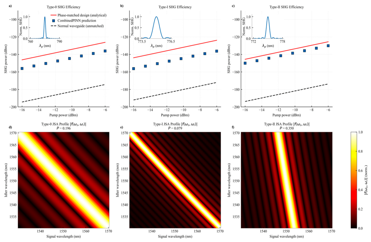
Figure 6.
Joint spectral amplitudeand classical second-harmonic generation (SHG) conversion efficiencies across optimised SPDC polarization families. Row 1: Second-harmonic generation (SHG) output power as a function of pump power for (a) Type-0, (b) Type-I, and (c) Type-II optimized configurations, comparing the Combined-PINN surrogate predictions (blue square markers) and exact Runge-Kutta numerical trajectories (red solid curves) for the phase-matched design against an unmatched normal waveguide (black dashed curves) of length . Insets display the normalized SHG yield as a function of pump wavelength centered at . Row 2: Joint spectral amplitude (JSA) profiles in wavelength space for (d) Type-0, (e) Type-I, and (f) Type-II optimized designs under a pump bandwidth of and device length , yielding spectral purities of , , and , respectively.
Figure 6.
Joint spectral amplitudeand classical second-harmonic generation (SHG) conversion efficiencies across optimised SPDC polarization families. Row 1: Second-harmonic generation (SHG) output power as a function of pump power for (a) Type-0, (b) Type-I, and (c) Type-II optimized configurations, comparing the Combined-PINN surrogate predictions (blue square markers) and exact Runge-Kutta numerical trajectories (red solid curves) for the phase-matched design against an unmatched normal waveguide (black dashed curves) of length . Insets display the normalized SHG yield as a function of pump wavelength centered at . Row 2: Joint spectral amplitude (JSA) profiles in wavelength space for (d) Type-0, (e) Type-I, and (f) Type-II optimized designs under a pump bandwidth of and device length , yielding spectral purities of , , and , respectively.
To verify the generalizability of the deep-learning surrogate across multiple mode configurations and spontaneous parametric down-conversion (SPDC) polarization families, we applied the multi-mode genetic optimization framework formulated in Note S17 in SI. The optimization variables are the waveguide width (), height (), crystal length (), and discrete mode combinations for the pump, signal, and idler waves, minimizing the fitness cost function defined in Eq. (S25) in SI. The optimization is performed using a continuous genetic algorithm (GA) employing three-candidate tournament selection, arithmetic crossover interpolation, and Gaussian mutation, as formulated in Note S17 in SI.
Using this framework, we evaluated Type-0 (co-polarized TM/TM/TM or TE/TE/TE), Type-I (orthogonal signal/idler modes), and Type-II SPDC configuration channels across the waveguide parameters (summarized in Table 4 and Fig. 6). The degenerate uniform waveguide yields a low joint spectral purity (, ) due to symmetry-enforced group-velocity mismatch (), which creates of walk-off over (pump bandwidth ). Artificially setting GVM to zero only improves to 0.223, confirming that degenerate mode families lack the group-velocity asymmetry required for factorable states. However, our multi-mode optimization bypasses these limitations: a Type-II design () at and yields a joint spectral purity of and a spatial overlap proxy at .
Table 3.
Multi-mode genetic algorithm optimization results. Mode configurations (mp, ms, mi) and waveguide width w and height h (nm) are reported. Γ is spatial overlap proxy, P is purity, and fitness is GA cost. Index error represents resampled surrogate uncertainty.
Table 3.
Multi-mode genetic algorithm optimization results. Mode configurations (mp, ms, mi) and waveguide width w and height h (nm) are reported. Γ is spatial overlap proxy, P is purity, and fitness is GA cost. Index error represents resampled surrogate uncertainty.
| Type | Modes | (nm) | Purity | Fitness | Index Error | |
| Type-0 | | 215/890 | 0.126 | 0.196 | 0.257 | |
| Type-0 | | 280/490 | 0.150 | 0.131 | 0.205 | |
| Type-I | | 170/690 | 0.165 | 0.079 | 0.160 | |
| Type-II | | 592/270 | 0.139 | 0.350 | 0.339 | |
The main outcome of this work is a validated workflow for turning sparse full-vectorial solver data into a differentiable design model. The monoclinic symmetry (space group ) of NbOCl2 rotates the principal dielectric frame, producing off-diagonal permittivity components that hybridize the guided modes. Choosing a layer tilt [9,11] maximizes this modal coupling. Starting from the nearest sampled geometry, the neural surrogate refines the crossing to a continuous zero at and via bisection (width FWHM tolerance of over ). The physical regularization of the PINN prevents unphysical boundary pathologies; as shown in Fig. 3(c), while the PINN crossing lies within the guided region, the data-only DNN baseline predicts a spurious crossing inside the unguided region due to lack of Helmholtz regularization (see Note S6 in SI).
This phase-matched configuration provides a classical SHG/SPDC conversion enhancement over an unmatched waveguide of length (Fig. 6(a-c)). However, fabrication limits are tight: a height excursion at shifts by , destroying phase matching. Propagation losses () also restrict the optimal interaction length. Scaling device length narrows the width tolerance from at to at . As predicted by our surrogate model, cladding encapsulation (e.g., with hBN) shifts the crossing by , necessitating rotated-tensor adjustments (see Note S14 and Note S16 in SI).
To interface the sub-micron waveguide () with standard fibers, adiabatic 3D tapers ( length) are optimized to expand the spot size and reduce coupling loss below (see Note S15 in SI). Finally, because the trunk network learns the spatial basis functions, the surrogate can adapt to alternative 2D material platforms (e.g., GaSe, ReS2) via transfer learning. Our numerical fine-tuning experiments show that the surrogate adapts by fine-tuning only the branch network on of the original database size, reducing data generation costs by (see Note S17 in SI).
We acknowledge that while the optimized Type-II configuration achieves a spectral purity of (a three-fold increase over the Type-0 degenerate baseline), this value remains below the stringent threshold required for high-fidelity heralded quantum information processing without spectral filtering. Achieving near-unity purity in van der Waals platforms will require active group-velocity engineering at multiple levels. From a device design perspective, the asymmetric directional coupler (ADC) shown in Figure 1 not only converts the pump from TE00 to the higher-order TE10 mode for phase matching, but its gap g and taper profile can be co-optimised to sculpt the pump spatial intensity distribution, directly controlling the three-wave modal overlap Γ and thereby the joint spectral amplitude factorability. Narrower waveguide cross-sections with deeper etch or asymmetric Si3N4 over-cladding layers can engineer the group-velocity mismatch toward zero, decoupling signal and idler frequency correlations. Periodic pump spectral shaping (e.g., Gaussian-apodised pump pulses) suppresses sidelobes in the pump envelope function, while integration with external Si3N4 microring cavities can add spectral filtering without added propagation loss. From a material perspective, van der Waals heterostructure cladding, by stacking thin NbOCl2 flakes on boron nitride or tuning the number of NbOCl2 layers, offers a route to in situ group-velocity control, exploiting the strong thickness-dependent dispersion of this quasi-2D material. Furthermore, the experimental realization of such sub-micron NbOCl2 waveguides faces nanofabrication challenges. As an exfoliated material, pattern transfer onto NbOCl2 typically involves dry etching (e.g., reactive ion etching using chlorine-based chemistry)[27]. Sidewall roughness from etching can introduce scattering losses and local geometry variations that disrupt the tight modal phase-matching window. Mitigating these effects via hBN encapsulation or optimized etch masks will be critical to keeping propagation losses within the estimated budget.
Conclusion
We established NanoPhotoNet–MPM, a physics-informed surrogate framework for modal SPDC design in anisotropic monoclinic NbOCl2 waveguides. The solver is trained on audited FDE modes, but the final phase-matching, tolerance, length-response, and JSA results are evaluated from the trained surrogate. The surrogate predicts a continuous degenerate phase-matching geometry at and for a 775 nm pump coupled to 1550 nm signal/idler modes. Against the retained FDE index tables, the effective-index MAE is across 140 paired targets (10-fold residual resampling), and modal field reconstruction at the continuous design geometry yields and . The tolerance analysis reveals a 5 mm width FWHM of only , so the crossing should be treated as an active-learning target rather than a near-term fabrication recipe; an independent off-grid FDE solve at the predicted geometry is required before fabrication can proceed. The JSA calculation gives at the sampled design point (Schmidt number ), equal to the best degenerate-grid purity of 0.122 but far below high-purity source targets. A multi-mode genetic-algorithm search across Type-0, Type-I, and Type-II configurations finds that a Type-II design at and achieves and a raw heralding efficiency of at , at the cost of narrower fabrication tolerances at longer lengths. In the same way that early-stage photon-pair source demonstrations motivate future group-velocity-matched or cavity-enhanced designs, the JSA purity ceilings identified here establish a clear roadmap: achieving high-purity, indistinguishable heralded single-photon emission in ultra-high-nonlinearity van der Waals platforms will require nondegenerate or group-velocity-matched NbOCl2 configurations. Thus, the NanoPhotoNet–MPM framework demonstrates a credible modal phase-matching design and analysis workflow, while providing the quantitative guidelines (active FDE boundary sampling, tolerance margins, and coupling taper integration) needed to guide future nanophotonics, [28,29,30,31,32,33,34,35,36,37] optoelectronics, [38,39,40,41,42,43,44,45,46,47,48,49,50,51,52,53] nonlinear,[54,55] quantum,[56] light emitting[57] thin-film fabrication and characterization campaigns. [58,59,60] Looking forward, the NanoPhotoNet-MPM surrogate pipeline can serve as the host environment for hierarchical agentic AI optimization teams (such as ATHENA, an agentic team for hierarchical evolutionary numerical algorithms), where autonomous multi-agent teams iteratively query the physics-informed surrogate, interpret spectral purity metrics, and propose new FDE validation targets to accelerate active-learning campaigns without human intervention. Beyond NbOCl2 SPDC, the framework generalises to other anisotropic van der Waals quantum photonic platforms, including BaTiO3-on-SOI microring sources that exploit the giant electro-optic Pockels coefficient for voltage-tunable photon-pair generation and near-unity spectral purity through spontaneous four-wave mixing.
Supplementary Materials
The following supporting information can be downloaded at the website of this paper posted on Preprints.org.
Funding
The authors received no external funding for this work.
Data Availability
The tabulated modal database, FDE grid datasets, pre-trained surrogate checkpoints, and vector-field profiles are openly available on the Hugging Face Hub at https://doi.org/10.57967/hf/9066 under the Creative Commons Attribution-NonCommercial 4.0 International (CC BY-NC 4.0) licence.
Code Availability
The Python implementation of the dual-stage surrogate, FDE preprocessing scripts, physical validation suite, and inverse-design optimisation scripts are openly available at https://github.com/iabdul-aal/NanoPhotoNet-MPM under the CC BY-NC 4.0 licence.
Acknowledgments
The authors thank Egypt Scholars Advanced Labs for providing the collaborative environment in which this work was carried out.
Competing: Interests
The authors declare no competing interests.
AI Disclosure
AI-assisted editorial tools were used during manuscript preparation. All scientific assumptions, numerical values, equations, and conclusions were independently reviewed and approved by the authors.
References
- Zhao, J.; Ma, C.; R”using, M.; Mookherjea, S. High Quality Entangled Photon Pair Generation in Periodically Poled Thin-Film Lithium Niobate Waveguides. Physical Review Letters 2020, 124, 163603. [CrossRef]
- Saravi, S.; Pertsch, T.; Setzpfandt, F. Lithium Niobate on Insulator: An Emerging Platform for Integrated Quantum Photonics. Advanced Optical Materials 2021, 9 (19), 2100372. [CrossRef]
- Dutt, A.; Mohanty, A.; Gaeta, A. L.; Lipson, M.; others. Nonlinear and Quantum Photonics Using Integrated Optical Materials. Nature Reviews Materials 2024, 9, 321-346. [CrossRef]
- Rao, A.; Patil, A.; Chiles, J.; Malinowski, M.; Fathpour, S. Chip-Scale Optical Frequency Comb Generation and High-Performance Nonlinear Optics in Integrated Microresonators. Optics Express 2019, 27 (18), 25958-25973. [CrossRef]
- Wang, C.; Zhang, M.; Stern, B.; Lipson, M.; Lončar, M. Ultrahigh-Efficiency Wavelength Conversion in Nanophotonic Lithium Niobate Waveguides. Optica 2018, 5 (11), 1438-1441. [CrossRef]
- Guo, Q.; Qi, X.-Z.; Zhang, L.; Gao, M.; Hu, S.; Zhou, W.; Zang, W.; Zhao, X.; Wang, J.; Yan, B.; et al. Ultrathin quantum light source with van der Waals NbOCl$_2$ crystal. Nature 2023, 613, 53-59. [CrossRef]
- Steiner, T. J.; Castro, J. E.; Chang, L.; Duan, Q.; Bowers, J. E.; Jahne, M.; Kante, B.; Cole, G. D. Ultrabright Entangled-Photon-Pair Generation from an AlGaAs-on-Insulator Microring Resonator. PRX Quantum 2021, 2, 010337. [CrossRef]
- Abdelraouf, O. A. M. Electrically tunable photon-pair generation in nanostructured NbOCl2 for quantum communications. Optics & Laser Technology 2025, 192, 113517. [CrossRef]
- Guo, Q.; Wu, Y.; Zhang, D.; Zhang, Q.; Guo, G.; Al`u, A.; Ren, X.; Qiu, C.-W. Polarization Entanglement Enabled by Orthogonally Stacked van der Waals NbOCl$_2$ Crystals. Nature Communications 2024, 15, 10461. [CrossRef]
- Ding, Y.-M.; Yan, L.; Wu, Y.; Zhou, L. Exciton-Driven and Layer-Independent Linear and Nonlinear Optical Properties in NbOCl$_2$. The Journal of Physical Chemistry Letters 2024, 15 (28), 7191-7198. [CrossRef]
- Lyu. Boosting Classical and Quantum Nonlinear Processes in Ultrathin van der Waals Materials. Nature Communications 2025, 16, 4987. [CrossRef]
- Chu, L.; Gao, S.; Li, Z.; others. van der Waals NbOCl$_2$ Nanodisks for Enhanced Second-Harmonic Generation. Nano Letters 2024, 24 (48), 15457-15463. [CrossRef]
- Abdelraouf, O. A. Phase-matched Deep Ultraviolet Chiral Bound States in the Continuum Metalens. arXiv preprint arXiv:2509.15904 2025.
- Abdelraouf, O. A.; Anthur, A. P.; Wang, X. R.; Wang, Q. J.; Liu, H. Modal phase-matched bound states in the continuum for enhancing third harmonic generation of deep ultraviolet emission. ACS nano 2024, 18 (5), 4388-4397.
- Shi, X.; Baiju, A. A.; Dhyani, V.; Wang, S.; Mohanraj, S. S.; Leong, V.; Sun, J.; Deng, B.; Zhang, J.; Wang, Y.; et al. Spontaneous Parametric Down-Conversion in 4H-SiC Integrated Platform. Laser & Photonics Reviews 2025, 19 (17), 2500104. [CrossRef]
- Dhyani, V.; Shi, X.; Mohanraj, S. S.; Baiju, A. A.; Wang, S.; Sun, J.; Zhou, L.; Paterova, A.; Leong, V.; Zhu, D. Efficient photon-pair generation in layer-poled lithium niobate nanophotonic waveguides. Light: Science & Applications 2024, 13, 282. [CrossRef]
- Liu, J.; Duan, J.; Zhu, P.; Xia, G.; Hong, Q.; Zhang, K.; Zhu, Z.; Qin, S.; Xu, P. Modal phase-matching in thin-film lithium niobate waveguides for efficient generation of entangled photon pairs. Optics Express 2024, 32 (23), 40629-40639. [CrossRef]
- Wilson, D. J.; others. Integrated Gallium Phosphide Nonlinear Photonics. Nature Photonics 2020, 14, 57-62. [CrossRef]
- Guo, X.; Zou, C.-L.; Tang, H. X. Second-Harmonic Generation in Aluminum Nitride Microrings with 2500%/W Conversion Efficiency. Optica 2016, 3 (10), 1126-1131. [CrossRef]
- Khan, M. R.; Zekios, C. L.; Bhardwaj, S.; Georgakopoulos, S. V. A Physics-Informed Neural Network-Based Waveguide Eigenanalysis. IEEE Access 2024, 12, 120777-120787. [CrossRef]
- Xu, W.; others. High Precision, Full-Vector Optical Mode Solving in Waveguides via Fourth-Order Derivative Physics-Informed Neural Networks. Optics Express 2025. [CrossRef]
- Abdelraouf, O. A. M.; Ahmed, A. M. A.; Eldele, E.; Omar, A. A. From maxwell’s equations to artificial intelligence: The evolution of physics-guided AI in nanophotonics and electromagnetics. Optics & Laser Technology 2025, 192, 113828. [CrossRef]
- Amir H. M. Labeb, B. S., Abdelrahman W. Elsayed, Islam I. Abdulaal, Amany M. Kamal, Omar A. M. Abdelraouf. Beyond Data-Driven: How Physics-Informed Neural Networks are Reshaping Multi-Physics Design and Discovery. arXiv.2606.21945 2026. [CrossRef]
- Abdelraouf, O. A. M. Giant Second-Harmonic Generation in 3R-MoS2/MLM Hybrid Metasurfaces Cavities. arXiv.2606.26751 2026. [CrossRef]
- Abdelraouf, O. A. On-Demand Coherent Nanolaser Metalens and Beam Steering Enabled by Physics-Informed Neural Networks. arXiv preprint arXiv:2607.00739 2026.
- Graffitti, F.; Barrow, P.; Pickston, A.; Brańczyk, A. M.; Fedrizzi, A. Independent Design of Spectral Purity and Phase-Matching in Parametric Down-Conversion. Physical Review A 2018, 98 (5), 053811. [CrossRef]
- Stanford, J. B.; Rack, P. D.; Xiao, K. Nanofabrication of 2D Layered Materials Beyond Graphene. npj 2D Materials and Applications 2018, 2 (1), 1-17. [CrossRef]
- Abdulaal, I. I.; Elsayed, A. W. A.; Abdelraouf, O. A. M. Recent advances in terahertz-based bound states in the continuum metasurfaces for 6G communications and MedTech. Journal of Optics 2026.
- Abdelraouf, O. A. M.; Wang, T.; Wang, Z. Recent Developments in Deep-Ultraviolet Flat Optics. Nanophotonics 2026, 15 (10), e70136. [CrossRef]
- Halawa, O. M.; Ahmed, E.; Abdelrazek, M. M.; Nagy, Y. M.; Abdelraouf, O. A. M. Recent Progress in Nanophotonics for Green Energy, Medicine, Healthcare, and Optical Computing Applications. Materials 2026, 19 (8), 1660.
- Abdelraouf, O. A.; Wang, Z.; Liu, H.; Dong, Z.; Wang, Q.; Ye, M.; Wang, X. R.; Wang, Q. J.; Liu, H. Recent advances in tunable metasurfaces: materials, design, and applications. ACS nano 2022, 16 (9), 13339-13369.
- Chen, H.; Guo, J.; Fu, J.; Wang, Z.; Liu, Y.; Hu, J.; Vinod, K.; Abdelraouf, O. A. M.; Liu, S.; Huang, B.; et al. Processable Inverse-Vulcanized Polymers With Silicon-Like High Refractive Index and Transmittance for Infrared Optics. Angewandte Chemie International Edition 2026, n/a (n/a), e4976163. [CrossRef]
- Abdelraouf, O. A. M.; Lay, C. L.; Ge, H.; Zhou, Z.; Zhang, Y.; Liu, Y.; Chen, Y. F.; Sim, A. J.; Wang, Z. High Numerical Aperture Metalens for the Deep Ultraviolet. Advanced Materials 2026, n/a (n/a), e74047. [CrossRef]
- Liu, H.; Wang, H.; Wang, H.; Deng, J.; Ruan, Q.; Zhang, W.; Abdelraouf, O. A.; Ang, N. S. S.; Dong, Z.; Yang, J. K. High-order photonic cavity modes enabled 3D structural colors. ACS nano 2022, 16 (5), 8244-8252.
- Abdelraouf, O. A.; Wang, X. C.; Goh Ken, C. H.; Lim Nelson, C. B.; Ng, S. K.; Wang, W. D.; Renshaw Wang, X.; Wang, Q. J.; Liu, H. All-Optical Switching of Structural Color with a Fabry–Pérot Cavity. Advanced Photonics Research 2023, 4 (11), 2300209.
- Jana, S.; Sreekanth, K. V.; Abdelraouf, O. A.; Lin, R.; Liu, H.; Teng, J.; Singh, R. Aperiodic Bragg reflectors for tunable high-purity structural color based on phase change material. Nano Letters 2024, 24 (13), 3922-3929.
- Chen, H.; Guo, J.; Ma, K.; Miao, X.; Liu, S.; Huang, B.; Self, T. J.; Vinod, K.; Abdelraouf, O. A. M.; Long, G.; et al. All-organic polymer with large refractive index in the near-infrared. Nature Photonics 2026. [CrossRef]
- Abdelraouf, O. A.; Wu, M.; Liu, H. Hybrid Metasurfaces Enabling Focused Tunable Amplified Photoluminescence Through Dual Bound States in the Continuum. Advanced Functional Materials 2025, 2505165.
- Abdelraouf, O. A.; Allam, N. K. Towards nanostructured perovskite solar cells with enhanced efficiency: Coupled optical and electrical modeling. Solar Energy 2016, 137, 364-370.
- Abdelraouf, O. A.; Abdelrahaman, M. I.; Allam, N. K. Plasmonic scattering nanostructures for efficient light trapping in flat czts solar cells. In Metamaterials XI, 2017; SPIE: Vol. 10227, pp 90-98.
- Abdelraouf, O. A.; Ali, H. A.; Allam, N. K. Optimizing absorption and scattering cross section of metal nanostructures for enhancing light coupling inside perovskite solar cells. In 2017 Conference on Lasers and Electro-Optics Europe & European Quantum Electronics Conference (CLEO/Europe-EQEC), 2017; IEEE: pp 1-1.
- Abdelraouf, O. A.; Shaker, A.; Allam, N. K. Using all dielectric and plasmonic cross grating metasurface for enhancing efficiency of CZTS solar cells. In Nanophotonics VII, 2018; SPIE: Vol. 10672, pp 246-255.
- Abdelraouf, O. A.; Shaker, A.; Allam, N. K. All dielectric and plasmonic cross-grating metasurface for efficient perovskite solar cells. In Metamaterials Xi, 2018; SPIE: Vol. 10671, pp 104-112.
- Abdelraouf, O. A.; Shaker, A.; Allam, N. K. Enhancing light absorption inside CZTS solar cells using plasmonic and dielectric wire grating metasurface. In Metamaterials XI, 2018; SPIE: Vol. 10671, pp 165-174.
- Abdelraouf, O. A.; Shaker, A.; Allam, N. K. Design methodology for selecting optimum plasmonic scattering nanostructures inside CZTS solar cells. In Photonics for Solar Energy Systems VII, 2018; SPIE: Vol. 10688, pp 24-32.
- Abdelraouf, O. A.; Shaker, A.; Allam, N. K. Design of optimum back contact plasmonic nanostructures for enhancing light coupling in CZTS solar cells. In Photonics for Solar Energy Systems VII, 2018; SPIE: Vol. 10688, pp 33-41.
- Abdelraouf, O. A.; Shaker, A.; Allam, N. K. Plasmonic nanoscatter antireflective coating for efficient CZTS solar cells. In Photonics for Solar Energy Systems VII, 2018; SPIE: Vol. 10688, pp 15-23.
- Abdelraouf, O. A.; Shaker, A.; Allam, N. K. Novel design of plasmonic and dielectric antireflection coatings to enhance the efficiency of perovskite solar cells. Solar Energy 2018, 174, 803-814.
- Abdelraouf, O. A.; Shaker, A.; Allam, N. K. Front dielectric and back plasmonic wire grating for efficient light trapping in perovskite solar cells. Optical materials 2018, 86, 311-317.
- Almurayziq, T. S.; Abdelraouf, O. A.; Shaker, A.; Salem, M.; Alshammari, M. T.; Qureshi, M. T. Nanophotonic Engineering of CZTSSe Thin-Film Solar Cells for Near-Unity Absorption and Enhanced Efficiency. Photonics and Nanostructures-Fundamentals and Applications 2026, 101528.
- Khodair, D.; Saeed, A.; Shaker, A.; Abouelatta, M.; Abdelraouf, O. A.; EL-Rabaie, S. A review on tandem solar cells based on Perovskite/Si: 2-T versus 4-T configurations. Solar Energy 2025, 300, 113815.
- Atef, N.; Emara, S. S.; Eissa, D. S.; El-Sayed, A.; Abdelraouf, O. A.; Allam, N. K. Well-dispersed Au nanoparticles prepared via magnetron sputtering on TiO2 nanotubes with unprecedentedly high activity for water splitting. Electrochemical Science Advances 2021, 1 (1), e2000004.
- Abdelraouf, O. A.; Allam, N. K. Nanostructuring for enhanced absorption and carrier collection in CZTS-based solar cells: coupled optical and electrical modeling. Optical Materials 2016, 54, 84-88.
- Abdelraouf, O. A.; Anthur, A. P.; Liu, H.; Dong, Z.; Wang, Q.; Krivitsky, L.; Wang, X. R.; Wang, Q. J.; Liu, H. Tunable transmissive THG in silicon metasurface enabled by phase change material. In CLEO: QELS_Fundamental Science, 2021; Optica Publishing Group: p FTh4K. 3.
- Abdelraouf, O. A.; Anthur, A. P.; Dong, Z.; Liu, H.; Wang, Q.; Krivitsky, L.; Renshaw Wang, X.; Wang, Q. J.; Liu, H. Multistate tuning of third harmonic generation in fano-resonant hybrid dielectric metasurfaces. Advanced Functional Materials 2021, 31 (48), 2104627.
- Abdelraouf, O. A. M. Bound States in the Continuum Active Metasurfaces for Tunable Amplified Photoluminescence and Single-Photon Emission. Nanomaterials 2026, 16 (16), 994.
- Abdelraouf, O. A. Reconfigurable Nonlocal Light-Emitting Metalens Nanolasers via Bound States in the Continuum. arXiv preprint arXiv:2607.15852 2026.
- Abdelraouf, O. A. M. NanoPhotoNet-Inverse: AI-driven inverse design of dual-resonance multi-layer metasurface for enhanced single photon emission. Optics Communications 2026, 610, 133152. [CrossRef]
- Abdelraouf, O. A. M. NanoPhotoNet-NL: AI-Assisted Design of Nonlinear Multilayer Metasurfaces for Broadband Tunable Deep Ultraviolet Emission. Optics Communications 2025, 132526. [CrossRef]
- Abdelraouf, O. A.; Mousa, A.; Ragab, M. NanoPhotoNet: AI-Enhanced Design Tool for Reconfigurable and High-Performance Multi-Layer Metasurfaces. Photonics and Nanostructures-Fundamentals and Applications 2025, 101379.
Disclaimer/Publisher’s Note: The statements, opinions and data contained in all publications are solely those of the individual author(s) and contributor(s) and not of MDPI and/or the editor(s). MDPI and/or the editor(s) disclaim responsibility for any injury to people or property resulting from any ideas, methods, instructions or products referred to in the content. |
© 2026 by the authors. Licensee MDPI, Basel, Switzerland. This article is an open access article distributed under the terms and conditions of the Creative Commons Attribution (CC BY) license (http://creativecommons.org/licenses/by/4.0/).
Copyright: This open access article is published under a Creative Commons CC BY 4.0 license, which permit the free download, distribution, and reuse, provided that the author and preprint are cited in any reuse.