
Submitted:
01 August 2026
Posted:
03 August 2026
You are already at the latest version
Abstract
This study examines how the location of reinforcement-learning (RL) compensation affects the control of a low-voltage dual-active-bridge converter using triple-phase-shift modulation. A proportional–integral triple-phase-shift controller is used as the baseline, and two deep deterministic policy gradient schemes are compared. The first directly corrects the three modulation variables, whereas the second adjusts the phase-shift command before it is mapped to those variables. The three control structures are tested at the rated operating point, during fixed and stepwise input-voltage changes from 80 to 120 V, and under fixed and stepwise load changes at an input voltage of 100 V. Direct correction of the modulation variables gives no consistent improvement, mainly because the variables are strongly coupled. The phase-shift-level scheme avoids this difficulty by leaving the modulation mapping to the existing controller. At the rated point, it reduces the steady-state voltage error by 29.34% and the full-transient peak inductor current from 69.82 to 36.84 A. During the load tests, it also gives lower voltage ripple and peak inductor current and performs better during load transitions. For this converter, placing the RL action at the higher phase-shift level is more effective than directly modifying the coupled modulation variables.
Keywords:
action-space design
; dual-active-bridge converter
; input-voltage variation
; load variation
; multi-operating-point control
; proportional–integral control
; reinforcement learning
; robustness
; triple-phase-shift modulation
; current stress
1. Introduction
Dual-active-bridge (DAB) converters are widely used in energy-storage interfaces, dc microgrids, electric-vehicle charging systems, and other bidirectional dc-dc conversion applications because they provide galvanic isolation, bidirectional power transfer, and high power density. Power transfer is primarily regulated through the phase relationship between the bridge voltages, which gives the DAB topology a flexible control structure [1,2,3].
Compared with single-phase-shift modulation, triple-phase-shift (TPS) modulation introduces three control variables and therefore offers additional freedom for shaping the leakage-inductor current and reducing current stress. This additional freedom, however, also increases the difficulty of controller design. The three variables D1, D2, and D3 are not physically independent; their coordinated combination determines the transferred power, the high-frequency current waveform, and the operating stress of the converter. Independent perturbation of these variables can therefore weaken the modulation relationship established by the TPS mapping [4,5,6,7].
A proportional-integral (PI) controller remains attractive for DAB voltage regulation because of its simple implementation and predictable closed-loop behavior. In a conventional PI-TPS structure, the voltage loop produces a high-level phase-shift command, and the TPS controller maps this command into coordinated values of D1, D2, and D3. Although this architecture provides stable regulation, a fixed PI controller has limited ability to compensate nonlinearities and competing objectives such as voltage accuracy and current stress [8].
RL offers a data-driven mechanism for learning supplementary control actions. Nevertheless, adding an RL agent does not guarantee an improvement. In a constrained power-electronic modulation problem, the selected action variables determine what the agent is allowed to modify and whether the learned action respects the physical structure of the original controller. A high-dimensional action space may provide more freedom, but it can also increase the learning burden and allow the agent to disturb strongly coupled modulation variables. Recent studies have applied RL and deep RL to TPS efficiency optimization, DAB voltage regulation, and variable-frequency modulation [9,10,11,12,13].
This paper therefore compares two RL compensation layers built on the same PI-TPS baseline under rated operation, variable input voltage, and variable load. The first agent directly adds three corrections to D1, D2, and D3. The second agent generates a single correction to the PI phase-shift command φ, after which the TPS controller produces the final three modulation variables. The purpose is to determine whether a physically structured one-dimensional action space offers better rated-point performance and stronger cross-condition robustness than direct three-dimensional TPS-variable compensation.
The main contributions are as follows:
- Two RL compensation structures with different insertion points and action dimensions are formulated on the same PI-TPS-controlled DAB converter.
- The three strategies are evaluated using a consistent set of voltage-regulation, current-stress, inductor-current, and control-smoothness indices at the rated point and under fixed and stepwise input-voltage and load variations.
- Multi-operating-point retraining, a 100–80–100–120–100 V input-voltage sequence, five fixed loads from 10 to 20 Ω, and a 15–20–15–10–15 Ω load sequence are introduced to examine cross-condition robustness.
- The results show that direct three-variable compensation gives negligible rated-point benefit and introduces avoidable ripple and current penalties under off-nominal conditions, whereas phase-shift-level compensation provides the most favorable overall voltage-current tradeoff while preserving the internal coordination imposed by the TPS mapping.
2. Materials and Methods
2.1. Converter Topology and Parameters
The studied low-voltage DAB converter consists of two active full bridges, a high-frequency transformer, an equivalent leakage inductance, an output capacitor, and a resistive load. The transformer turns ratio is 1:1. The rated dc input voltage is 100 V and the output-voltage reference is 60 V. For the input-voltage study, Vin is varied from 80 to 120 V while the load remains 15 Ω. For the complementary load study, Vin is fixed at 100 V and the resistance is varied from 10 to 20 Ω. The leakage inductance transfers energy between the two bridges according to their voltage difference and relative phase displacement.
Figure 1.
Topology of the studied low-voltage dual-active-bridge converter.
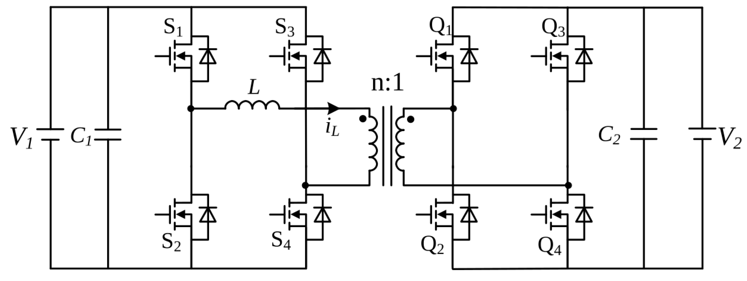

Table 1.
Main parameters of the studied dual-active-bridge converter.
| Value | Symbol | Parameter |
|---|---|---|
| 80-120 V (100 V rated) | Vin | Input voltage |
| 60 V | Vref | Output-voltage reference |
| 10 kHz | fs | Switching frequency |
| 1:1 | n | Transformer turns ratio |
| 50 μH | Llk | Equivalent leakage inductance |
| 470 μF | Co | Output capacitance |
| 10-20 Ω (15 Ω rated) | R | Load resistance |
| 240 W | P | Rated power |
| 0.2 | Kp | PI proportional gain |
| 1 | Ki | PI integral gain |
2.2. Triple-Phase-Shift Modulation
In TPS modulation, D1 and D3 describe the inner phase shifts of the primary and secondary full bridges, respectively, whereas D2 describes the relative phase shift between the bridge voltages. These quantities jointly determine the voltage applied to the equivalent leakage inductance and hence the current trajectory within each switching period [5,6,7].
Figure 2.
Typical triple-phase-shift switching and leakage-inductor-current waveforms.
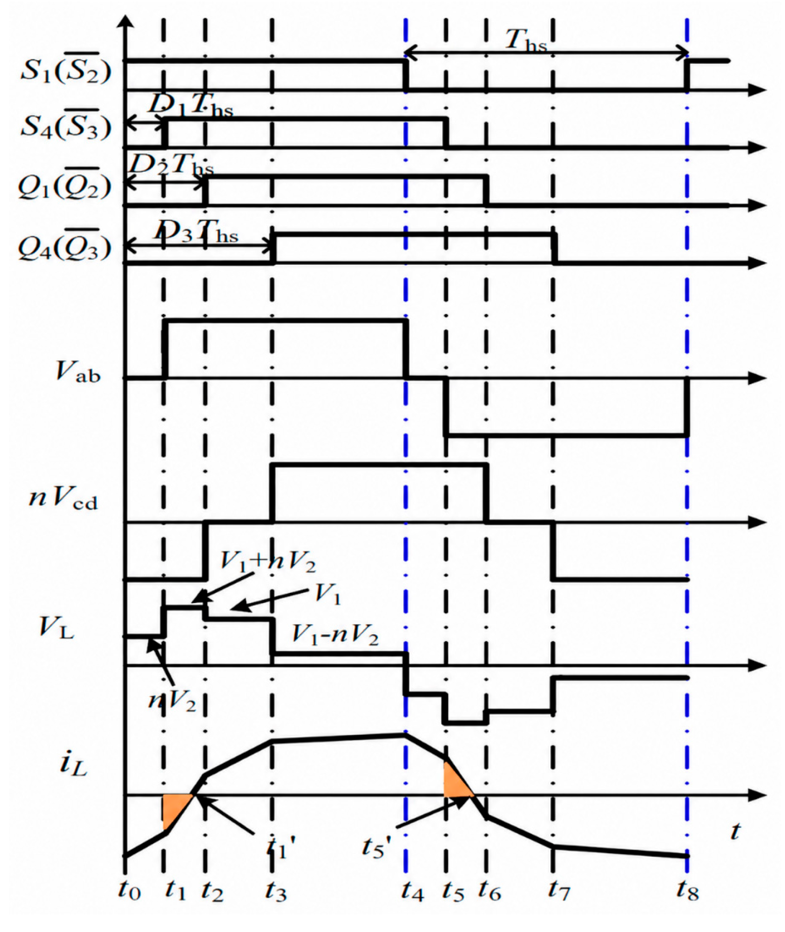
TPS provides greater optimization freedom than single-phase-shift modulation because the transferred power and converter operating condition can be adjusted through three modulation variables. However, the additional variables should not be regarded as three completely independent actuators. The physical effects of , , and partially overlap, and a variation in one variable may change the effective influence of the other two. Therefore, the feasible modulation trajectory is determined by their coordinated values rather than by each variable individually.
This coupling is important when reinforcement learning is introduced into the control loop. A controller that directly modifies all three variables has more local adjustment freedom, but the learning agent must identify the interaction among the modulation variables and avoid action combinations that are ineffective or poorly coordinated. In contrast, a controller that modifies only the high-level phase-shift command operates in a lower-dimensional action space, while the conventional TPS mapping retains responsibility for coordinating , , and . This distinction motivates the comparison between direct compensation of all three TPS variables and compensation of a single high-level phase-shift command.
2.3. Control Structures
Three control structures are considered in this work. The first is the conventional PI-TPS controller, which is used as the baseline. The second introduces RL compensation directly into the three final TPS variables. The third applies RL compensation at the phase-shift-command level before the TPS mapping is executed.
2.3.1. PI-TPS Baseline
The PI-TPS controller is used as the baseline. The output-voltage error is
where Vref is the reference voltage and Vo is the measured output voltage. The PI controller generates the phase-shift command
The TPS controller then maps this high-level command to the three final modulation variables:
This architecture retains a single voltage-regulation command while delegating the internal coordination of D1, D2, and D3 to the TPS mapping.
2.3.2. Direct D1–D2–D3 RL Compensation
In the direct-compensation structure, the PI-TPS controller first generates D1,PI, D2,PI, and D3,PI. The RL agent then provides three additive actions:
The normalized control problem is therefore three-dimensional. This gives the agent direct authority over the final modulation variables, but it also requires the agent to learn their coupled effects. In the implemented agent, each compensation term is bounded within ±0.002.
2.3.3. Phase-Shift-Level RL Compensation
In the phase-shift-level structure, the RL agent does not alter D1, D2, and D3 independently. Instead, it generates one correction to the PI output:
and the TPS controller calculates the final modulation variables as
The action dimension is reduced from three to one, and the TPS mapping remains responsible for coordinating the final modulation variables. The normalized RL action is scaled so that the phase-shift correction remains a small supplementary quantity rather than replacing the PI command.
Figure 3.
Control structures: (a) PI-TPS baseline; (b) direct D1–D2–D3 reinforcement-learning compensation; and (c) phase-shift-level reinforcement-learning compensation.
Figure 3.
Control structures: (a) PI-TPS baseline; (b) direct D1–D2–D3 reinforcement-learning compensation; and (c) phase-shift-level reinforcement-learning compensation.
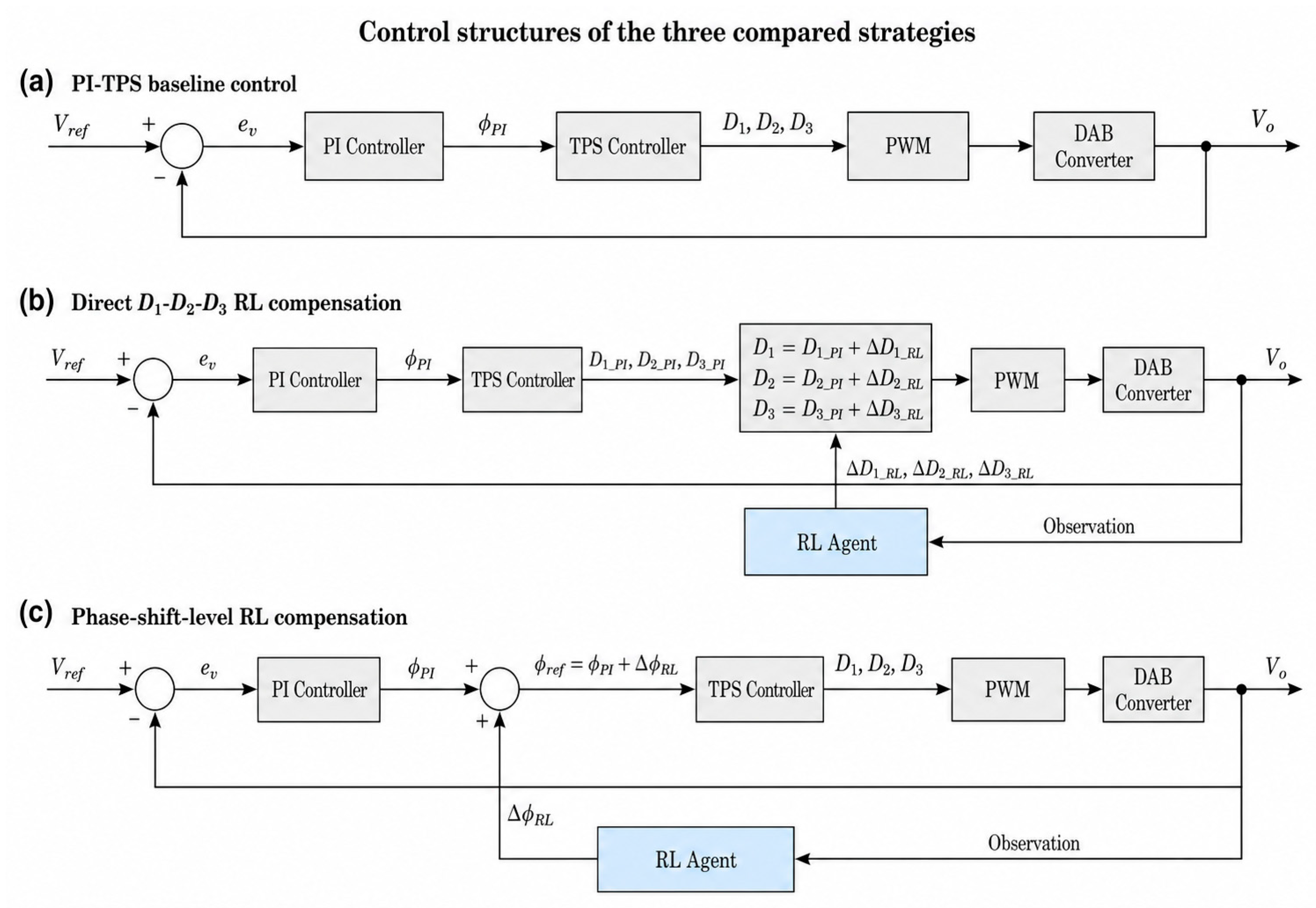
Table 2.
Comparison of the three control strategies.
| Insertion point | Action dimension | RL output | Baseline PI-TPS | Control strategy |
|---|---|---|---|---|
| None | 0 | None | Yes | PI+TPS |
| After TPS mapping | 3 | ΔD1, ΔD2, ΔD3 | Yes | PI+TPS+RL-D123 |
| Before TPS mapping | 1 | Δφ | Yes | PI+TPS+RL-φ |
2.4. Reinforcement Learning Training, Simulation Setup, and Evaluation Indices
2.4.1. Reinforcement Learning and Simulation Settings
Both compensation agents use deep deterministic policy gradient (DDPG), which is suitable for continuous action spaces. The RL-D123 observation vector contains nine quantities: voltage error, output voltage, output current, input voltage, output power, current-stress measure, and the three PI-TPS variables. Its action vector contains three corrections. The RL-φ observation vector contains six quantities: voltage error, output voltage, output current, input voltage, current-stress measure, and the PI-generated phase-shift command; its action is one-dimensional [9].
The agent sample time is 100 μs for both methods, equal to one switching period at 10 kHz. The training episode lengths and optimizer settings differ because the two action spaces and network implementations were tuned separately. The parameters are listed in Table 3.
For the variable-input-voltage study, both RL agents are retrained rather than directly reusing policies trained only at 100 V. The retraining range covers 80–120 V so that the learned policy can respond to changes in the converter voltage ratio while retaining the original PI-TPS baseline. The fixed-point evaluation uses Vin = 80, 90, 100, 110, and 120 V. The voltage-step test uses the sequence 100–80–100–120–100 V with transitions at 0.2, 0.4, 0.6, and 0.8 s. The complementary load evaluation fixes Vin at 100 V and tests R = 10, 12.5, 15, 17.5, and 20 Ω together with the sequence 15–20–15–10–15 Ω.
2.4.2. Evaluation Indices
The steady-state window is selected as 0.18–0.20 s. The steady-state voltage error is calculated from the mean output voltage in this interval:
The steady-state voltage root-mean-square error (RMSE) is
The steady-state voltage ripple is
The full-transient peak inductor current and steady-state RMS inductor current are defined as
To quantify the variation of the final TPS variables, the steady-state control-smoothness index (CSI) is defined as
where ΔDi(k)=Di(k+1)−Di(k). A smaller CSI indicates smaller average point-to-point changes. The maximum vector jump and the standard deviations of D1, D2, and D3 are also reported. These indices distinguish bounded small-amplitude ripple from large control discontinuities.
2.4.3. Multi-Operating-Condition Indices
For the five fixed input-voltage points, the mean and worst-case values of voltage error, voltage RMSE, voltage ripple, current-stress index, RMS inductor current, peak inductor current, efficiency, and CSI are calculated across all operating points. This dual reporting scheme distinguishes average performance from the most demanding condition and allows the consistency of each controller to be assessed over the entire operating range. For the input-voltage step sequence, the peak absolute voltage deviation, 1% and 2% settling times, peak current-stress index, and peak inductor current are evaluated for each transition. The same mean/worst aggregation is used for the five fixed-load points and for the four load transitions. Aggregate indices summarize cross-condition robustness, while the individual points and transitions are retained to avoid masking local deterioration. It also helps identify whether an apparent overall improvement is produced by broad gains or by a few favorable points.
3. Rated-Condition Results and Discussion
3.1. Output-Voltage Regulation
Figure 4.
Output-voltage responses of the three control strategies.
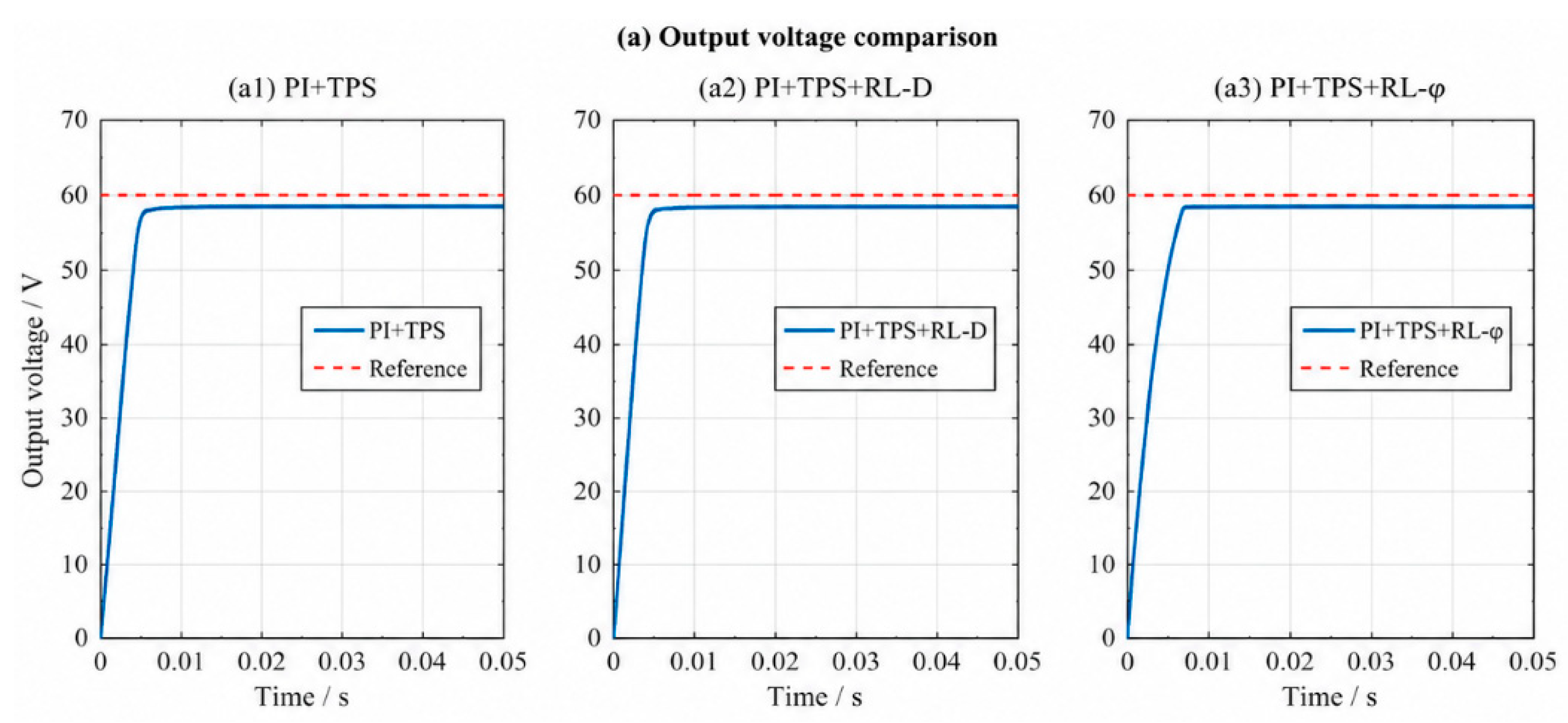
All three strategies regulate the output voltage without overshoot. The PI+TPS baseline reaches a steady-state average voltage of 59.386298 V, corresponding to a voltage error of 0.613702 V. Direct D1-D2-D3 compensation yields 59.386370 V and an error of 0.613630 V. The difference from the baseline is only 72 μV in average voltage, showing that the learned direct actions provide essentially no additional voltage-regulation benefit in the investigated case.
The PI+TPS+RL-φ strategy reaches a steady-state average voltage of 59.566354 V and reduces the voltage error to 0.433646 V, a 29.34% reduction relative to the baseline. Its steady-state RMSE is also reduced from 0.618845 V to 0.440578 V. The improvement is therefore not limited to the final sample; it is maintained over the full steady-state evaluation window. This confirms a persistent improvement rather than a momentary numerical advantage.
The startup trajectories should be interpreted together with the current response. The φ-level strategy enters the 2% tolerance band without overshoot through a more gradual voltage build-up, so the shorter settling time does not imply a more aggressive initial command.
3.2. Current Stress and Dynamic Performance
The steady-state average current-stress index of PI+TPS is 4.548739. The RL-D123 value is 4.549014, a change of only +0.006%, which should be interpreted as practically unchanged rather than as a meaningful deterioration. The RL-φ value is 4.531973, corresponding to a modest 0.369% reduction. Although the steady-state reduction is small, it is achieved together with a clear improvement in voltage accuracy.
Table 4.
Steady-state performance under the rated condition.
| Current-stress change | Voltage-error change | Average current stress | Voltage error / V | Average Vo / V | Control strategy |
|---|---|---|---|---|---|
| — | — | 4.548739 | 0.613702 | 59.386298 | PI+TPS |
| +0.006% | −0.012% | 4.549014 | 0.613630 | 59.386370 | PI+TPS+RL-D123 |
| −0.369% | −29.34% | 4.531973 | 0.433646 | 59.566354 | PI+TPS+RL-φ |
Figure 5.
Current-stress responses of the three control strategies.
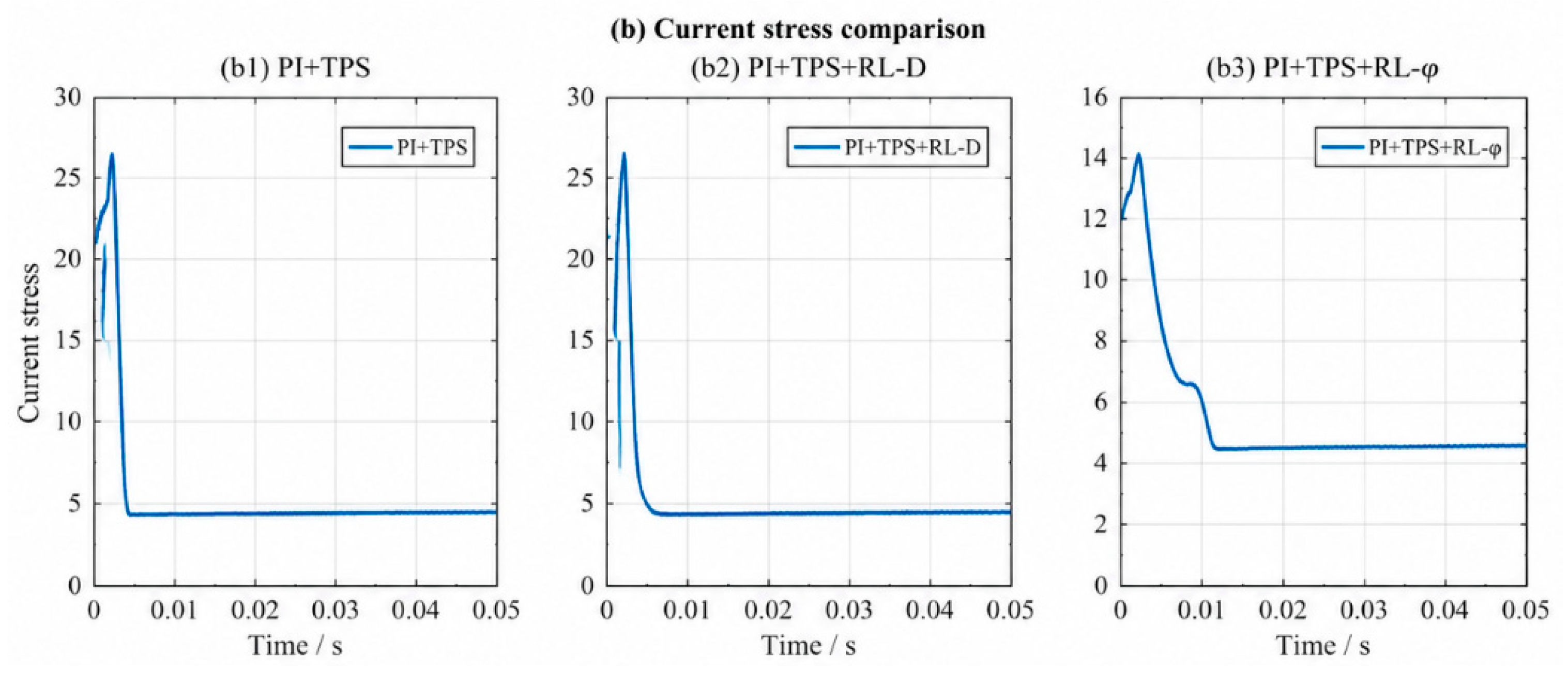
The dynamic indices in Table 5 provide additional information. The 2% settling time of RL-φ is 5.593 ms, compared with 70.986 ms for PI+TPS. Its full-transient peak inductor current is 36.8378 A, approximately 47.24% lower than the baseline value of 69.8237 A. This substantial peak reduction is consistent with the slower, more gradual initial voltage build-up visible in the waveform. Thus, the φ-level strategy does not simply make the response more aggressive; rather, it achieves faster entry into the 2% band while limiting the largest startup-current excursion.
Peak and RMS current describe different operating phenomena: the full-transient peak reflects startup stress, whereas the steady-state RMS value characterizes the conduction burden after regulation has been established. A lower startup peak can therefore coexist with nearly unchanged steady-state RMS current.
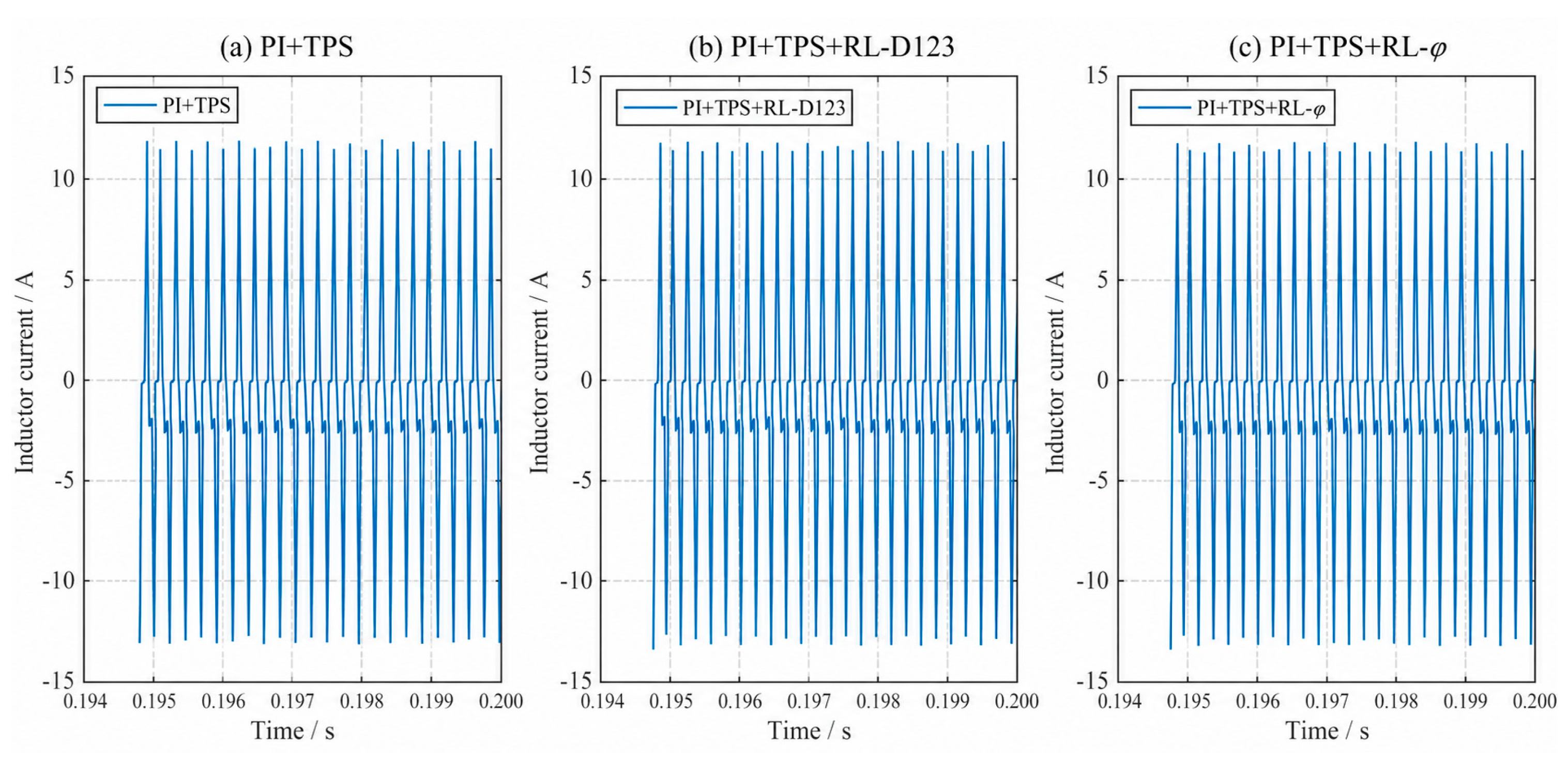
3.3. Steady-State Inductor Current
The three steady-state inductor-current waveforms have similar high-frequency shapes and nearly identical RMS values of approximately 6.132 A. Their steady-state current peaks are 14.278669 A, 14.264871 A, and 14.242303 A for PI+TPS, RL-D123, and RL-φ, respectively. The differences are small, which is consistent with the modest change in the average current-stress index. The main current-related advantage of RL-φ is therefore the reduction of the startup peak rather than a major alteration of the steady-state switching-current waveform.
Figure 6.
Steady-state leakage-inductor-current waveforms over selected switching periods.
3.4. TPS Variables
To examine whether the learned corrections alter the modulation hierarchy, Figure 7 compares D1, D2, and D3 for all three strategies. The traces are separated by method so that startup transitions and steady-state ripple can be inspected without curve overlap.
The direct-compensation agent converges to small nearly constant offsets, with steady-state averages of approximately +5×10⁻⁴, −5×10⁻⁴, and +5×10⁻⁴ for ΔD1, ΔD2, and ΔD3. Consequently, the final TPS variables remain very close to those of the baseline. This observation explains why the voltage and current-stress performance of RL-D123 is almost unchanged.
For RL-φ, the final D1, D2, and D3 trajectories show small bounded periodic variations after the initial transient. These variations should not be described as instability: the variables remain confined around their steady operating values, the output voltage remains regulated, and the quantitative smoothness measures remain comparable to those of the baseline. The periodic component reflects fine discrete-time adjustment of the phase-shift command and the resulting TPS remapping.
3.5. Reinforcement Learning Compensation Outputs
Figure 8 isolates the learned compensation signals themselves. This comparison helps distinguish a genuinely state-dependent corrective policy from a nearly constant bias that produces only a small shift in the final operating point.
The RL-D123 compensation terms are of the order of 10⁻⁴ to 10⁻³ and remain close to constant values during the tested interval. The learned policy therefore behaves mainly as a small static bias correction rather than as a state-dependent dynamic compensation law. This is consistent with the negligible performance difference from PI+TPS.
The phase-shift correction remains close to 10⁻⁴ and exhibits a small bounded oscillation in steady state. Its steady-state average is 9.794274×10⁻⁵, and its maximum steady-state action jump is only 1.492277×10⁻⁷. The plotted vertical scale magnifies these variations; in absolute terms, they are small. The agent therefore provides fine phase-shift regulation without introducing a large disturbance into the baseline loop.
3.6. Control Smoothness
The CSI values are all in the same order of magnitude, and the differences are small. Accordingly, the results do not support a claim of a dramatic smoothness improvement. They do show that the RL compensation layers do not destroy the inherent smoothness of the TPS control variables. RL-D123 is almost indistinguishable from the baseline, whereas RL-φ gives the lowest CSI, the lowest maximum jump, and slightly smaller standard deviations. The reduction in CSI relative to PI+TPS is approximately 0.276%. This result supports the more limited conclusion that the small periodic variations observed in the RL-φ waveforms remain bounded and do not degrade overall modulation smoothness.
Table 6.
Steady-state control-smoothness comparison.
| Std(D3) | Std(D2) | Std(D1) | Maximum control jump | CSI | Control strategy |
|---|---|---|---|---|---|
| 1.5510×10⁻² | 1.0340×10⁻² | 1.5510×10⁻² | 6.6612×10⁻³ | 9.1683×10⁻⁶ | PI+TPS |
| 1.5511×10⁻² | 1.0340×10⁻² | 1.5511×10⁻² | 6.6521×10⁻³ | 9.1689×10⁻⁶ | PI+TPS+RL-D123 |
| 1.5387×10⁻² | 1.0258×10⁻² | 1.5387×10⁻² | 6.6303×10⁻³ | 9.1430×10⁻⁶ | PI+TPS+RL-φ |
3.7. Overall Discussion
The comparison shows that action-space dimension alone is not a measure of control capability. The three-dimensional RL-D123 agent has more direct authority, but the learned actions are small and provide no meaningful improvement in the tested condition. A plausible interpretation is that direct additive modification of strongly coupled TPS variables makes it difficult for the agent to discover a useful policy without additional structure, constraints, or richer operating-condition excitation [5].
The one-dimensional RL-φ structure is more aligned with the hierarchy of the original controller. The agent modifies a high-level command, while the deterministic TPS mapping enforces the relationship among D1, D2, and D3. This reduces the learning dimension and embeds prior physical structure in the control architecture. Under the rated condition considered here, this arrangement improves steady-state voltage accuracy and startup peak current while keeping the final modulation variables bounded [6,7,10].
The rated-condition comparison isolates the influence of the action insertion point, whereas the variable-input-voltage study evaluates cross-condition robustness after retraining. The two agents were trained independently and their optimizer settings were tuned separately; therefore, the results demonstrate a structural trend rather than a universal optimum. Multiple random seeds, identical training budgets, load steps, reference changes, wide-power-range operation, and experimental implementation remain necessary for a complete statistical and hardware-level validation.
4. Variable-Input-Voltage Results
4.1. Test Protocol
The variable-input-voltage evaluation contains two complementary tests. First, each method is operated at fixed input voltages of 80, 90, 100, 110, and 120 V. Each simulation lasts 0.30 s, and the steady-state statistics are calculated over 0.28–0.30 s. Second, the input voltage follows the sequence 100–80–100–120–100 V over a 1.0-s simulation, with each stage lasting 0.20 s. The voltage reference remains 60 V and the load resistance remains 15 Ω. The fixed-point test characterizes operating-range consistency, whereas the step test reveals the dynamic response to abrupt changes in the converter voltage ratio.
4.2. Fixed Input-Voltage Operating Points
Figure 9 compares the fixed-point voltage-regulation and current-related indices. The PI-TPS baseline maintains regulation over the complete 80–120 V range, but its performance varies with the input voltage. Direct D1-D2-D3 compensation does not provide a systematic improvement. Across the five operating points, the mean voltage error increases from 0.7095% to 0.7128%, the mean steady-state voltage RMSE increases from 0.4391 V to 0.4430 V, and the worst voltage ripple increases from 0.5173 V to 0.6336 V. The mean current-stress index also rises from 4.8701 to 5.0050, while the worst current-stress index increases from 6.7469 to 7.0930. The corresponding worst peak inductor current increases from 22.5258 A to 23.9164 A. These results indicate that the additional three-dimensional action authority does not translate into robust cross-condition benefit.
By contrast, the retrained PI+TPS+RL-φ strategy gives the most favorable overall voltage-current tradeoff in the complete variable-voltage comparison. Its mean voltage error is 0.6439%, its worst voltage error is 1.2132%, and its mean steady-state voltage RMSE is 0.4018 V, all lower than the corresponding PI-TPS and RL-D123 values. The worst voltage ripple is reduced to 0.5115 V. Its mean current-stress index is 4.8703, which is practically identical to the PI-TPS value of 4.8701, whereas its worst current-stress index and worst peak inductor current are the lowest at 6.7367 and 22.5188 A, respectively. The mean efficiency is 89.1074%, marginally higher than that of the baseline. Therefore, RL-φ ranks best in seven of the eight aggregate fixed-point indices; only the mean current-stress index is very slightly higher than PI-TPS by approximately 0.0047%. This advantage is not attributed merely to a smaller action dimension. The single learned correction acts on the physically meaningful phase-shift command, after which the deterministic TPS mapping preserves the coordinated relationship among D1, D2, and D3.
Table 7.
Aggregate performance across five fixed input-voltage points.
| PI+TPS+RL-φ | PI+TPS+RL-D123 | PI+TPS | Index |
|---|---|---|---|
| 0.6439 | 0.7128 | 0.7095 | Mean voltage error / % |
| 1.2132 | 1.2857 | 1.2818 | Worst voltage error / % |
| 0.4018 | 0.4430 | 0.4391 | Mean voltage RMSE / V |
| 0.5115 | 0.6336 | 0.5173 | Worst voltage ripple / V |
| 4.8703 | 5.0050 | 4.8701 | Mean current-stress index |
| 6.7367 | 7.0930 | 6.7469 | Worst current-stress index |
| 22.5188 | 23.9164 | 22.5258 | Worst peak iL / A |
| 89.1074 | 88.7134 | 89.0875 | Mean efficiency / % |
All fixed-point indices are calculated over Vin = 80, 90, 100, 110, and 120 V. Lower values indicate better performance except for mean efficiency, for which a higher value is preferable.
4.3. Input-Voltage Step Response
The step sequence exposes the controller to both downward and upward input-voltage changes. Figure 10 presents the stage-wise output-voltage, current-stress, and inductor-current indices for the 100–80–100–120–100 V sequence, while Figure 11 summarizes the four transition metrics. Direct compensation increases the mean peak voltage deviation from 0.8748 V to 0.9355 V and the worst deviation from 1.5694 V to 1.6388 V. The worst 2% settling time increases from 69.385 ms to 78.629 ms. Its worst transition peak inductor current changes only from 27.0343 A to 26.9888 A, a reduction of approximately 0.17%, which is too small to offset the deterioration in voltage regulation. By comparison, RL-φ reduces the mean peak voltage deviation to 0.8673 V and the worst deviation to 1.5390 V. Its mean and worst 2% settling times are 15.421 ms and 61.683 ms, respectively, and its worst transition current stress and worst transition peak inductor current decrease to 10.0165 and 25.3816 A. Thus, RL-φ gives the best value for all six aggregate transition indices.
The phase-shift-level strategy gives the best overall transition behavior in the complete three-method comparison. All six aggregate transition indices are lower than those of PI-TPS and RL-D123. This conclusion refers to the overall multi-transition tradeoff and does not require every local sample-level quantity at every individual transition to be the absolute minimum. Because ΔφRL modifies the common high-level command, the policy can adapt transferred power without directly breaking the internal TPS relationship. This is particularly important during input-voltage steps, when the same independent D1-D2-D3 perturbation can have different effects at different voltage ratios. The variable-voltage results therefore strengthen the rated-condition conclusion: the action insertion point determines whether the learned policy generalizes as a structured correction or behaves as an operating-point-dependent bias.
Table 8.
Aggregate performance for the four input-voltage transitions.
| PI+TPS+RL-φ | PI+TPS+RL-D123 | PI+TPS | Index |
|---|---|---|---|
| 0.8673 | 0.9355 | 0.8748 | Mean peak voltage deviation / V |
| 1.5390 | 1.6388 | 1.5694 | Worst peak voltage deviation / V |
| 15.421 | 19.657 | 17.346 | Mean 2% settling time / ms |
| 61.683 | 78.629 | 69.385 | Worst 2% settling time / ms |
| 10.0165 | 10.6126 | 10.6306 | Worst transition current stress |
| 25.3816 | 26.9888 | 27.0343 | Worst transition peak iL / A |
All transition indices are calculated over the four voltage steps 100→80 V, 80→100 V, 100→120 V, and 120→100 V. Lower values indicate better aggregate transient performance.
4.4. Cross-Condition Interpretation and Method Selection
The combined rated-point and variable-input-voltage results support selection of the third structure for subsequent multi-condition studies. The direct agent has three output channels and nominally greater freedom, but it must learn both power regulation and the coupling constraints among the TPS variables. Its actions can therefore become dependent on the training distribution and may not preserve the intended modulation hierarchy when the voltage ratio changes. The φ-level agent instead learns a compact correction in the same command space used by the PI voltage loop. The TPS mapping acts as an embedded physical prior, converts the single correction into coordinated modulation variables, and limits the extent to which the learned policy can generate physically inconsistent combinations. This comparison therefore evaluates not only nominal performance, but also whether the control architecture preserves coordinated behavior when the operating point moves away from the training-centered condition [10,11].
The load-variation study reported next tests this structural expectation without changing the input-voltage ratio. Reference-voltage changes, bidirectional power transfer, wider load ranges, and experimental implementation remain future extensions. Retaining the third method provides a scalable path because additional operating conditions can be incorporated through observation and training design without expanding the action dimension or removing the deterministic TPS coordination layer [12,13].
5. Load-Variation Results at Fixed 100 V Input
5.1. Test Protocol
To isolate load robustness from the effect of the converter voltage ratio, the input voltage is fixed at 100 V and the output-voltage reference remains 60 V. The fixed-load evaluation uses R = 10, 12.5, 15, 17.5, and 20 Ω. Each operating point is simulated for 0.30 s, and the steady-state statistics are calculated over 0.28–0.30 s. The load-step evaluation uses the sequence 15–20–15–10–15 Ω over 1.0 s, with each load held for 0.20 s and transitions at 0.2, 0.4, 0.6, and 0.8 s. The three control structures are compared using the same voltage-regulation, current-stress, and inductor-current indices defined in Section 2.4. Using identical test durations and evaluation windows ensures that any observed differences arise from the controller structures rather than from unequal numerical treatment.
5.2. Fixed-Load Operating Points
All three strategies maintain stable regulation over the complete 10–20 Ω range, and no phase-shift saturation or problem flag is observed. Figure 12 shows the individual operating-point values, whereas Table 9 reports the corresponding mean and worst-case indices. The following results therefore emphasize both consistency and worst-case robustness.
RL-D123 gives the numerically lowest mean and worst voltage-error percentages, but the advantage is only 0.00214 and 0.00708 percentage points relative to RL-φ. This small voltage-error difference is accompanied by a 22.00% higher worst ripple, an 11.31% higher worst peak current-stress index, and a 12.15% higher worst peak inductor current. RL-φ therefore produces the more favorable fixed-load tradeoff: it gives the lowest mean and worst voltage RMSE, the lowest mean ripple, the lowest mean peak current stress, and the lowest mean peak inductor current, while remaining essentially coincident with the PI-TPS baseline in the other indices.
5.3. Load-Step Response
The 15–20–15–10–15 Ω sequence includes both load release and load increase, with the 15→10 Ω transition representing the largest rise in demanded output current. Figure 13 presents the stage-wise steady-state values, and Figure 14 summarizes the four transition metrics. Across the five stages, RL-φ remains almost identical to PI-TPS in mean voltage error (0.37771% versus 0.37765%), mean current stress (4.69326 versus 4.69322), and mean RMS inductor current (6.29118 versus 6.29132 A). In contrast, RL-D123 increases the mean voltage ripple to 0.38877 V and the mean stage peak inductor current to 16.0012 A, compared with 0.29918 V and 14.1464 A for RL-φ.
Table 10.
Aggregate performance for the four load transitions.
| RL-φ vs. RL-D123 | PI+TPS+RL-φ | PI+TPS+RL-D123 | PI+TPS | Index |
|---|---|---|---|---|
| −4.08% | 0.52876 | 0.55125 | 0.52238 | Mean peak voltage deviation / V |
| −5.97% | 0.64970 | 0.69096 | 0.64977 | Worst peak voltage deviation / V |
| At/below resolution | 0.00000 | 0.00075 | 0.00075 | Mean 2% settling time / ms |
| At/below resolution | 0.00000 | 0.00100 | 0.00100 | Worst 2% settling time / ms |
| −7.71% | 6.1744 | 6.6904 | 6.1415 | Mean transition peak stress |
| −11.51% | 7.1133 | 8.0387 | 7.1133 | Worst transition peak stress |
| −7.60% | 15.1368 | 16.3810 | 14.7198 | Mean transition peak iL / A |
| −12.10% | 16.300 | 18.543 | 16.318 | Worst transition peak iL / A |
All transition indices are calculated over 15→20 Ω, 20→15 Ω, 15→10 Ω, and 10→15 Ω. Lower values indicate better performance. The reported 0-0.001 ms settling values are at or below the numerical sampling resolution and should not be interpreted as physically exact zero settling time.
The PI-TPS baseline gives the lowest mean peak voltage deviation, mean transition current stress, and mean transition peak current. However, RL-φ gives the lowest worst peak voltage deviation and the lowest worst transition peak inductor current, while all four of its reported 2% settling times are at or below the numerical resolution. More importantly, relative to RL-D123, RL-φ reduces the mean and worst peak voltage deviations by 4.08% and 5.97%, the mean and worst transition peak stress by 7.71% and 11.51%, and the mean and worst transition peak inductor current by 7.60% and 12.10%, respectively.
5.4. Cross-Condition Interpretation
The fixed-load and load-step results reinforce the structural conclusion obtained from the variable-input-voltage study. The third method does not need to be the absolute minimum for every individual mean index to be preferable: its main advantage is that it remains close to the stable PI-TPS baseline while consistently avoiding the large ripple and current penalties introduced by direct D1-D2-D3 compensation. The high-level Δφ action preserves the deterministic TPS coordination and therefore behaves as a bounded supplementary correction across both voltage-ratio and load changes. For subsequent multi-condition studies, RL-φ is consequently the most defensible method because it provides the strongest worst-case robustness and the most balanced voltage-current performance without increasing the action dimension.
6. Conclusions
This paper investigated the influence of RL compensation insertion points on the performance of a low-voltage DAB converter with TPS modulation. The comparison between direct modulation-variable compensation and phase-shift-level compensation shows that the location of RL intervention is a critical factor affecting both control effectiveness and generalization capability.
Direct compensation of the three modulation variables provides limited improvement because the RL agent directly modifies strongly coupled control variables, which increases the difficulty of learning a stable compensation policy. In contrast, the proposed phase-shift-level compensation introduces RL assistance above the existing TPS mapping layer, allowing the conventional modulation strategy to preserve the physical relationships among the modulation variables while the RL agent focuses on high-level correction.
The proposed structure achieves improved voltage regulation and reduced current stress under rated operation and multiple operating conditions, including input-voltage variation and load transitions. These results indicate that reducing the action dimension and aligning the RL action with the hierarchical structure of the conventional controller are effective strategies for improving RL-based power converter control.
Therefore, the phase-shift-level compensation structure is selected as the foundation for further studies involving wider operating ranges, reference variations, and experimental validation.
Author Contributions
Conceptualization, C.L. and H.T.; methodology, C.L.; software, C.L.; validation, C.L., R.Y. and Z.Z.; formal analysis, C.L.; investigation, C.L.; data curation, C.L. and R.Y.; writing—original draft preparation, C.L.; writing—review and editing, Z.Z. and H.T.; visualization, C.L. and Z.Z.; supervision, H.T.; project administration, H.T. All authors have read and agreed to the published version of the manuscript.
Funding
This research was funded by the Doctoral Research Initiation Fund of Northeast Electric Power University, grant number BSJXM-11820.
Data Availability Statement
The simulation data, MATLAB/Simulink models, source code, and trained reinforcement-learning agents supporting the findings of this study are available from the corresponding author upon reasonable request.
Conflicts of Interest
The authors declare no conflicts of interest.
References
- De Doncker, R.W.; Divan, D.M.; Kheraluwala, M.H. A three-phase soft-switched high-power-density dc/dc converter for high-power applications. IEEE Trans. Ind. Appl. 1991, 27, 63–73. [Google Scholar] [CrossRef]
- Kheraluwala, M.N.; Gascoigne, R.W.; Divan, D.M.; Baumann, E.D. Performance characterization of a high-power dual-active-bridge dc-to-dc converter. IEEE Trans. Ind. Appl. 1992, 28, 1294–1301. [Google Scholar] [CrossRef]
- Zhao, B.; Song, Q.; Liu, W.; Sun, Y. Overview of dual-active-bridge isolated bidirectional dc-dc converter for high-frequency-link power-conversion systems. IEEE Trans. Power Electron. 2014, 29, 4091–4106. [Google Scholar] [CrossRef]
- Bai, H.; Mi, C. Eliminate reactive power and increase system efficiency of isolated bidirectional dual-active-bridge dc-dc converters using novel dual-phase-shift control. IEEE Trans. Power Electron. 2008, 23, 2905–2914. [Google Scholar] [CrossRef]
- Wen, H.; Xiao, W. Bidirectional dual-active-bridge dc-dc converter with triple-phase-shift control. In Proceedings of the 28th Annual IEEE Applied Power Electronics Conference and Exposition (APEC), Long Beach, CA, USA, 2013; pp. 1972–1978. [Google Scholar] [CrossRef]
- Harrye, Y.A.; Ahmed, K.H.; Adam, G.P.; Aboushady, A.A. Comprehensive steady-state analysis of a bidirectional dual-active-bridge dc/dc converter using triple-phase-shift control. In Proceedings of the 23rd IEEE International Symposium on Industrial Electronics (ISIE), Istanbul, Türkiye, 2014; pp. 437–442. [Google Scholar] [CrossRef]
- Huang, J.; Wang, Y.; Li, Z.; Lei, W. Unified triple-phase-shift control to minimize current stress and achieve full soft-switching of an isolated bidirectional dc-dc converter. IEEE Trans. Ind. Electron. 2016, 63, 4169–4179. [Google Scholar] [CrossRef]
- Shao, S.; Chen, L.; Shan, Z.; Gao, F.; Chen, H.; Sha, D.; Dragičević, T. Modeling and advanced control of dual-active-bridge dc-dc converters: A review. IEEE Trans. Power Electron. 2022, 37, 1524–1547. [Google Scholar] [CrossRef]
- Lillicrap, T.P.; Hunt, J.J.; Pritzel, A.; Heess, N.; Erez, T.; Tassa, Y.; Silver, D.; Wierstra, D. Continuous control with deep reinforcement learning. arXiv 2015, arXiv:1509.02971. [Google Scholar]
- Tang, Y.; Hu, W.; Xiao, J.; Chen, Z.; Huang, Q.; Chen, Z.; Blaabjerg, F. Reinforcement-learning-based efficiency optimization scheme for the DAB dc-dc converter with triple-phase-shift modulation. IEEE Trans. Ind. Electron. 2021, 68, 7350–7361. [Google Scholar] [CrossRef]
- Tang, Y.; Hu, W.; Zhang, B.; Cao, D.; Hou, N.; Li, Y.W.; Chen, Z.; Blaabjerg, F. Deep-reinforcement-learning-aided efficiency-optimized dual-active-bridge converter for distributed generation systems. IEEE Trans. Energy Convers. 2022, 37, 1251–1262. [Google Scholar] [CrossRef]
- You, W.; Yang, G.; Chu, J.; Ju, C. Deep-reinforcement-learning-based proportional–integral control for a dual-active-bridge converter. Neural Comput. Appl. 2023, 35, 17953–17966. [Google Scholar] [CrossRef]
- Tang, Y.; Hu, W.; Cao, D.; Hou, N.; Li, Z.; Li, Y.W.; Chen, Z.; Blaabjerg, F. Deep-reinforcement-learning-aided variable-frequency triple-phase-shift control for a dual-active-bridge converter. IEEE Trans. Ind. Electron. 2023, 70, 10506–10515. [Google Scholar] [CrossRef]
Figure 7.
D1, D2, and D3 under the three control strategies. Each variable is presented using three vertically separated traces to avoid overlap.
Figure 7.
D1, D2, and D3 under the three control strategies. Each variable is presented using three vertically separated traces to avoid overlap.
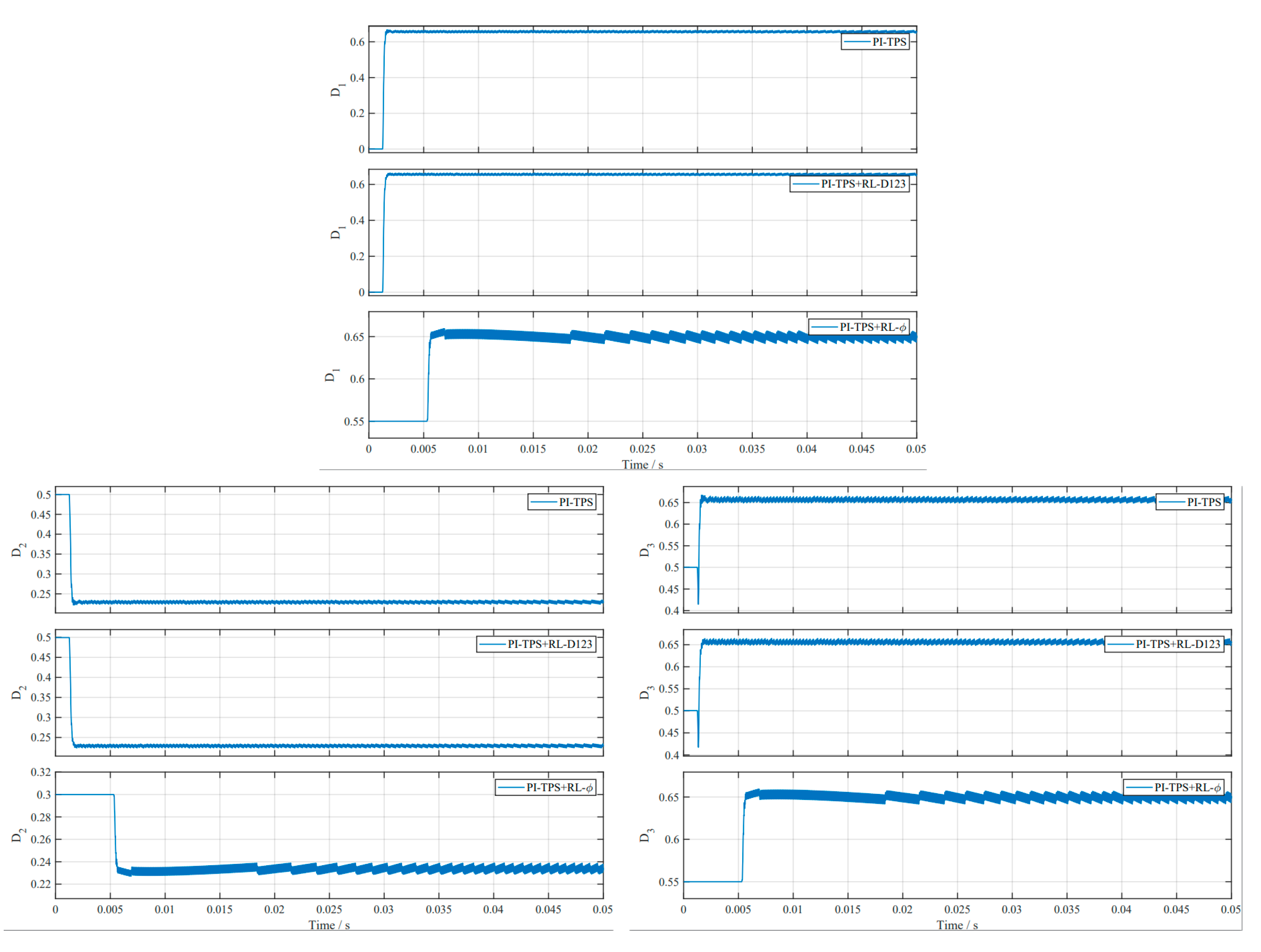
Figure 8.
Reinforcement-learning compensation outputs: ΔD1, ΔD2, and ΔD3; and ΔφRL.
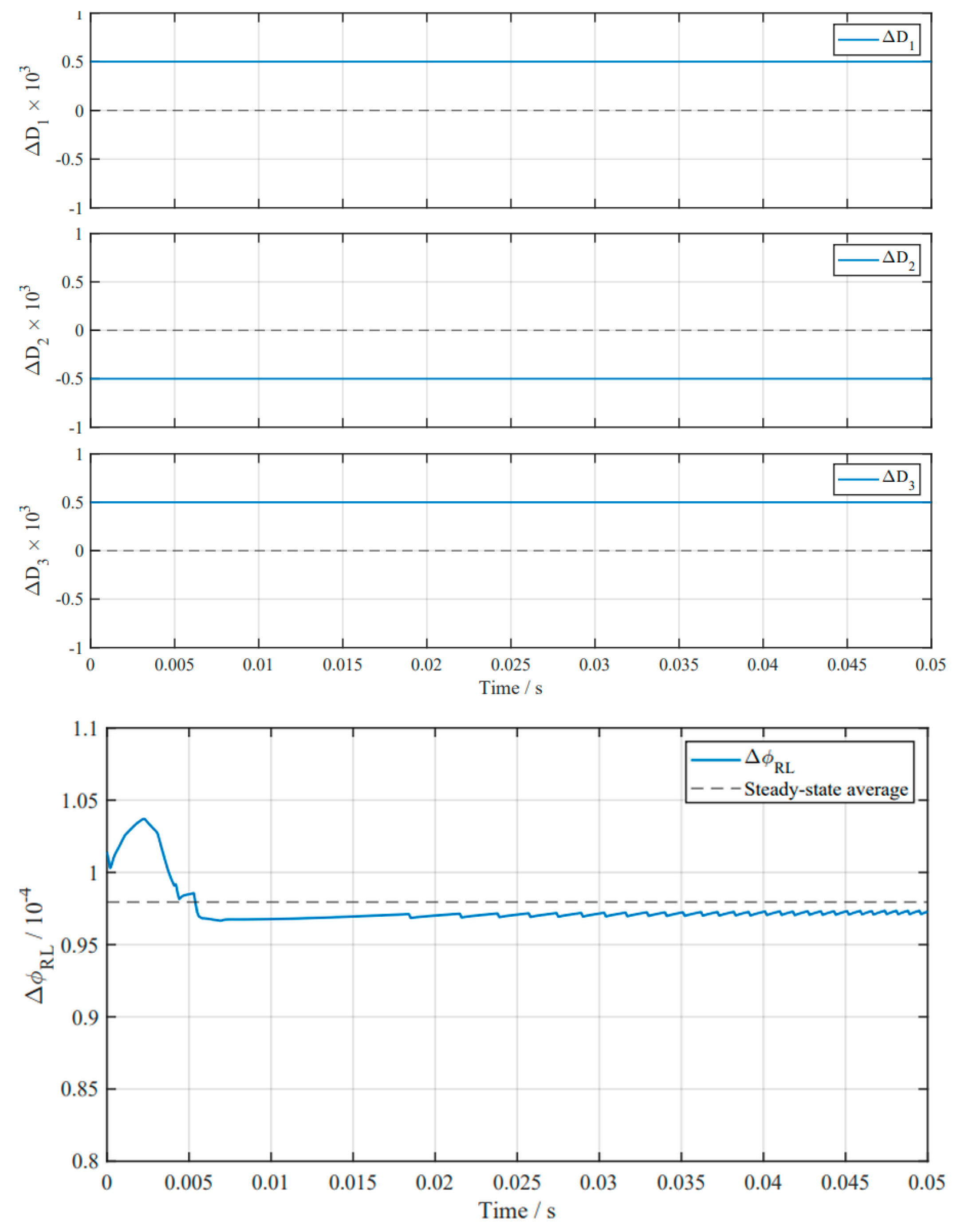
Figure 9.
Fixed-input-voltage performance of the three control strategies over Vin = 80–120 V: output-voltage regulation, voltage error, current stress, and inductor-current indices.
Figure 9.
Fixed-input-voltage performance of the three control strategies over Vin = 80–120 V: output-voltage regulation, voltage error, current stress, and inductor-current indices.
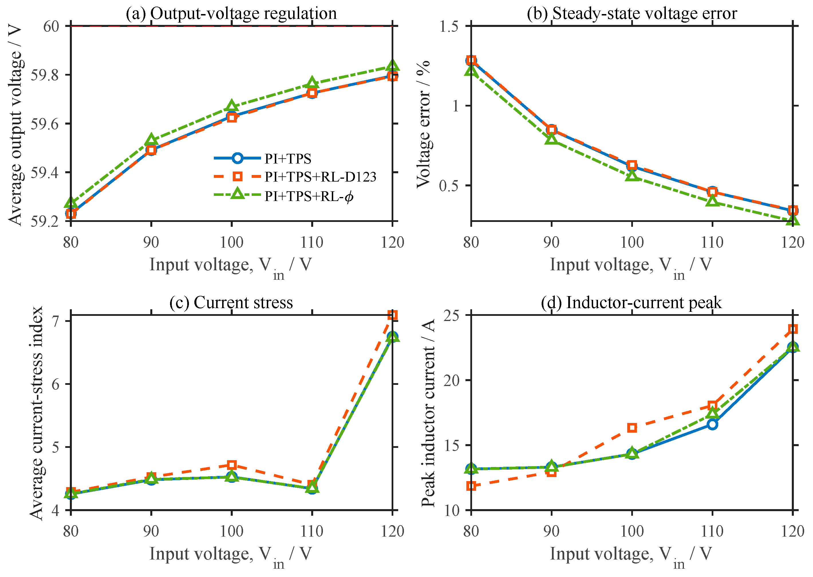
Figure 10.
Stage-wise output-voltage, current-stress, and peak-inductor-current indices under the 100–80–100–120–100 V input-voltage sequence.
Figure 10.
Stage-wise output-voltage, current-stress, and peak-inductor-current indices under the 100–80–100–120–100 V input-voltage sequence.
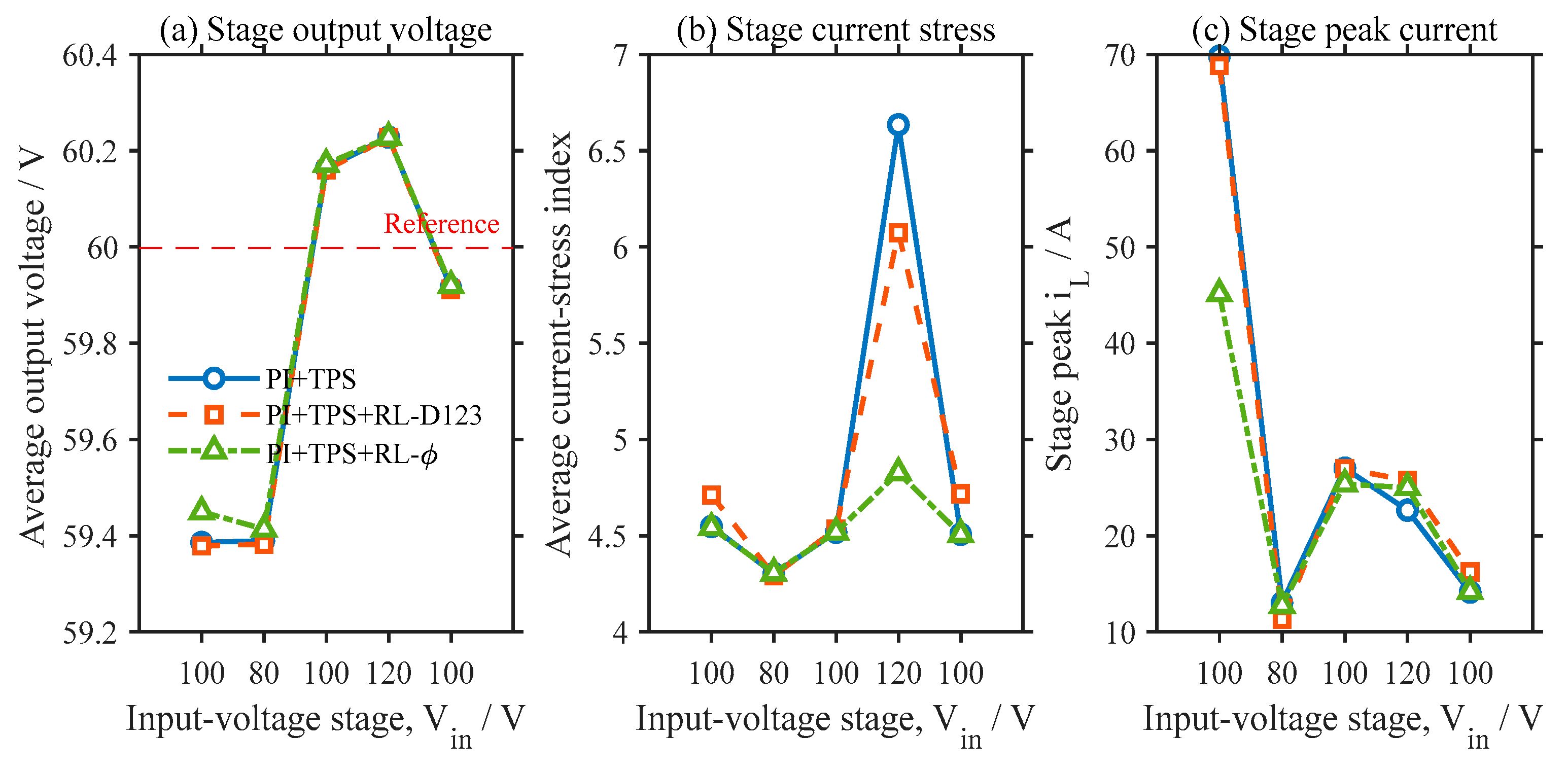
Figure 11.
Transition metrics for the four input-voltage steps: peak voltage deviation, 2% settling time, and peak inductor current.
Figure 11.
Transition metrics for the four input-voltage steps: peak voltage deviation, 2% settling time, and peak inductor current.
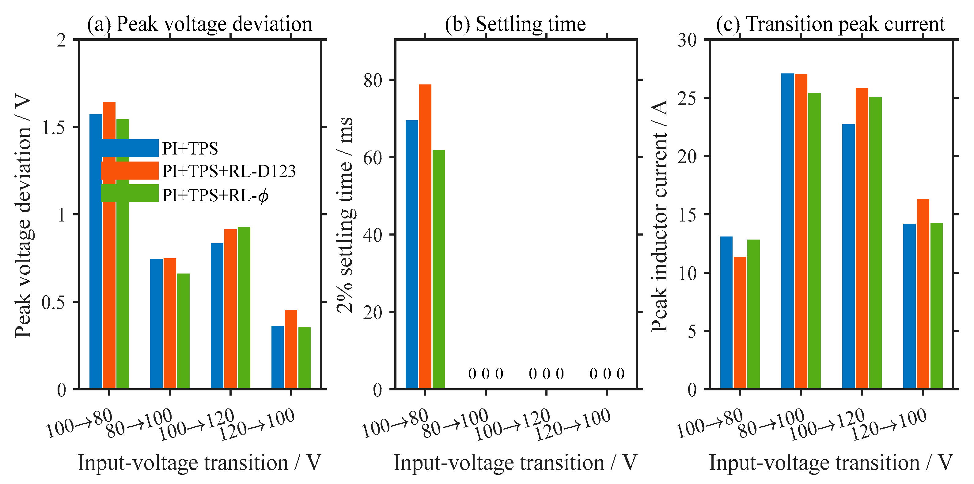
Figure 12.
Fixed-input-voltage performance of the three control strategies over R = 10–20 Ω: output-voltage regulation, voltage error, current stress, and inductor-current indices.
Figure 12.
Fixed-input-voltage performance of the three control strategies over R = 10–20 Ω: output-voltage regulation, voltage error, current stress, and inductor-current indices.
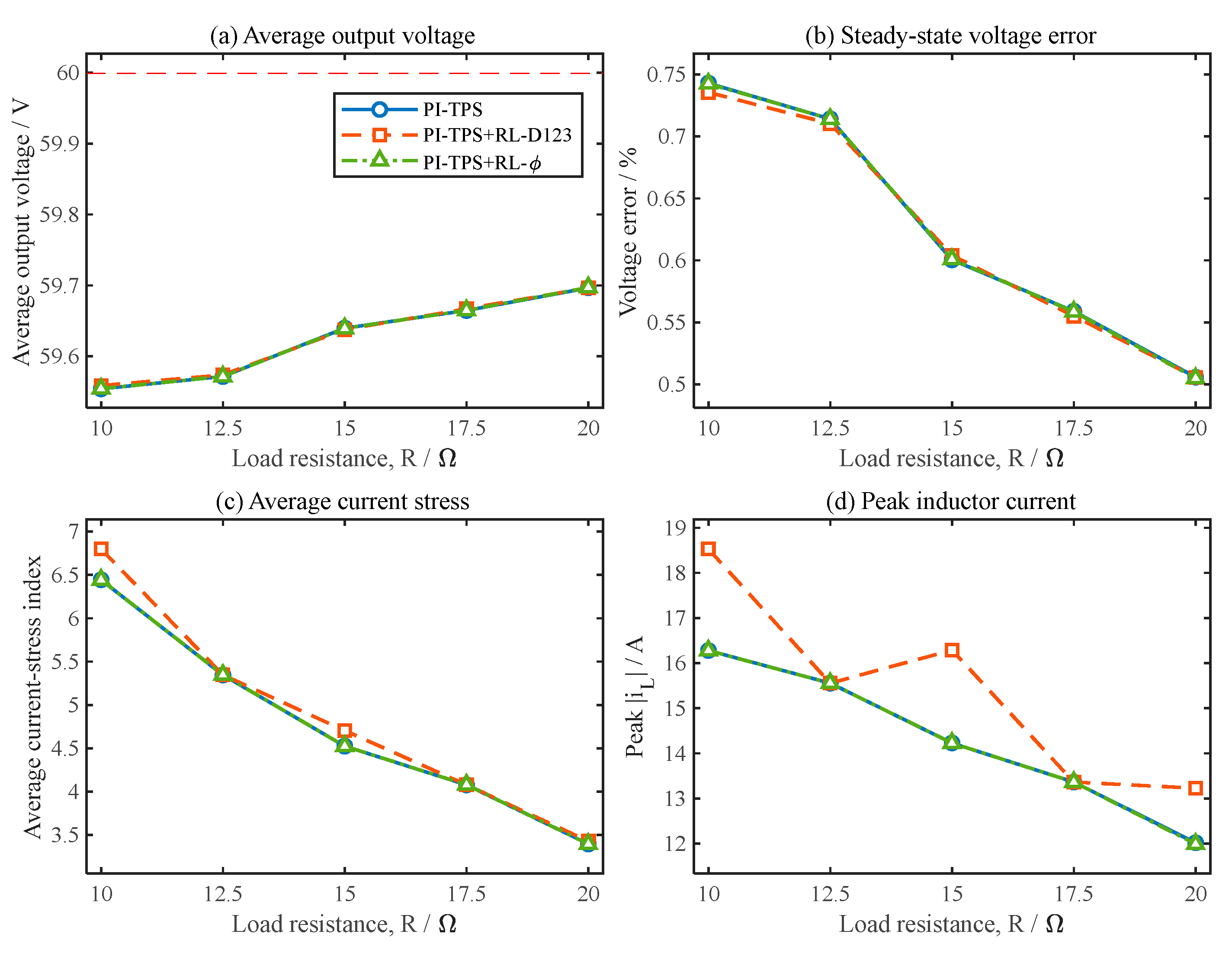
Figure 13.
Stage-wise output-voltage, current-stress, and peak-inductor-current indices under the 15–20–15–10–15 Ω load sequence at Vin = 100 V.
Figure 13.
Stage-wise output-voltage, current-stress, and peak-inductor-current indices under the 15–20–15–10–15 Ω load sequence at Vin = 100 V.
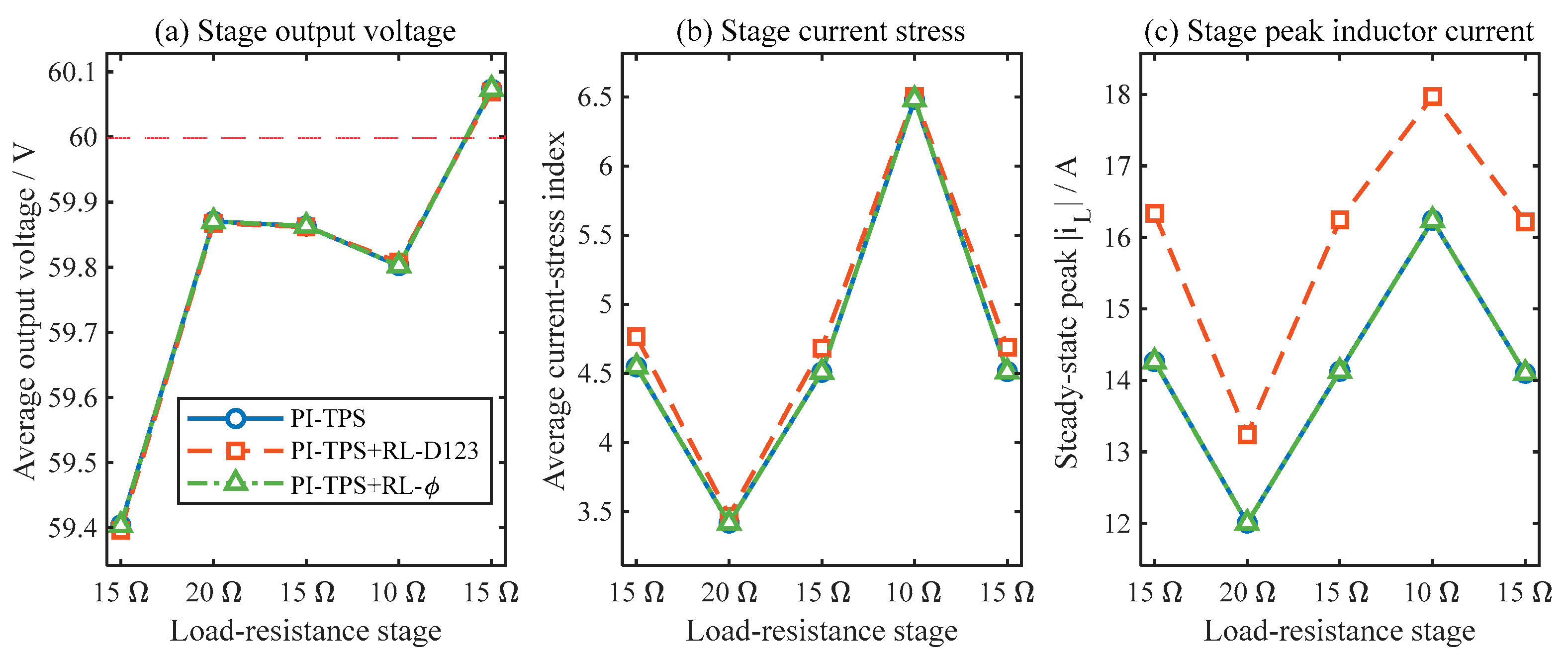
Figure 14.
Transition metrics for the four load steps: peak voltage deviation, 2% settling time, peak current stress, and peak inductor current.
Figure 14.
Transition metrics for the four load steps: peak voltage deviation, 2% settling time, peak current stress, and peak inductor current.
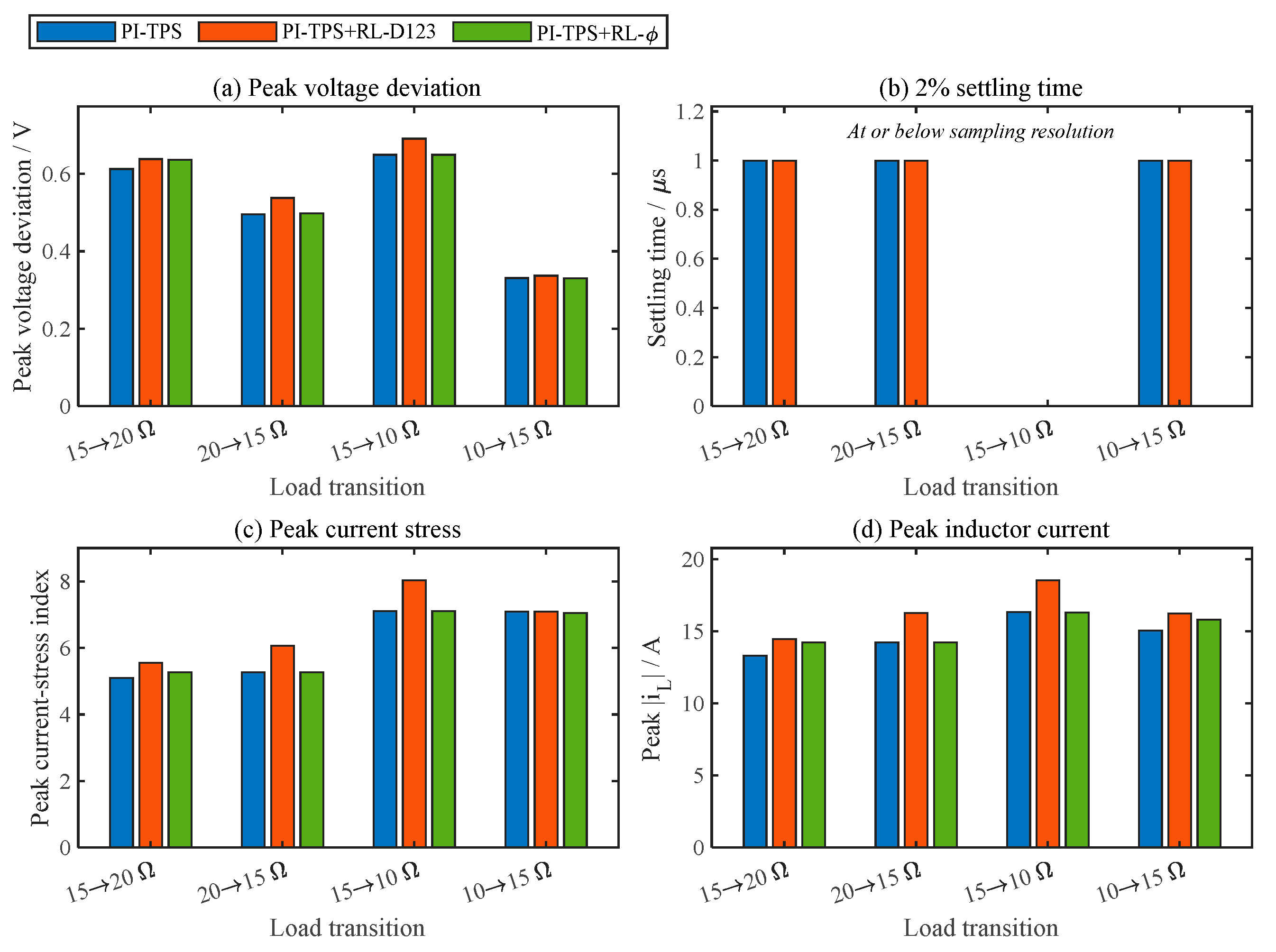
Table 3.
Reinforcement-learning training and simulation parameters.
| RL-φ | RL-D123 | Parameter |
|---|---|---|
| DDPG | DDPG | RL algorithm |
| 6 | 9 | Observation dimension |
| 1 | 3 | Action dimension |
| 1×10⁻⁴ s | 1×10⁻⁴ s | Agent sample time |
| 0.02 s | 0.02 s | Episode simulation time |
| 200 | 200 | Maximum steps per episode |
| 400 | 400 | Maximum training episodes |
| 64 | 64 | Mini-batch size |
| 0.99 | 0.99 | Discount factor |
| 1×10⁵ | 1×10⁵ | Experience buffer length |
| 1×10⁻³ | 1×10⁻³ | Target smooth factor |
| 1×10⁻⁴ | 1×10⁻⁴ | Actor learning rate |
| 2×10⁻⁴ | 2×10⁻4 | Critic learning rate |
| 128 | 128 | Hidden-layer units |
| 1 | 1 | Gradient threshold |
The two agents were trained independently; therefore, their optimizer and episode settings are reported separately rather than interpreted as controlled experimental variables.
Table 5.
Dynamic and current-related performance indices.
| Voltage ripple / V | Steady-state RMS iL / A | Full-transient peak iL / A | Steady-state voltage RMSE / V | Overshoot / % | Settling time / s | Control strategy |
|---|---|---|---|---|---|---|
| 0.349123 | 6.132480 | 69.823748 | 0.618845 | 0 | 0.070986 | PI+TPS |
| 0.344364 | 6.132612 | 68.861517 | 0.618754 | 0 | 0.072786 | PI+TPS+RL-D123 |
| 0.333514 | 6.132014 | 36.837786 | 0.440578 | 0 | 0.005593 | PI+TPS+RL-φ |
Peak current is evaluated over the complete 0–0.20 s simulation. Voltage RMSE, RMS current, and voltage ripple are evaluated over 0.18–0.20 s.
Table 9.
Aggregate performance across five fixed loads at Vin = 100 V.
| RL-φ vs. RL-D123 | PI+TPS+RL-φ | PI+TPS+RL-D123 | PI+TPS | Index |
|---|---|---|---|---|
| +0.34% | 0.62423 | 0.62209 | 0.62445 | Mean voltage error / % |
| +0.96% | 0.74257 | 0.73549 | 0.74294 | Worst voltage error / % |
| −0.02% | 0.38266 | 0.38275 | 0.38279 | Mean voltage RMSE / V |
| −0.03% | 0.45502 | 0.45516 | 0.45524 | Worst voltage RMSE / V |
| −16.17% | 0.31648 | 0.37755 | 0.31687 | Mean voltage ripple / V |
| −22.00% | 0.36545 | 0.46853 | 0.36545 | Worst voltage ripple / V |
| −2.33% | 4.75820 | 4.87160 | 4.75806 | Mean current-stress index |
| −5.23% | 6.44390 | 6.79960 | 6.44360 | Worst current-stress index |
| −7.39% | 5.44060 | 5.87444 | 5.44188 | Mean peak current stress |
| −11.31% | 7.09850 | 8.00350 | 7.09850 | Worst peak current stress |
| −1.42% | 6.33970 | 6.43080 | 6.33948 | Mean RMS iL / A |
| −3.72% | 8.14590 | 8.46080 | 8.14610 | Worst RMS iL / A |
| −7.21% | 14.2838 | 15.3938 | 14.2892 | Mean peak iL / A |
| −12.15% | 16.280 | 18.531 | 16.280 | Worst peak iL / A |
All fixed-load indices are calculated over R = 10, 12.5, 15, 17.5, and 20 Ω. Lower values indicate better performance. The last column gives the relative change of RL-φ with respect to RL-D123; a negative value denotes a reduction.
Disclaimer/Publisher’s Note: The statements, opinions and data contained in all publications are solely those of the individual author(s) and contributor(s) and not of MDPI and/or the editor(s). MDPI and/or the editor(s) disclaim responsibility for any injury to people or property resulting from any ideas, methods, instructions or products referred to in the content. |
© 2026 by the authors. Licensee MDPI, Basel, Switzerland. This article is an open access article distributed under the terms and conditions of the Creative Commons Attribution (CC BY) license (http://creativecommons.org/licenses/by/4.0/).
Copyright: This open access article is published under a Creative Commons CC BY 4.0 license, which permit the free download, distribution, and reuse, provided that the author and preprint are cited in any reuse.


