

Submitted:
29 July 2026
Posted:
30 July 2026
You are already at the latest version
Abstract
Organic Electrochemical Transistors (OECTs) have emerged as continuous monitoring sensors for in-vitro models. Source and Measure Units (SMUs) are typical instruments used to simultaneously control input and output signals on OECTs. Conventional SMUs are unsuitable for in-vitro application due to their limited channels count, large footprint and high cost. This work presents the design and the development of a multichannel, portable and cost-effective SMU platform for the continuous and long-term characterization of OECT biosensors. The hardware is based on an electronic board interfacing via customized connection to a six-OECT set-up, integrated in a standard culture plate and operated within a cell incubator. System functionality is managed by Arduino Nano microcontroller through ad-hoc software, enabling automated characterization of the OECTs. The platform characterization performance is evaluated by comparing the I – V characteristics and transient responses of the tested OECTs with those obtained by the commercial Keysight B2912A SMU. Long-term and continuous operation is verified by a 30 minutes-sampling, five days measurement. The assessed features of the platform and the achieved results suggest that the proposed prototype is more appropriate than conventional SMUs for OECT-based in-vitro biosensing. The presented solution has the potential to support biological research by offering an operator-independent and in-vitro compatible apparatus.
Keywords:
Source and Measure Unit (SMU)
; Organic Electrochemical Transistor (OECT)
; in-vitro platform
; continuous monitoring
; Arduino prototyping
1. Introduction
In the field of biosensing technologies, a novel category of biosensors is represented by Organic Electrochemical Transistors (OECTs). These devices are based on gate, drain and source electrodes and an ion-permeable organic semiconducting (OSC) channel [1]. OECTs operate in contact to an electrolyte, and gate-source voltage variations (input) modulate the drain-source current (output) through ions injection into the channel [2]. To date, OECTs have been exploited for detecting a wide range of analytes, including enzymes, metabolites, antibodies and nucleic acids [3]. Thanks to OSC properties, they have also emerged for biological models monitoring. Indeed, the most common channel material, namely poly3,4-ethylenedioxythiophene-polystyrene-sulfonate (PEDOT:PSS), exhibits electrochemical stability, biocompatibility and enables low voltages operation (< 1 V), endowing OECTs with a relatively high signal amplification [1,2,4].
OECTs are typically characterized by commercial Source and Measure Units (SMUs), instruments which simultaneously provide and measure voltage and current on the same channel [5]. In OECT biosensors characterization, generally the drain-source current (Ids) is measured while supplying a variable gate-source voltage (Vgs) and a constant drain-source voltage (Vds). Through this approach, biochemical processes are examined by the obtained transfer characteristic and transient response [6]. Common SMUs used in research are the B2900 Series by Keysight Technologies and the 2400 Standard Series by Keithley Instruments [7,8,9]. As representative model, the Keysight B2912A features full 4-quadrant operation, a maximum range of ± 210 V / ± 3 A, a maximum resolution of 100 nV / 10 fA, a noise below 100 nV / 10 fA, a maximum sampling rate of 10 μs and a memory buffer of 100,000 data points. It allows the user to configure versatile triggers, current and voltage ranges, and generate customized waveforms through GUI SW and SCPI programming. It supports USB, LAN and GPIB communication with PC and triaxial wiring via BNC connectors [10]. Even though commercial SMUs are state-of-the-art equipment, they are not intended for in-vitro experimentation. Standard models provide only 1 or 2 channels, which are insufficient for biological replicates. Modular and high-density channel models are significantly more expensive [11,12], constituting a considerable barrier for research institutions. Another constraint is the bulkiness, which complicates transportation and set-up in biological laboratories [7,13]. Concerning SW aspects, the limited memory of standard models is inadequate for long-term measurements, thus necessitating a PC for data logging [10,14]. The specialized syntax of the SCPI (Standard Commands for Programmable Instruments) language [15] requires a dedicated study for proper coding.
Hence, there is a need for a compact, affordable and user-friendly SMU that is compatible with in-vitro biosensing. Many low-cost prototypes, although not specifically designed for biosensors, have been developed [7,8,16,17,18]. They are based on Arduino microcontroller units (MCUs), digital-to-analog converters (DACs), analog-to-digital converters (ADCs) and additional HW and SW resources for communication and data management. With regard to biosensing, three recently proposed prototypes are noteworthy. The first, fabricated by Galanti and coworkers [9], integrates a commercial power supply, a general-purpose CPU and an analog circuit for the characterization of graphene field-effect transistors (FETs). It features full 4-quadrants operation, a high signal-to-noise ratio (SNR) and is provided with an electromagnetic interference (EMI) shielding box. The second, constructed by Bryantono et al. [19], is a STM32F1-based circuitry for the I – V tracing of FET biosensors. It presents an optimized architecture to minimize parasitic elements, an enclosing box for heat dissipation and a LabVIEW GUI for data analysis. The third, carried out by Park and colleagues [13], is a WeMos D1-controlled web-based system for measuring the transcharacteristic of ionic liquid-gated FETs. It is capable of automatically storing real-time measurements in a cloud server via wireless communication, generating large datasets for long-term experiments. Despite the achievements, these three systems lack a biosensor integration setup (thereby necessitating external probes), support only single device testing, are limited to I – V characterization (no transient or temporal measurements are reported) and require further HW resources for data analysis.
Based on the aforementioned limitations, in this work we have developed a multichannel, low-cost SMU platform for the I – V and transient response characterization of OECT biosensors. The platform controls a six-OECT set-up integrated in a standard culture plate, housed in a cell incubator during operation. The sensorized plate communicates with the breadboard via flat cables and re-attachable connectors, supporting in-vitro operations. The circuitry is based on Arduino Nano MCU and easy-to-use components, enabling automatic measurement and data logging. The platform features a maximum resolution of 1.22 mV / 78 nA (adequate for OECTs), a maximum per-channel current of ≈ 10 mA (≈ Ids,max) and a low power consumption (≈ 1 W), essential for long-term experiments. The breadboard-based circuitry facilitates prototyping and introduces an acceptable offset (≈ 30 µA) and negligible noise (≈ 150 nA) for this application. The user-friendly Arduino IDE is used for programs development and uploading to the MCU. This operator and PC-independent system is capable to continuously monitor the six OECT biosensors for long-term periods, achieving a large dataset. In this paper, we present the developed SMU platform and validate its OECT characterization performance through comparative measurements executed with the Keysight B2912A SMU. Results demonstrate that this prototype represents a valid alternative to standard SMUs in the context of OECT biosensors characterization. We believe that the proposed solution can support biological research by providing a portable, cost-effective and in-vitro compatible biosensing platform.
2. Materials and Methods
2.1. Hardware Design
2.1.1. SMU Circuit
The proposed SMU circuit, whose block diagram is shown in Figure 1, comprises five functional subsystems: digital, voltage-driving, voltage-sensing, current-sensing and power supply. The digital subsystem includes an MCU, a real-time clock (RTC) for timestamping, a memory card for data and timestamp storage, a red light-emitting diode (LED) for acquisition phase signalling and two multiplexers (MUXs) for converters selection. The MCU communicates with the RTC and MUXs via Inter-Integrated Circuit (I2C) and with the memory card via Serial Peripheral Interface (SPI) protocols. Although not essential for operations, a PC can be connected to the MCU through USB for real-time check. The voltage-driving subsystem consists of six DACs, three generating the gate voltages (Vg) and three the source voltages (Vs) for the OECTs. These voltages feed six operation amplifiers (op-amps) configured as voltage followers (VFs), three driving the Vg and three the Vs signals respectively. VFs source the required currents to the six OECTs while maintaining stable and load-independent driving voltages. OECTs drain voltages (Vd) are fixed to GND (0V). The voltage-sensing subsystem is composed of two ADCs which measure the three gate-source voltages (Vgs) and the 5V power supply, as explained below. The current-sensing subsystem is based on six high-side shunt resistors (Rs) in series with the corresponding OECTs, six instrumentation amplifiers (INAs) and three ADCs. OECTs drain-source currents (Ids) are acquired with the shunt-resistance method: Ids, driven by Vds and flowing on Rs, produces by Ohm’s law a proportional voltage drop (VRs = Ids ∙ Rs), which is amplified by the INA (Vout = GINA ∙ VRs, where GINA is the INA gain) and measured by the ADC. Ids is computed as: Ids = - Vout / (GINA ∙ Rs) (1). The power supply subsystem includes a power supply unit (PSU), providing common GND, single + 8V and bipolar ± 8V lines, a voltage regulator (VR) generating single 5V supply (5VVR), and the low-dropout regulator (LDO) integrated in the MCU, providing single 5V supply (5VMCU). The MCU and VR are powered with + 8V, the op-amps with ± 8V, the converters with 5VVR, and the digital subsystem with 5VMCU. The two 5V sources are used to distribute the power load and prevent interference between the analog and digital circuits. These supply sources are respectively inspected by the MCU and the voltage-sensing ADC to detect eventual power anomalies.
The following sections describe the circuit components and the subsystems schematics, designed with KiCad (v9.0.5). Recurring components are omitted to avoid redundancy.
2.1.2. Digital Subsystem
The digital subsystem (Figure 2) implements Arduino Nano (Arduino) as MCU, which is a compact, low-power and user-friendly development board based on ATmega328 microcontroller (Microchip Technology) [20]. The other devices are based on breakout boards (hereafter referred to as modules), which are modular printed circuit boards (PCBs) containing the core integrated circuit (IC) and auxiliary components such as pull-up resistors, bypass capacitors and LEDs. Breakout boards allow ICs to be easily managed through their breadboard-friendly pins [21]. The RTC consists in the DS3231 module (Maxim Integrated, Adafruit Industries), a battery-integrated and highly accurate clock able to maintain date and time information for long periods [22]. MUXs are based on the TCA9548A module (Texas Instruments, Adafruit Industries), a low-standby current I2C switch able to select among up to eight devices [23]. The high-speed 8 GB USD500S microSDHC (Transcend) is used as memory card, integrated in the microSD card adapter module (Adafruit Industries).
2.1.3. Voltage-Driving Subsystem
The voltage-driving subsystem (Figure 3) exploits as DACs the rail-to-rail, low-power 12-bit MCP4725 modules (Microchip Technology, Adafruit Industries) [24]. The I2C pins of each module are connected to the corresponding I2C channel pins of the DAC-selecting MUX. The modules output signal is processed by a low-pass RC filter, constituted by a 1 KΩ resistor (CFR25 type) and the parallel of a 1 µF ceramic and a 100 nF film capacitors. This two-capacitors filter, with a cutoff frequency of ≈ 145 Hz, attenuates a broad range of noise frequencies while preserving the working signals. VFs are implemented with the LM358 IC (Texas Instruments), which is a cost-effective, low-offset and unity-gain stable dual op-amp [25].
2.1.4. Voltage and Current-Sensing Subsystems
The ADCs of the sensing subsystem (Figure 4) are based on the 4-channel, low-power 16-bit ADS1115 module (Texas Instruments, DFRobot), configured in differential mode for common noise reduction. By incorporating a low-drift voltage reference and a programmable gain amplifier (PGA), ADS1115 supports six input full-scale ranges (FSR) from ± 0.256 V to ± 6.144 V, with corresponding resolutions from 7.812 to 187.5 µV. It offers eight programmable data rate settings, from 8 samples per second (SPS) up to 860 SPS, clocked by an integrated oscillator [26]. The I2C pins are connected to the corresponding I2C channel pins of the ADC-selecting MUX. Shunt resistances consist in a precision 1 Ω resistor (E96 series), whose ends are connected to the positive and negative input pins of the INA121 instrumentation amplifier (Texas Instruments). This high-accuracy INA exhibits high common-mode rejection, low voltage offset and drift, and low bias and quiescent currents. By placing an external resistor RG of 511 Ω (E96 series) between its two Rg pins, the INA gain (GINA = Vout / (Vin+ - Vin-)) was set to approximately 100, according to: GINA = 1 + 50 kΩ / RG [27]. Vout is subsequently processed by a low-pass filter identical to the voltage-driving subsystem one.
2.1.5. Power Supply Subsystem
The series connection of two PeakTech 6080A linear-regulated power supplies (PeakTech) is exploited as bipolar PSU, as shown in the subsystem schematic of Figure 5. A capacitor-input filter placed on the ± 8V lines, constituted by the parallel of a 100 nF film and a 10 µF tantalum capacitors, suppresses high-frequency noise on the power rail. The LM317 VR (Texas Instruments) is downstream of the PSU to generate 5VVR from +8V. This adjustable three-pin regulator supplies an output voltage equal to: Vout = Vref ∙ (1 + Radj / Rref) + Iadj ∙ Radj, where Vref = 1.25 V, Iadj ≈ 50 µA, Rref set to 220 Ω [28] and Radj set to 660 Ω to obtain Vout = 5V. The PSU output was set to 8V to guarantee a minimum headroom of 3 V on the VR, and a 1 KΩ load resistor was placed at VO pin to achieve a minimum output current of 5 mA [29]. Moreover, LM317 is supported by the following external circuitry: a 100 nF bypass film capacitor at VI pin (input voltage stability), a 10 µF tantalum capacitor at ADJ pin (ripple rejection improvement), a 1 µF ceramic capacitor at VO pin (transient response improvement), and two protective 14001G diodes respectively between VO-VI pins and ADJ-VO pins (prevention of capacitors discharging across Vout).
2.1.6. OECT and Wiring Set-Up
The OECT set-up (Figure 6) was customized for integration in a 12-wells culture plate and interfacing with the breadboard. A 25 µm-thick flexible Kapton substrate (DuPont) was selected to allow sensors bending in the wells. Gold was employed for OECT electrodes, interconnections and contact pads, while PEDOT:PSS for the channel [30]. It was designed with a length of 200 µm and a width of 4 mm, while the gate as a 5 x 5 mm gold electrode. A polydimethylsiloxane (PDMS) layer was used for gold passivation. All materials were chosen for their biocompatibility and reliable operation in a biological environment. Following the approach of Fallager et al. [31], a guide-patterned PDMS mold was exploited as interconnector between pads and the stripped wires of a 10 cm-long ribbon cable. Silver paste was used to bond pads and wires, encapsulated by epoxy resin for protection towards the cell incubator humidity (95 % RH). This interconnection block was conceived to prevent short circuits between the bonded contacts and provide them mechanical stability. All aforementioned structures were designed by Rhinoceros CAD software (Robert McNeel). A wiring set-up was engineered for signal transmission between the OECT set-up and the breadboard, consisting of insulation-displacement contact (IDC) connectors linked by a 1 m-long ribbon cable (refer to Figure 9). Ferrite rings, enclosing the cable ends, were used for EMI attenuation. This wiring set-up was tailored for communication through a cell incubator and to let operators disconnecting the sensorized plate from the platform during biological procedures.
2.2. Hardware Fabrication
The designed circuit was assembled on a 230 x 175 mm breadboard (Digilent), powered by the PSU via screw terminals (Figure 7a). ADCs and connectors were integrated in the breadboard through 3D printed holders pasted on the breadboard sides. OECTs gold paths were fabricated according to the following cleanroom-based process (Figure 7b). First, a 10-nm thick Ti adhesion layer and a 100 nm-thick Au layer were sequentially deposited on Kapton by e-beam evaporation (FC-2000 evaporator, Ferrotec Temescal) [30,32]. Then, paths layout was transferred to the substrate by photolithography: the AZ1518 positive photoresist (MicroChemicals GmbH) was spin-coated (≈ 1.5 µm-thick at 4000 rpm, 30 s), soft-baked (110 °C, 60 s), exposed to the UV laser beam pattern at 468 mJ/cm2 (LW405 laser writer, Microtech) and developed for 3 minutes in a solution of AZ400K developer (MicroChemicals GmbH), diluted in distilled H2O (1:4 ratio). Finally, the exposed Ti-Au regions were removed by wet etching, respectively using TechniEtch ACI2 etchant (MicroChemicals GmbH) for Au (4 min treatment) and a solution of NH3 diluted in H2O2 for Ti (1:3 ratio, 2 min treatment). The OECT channel was fabricated according to the following protocol [32]. Pristine PEDOT:PSS (Clevios PH1000, Heraeus) was sonicated for 30 min, filtered and mixed with ethylene glycole (5% v/v) and (3-glycidoxypropyl)trimethoxysilane (GOPS) (1% v/v) for conductivity and stability improvement respectively. The obtained solution was diluted with distilled water (100% v/v) to decrease its viscosity at a proper range (1 – 10 cP) for Aerosol Jet Printing deposition (Aerosol Jet 200 Series printer, Optomec). After treating the substrate with 10 min of ozone for wettability enhancement, the OECT channel was printed by setting a fly velocity of 2 mm/s, a sheath gas pressure of 35 SCCM, a carrier gas pressure of 25 SCCM, a plate temperature of 60 °C and an ultrasonic atomizer current of 0.5 mA, following annealing at 120 °C for 30 min. The passivating PDMS layer was deposited by spin-coating (≈ 100 µm-thick at 1000 rpm, 30 s), masking the OECT sensing region and pads with dicing tapes, which were successively removed. Sensors layout was patterned by CO2 laser marking (Laser Slider, Microla Optoelectronics), by setting a power of 12% (6 W), a frequency of 1500 Hz and a scan velocity of 50 mm/s. Pads and ribbon cable wires were bonded by aligning them on the interconnector guides and by applying silver paste, following curing at 60 °C for 1 h. The bonded region was encapsulated by mixing epoxy resin with hardener (1:1 ratio), waiting 1 h for partial curing, pouring the obtained gel on the bonded contacts and letting the gel completely curing overnight. Figure 7c reports the developed OECT set-up.
2.3. Software Development
Programs defining SMU operations (Arduino Sketches) were written in the open-source Arduino Programming Language (C/C++ dialect). The user-friendly Arduino IDE was used for library installation, Sketch writing and compilation, firmware upload and serial communication management between Arduino Nano and PC. The execution flow of the Sketches is visualized in Figure 8 and summarized as follows. It starts with the declaration and initialization of SW libraries, modules, variables and functions. The Arduino setup function initializes the communication protocols, the SD card data files (in CSV format) and the modules. The I2C clock frequency was set to 400 kHz (fast mode) and the UART speed to 115200 baud, these options being a compromise between data rate and communication stability. Within the Arduino loop function, after power supply and I2C checks, the developed source_measure function is sequentially called for each OECT. This function applies the Vds and Vgs signals, records the Ids, Vgs and time values in a data buffer and log them in the data files. These can be accessed after the measurement by transferring the SD card from the adapter module to PC. The used Sketches, documented through in-code comments, are open-source and can be found in the Supplementary Materials.
2.4. Keysight B2912A SMU Configuration
The proposed SMU was validated by comparing its characterization performance with respect to the commercial B2912A SMU (Keysight Technologies), presented in the Introduction. The instrument was configured with the same settings of the developed SMU. It was set in the 2-wired mode, with a cutoff frequency of 145 Hz and, at each test, with the same time, voltage and current settings of the current SMU. The Quick IV Measurement Software (Keysight Technologies) was used for B2912A configuration and measurements.
3. Results and Discussion
3.1. SMU Platform Development
Figure 9 shows the developed SMU platform operating in a biological laboratory. The equipment is portable, fully integrated and optimized for in-vitro experimentation. The system supports multi-sample, continuous and automated biosensing based on OECTs. Components are low-power consuming and the analog circuitry working range is ≈ 1 V, consuming a total average power of ≈ 1 W. Voltage and maximum current resolutions are respectively 1.22 mV and 78 nA, which are adequate for OECT characterization. By working with Ids max ≈ 10 mA, the 1 Ω shunt resistor ensures a maximum voltage drop of ≈ 10 mV on Vds signals, resulting in negligible perturbations of the driving voltages. The SD card enables PC-independent data collection without memory constraints, thereby overcoming the limited 2 KB SRAM of Arduino Nano. The three Arduino Nano serial communication interfaces (I2C, UART/USB, SPI) facilitate multi-components and multi-sensors integration. The total material cost of the platform is approximately € 400, resulting in a cost-effective instrument. The complete bill of materials and the components costs are provided in Table S1 of Supplementary Materials.
3.2. Calibration
By working in the converters linear region (≈ 20 % – 80 % of FSR), the driving and sensing subsystems output-input relationship can be modelled with a linear transfer function: Output = Gain ∙ Input + Offset, where Gain (ideally = 1) and Offset (ideally = 0) are the slope and the intercept respectively. Due to tolerances, Gain and Offset errors arise and can be compensated by SW calibration [33]. The subsystems were calibrated based on converters linear regions and OECT working ranges. For example, for source voltage drivers Offsets were measured with a 47 Ω test resistor (Rt) on the output pin to simulate the OECT channel resistance. The zero-scale (ZS) and full-scale (FS) voltages (VZS, ideal = 1 V, VFS, ideal = 4 V) were respectively measured with Rt = 100 Ω and 470 Ω to simulate Ids ≈ 10 mA [32]. The 1 mV-resolution Fluke 113 digital multimeter (Fluke) was used for voltages acquisition and the 10 mV-resolution PeakTech 6080A tuneable power supply (PeakTech) for voltages application. Output data are reported in Table 1a and 1b. Overall, Offset and Gain errors are respectively within ≈ 1 mV and 1 % for the voltage subsystem and within ≈ 0.2 mA and 5 % for the current subsystem. These errors can be mainly related to Rs contribution and to GINA tolerance, as well as reference variations [33].

Table 2.
Offset and Gain errors for each subcircuit of the current sensing subsystem. Test conditions of each subcircuit are based on converters linear regions and OECT current ranges.
Table 2.
Offset and Gain errors for each subcircuit of the current sensing subsystem. Test conditions of each subcircuit are based on converters linear regions and OECT current ranges.
| Currentsensing | ∆Offset (mA) | ∆Gain (%) | Conditions |
| Sensing Ch_1 | 0.005 | 4.3 | FSR = 20.48 mA Rt = 47 Ω ZS: IZS 1.85 mA FS: IFS 12.5 mA |
| Sensing Ch_2 | - 0.190 | 3.7 | |
| Sensing Ch_3 | 0.005 | 4.3 | |
| Sensing Ch_4 | - 0.019 | 1.2 | |
| Sensing Ch_5 | 0.000 | 2.1 | |
| Sensing Ch_6 | - 0.130 | 2.2 |
3.3. Preliminary Validation
3.3.1 Residual Offset and Noise
After calibration, the residual offset and noise were assessed with Rt = 47 Ω (channel resistance simulation), FSR = 20.48 mA (OECT current range), null input voltages (VRt = 0 V), SPS = 128 (default), acquired samples = 70. The offset was calculated as the average of all acquired current samples, computed according to (1). The noise was defined and calculated as root mean square error (RMSE) of the samples with respect to the offset [9]. Outcomes (Figure 10 and Table S2) show that, despite of calibration, residual offsets between -30 – -45 µA and noises between 155 – 210 nA are still present. They can be attributed to ground loops of the breadboard [34], tolerances and temperature variations of components [19]. However, these errors can be considered acceptable with respect to the tolerances of the fabricated OECTs. Moreover, even B2912A is affected by an offset of 4 µA and a noise of 134 nA, this last slightly lower than the one of the prototype.
3.3.2. Test Resistor Characterization
The system was firstly evaluated by characterizing the already used 47 Ω test resistor, having a well-known behaviour. Test settings were based on OECT working ranges and were likewise applied on each channel and on B2912A. Currents were computed according to (1). The I – V characterization was executed by sweeping VRt between 0 and - 0.6 V (OECT Vds range [32]), applying FSR = 20.48 mA, SPS = 128, settle time = 200 ms (sufficient for OECT stabilization), and step size = 10 mV (compromise between resolution and slope fluctuations [18]). The acquired IRt – VRt curves, visualized in Figure 11a, agree with the expected trend, represented by the B2912A characteristic. As reported in Table S3, slopes are lower for approximately 1% with respect to B2912A ones, with a maximum reduction of ≈ 4%. Discrepancies among channels can be attributed to tolerances of test resistors and components, while deviations with respect to B2912A can be ascribed to the parasitic resistance of the breadboard tracks [7]. For the transient response characterization, VRt was stepped from 0 to -0.6 V with SPS = 860 (highest configurable value), resulting in a sampling rate of ≈ 2.5 ms, likewise set on B2912A. The obtained responses, plotted in Figure 11b, are coherent and follow the expected behaviour: currents are ≈ 0 mA at VRt = 0 V and stabilize at ≈ - 12.3 mA after a steep transient. Steady state channels currents differ for approximately 200 µA with respect to the B2912A one. This variation can be related to LM358, which simultaneously drives two loads while having a maximum output current of 20 – 30 mA [25]. Rise times of the obtained responses were calculated as the time required for current to rise from 0 % (last sample before step) to 100 % (first stable sample). As shown in Table S3, they are equal (∆tr = 0 %) or higher for 1 – 2 ms (10 – 20 %) than those obtained with B2912A (10 ms). Such time delays are supposed to arise from using ADS1115 in single-shot mode, which operates in low-power mode between acquisitions, but requires per-sample conversions [26].
3.4. OECT Characterization
The OECT characterization performance of the system was validated by comparing the acquired transfer characteristics (Ids vs Vgs sweep) and transient responses (Ids(t) vs Vgs step) with those obtained with B2912A. Test conditions were the same of resistor characterization (section 3.2 of Results), with the introduction of OECT-related settings: Vds was fixed at - 0.3 V and Vgs was swept between 0.6 and 1.2 V for the transfer characteristic and stepped from 0 to 1.2 V for the transient response. These higher-values voltage ranges were applied to better appreciate current variations of the fabricated OECTs. The six-OECT set-up (Figure 6b) was tested in an electronic laboratory by placing in each well 2 mL of Phosphate-buffered saline (PBS) solution 1X (as done in [35]). In the prototype measurements, the OECT set-up was wired to the breadboard as shown in Figure 9 and characterized as explained in Section 4 of Materials and Methods. In the case of B2912A, for each measurement the SMU cables were manually wired and switched to the connector pins of the tested OECT. Results are reported in Figure 12 and Figure 13. First, Figure 12a and Figure 13a demonstrate that the developed SMU is able to correctly perform transfer characteristic and transient response characterizations on OECTs. Corresponding OECT curves are qualitatively coherent between the two instruments, allowing the different trends to be clearly characterized. Evidently, discrepancies with respect to B2912A are visible: as previously stated, these deviations can be ascribed to residual offsets, parasitic effects, components tolerances, temperature and reference voltages variations of the breadboard. The slower rise times of the spikes acquired with the prototype can be associated to the digital time delays, as also noticed with Rt. Nevertheless, it must be pointed out that the fabricated OECTs contribute considerably to the remarked variabilities. As shown in Figure S1, curves obtained by B2912A on three fabricated OECTs at two different rounds present appreciable deviations. Indeed, repeated measurements influence OECTs behaviour through ions channel doping and electrical stress, impacting on device stability [35]. Moreover, temperature variations of the environment can influence the PBS samples and OECTs conditions, slightly changing the device behaviour.
3.5. OECT Long-Term Continuous Monitoring
The actual aim of this work was to develop an operator-independent, long-term and continuous monitoring SMU for OECT biosensors. To validate these features, the platform was run continuously for 5 days while executing an automatic transient response characterization on OECTs every 30 minutes. The experimental set-up was as in previous section, except for setting Vds = - 0.1 V and Vgs step = 0.3 V to simulate OECT-based cells observation [36]. Figure 14 shows the three first and last acquired transient responses for one representative OECT of the set-up. Figure 15 reports the extracted Ids on values (Ids values before step application) recorded every 30 minutes. The presented data confirm that the system is able to perform continuous characterization for periods comparable to ones of biological experiments. Thus, the platform can be used to monitor temporal changes on biological samples by analyzing time-varying figures of merit related to OECTs, such as the time constant (τ) of the transient response. For each OECT, the Ids on values exhibit an approximately stable trend, coherent with the absence of applied stimuli to the samples. To simulate the culture medium change, the 2 mL PBS sample of each well was replaced on the third day. Clearly, the replacement strongly affected the Ids on of OECTs 2, 3, 5 while minimally influencing OECTs 1, 4, 6. This effect can be attributed to the different stability of the PEDOT:PSS films, which responded distinctly when interfacing to the new solution. Thus, this effect must be taken into account in continuous biological experiments for proper data interpretation and analysis. Other Ids on variations over time are attributable to OECTs repeated use, as mentioned in previous section.
4. Conclusions
In this work, we have carried out a low-cost SMU platform for OECT biosensors characterization. The system integrates open-source, fully documented and user-friendly HW-SW components, supporting prototyping and easy customization. The platform can characterize the vast majority of OECTs, exhibiting an operating range of ≈ 5 V / 10 mA, a resolution of 1.22 mV / 78 nA, an average noise lower than 200 nA and a maximum sampling rate of ≈ 2.5 ms. We have assessed the characterization performance of the system through I – V and transient response measurements on a commercial resistor and on a six-OECT in-vitro set-up, comparing the outcomes with ones obtained by Keysight B2912A SMU. The observed coherencies suggest that, for OECT-based in-vitro biosensing, the proposed system is more appropriate than the expensive, low-density channel and bulky conventional SMUs. More importantly, the platform durability and automatic operativity have been validated through a continuous 5-day test, with data acquisition every 30 minutes. It is also noteworthy that the platform can be applied to other classes of organic transistor biosensors, such as Electrolyte-Gated Organic Field Effect Transistors (EGOFETs) and Organic Charge Modulated Field Effect Transistors (OCMFETs). Their low operating voltages (< 2 V) and similarity in I – V behaviour to OECTs enable their characterization by the developed SMU. In contrast, the system is incompatible with Organic Field-Effect Transistors (OFETs) as they typically operate at higher voltages (~ 10 V) and frequencies (~ MHz) [1,2,4]. As this work concerns the initial version of the platform, we are aware of its limitations and we are working on its improvement. As unequivocal first upgrade, the breadboard is being transitioned to a PCB. This will strongly minimize offset and gain inaccuracies and will strengthen the stability of reference voltages. Secondly, the single channel MCP4725 DACs are being replaced by a single octal channels DAC7578 module (Texas Instruments, Adafruit Industries) for space and I2C channels saving, while the 860 SPS ADS1115 is being replaced by the 3300 SPS ADS1015 module (Texas Instruments, Adafruit Industries), increasing the maximum sampling rate. Finally, we are developing the PCB enclosure for environmental agents protection and a customized power supply to comply with biological laboratory regulations. Still, limitations that can be overcome by major design changes are the 1st quadrant and the voltage-controlled only operation. Overall, we have paved the way to the realization of SMU platforms for the long-term and continuous in-vitro biosensing based on OECTs, combining portability, multi-sample monitoring and operator-independency. Next work will concern the application of the platform for the continuous observation of in-vitro cell models.
Supplementary Materials
The following supporting information can be downloaded at the website of this paper posted on Preprints.org, Table S1: Bill of materials and cost of the SMU; Table S2: Residual offset and noise on each channel of the prototype and on B2912A, measured with Rt = 47 Ω, FSR = 20.48 mA, VRt = 0 V, SPS = 128, acquired samples = 70; Table S2: Deviation of the slope and of the rise time for each prototype channel with respect to B2912A in the I – V and transient response characterization of Rt = 47 Ω; Figure S1: Characterization of three fabricated OECTs with B2912A at two different rounds. (A) Ids – Vgs characterization. Vgs = 0.6 – 1.2 V (sweep), FSR = 20.48 mA, SPS = 128, settle time = 200 ms, step size = 10 mV. (B) Transient response characterization. Vgs = 0.6 – 1.2 V (step), FSR = 20.48 mA, SPS = 860 (sampling = 2.5 ms); File S1: SMU_OECT_step_char.ino; File S2: SMU_OECT_sweep_char.ino.
Author Contributions
For research articles with several authors, a short paragraph specifying their individual contributions must be provided. The following statements should be used “Conceptualization, M.Cam., S.L.M, L.V. and A.B.; methodology, M.Cam.; validation, M.Cam., M.Cic.; formal analysis, M.Cam.; investigation, M.Cam. and M.Cic.; data curation, M.Cam.; writing—original draft preparation, M.Cam.; writing—review and editing, L.V., S.L.M., A.B., M.Coc., D.V. and P.D.; visualization, S.L.M., L.V., A.B. and D.V.; supervision, L.V. S.L.M., A.B., M.Coc., D.V. and P.D.; project administration, M.Coc.; funding acquisition, M.Coc. All authors have read and agreed to the published version of the manuscript.
Funding
This research was funded by Regione Valle d’Aosta within the project COBALT (COmprehending human biological BArriers for precision medicine with digitaL and biological Twins), grant number FSR.01101.23AE.0.0007.RIT and CUP B19J23005680009. This work was supported by the National Plan for Complementary Investments to the NRRP, project “D34H—Digital Driven Diagnostics, prognostics and therapeutics for sustainable Health care” (project code: PNC0000001), Spoke 4 funded by the Italian Ministry of University and Research.
Institutional Review Board Statement
Not applicable.
Informed Consent Statement
Not applicable.
Acknowledgments
We acknowledge the research infrastructure PiQuET (Piemonte Quantum Enabling Technologies) located at INRiM Campus, supported by “Regione Piemonte”, for providing the facilities to conduct part of this work.
Conflicts of Interest
The authors declare no conflicts of interest. The funders had no role in the design of the study; in the collection, analyses, or interpretation of data; in the writing of the manuscript; or in the decision to publish the results.
References
- Parmeggiani, M., Ballesio, A., Battistoni, S., Carcione, R., Cocuzza, M., D’Angelo, P., ... & Pirri, C. F. (2023). Organic Bioelectronics Development in Italy: A Review. Micromachines, 14(2), 460. [CrossRef]
- Spanu, A., Martines, L., & Bonfiglio, A. (2021). Interfacing cells with organic transistors: a review of in vitro and in vivo applications. Lab on a Chip, 21(5), 795-820. [CrossRef]
- Marks, A., Griggs, S., Gasparini, N., & Moser, M. (2022). Organic electrochemical transistors: an emerging technology for biosensing. Advanced Materials Interfaces, 9(6), 2102039. [CrossRef]
- Niu, Y., Qin, Z., Zhang, Y., Chen, C., Liu, S., & Chen, H. (2023). Expanding the potential of biosensors: a review on organic field effect transistor (OFET) and organic electrochemical transistor (OECT) biosensors. Materials Futures, 2(4), 042401. [CrossRef]
- Tektronix. What is a Source Measure Unit (SMU)? (accessed in April 2026). Available online: https://www.tek.com/en/products/keithley/source-measure-units.
- Friedlein, J. T., McLeod, R. R., & Rivnay, J. (2018). Device physics of organic electrochemical transistors. Organic Electronics, 63, 398-414. [CrossRef]
- Bradley, L. J., & Wright, N. G. (2021). Electrical measurements and parameter extraction of commercial devices through an automated MATLAB-Arduino system. IEEE Transactions on Instrumentation and Measurement, 70, 1-9. [CrossRef]
- Corazza, M., García-Valverde, R., Dam, H. F., Madsen, M. V., Hösel, M., Benatto, G. A. D. R., ... & Gevorgyan, S. A. (2019). Compact multifunctional source-meter system for characterisation of laboratory-scale solar cell devices. Measurement Science and Technology, 30(3), 035901. [CrossRef]
- Galanti, A. M., & Haidekker, M. A. (2024). Low-cost source measure unit (SMU) to characterize sensors built on graphene-channel field-effect transistors. Sensors, 24(12), 3841. [CrossRef]
- Keysight. B2900A Series Precision Source/Measure Unit Data Sheets (accessed in April 2026). Available online: https://www.keysight.com/sg/en/assets/7018-02794/data-sheets/5990-7009.pdf.
- Keithley. 2606B System SourceMeter® SMU Instrument (accessed in April 2026). Available online: https://www.tek.com/en/datasheet/keithley-2606b-system-sourcemeter-smu-instrument.
- (accessed on in April 2026).
- Park, S. J., Jeon, D. Y., Moon, Y. S., Park, I. H., & Kim, G. T. (2019). Web-drive based source measure unit for automated evaluations of ionic liquid-gated MoS2 transistors. Review of Scientific Instruments, 90(12). [CrossRef]
- Keithley. Series 2400 SourceMeter SMU Instruments (accessed in April 2026). Available online: https://www.tek.com/en/datasheet/series-2400-sourcemeter-instruments.
- IVI Foundation. Standard Commands for Programmable Instruments (SCPI) (accessed in April 2026). Available online: https://www.ivifoundation.org/downloads/SCPI/scpi-99.pdf.
- Akay, C. E. N. G. İ. Z., & Gültekin, Z. A. F. E. R. (2022). Design and Construction of Home-Made Source Measure Unit. Engineering and TechnologyJournal, 3(7).
- Chen, Y., Kim, H. R., Ahn, Y. J., & Kim, J. B. (2023). Characteristic curves of the photodiode and phototransistor with Arduino. Physics Education, 58(5), 055018. [CrossRef]
- Das, A. (2021). An easy-to-fabricate source measure unit for real-time DC and time-varying characterization of multi-terminal semiconductor devices. Engineering Research Express, 3(1), 015003. [CrossRef]
- Bryantono, A. A., Kamajaya, L., Fitri, F., Sungkono, S., Herwandi, H., & Fahanani, A. F. (2024). Integrated electronic system for FET biosensor assessment based on current-voltage curve tracing. Indonesian Journal of Electrical Engineering and Computer Science, 34(3), 1463.4]. [CrossRef]
- Arduino. Arduino Nano User Manual (accessed in April 2026). Available online: https://docs.arduino.cc/resources/datasheets/A000005-datasheet.pdf.
- Hamblen, J. O., & Van Bekkum, G. M. (2012). An embedded systems laboratory to support rapid prototyping of robotics and the internet of things. IEEE Transactions on Education, 56(1), 121-128. [CrossRef]
- Maxim Integrated. DS3231 Extremely Accurate I2C-Integrated RTC/TCXO/Crystal (accessed in April 2026). Available online: https://www.analog.com/media/en/technical-documentation/data-sheets/ds3231.pdf.
- Texas Instruments. TCA9548A Low-Voltage 8-Channel I2C Switch with Reset (accessed in April 2026). Available online: https://www.ti.com/lit/ds/symlink/tca9548a.pdf?ts=1758693117072&ref_url=https%253A%252F%252Fwww.ti.com%252Fproduct%252FTCA9548A%253Futm_source%253Dgoogle%2526utm_medium%253Dcpc%2526utm_campaign%253Dasc-null-null-GPN_EN-cpc-pf-google-ww_en_cons%2526utm_content%253DTCA9548A%2526ds_k%253DTCA9548A%2526DCM%253Dyes%2526gclsrc%253Daw.ds%2526gad_source%253D1%2526gad_campaignid%253D14388345080%2526gbraid%253D0AAAAAC068F1IDRSsBGmQtqTUgmQE_xKec%2526gclid%253DCjwKCAjwisnGBhAXEiwA0zEORyNQCaU83n0wV-qa6iBGReYjmU9ILmHimhKjqDBF6Bc-Cx3R7rDBnBoC7C8QAvD_BwE.
- Microchip Technology. MCP4725 12-Bit Digital-to-Analog Converter with EEPROM Memory in SOT-23-6 (accessed on April 2026). Available online: https://ww1.microchip.com/downloads/en/devicedoc/22039d.pdf.
- Texas Instruments. LM358 Industry-Standard Dual Operational Amplifiers (accessed in April 2026). Available online: https://www.ti.com/lit/ds/symlink/lm358.pdf.
- Texas Instruments. ADS111x Ultra-Small, Low-Power, I2C-Compatible, 860SPS, 16-Bit ADCs with Internal Reference, Oscillator, and Programmable Comparator (accessed in April 2026). Available online: https://www.ti.com/lit/ds/symlink/ads1115.pdf?ts=1758722336992&ref_url=https%253A%252F%252Fwww.google.com%252F.
- Texas Instruments. INA121 FET-Input, Low Power INSTRUMENTATION AMPLIFIER (accessed in April 2026). Available online: https://www.ti.com/lit/ds/symlink/ina121.pdf?ts=1776870868070&ref_url=https%253A%252F%252Fwww.google.com%252F.
- Cacocciola, N., Marasso, S. L., Canavese, G., Cocuzza, M., Pirri, C. F., & Frascella, F. (2022). Open-Source Culture Platform for Multi-Cell Type Study with Integrated Pneumatic Stimulation. Electronics, 12(1), 73. [CrossRef]
- Texas Instruments. LM317 3-Pin Adjustable Regulator (accessed in April 2026). Available online: https://www.ti.com/lit/ds/symlink/lm317.pdf.
- D'Angelo, P., Tarabella, G., Romeo, A., Giodice, A., Marasso, S., Cocuzza, M., ... & Iannotta, S. (2017). Monitoring the adaptive cell response to hyperosmotic stress by organic devices. MRS Communications, 7(2), 229-235. [CrossRef]
- Fallegger, F., Trouillet, A., Coen, F. V., Schiavone, G., & Lacour, S. P. (2023). A low-profile electromechanical packaging system for soft-to-flexible bioelectronic interfaces. APL bioengineering, 7(3).
- Rinaldi, G., Vurro, D., Cicolini, M., Babic, J., Liboà, A., Tarabella, G., ... & Parmeggiani, M. (2024). PEDOT: PSS deposition in OECTs: Inkjet printing, aerosol jet printing and spin coating. Micro and Nano Engineering, 24, 100272. [CrossRef]
- Mincica, M., & O’Keeffe A. (2021). How to Successfully Calibrate an Open-Loop DAC Signal Chain (accessed in April 2026). Available online: https://www.analog.com/media/en/technical-documentation/tech-articles/how-to-successfully-calibrate-an-open-loop-dac-signal-chain.pdf.
- Chung, B. K. (2001). An experiment on the layout and grounding of power distribution wires in a printed circuit board. IEEE transactions on education, 44(4), 315-321. [CrossRef]
- Segantini, M., Ballesio, A., Palmara, G., Zaccagnini, P., Frascella, F., Garzone, G., ... & Parmeggiani, M. (2022). Investigation and Modeling of the Electrical Bias Stress in Electrolyte-Gated Organic Transistors. Advanced Electronic Materials, 8(7), 2101332. [CrossRef]
- Decataldo, F., Barbalinardo, M., Tessarolo, M., Vurro, V., Calienni, M., Gentili, D., ... & Fraboni, B. (2019). Organic electrochemical transistors: smart devices for real-time monitoring of cellular vitality. Advanced Materials Technologies, 4(9), 1900207.
Figure 1.
Block diagram of the developed SMU circuit, composed by 5 functional subsystems: digital (green), voltage-driving (red), voltage-sensing (brown), current-sensing (blue) and power supply (purple).
Figure 1.
Block diagram of the developed SMU circuit, composed by 5 functional subsystems: digital (green), voltage-driving (red), voltage-sensing (brown), current-sensing (blue) and power supply (purple).
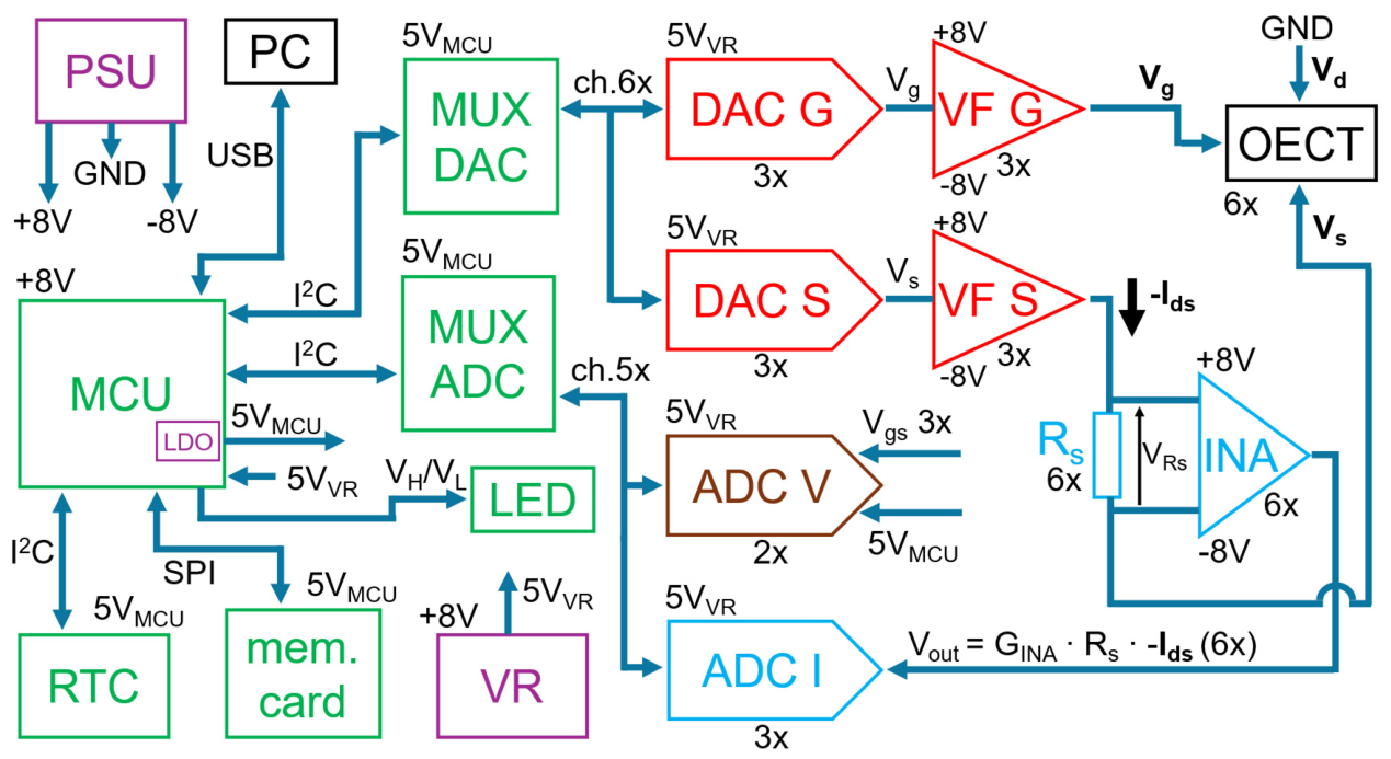
Figure 2.
Electronic schematic of the digital subsystem.
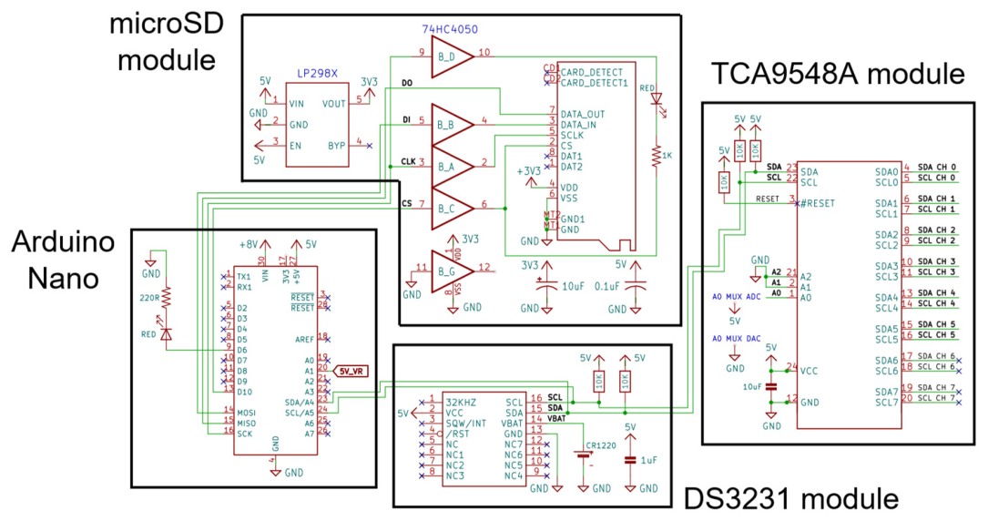
Figure 3.
Electronic schematic of the voltage-driving subsystem. Recurring components are omitted for simplicity.
Figure 3.
Electronic schematic of the voltage-driving subsystem. Recurring components are omitted for simplicity.
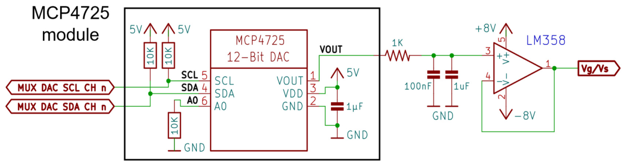
Figure 4.
Electronic schematic of the voltage and current-sensing subsystems. Recurring components are omitted for simplicity.
Figure 4.
Electronic schematic of the voltage and current-sensing subsystems. Recurring components are omitted for simplicity.
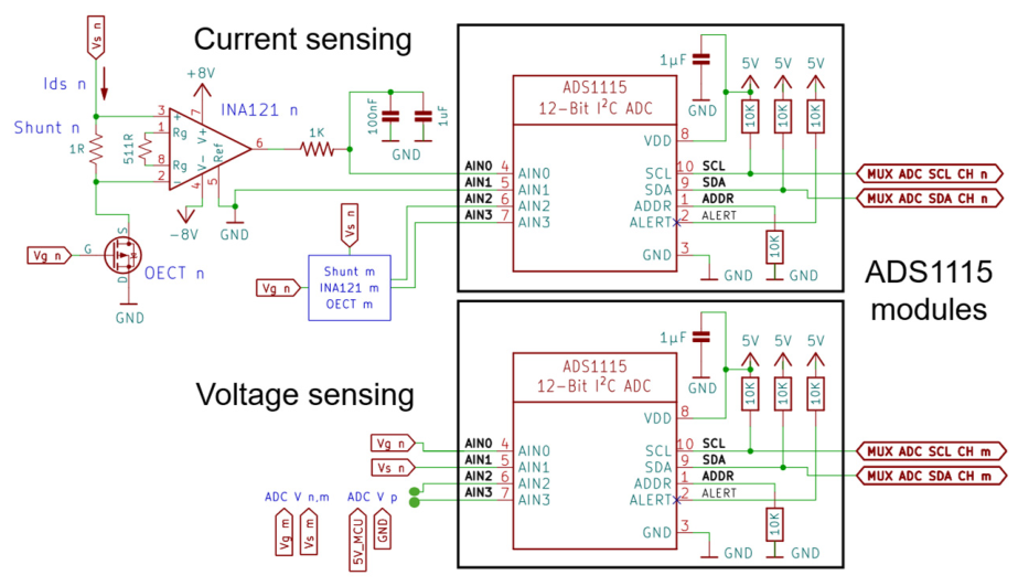
Figure 5.
Electronic schematic of the power supply subsystem.
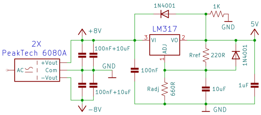
Figure 6.
Design of the OECT set-up, realized with Rhinoceros CAD software.
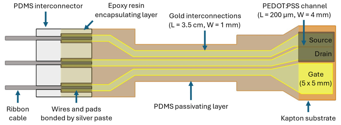
Figure 7.
(A) Assembled SMU circuit in the breadboard. (B) Fabricated OECTs before geometry patterning by laser marking. (C) Developed OECT set-up integrated in the culture plate.
Figure 7.
(A) Assembled SMU circuit in the breadboard. (B) Fabricated OECTs before geometry patterning by laser marking. (C) Developed OECT set-up integrated in the culture plate.
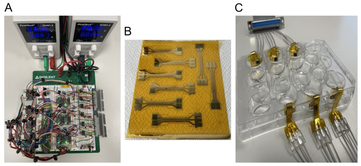
Figure 8.
Execution flow of the developed Arduino programs.
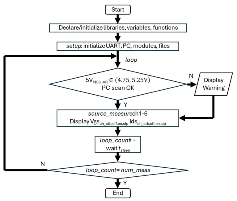
Figure 9.
SMU platform operating in a biological laboratory. The breadboard is connected via ribbon cables to the OECT set-up, placed inside the cell incubator.
Figure 9.
SMU platform operating in a biological laboratory. The breadboard is connected via ribbon cables to the OECT set-up, placed inside the cell incubator.
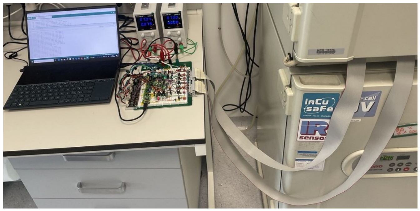
Figure 10.
Residual offset and noise on each channel of the prototype and on B2912A, measured with Rt = 47 Ω, FSR = 20.48 mA, VRt = 0 V, SPS = 128, acquired samples = 70.
Figure 10.
Residual offset and noise on each channel of the prototype and on B2912A, measured with Rt = 47 Ω, FSR = 20.48 mA, VRt = 0 V, SPS = 128, acquired samples = 70.
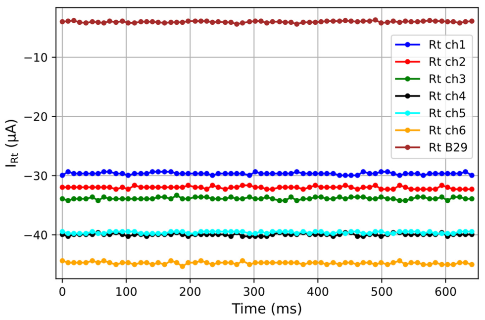
Figure 11.
Test resistor characterization (Rt = 47 Ω) for each channel of the prototype and for B2912A. (A) I – V characterization. VRt = 0 – -0.6 V sweep, FSR = 20.48 mA, SPS = 128, settle time = 200 ms. (B) Transient response characterization. VRt = 0 – -0.6 V step, FSR = 20.48 mA, SPS = 860.
Figure 11.
Test resistor characterization (Rt = 47 Ω) for each channel of the prototype and for B2912A. (A) I – V characterization. VRt = 0 – -0.6 V sweep, FSR = 20.48 mA, SPS = 128, settle time = 200 ms. (B) Transient response characterization. VRt = 0 – -0.6 V step, FSR = 20.48 mA, SPS = 860.
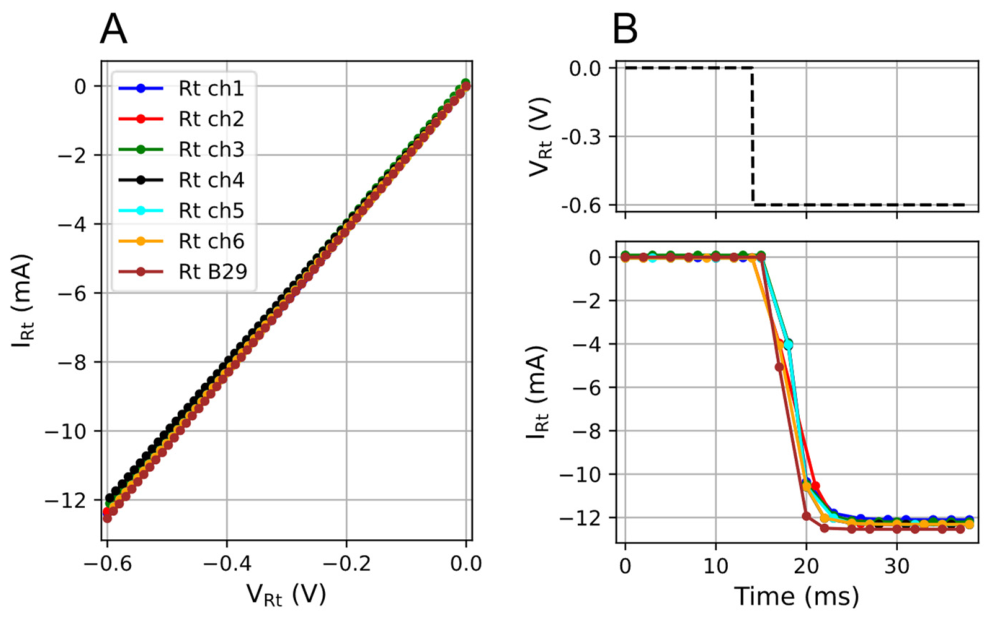
Figure 12.
Ids – Vgs characterization of the six-OECT set-up executed with the developed SMU platform (A) and with B2912A SMU (B). Vgs = 0.6 – 1.2 V (sweep), FSR = 20.48 mA, SPS = 128, settle time = 200 ms, step size = 10 mV.
Figure 12.
Ids – Vgs characterization of the six-OECT set-up executed with the developed SMU platform (A) and with B2912A SMU (B). Vgs = 0.6 – 1.2 V (sweep), FSR = 20.48 mA, SPS = 128, settle time = 200 ms, step size = 10 mV.
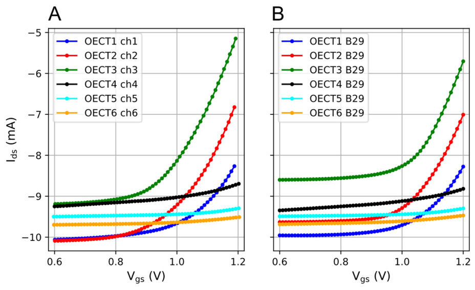
Figure 13.
Transient characterization of the six-OECT set-up executed with the developed SMU platform (A) and with B2912A SMU (B). Vgs = 0.6 – 1.2 V (step), FSR = 20.48 mA, SPS = 860 (sampling = 2.5 ms).
Figure 13.
Transient characterization of the six-OECT set-up executed with the developed SMU platform (A) and with B2912A SMU (B). Vgs = 0.6 – 1.2 V (step), FSR = 20.48 mA, SPS = 860 (sampling = 2.5 ms).
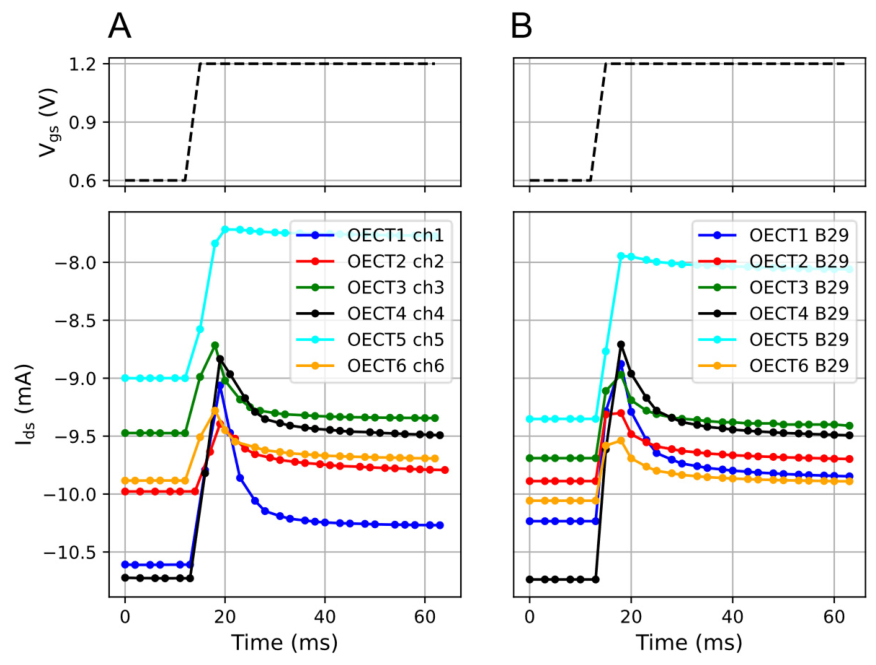
Figure 14.
First and last recorded transient responses for one representative OECT of the set-up in a 5-day continuous experiment. Vgs = 0 – 0.3 V (step), FSR = 20.48 mA, SPS = 860 (sampling = 2.5 ms), acquisition interval = 30 min, experimental period = 5 days.
Figure 14.
First and last recorded transient responses for one representative OECT of the set-up in a 5-day continuous experiment. Vgs = 0 – 0.3 V (step), FSR = 20.48 mA, SPS = 860 (sampling = 2.5 ms), acquisition interval = 30 min, experimental period = 5 days.
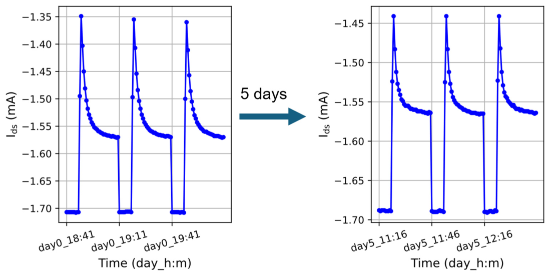
Figure 15.
Ids on values over time extracted from the recorded OECTs transient responses in a 5-day continuous experiment. To simulate the culture medium change, the PBS solution was replaced in the afternoon of the third day. Settings are as the ones reported in the caption of Figure 13.
Figure 15.
Ids on values over time extracted from the recorded OECTs transient responses in a 5-day continuous experiment. To simulate the culture medium change, the PBS solution was replaced in the afternoon of the third day. Settings are as the ones reported in the caption of Figure 13.
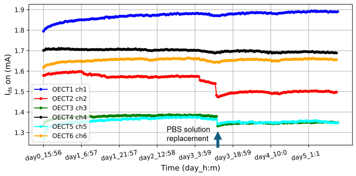
Table 1.
Offset and Gain errors for each subcircuit of the voltage driving and sensing subsystems. Test conditions of each subcircuit are based on converters linear regions and OECT voltage ranges.
Table 1.
Offset and Gain errors for each subcircuit of the voltage driving and sensing subsystems. Test conditions of each subcircuit are based on converters linear regions and OECT voltage ranges.
| Voltage driving / sensing | ∆Offset (mV) | ∆Gain (%) | Conditions |
| Driving Vs_1 | 0 | 1.2 | Offs: Rt = 47 Ω ZS: VZS = 1V, Rt = 100 Ω FS: VFS = 4V, Rt = 470 Ω |
| Driving Vs_2 | 0 | 1.1 | |
| Driving Vs_3 | 0 | 0.3 | |
| Driving Vg_1 | 0 | 0.3 | Open-circuit ZS: VZS = 1V FS: VFS = 4V |
| Driving Vg_2 | 0 | 0.3 | |
| Driving Vg_3 | 0 | 0.4 | |
| Sensing Vgs_1 | 0 | 0.1 | FSR = 6.144 V Open-circuit ZS: VZS = -4V FS: VFS = 4V |
| Sensing Vgs_2 | 0 | 0.1 | |
| Sensing Vgs_3 | 0 | 0.1 | |
| Sensing Power | -1 | 0.1 |
Disclaimer/Publisher’s Note: The statements, opinions and data contained in all publications are solely those of the individual author(s) and contributor(s) and not of MDPI and/or the editor(s). MDPI and/or the editor(s) disclaim responsibility for any injury to people or property resulting from any ideas, methods, instructions or products referred to in the content. |
© 2026 by the authors. Licensee MDPI, Basel, Switzerland. This article is an open access article distributed under the terms and conditions of the Creative Commons Attribution (CC BY) license (http://creativecommons.org/licenses/by/4.0/).
Copyright: This open access article is published under a Creative Commons CC BY 4.0 license, which permit the free download, distribution, and reuse, provided that the author and preprint are cited in any reuse.


