
Submitted:
17 July 2026
Posted:
17 July 2026
You are already at the latest version
Abstract
Directional couplers (DCs) are fundamental building blocks in photonic integrated circuits (PICs), yet achieving their efficient and accurate design in high-dimensional structural design parameter (SDP) spaces remains challenging for existing mode simulation approaches. Here, we propose a machine learning (ML) framework that learns from low-resolution three-dimensional (3D) mode-simulation results, allowing accurate prediction of wavelength-dependent coupling strengths of DCs with high-resolution SDPs across a five-dimensional design space. To improve the cost-effectiveness of training dataset construction, Shapley additive explanations (SHAP) analysis is further introduced to guide the sampling of SDPs. Results show that the ML framework, trained with 1792 samples, completes the prediction of a single structure in ~1 ms and a full-parameter-space sweep in 20 – 35 s, both of which are at least three orders of magnitude faster than 3D mode simulations. In addition, the framework enables inverse design to meet user-defined requirements. The prediction results also show good agreement with experimental results measured from fabricated DCs, achieving absolute deviations (ADs) below 0.05. These results validate the effectiveness of our approach for efficient and accurate DC design in high-dimensional parameter spaces, informing analogous strategies for the design of other photonic devices.
Keywords:
photonic integrated circuits
; machine learning
; directional couplers
I. INTRODUCTION
As the photonic analogue of electronic integrated circuits (EICs) [1,2], photonic integrated circuits (PICs) provide a scalable platform for on-chip optical systems, overcoming the intrinsic bandwidth constraints of EICs and supporting a broad range of applications [3,4]. Directional couplers (DCs), formed by two closely placed waveguides with mutual energy coupling, are essential building blocks in PICs. They constitute functional units such as Mach-Zehnder interferometers [5,6,7], ring resonators [8,9,10], and Sagnac interferometers [11,12,13], as well as more complex PIC systems composed of these units [14].
Despite having simple structures, the efficient and accurate design of DCs remains challenging when sweeping high-dimensional structural design parameter (SDP) spaces and considering wavelength-dependent responses. Conventional approaches for modeling the wavelength-dependent responses of DCs in high-dimensional SDP design spaces typically rely on repeated two-dimensional (2D) or three-dimensional (3D) mode simulations. Although 2D mode simulations are computationally efficient and are widely used for simplified DC analysis, they provide only cross-sectional eigenmode information and cannot accurately capture additional coupling induced by curved waveguides in realistic DC geometries [13,15]. In contrast, 3D simulations can achieve high accuracy by modeling the full 3D geometries of DCs, albeit at the expense of significantly increased computing time and cost [16,17]. Even for a given DC structure at a specific wavelength, a single simulation with normal meshing typically consumes ~300 s. It becomes dramatically more computationally demanding in practical scenarios involving: 1) sweeping high-dimensional SDP spaces for searching target responses and performing inverse design, 2) simulating wavelength-dependent responses, and 3) employing fine meshing to improve simulation accuracy. As a result, realizing these goals in practical DC design requires substantial computational time and resources when using 3D mode simulations.
Recent advances in artificial intelligence (AI) are transforming the modeling and engineering of optical devices [18,19,20,21]. In contrast to traditional simulation methods that depend on iterative solutions of Maxwell equations, AI achieves marked gains in computing efficiency by constructing neural networks that capture the underlying mapping between SDPs and optical responses [22,23,24,25]. This paradigm offers broad applicability and has proven particularly powerful for tackling complex design challenges and optimizing advanced photonic devices [18,19,26,27,28]. In recent years, AI-empowered methods have enabled significant advances in a variety of functional optical devices, such as metasurfaces [25,29,30,31,32], nonlinear optical devices [33,34], electro-optic modulators [35], photodetectors [36,37,38], and quantum optical devices [39,40,41]. In our previous work [42], AI-guided design of 2D-material-based optical polarizers with optimized performance was also explored to significantly reduce computing time while maintaining high accuracy.
Here, we propose a machine learning (ML) framework for DC design in high-dimensional SDP spaces, enabling both high accuracy and low computing time. The framework learns from low-resolution 3D mode-simulation results and predicts the wavelength-dependent coupling strengths of DCs with high-resolution SDPs across a five-dimensional design space. Shapley additive explanations (SHAP) analysis is further introduced to quantify the importance of different SDPs, providing guidance for cost-effective training dataset construction. With 1792 training samples, the trained framework completes the prediction of a single DC structure within ~1 ms and a full-parameter-space sweep within 20–35 s, enabling efficient mapping of the global variation trend across high-dimensional SDP spaces and over a broad wavelength range spanning 1500–1600 nm. The framework also supports inverse design by identifying SDPs that satisfy user-defined design requirements. Experimental results measured from fabricated DCs further confirm the high prediction accuracy, with absolute deviations (ADs) below 0.05. These results highlight the potential of our approach for efficient and accurate DC design in high-dimensional parameter spaces, providing a cost-effective paradigm for ML-guided design of photonic devices.
II. DEVICE STRUCTURE AND MACHINE LEARNING FRAMEWORK
Figure 1(a) shows the schematic of a DC comprising two closely spaced silicon waveguides, where Ein, i and Eout, i (i = 1, 2) denote the input and output optical fields right before and after the DC, respectively. Their relation can be expressed as [13,43,44]:
where j = , λ is the light wavelength, t(λ) and κ(λ) are the field transmission and field coupling coefficients, respectively, satisfying t2(λ) + κ2(λ) = 1 under the lossless coupling approximation. W and H represent the width and height of the silicon waveguide, respectively, and d, L, and R represent the coupling gap, straight coupling length, and bend radius, respectively. These structural parameters govern the evanescent-field interaction between the two waveguides, thereby determining the power transfer and splitting ratio [11,13,45].
Figure 1(b) compares t versus R calculated using the 2D and 3D mode simulation methods for DCs. Here, d = 200 nm, W = 500 nm, H = 220 nm, L = 3 μm, and λ = 1550 nm. The detailed calculation procedure of the 2D mode simulation method is provided in Supplementary Note 1. The t calculated by the 2D method remains almost constant at ~0.99 across the entire R range, whereas the 3D method yields a decrease in t from ~0.98 to ~0.88 as R increases from 5 μm to 80 μm , indicating that the 2D method cannot accurately capture the influence of curved waveguides in realistic DC geometries. Although the 3D mode simulation method provides higher accuracy, even a moderate DC geometry (e.g., d = 180 nm, W = 450 nm, H = 180 nm, L = 5 µm, R = 40 µm) requires ~300 s under the coarsest mesh setting, with the simulation time increasing dramatically with device size and mesh resolution. Such a computing cost is acceptable for isolated device configurations but becomes prohibitive in a high-dimensional SDP space, where many DC geometries need to be simulated across the sampled ranges of d, W, H, L, and R.
As shown in Figure 1(c), the size of the SDP space is defined as the number of discrete SDP vectors, where each vector comprises one sampled value from each SDP. When ten discrete sampled values are assigned to each SDP, the number of SDP vectors increases from 101 to 105 as the dimensionality increases from 1D to 5D. This makes brute-force search computationally expensive, especially when each SDP vector requires a 3D finite-difference time-domain (FDTD) simulation. For example, even with only five sampled values for each SDP, sweeping the full 5D space would require ~37 days of 3D FDTD simulation time, and the cost would further increase with finer mesh resolution.
Figure 1(d) illustrates an ML-based process flow for predicting the wavelength-dependent t’(λ) of DCs with high-resolution SDPs (d’, W’, H’, L’, R’), based on 3D FDTD simulations with low-resolution SDPs (d, W, H, L, R). It consists of three steps. First, 3D FDTD simulations are performed for low-resolution SDPs to obtain t(λ) at M uniformly sampled wavelength points over the wavelength range of 1500–1600 nm. Second, the low-resolution SDPs and corresponding t(λ) are then used to construct the training dataset for the ML framework, which comprises a multilayer perceptron (MLP) and a gated recurrent unit (GRU), as detailed in Supplementary Note 2. Finally, after training, the ML framework predicts t’(λ) for DCs with high-resolution SDPs (d’, W’, H’, L’, R’). For clarity in comparison, t(λ), d, W, H, L, and R refer to the parameters in the training dataset, whereas t’(λ), d’, W’, H’, L’, and R’ correspond to those in the test dataset.
In contrast to exhaustive 3D mode simulation sweeps, this ML-based approach avoids performing 3D FDTD simulations across the high-resolution SDP space. Instead, the trained ML framework uses the learned relationship between the SDPs and t(λ) from a small number of (d, W, H, L, R), to rapidly predict t’(λ) values sampled at M uniformly spaced wavelength points for arbitrary high-resolution SDPs (d’, W’, H’, L’, R’). In addition, performing an exhaustive scan over the high-resolution SDPs using the trained ML framework adds minimal extra time compared with predicting a single SDP vector. For example, predicting t’(λ) for a single SDP vector takes ~0.8–1.5 ms, whereas scanning the full 5D SDP space with five sampled values per SDP, resulting in a test dataset size of 265,837, requires only ~20–35 s, with each additional vector contributing less than 0.15 ms to the total computing time. Beyond the substantial savings in computing time and cost, our method also achieves high prediction accuracy. The ML framework achieves a mean squared error (MSE) as low as ~2.3 × 10⁻⁴ and a coefficient of determination (R2) as high as ~0.98 in predicting t’(λ), using only 1792 low-resolution SDP vectors for training.
III. PERFORMANCE EVALUATION AND DATASET OPTIMIZATION
To account for structural differences and improve prediction accuracy, DCs with different interaction-region geometries are classified into Type-I and Type-II, as detailed in Figure 2(a) and Figure 3(a), respectively. Both types are modeled using the same ML framework architecture shown in Supplementary Note 2, which learns the mapping from the SDPs (d, W, H, L, R) to the wavelength-dependent t(λ). For both types, these SDPs were varied over broad and physically feasible ranges, including d within [100,400] nm, W within [400,640] nm, H within [180,300] nm, L within [0,10] μm, and R within [5,80] μm.
Figure 2 shows the performance of designing Type-I DCs using the ML-based method. Figure 2(a) shows the device schematic of the Type-I DC [13,46,47]. For Type-I DCs, Nd, NW, NH, NL, and NR denote the numbers of sampled values for d, W, H, L, and R, respectively. The low-resolution training dataset was constructed by selecting five equally spaced values for each SDP, with Nd = NW = NH = NL = NR = 5, resulting in a dataset size of N = 55 = 3125. In addition, a high-resolution test dataset was constructed by selecting NW = NH = NR = 13 and Nd = NL = 11 within the same feasible range, resulting in a dataset size of N’ = 265,837. For both datasets, the corresponding FDTD-calculated t(λ) and ML-predicted t’(λ) values were sampled at M = 101 uniformly spaced wavelength points over the wavelength range of 1500–1600 nm to enable a more stringent evaluation of the ML framework’s prediction accuracy.
Figure 2(b) compares t’ versus λ obtained using 3D FDTD and our ML-based method for six randomly sampled test samples (TSs) selected from the high-resolution test dataset. The ML predictions remain consistent with the 3D FDTD results over the wavelength range of 1500–1600 nm. This demonstrates that the trained ML framework can effectively predict t’(λ) by capturing the relationships between the DC SDPs (d, W, H, L, R) and the wavelength-dependent t(λ). The different wavelength-dependent trends mainly arise from geometry-dependent evanescent-field interactions.
To further quantify the agreement observed in Figure 2(b), Figure 2(c) compares the 3D FDTD simulation results t(λ) with the ML predictions t’(λ) over a larger statistical dataset. The data points are obtained from 100 randomly selected TSs from the test dataset. For each TS, t(λ) and t’(λ) are compared at 101 uniformly spaced wavelength points over the wavelength range of 1500–1600 nm, resulting in a total of 10,100 data points. Each dot represents one data point, and the red solid line indicates the diagonal reference. The points for the Type-I DCs cluster closely around the diagonal reference. Figure 2(d) shows the corresponding error distribution, which is centered near zero and exhibits a nearly symmetric profile, with absolute deviations (ADs) below 0.07 for 99% of the data points. These results demonstrate that our ML framework achieves high prediction accuracy and consistency for Type-I DCs.
In addition to the local error distribution analysis above, Figure 2(e) shows the overall performance using MSE and R2 for training, validation, and test datasets. The MSE values are ~4.97×10⁻⁴, ~4.72×10⁻⁴, ~4.92×10⁻⁴ for the training, validation, and test datasets, respectively. The corresponding R2 values are ~0.989, ~0.992, ~0.966, respectively. These MSE and R2 values confirm the high prediction accuracy and generalization capability of the ML framework.

Table I.
VARIOUS TRAINING DATASETS WITH DIFFERENT SAMPLING ALLOCATIONS OF THE ML FRAMEWORK FOR TYPE-I DCS.
Table I.
VARIOUS TRAINING DATASETS WITH DIFFERENT SAMPLING ALLOCATIONS OF THE ML FRAMEWORK FOR TYPE-I DCS.
| Training dataset No. | Nd | NW | NH | NL | NR | N |
| 1 | 5 | 5 | 5 | 5 | 5 | 3125 |
| 2 | 7 | 4 | 4 | 4 | 4 | 1792 |
| 3 | 4 | 7 | 4 | 4 | 4 | 1792 |
| 4 | 4 | 4 | 7 | 4 | 4 | 1792 |
| 5 | 4 | 4 | 4 | 7 | 4 | 1792 |
| 6 | 4 | 4 | 4 | 4 | 7 | 1792 |
Nd, NW, NH, NL, NR are the numbers of sampled values allocated to d, W, H, L, and R, respectively. N is the number of samples in the dataset.
To further interpret the trained ML framework, Figure 2(f) provides the SHAP analysis, where higher normalized SHAP values indicate stronger contributions from the SDPs to the ML framework output [48,49]. The results show that d and W have dominant contributions, with SHAP values of ~0.305 and ~0.255, respectively, much higher than those of H, L, and R. This is consistent with the physics of DCs, since d strongly affects the coupling strength between the two waveguides, and W directly influences the modal effective index and field distribution. Their relatively wide variation ranges, with d from 100 to 400 nm and W from 400 to 640 nm, further enhance their statistical contributions. In contrast, H has a narrower range from 180 to 300 nm, whereas L and R have weaker influence on the coupling strength in the curved waveguide configuration, resulting in lower SHAP values.
Table II.
VARIOUS TRAINING DATASETS WITH DIFFERENT SAMPLING ALLOCATIONS OF THE ML FRAMEWORK FOR TYPE-II DCS.
Table II.
VARIOUS TRAINING DATASETS WITH DIFFERENT SAMPLING ALLOCATIONS OF THE ML FRAMEWORK FOR TYPE-II DCS.
| Training dataset No. | Nd | NW | NH | NL | NR | N |
| 7 | 5 | 5 | 5 | 5 | 5 | 3125 |
| 8 | 7 | 4 | 4 | 4 | 4 | 1792 |
| 9 | 4 | 7 | 4 | 4 | 4 | 1792 |
| 10 | 4 | 4 | 7 | 4 | 4 | 1792 |
| 11 | 4 | 4 | 4 | 7 | 4 | 1792 |
| 12 | 4 | 4 | 4 | 4 | 7 | 1792 |
Nd, NW, NH, NL, NR are the numbers of sampled values allocated to d, W, H, L, and R, respectively. N is the number of samples in the dataset.
Based on the SHAP analysis, we constructed six training datasets with different sampling allocations across the input dimensions to explore training dataset minimization without compromising prediction performance, as detailed in Table I. The training dataset used in Figure 2(c) and 2(d) is denoted as training dataset No. 1. For comparison, training datasets Nos. 2–6 were constructed by assigning seven uniformly sampled values to d, W, H, L, R, respectively, and assigning four uniformly sampled values to each of the remaining four parameters, yielding N = 1792 samples for each training dataset. The same high-resolution test dataset as that used in Figure 2(c) and 2(d) was adopted for evaluation.
The performance of training datasets Nos. 1–6 is evaluated using MSE and R2 in Figure 2(g) and 2(h), with the corresponding scatter plots provided in Supplementary Note 3. Lower MSE and higher R2 values indicate better prediction performance. Training datasets Nos. 1–3 achieve lower MSE and higher R2 values than training datasets Nos. 4–6, with dataset No. 2 showing the best performance, achieving the lowest MSE of ~2.27 × 10⁻⁴ and the highest R2 of ~0.984. Training dataset No. 3 achieves performance comparable to training dataset No. 1, despite using nearly half the number of training samples. These results demonstrate that assigning more sampled values to the high-contribution parameters d and W provides a more efficient strategy for balancing dataset construction cost and prediction performance.
Figure 3(a) shows the schematic of the Type-II DC, which uses a dual-bend interaction region defined by d, R, and L, instead of the curved-straight waveguide layout of the Type-I DC in Figure 2(a) [13,43]. For Type-II DCs, the training datasets were constructed following the same procedure used for Type-I DCs, yielding N = 3125 training samples and N’ = 265,837 test samples. The corresponding t(λ) and t’(λ) values were also sampled at M = 101 uniformly spaced wavelength points over the wavelength range of 1500–1600 nm.
Figure 3(b) compares the 3D-FDTD-simulated and ML-predicted t’(λ) spectra for six randomly selected Type-II DC TSs. Similar to Figure 2(b), the ML-predicted spectra agree well with the 3D-FDTD results over the wavelength range of 1500–1600 nm. This confirms that the trained ML framework can effectively predict t’(λ) for Type-II DCs with a different structural layout.
Figure 3(c) compares the 3D-FDTD-simulated t(λ) and ML-predicted t’(λ) values for Type-II DCs. Similar to the Type-I results in Figure 2(c), the data points are closely distributed around the diagonal reference. The corresponding error distribution in Figure 3(d) is centered near zero, with ADs below 0.06 for 99% of the data points. Figure 3(e) further summarizes the MSE values of ~4.0 × 10⁻⁴, ~4.78 × 10⁻⁴, and ~3.12 × 10⁻⁴ for the training, validation, and test datasets, respectively, with corresponding R2 values of ~0.985, ~0.993, and ~0.967. These results confirm the high prediction accuracy and generalization capability of the trained ML framework for Type-II DCs.
Figure 3(f) provides the SHAP analysis for Type-II DCs. Similar to the Type-I DC results, d and W show the dominant contributions, with SHAP values of ~0.342 and ~0.324, respectively, whereas H, L, and R exhibit lower SHAP values of ~0.082, ~0.191, and ~0.061, respectively. The overall contribution trend is therefore consistent with the Type-I DC results. Compared with Type-I DCs, L shows a higher SHAP value in Type-II DCs, suggesting a slightly increased statistical contribution to the prediction of t’(λ).
To further examine whether the dataset minimization strategy also applies to Type-II DCs, we constructed another six training datasets, Nos. 7–12, with sampling allocations similar to those in Table I, as detailed in Table II. Using the same high-resolution test dataset as that used in Figure 2, Figure 3(g) and 3(h) compare the MSE and R2 values for training datasets Nos. 7–12, and the corresponding scatter plots are provided in Supplementary Note 4. Similar to Figure 2(g) and 2(h), training datasets Nos. 7–9 achieve lower MSE and higher R2 than training datasets Nos. 10–12. Among them, training dataset No. 8 shows the best performance, with the lowest MSE of ~2.25 × 10⁻⁴ and the highest R2 of ~0.976, despite using nearly half as many training samples as training dataset No. 7. These results further demonstrate that allocating more sampled values to high-contribution parameters d and W is a more efficient strategy for balancing training dataset construction cost and prediction performance.
To provide a comprehensive evaluation of our ML-based method, Figure 4 compares its computing time and prediction accuracy under different conditions. Figure 4(a) compares the computing times of the 3D FDTD simulations and the ML-based method for Type-I DCs with different bending radii R. Here, d, W, H, and L are fixed at 200 nm, 500 nm, 220 nm, and 3 μm, respectively, whereas R is varied because it directly changes the device size and has the strongest influence on the simulation-domain size. The 3D FDTD simulations were evaluated under two mesh-accuracy (MA) settings, MA = 1 and MA = 5, corresponding to coarse and high-accuracy mesh settings, respectively. Specifically, MA = 1 represents a coarse mesh setting, whereas MA = 5 represents a high-accuracy mesh setting selected within the available computational-resource limit. For the ML-based method, MA refers to the mesh accuracy used to generate the 3D-FDTD training data rather than a setting used during ML inference. All computations were carried out on the same computer equipped with an Intel(R) Xeon(R) CPU E5-1650 v4 running at 3.60 GHz and 32.0 GB of RAM.
As shown in Figure 4(a), for a single SDP of Type-I DCs, the computing time of 3D FDTD simulation increases as R increases from 5 μm to 80 μm. For MA = 1, the computing time increases from ~25 s to ~1440 s as R increases, whereas for MA = 5, it increases from ~50 s to ~28,409 s. This increase mainly arises from the enlarged simulation domain and the increased number of mesh elements required for numerical solving at larger R. In contrast, under both MA = 1 and MA = 5 cases, the ML-based method requires only ~0.8–1.5 ms for Type-I DCs, and the computing times remain nearly unchanged with increasing R. Compared with 3D FDTD simulations, our approach reduces the overall computing time by four to seven orders of magnitude, depending on the specific R and MA conditions. These results indicate that, unlike the 3D FDTD simulation, whose computing time strongly depends on device size and mesh accuracy, the ML-based method is largely insensitive to device size and enables rapid prediction across different SDP vectors. A similar trend is observed for Type-II DCs. At R = 80 μm, the ML-based method requires only ~1.2 ms under both MA settings, whereas the 3D FDTD computing time reaches ~2379 s for MA = 1 and ~56,500 s for MA = 5. To visualize the difference between the two mesh-accuracy settings used in Figure 4(a), Figure 4(b) shows the corresponding top-view schematics and zoom-in views of the DC geometry. MA = 1 exhibits a jagged device boundary due to the coarse mesh, but MA = 5 produces a smooth boundary resulting from the finer mesh.
Figure 4(c) shows the overall computing time versus test dataset size of our ML-based method. The overall computing time refers to the total time required to predict t’(λ) for all SDP vectors in the test dataset. As the test dataset size increases from 101 to 105, the overall computing time ranges from ~0.8 to ~26 s, remaining within a low time range. Notably, even when the test dataset size reaches 265,837 vectors, the total computing time is still less than ~30 s. This highlights that the ML-based method maintains high-speed prediction even for large test datasets, whereas the 3D FDTD computing time would accumulate approximately linearly with dataset size.
Analyses of training dataset size, GRU layer number, and MLP layer number for both Type-I and Type-II DCs are provided in Supplementary Note 5. For both types, increasing the training dataset size decreases the MSE and increases R2, but also increases the dataset-construction cost. In contrast, increasing the number of GRU or MLP layers leads to only limited improvement. Considering the trade-off between prediction performance and dataset-construction cost, 3125 training samples were selected for both Type-I and Type-II DCs. In addition, one GRU layer and two MLP layers were selected for the ML frameworks used for both types of DCs.
IV. INVERSE DESIGN
Beyond forward prediction, the trained ML framework is further used for target-oriented inverse design. In inverse design, the design direction is reversed from response prediction to structure identification, where the objective is to determine suitable SDP vectors that produce the desired optical response. Here, instead of specifying a complete target spectrum, the design target is described by several spectral design criteria, including the target t value (tref) at the fixed reference wavelength of 1550 nm, the required variation of t over the investigated wavelength range (Δt), and the required wavelength-dependent trend. Details of the inverse-design process are provided in Supplementary Note 6.
Figure 5(a) presents the target-oriented inverse-design results for Type-I DCs, where d, L, and R are treated as design variables, and W and H are fixed at 400 nm and 220 nm, respectively. This setting reflects practical device design, where some SDPs can be fixed according to the fabrication platform, layout constraints, or predefined design requirements. Three inverse-design examples (IDEs) are considered with different spectral design criteria, and the selected SDP vectors all achieve combined deviations below the preset threshold of 0.01. IDE1 is designed to achieve increasing t for increasing wavelength over the range of 1500–1600 nm, whereas IDE2 and IDE3 target decreasing t for increasing wavelength. For IDE1–IDE3, tref is set to 0.858, 0.977, and 0.884 at 1550 nm, respectively, and Δt is set to 0.45, 0.023, and 0.13, respectively. The 3D-FDTD-calculated results agree well with the ML-predicted responses, confirming that the inverse-designed SDPs can generate the designed optical responses for Type-I DCs.
Figure 5(b) presents the corresponding inverse-design results for Type-II DCs under the same design-variable setting. Similar to those in Figure 5(a), IDE4 is designed to achieve increasing t for increasing wavelength, whereas IDE5 and IDE6 target decreasing t for increasing wavelength. For IDE4–IDE6, tref is set to 0.875, 0.988, and 0.835 at 1550 nm, respectively, and Δt is set to 0.404, 0.013, and 0.202, respectively. The 3D-FDTD-calculated results also show good agreement with the ML-predicted responses, further verifying the feasibility of inverse design of Type-II DCs based on our ML approach.
Figure 5(c) shows the inverse-design results for Type-I DCs, where d, W, L, and R are treated as design variables, and H is fixed at 220 nm. IDE7 is designed to achieve increasing t for increasing wavelength, whereas IDE8 and IDE9 target decreasing t for increasing wavelength. For IDE7–IDE9, tref is set to 0.885, 0.975, and 0.871, respectively, and Δt is set to 0.413, 0.013, and 0.151, respectively. The 3D-FDTD-calculated results remain close to the ML-predicted responses, confirming that the inverse-design process remains reliable when W is additionally included as a design variable.
Figure 5(d) shows the corresponding inverse-design results for Type-II DCs under the same design-variable setting as that used in Figure 5(c). IDE10 is designed to achieve increasing t for increasing wavelength, whereas IDE11 and IDE12 target decreasing t for increasing wavelength. For IDE10–IDE12, tref is set to 0.883, 0.999, and 0.876, respectively, and Δt is set to 0.404, 0.003, and 0.15, respectively. Similar agreement between the ML-predicted and 3D-FDTD-calculated results is obtained.
According to the computing-time analysis in Figure 4, the 3D FDTD cost accumulates rapidly in target-oriented search because each SDP vector requires an independent simulation. For the inverse-design examples in Figure 5(a) and 5(b), reaching the same search resolution in the three-variable SDP space would require 2160 independent 3D FDTD simulations, corresponding to ~25 days of computing time. For the four-variable cases in Figure 5(c) and 5(d), this increases to at least 32,400 simulations, corresponding to ~380 days. These costs would increase further if all five SDPs were used as design variables or if finer sampling were required. In contrast, the ML-based inverse-design process identifies the target SDP vectors within two to three search iterations, with the total search time remaining below 2 min.
V. EXPERIMENTAL VALIDATION
To experimentally validate both the forward-prediction capability and target-oriented inverse-design feasibility of the ML framework, we fabricated Type-I and Type-II DCs and compared the experimental results with those predicted by the ML framework. Figure 6(a) shows microscopic images of the fabricated Type-I and Type-II DCs. Details of device fabrication and experimental t extraction are provided in Supplementary Note 7.
Figure 6(b) compares the experimentally extracted t values with those predicted by the ML framework for Type-I DCs over the wavelength range of 1535–1565 nm. In each comparison, only one SDP is varied, and the remaining parameters are fixed at d = 200 nm, W = 500 nm, H = 220 nm, L = 3 μm, and R = 20 μm.
Figure 6(b-i) compares t versus λ obtained from experimental (Exp.) extraction and our ML-based method for Type-I DCs under varying d. The ML-framework predictions closely follow the experimentally extracted results for all three d values, with average ADs below 0.03, confirming that the model accurately captures the gap-dependent variation of t(λ). As d increases from 160 nm to 200 nm, t increases across the wavelength range, mainly because a larger gap weakens the evanescent-field interaction between the two waveguides and reduces power transfer to the cross port.
Figure 6(b-ii) shows the corresponding results under varying W, where the predictions agree well with the extracted results, with average ADs below 0.03. As W increases from 400 nm to 500 nm, t increases across the wavelength range and its wavelength dependence decreases, which can be attributed to stronger lateral confinement, reduced evanescent-field overlap, and lower wavelength sensitivity of the modal field distribution.
Figure 6(b-iii) shows the corresponding results under varying L, with average ADs below 0.04. As L increases from 1 μm to 5 μm, t decreases across the wavelength range because a longer interaction length enables more power transfer between the two waveguides. The wavelength-dependent variation of t also becomes more noticeable at larger L, since the wavelength-dependent power transfer accumulates over a longer interaction region.
Figure 6(b-iv) shows the corresponding results under varying R, with average ADs below 0.03. As R increases from 10 μm to 40 μm, t decreases across the wavelength range, mainly because a larger bending radius reduces bend-induced mode distortion and allows more efficient power transfer between the two waveguides.
Figure 6(c-i) – 6(c-iv) show the corresponding results for Type-II DCs under varying parameters d, W, L, and R, respectively, using the same SDP settings as those in Figure 6(b-i) – 6(b-iv). For clarity, one data point extracted from every four resonance notches within the wavelength range is displayed in the plots, and the full extracted data are used for the comparison and error analysis. Similar trends are observed, where t increases with increasing d and W, but decreases with increasing L and R. The wavelength-dependent variation of t becomes more noticeable at smaller W and larger L, consistent with the Type-I DC results. The ML-framework predictions agree well with the experimentally extracted results for all investigated SDPs, with average ADs below 0.05.
To experimentally validate the target-oriented inverse-design capability, we specified the spectral design criteria and used the trained ML framework to select the corresponding SDPs. Additional test devices containing Type-I and Type-II DCs with the inverse-designed SDPs were fabricated and characterized. In these devices, W and H were fixed at 400 nm and 220 nm, respectively, and d, L, and R were determined by the inverse-design process.
Figure 7(a) compares the experimentally extracted and ML-predicted results for three inverse-designed Type-I DCs. All three inverse-design examples (IDEs) are designed to achieve decreasing t for increasing wavelength over the range of 1535–1565 nm. For IDE13–IDE15, tref is set to 0.947, 0.89, and 0.852 at 1550 nm, respectively, and Δt is set to 0.017, 0.04, and 0.056, respectively. The experimental results agree well with the ML-predicted responses, with average ADs below 0.04. This confirms that the fabricated Type-I DCs with inverse-designed SDPs can effectively generate the designed optical responses.
Figure 7(b) shows the corresponding results for three inverse-designed Type-II DCs. Similar to those in Figure 7(a), all three IDEs target decreasing t for increasing wavelength. For IDE16–IDE18, tref is set to 0.947, 0.904, and 0.869, respectively, and Δt is set to 0.017, 0.035, and 0.038, respectively. The experimental results also show good agreement with the ML-predicted responses, with average ADs below 0.04, further verifying the feasibility of inverse design of Type-II DCs based on our ML approach. This work has broad implications for microcombs [50,51,52,53,54,55,56,57,58,59,60,61,62,63,64,65,66,67,68,69,70,71,72,73,74,75,76,77,78,79,80] and their applications to microwave photonics, neuromorphic processors and communications. [81,82,83,84,85,86,87,88,89,90,91,92,93,94,95,96,97,98,99,100,101,102,103,104,105,106,107,108,109,110,111,112,113,114,115,116,117,118,119,120,121,122,123,124,125,126,127,128,129,130,131,132,133,134,135] The addition and use of 2D materials [136,137,138,139,140,141,142,143,144,145,146,147,148,149,150,151,152,153,154,155,156,157,158,159,160,161,162,163,164,165,166,167,168,169,170,171,172,173,174,175,176,177,178] will add extra functionality to microcomb chips for potential applications to quantum photonics [179,180,181,182,183,184,185,186,187,188,189,190,191,192,193,194] and other areas. [195,196,197,198,199,200,201,202,203,204,205,206,207,208,209,210,211,212]
VI. CONCLUSION
In summary, an ML framework is developed for photonic integrated DC design in high-dimensional SDP spaces, featuring both high accuracy and low computing time. By learning from low-resolution 3D mode-simulation results, the framework can predict wavelength-dependent coupling strengths of DCs with high-resolution SDPs across a five-dimensional design space. SHAP analysis is emp[81–135loyed to guide the sampling of SDPs, thereby improving the cost-effectiveness for constructing the training datasets. After training on 1792 samples, the framework completes the prediction of a single DC structure within ~1 ms and a full-parameter-space sweep over the 1500–1600 nm wavelength range within 20–35 s, both of which are at least three orders of magnitude faster than 3D mode simulations. Beyond forward prediction, the trained framework supports inverse design by identifying SDPs that satisfy user-defined design requirements. The prediction results also show good agreement with experimental results measured from fabricated DCs, achieving ADs below 0.05. Our approach provides a new route towards accurate and efficient DC design in high-dimensional parameter spaces. Given the fundamental role of DCs in PICs, it also has strong potential to be extended to the design of other functional units and more complex PIC systems.
References
- J. E. Green, J. Wook Choi, A. Boukai, Y. Bunimovich, E. Johnston Halperin, E. DeIonno, Y. Luo, B. A. Sheriff, K. Xu, Y. Shik Shin, H. R. Tseng, J. F. Stoddart, and J. R. Heath, “A 160-kilobit molecular electronic memory patterned at 1011 bits per square centimetre,” Nature, vol. 445, no. 7126, pp. 414–417, 2007/01/01, 2007. [CrossRef]
- C. Xiang, and J. E. Bowers, “Building 3D integrated circuits with electronics and photonics,” Nature Electronics, vol. 7, no. 6, pp. 422–424, 2024/06/01, 2024. [CrossRef]
- S. Hua, E. Divita, S. Yu, B. Peng, C. Roques Carmes, Z. Su, Z. Chen, Y. Bai, J. Zou, Y. Zhu, Y. Xu, C. k. Lu, Y. Di, H. Chen, L. Jiang, L. Wang, L. Ou, C. Zhang, J. Chen, W. Zhang, H. Zhu, W. Kuang, L. Wang, H. Meng, M. Steinman, and Y. Shen, “An integrated large-scale photonic accelerator with ultralow latency,” Nature, vol. 640, no. 8058, pp. 361–367, 2025/04/01, 2025. [CrossRef]
- C. Sun, M. T. Wade, Y. Lee, J. S. Orcutt, L. Alloatti, M. S. Georgas, A. S. Waterman, J. M. Shainline, R. R. Avizienis, S. Lin, B. R. Moss, R. Kumar, F. Pavanello, A. H. Atabaki, H. M. Cook, A. J. Ou, J. C. Leu, Y. H. Chen, K. Asanović, R. J. Ram, M. A. Popović, and V. M. Stojanović, “Single-chip microprocessor that communicates directly using light,” Nature, vol. 528, no. 7583, pp. 534–538, 2015/12/01, 2015. [CrossRef]
- C. Sturm, D. Tanese, H. S. Nguyen, H. Flayac, E. Galopin, A. Lemaître, I. Sagnes, D. Solnyshkov, A. Amo, G. Malpuech, and J. Bloch, “All-optical phase modulation in a cavity-polariton Mach-Zehnder interferometer,” Nature Communications, vol. 5, no. 1, pp. 3278, 2014/02/11, 2014. [CrossRef]
- J. Bütow, J. S. Eismann, V. Sharma, D. Brandmüller, and P. Banzer, “Generating free-space structured light with programmable integrated photonics,” Nature Photonics, vol. 18, no. 3, pp. 243–249, 2024/03/01, 2024. [CrossRef]
- M. H. Idjadi, K. Kim, and N. K. Fontaine, “Modulation-free laser stabilization technique using integrated cavity-coupled Mach-Zehnder interferometer,” Nature Communications, vol. 15, no. 1, pp. 1922, 2024/03/01, 2024. [CrossRef]
- J. Wu, Y. Yang, Y. Qu, L. Jia, Y. Zhang, X. Xu, S. T. Chu, B. E. Little, R. Morandotti, B. Jia, and D. J. Moss, “2D Layered Graphene Oxide Films Integrated with Micro-Ring Resonators for Enhanced Nonlinear Optics,” Small, vol. 16, no. 16, pp. 1906563, 2020/04/01, 2020. [CrossRef]
- D. Kazakov, T. P. Letsou, M. Beiser, Y. Zhi, N. Opačak, M. Piccardo, B. Schwarz, and F. Capasso, “Active mid-infrared ring resonators,” Nature Communications, vol. 15, no. 1, pp. 607, 2024/01/19, 2024. [CrossRef]
- B. Yao, S. W. Huang, Y. Liu, A. K. Vinod, C. Choi, M. Hoff, Y. Li, M. Yu, Z. Feng, D. L. Kwong, Y. Huang, Y. Rao, X. Duan, and C. W. Wong, “Gate-tunable frequency combs in graphene–nitride microresonators,” Nature, vol. 558, no. 7710, pp. 410–414, 2018/06/01, 2018. [CrossRef]
- J. Wu, T. Moein, X. Xu, and D. J. Moss, “Advanced photonic filters based on cascaded Sagnac loop reflector resonators in silicon-on-insulator nanowires,” APL Photonics, vol. 3, no. 4, 2018.
- E. J. Post, “Sagnac Effect,” Reviews of Modern Physics, vol. 39, no. 2, pp. 475–493, 04/01/, 1967.
- H. Arianfard, S. Juodkazis, D. J. Moss, and J. Wu, “Sagnac interference in integrated photonics,” Applied Physics Reviews, vol. 10, no. 1, 2023.
- S. Bandyopadhyay, R. Hamerly, and D. Englund, “Hardware error correction for programmable photonics,” The Optical Society, 2021. [CrossRef]
- “Fundamental Building Blocks,” Silicon photonics design: from devices to systems, L. Chrostowski and M. Hochberg, eds., pp. 92–161, Cambridge: Cambridge University Press, 2015.
- G. Tang, X. Chen, L. Sun, C. Guo, M. Li, Z. Tian, H. Chen, H. Wang, Q. Sun, Y. Pan, X. He, Y. Su, and J. Dong, “Broadband and fabrication-tolerant 3-dB couplers with topological valley edge modes,” Light: Science & Applications, vol. 13, no. 1, pp. 166, 2024/07/16, 2024. [CrossRef]
- F. Li, X. Hu, J. Wu, L. Zhou, and Y. Su, “Ultra-compact and broadband orthogonal coupler between strip and slot silicon waveguides.” pp. 1–6.
- W. Ma, Z. Liu, Z. A. Kudyshev, A. Boltasseva, W. Cai, and Y. Liu, “Deep learning for the design of photonic structures,” Nature photonics, vol. 15, no. 2, pp. 77–90, 2021.
- J. Jiang, M. Chen, and J. Fan, “Deep neural networks for the evaluation and design of photonic devices,” Nature Reviews Materials, vol. 6, 12/17, 2020. [CrossRef]
- S. Molesky, Z. Lin, A. Y. Piggott, W. Jin, J. Vucković, and A. W. Rodriguez, “Inverse design in nanophotonics,” Nature Photonics, vol. 12, no. 11, pp. 659–670, 2018/11/01, 2018.
- J. Yang, M. A. Guidry, D. M. Lukin, K. Yang, and J. Vučković, “Inverse-designed silicon carbide quantum and nonlinear photonics,” Light: Science & Applications, vol. 12, no. 1, pp. 201, 2023/08/22, 2023. [CrossRef]
- J. Peurifoy, Y. Shen, L. Jing, Y. Yang, F. Cano-Renteria, B. G. DeLacy, J. D. Joannopoulos, M. Tegmark, and M. Soljačić, “Nanophotonic particle simulation and inverse design using artificial neural networks,” Science Advances, vol. 4, no. 6, pp. eaar4206, 2018. [CrossRef]
- Y. Xu, X. Zhang, Y. Fu, and Y. Liu, “Interfacing Photonics with Artificial Intelligence: A New Design Strategy for Photonic Structures and Devices based on Artificial Neural Networks,” Photonics Research, vol. 9, 02/05, 2021. [CrossRef]
- X. Xu, M. Tan, B. Corcoran, J. Wu, A. Boes, T. G. Nguyen, S. T. Chu, B. E. Little, D. G. Hicks, R. Morandotti, A. Mitchell, and D. J. Moss, “11 TOPS photonic convolutional accelerator for optical neural networks,” Nature, vol. 589, no. 7840, pp. 44–51, 2021/01/01, 2021. [CrossRef]
- Malkiel, M. Mrejen, A. Nagler, U. Arieli, L. Wolf, and H. Suchowski, “Plasmonic nanostructure design and characterization via Deep Learning,” Light: Science & Applications, vol. 7, no. 1, pp. 60, 2018/09/05, 2018. [CrossRef]
- N. Mohammadi Estakhri, B. Edwards, and N. Engheta, “Inverse-designed metastructures that solve equations,” Science, vol. 363, no. 6433, pp. 1333–1338, 2019/03/22, 2019. [CrossRef]
- M. He, J. R. Nolen, J. Nordlander, A. Cleri, N. S. McIlwaine, Y. Tang, G. Lu, T. G. Folland, B. A. Landman, and J.-P. Maria, “Deterministic inverse design of Tamm plasmon thermal emitters with multi-resonant control,” Nature materials, vol. 20, no. 12, pp. 1663–1669, 2021. [CrossRef]
- C. Dory, D. Vercruysse, K. Y. Yang, N. V. Sapra, A. E. Rugar, S. Sun, D. M. Lukin, A. Y. Piggott, J. L. Zhang, M. Radulaski, K. G. Lagoudakis, L. Su, and J. Vučković, “Inverse-designed diamond photonics,” Nature Communications, vol. 10, no. 1, pp. 3309, 2019/07/25, 2019. [CrossRef]
- Ueno, J. Hu, and S. An, “AI for optical metasurface,” npj Nanophotonics, vol. 1, no. 1, pp. 36, 2024/09/02, 2024. [CrossRef]
- R. Zhu, T. Qiu, J. Wang, S. Sui, C. Hao, T. Liu, Y. Li, M. Feng, A. Zhang, C.-W. Qiu, and S. Qu, “Phase-to-pattern inverse design paradigm for fast realization of functional metasurfaces via transfer learning,” Nature Communications, vol. 12, no. 1, pp. 2974, 2021/05/20, 2021. [CrossRef]
- E. Zhu, Z. Zong, E. Li, Y. Lu, J. Zhang, H. Xie, Y. Li, W.-Y. Yin, and Z. Wei, “Frequency transfer and inverse design for metasurface under multi-physics coupling by Euler latent dynamic and data-analytical regularizations,” Nature Communications, vol. 16, no. 1, pp. 2251, 2025/03/06, 2025. [CrossRef]
- Z. Liu, D. Zhu, S. P. Rodrigues, K.-T. Lee, and W. Cai, “Generative Model for the Inverse Design of Metasurfaces,” Nano Letters, vol. 18, no. 10, pp. 6570–6576, 2018/10/10, 2018. [CrossRef]
- Q. Fan, G. Zhou, T. Gui, C. Lu, and A. P. T. Lau, “Advancing theoretical understanding and practical performance of signal processing for nonlinear optical communications through machine learning,” Nature Communications, vol. 11, no. 1, pp. 3694, 2020/07/23, 2020. [CrossRef]
- G. Genty, L. Salmela, J. M. Dudley, D. Brunner, A. Kokhanovskiy, S. Kobtsev, and S. K. Turitsyn, “Machine learning and applications in ultrafast photonics,” Nature Photonics, vol. 15, no. 2, pp. 91–101, 2021/02/01, 2021. [CrossRef]
- R. Aparecido de Paula, I. Aldaya, T. Sutili, R. C. Figueiredo, J. L. Pita, and Y. R. R. Bustamante, “Design of a silicon Mach-Zehnder modulator via deep learning and evolutionary algorithms,” Scientific Reports, vol. 13, no. 1, pp. 14662, 2023/09/05, 2023. [CrossRef]
- S. B. Choi, J. S. Choi, H. S. Shin, J.-W. Yoon, Y. Kim, and J.-W. Kim, “Deep learning-developed multi-light source discrimination capability of stretchable capacitive photodetector,” npj Flexible Electronics, vol. 9, no. 1, pp. 44, 2025/05/15, 2025. [CrossRef]
- R. A. W. Ayyubi, M. X. Low, S. Salimi, M. Khorsandi, M. M. Hossain, H. Arooj, S. Masood, M. H. Zeb, N. Mahmood, Q. Bao, S. Walia, and B. Shabbir, “Machine learning-assisted high-throughput prediction and experimental validation of high-responsivity extreme ultraviolet detectors,” Nature Communications, vol. 16, no. 1, pp. 6265, 2025/07/07, 2025. [CrossRef]
- S. Oh, H. Kim, M. Meyyappan, and K. Kim, “Design and Analysis of Near-IR Photodetector Using Machine Learning Approach,” IEEE Sensors Journal, vol. 24, no. 16, pp. 25565–25572, 2024. [CrossRef]
- Z. A. Kudyshev, D. Sychev, Z. Martin, O. Yesilyurt, S. I. Bogdanov, X. Xu, P.-G. Chen, A. V. Kildishev, A. Boltasseva, and V. M. Shalaev, “Machine learning assisted quantum super-resolution microscopy,” Nature Communications, vol. 14, no. 1, pp. 4828, 2023/08/10, 2023.
- Z. A. Kudyshev, V. M. Shalaev, and A. Boltasseva, “Machine Learning for Integrated Quantum Photonics,” ACS Photonics, vol. 8, no. 1, pp. 34–46, 2021/01/20, 2021. [CrossRef]
- G. Torlai, G. Mazzola, J. Carrasquilla, M. Troyer, R. Melko, and G. Carleo, “Neural-network quantum state tomography,” Nature Physics, vol. 14, no. 5, pp. 447–450, 2018/05/01, 2018. [CrossRef]
- R. Wang, D. Jin, J. Hu, W. Liu, Y. Zhang, I. H. Abidi, S. Walia, B. Jia, D. Huang, J. Wu, and D. J. Moss, “AI-guided design and optimization of 2D-material-based optical polarizers,” Chip, pp. 100196, 2026/02/17/, 2026. [CrossRef]
- D. Jin, S. Ren, J. Hu, D. Huang, D. J. Moss, and J. Wu, “Modeling of Complex Integrated Photonic Resonators Using the Scattering Matrix Method,” Photonics, vol. 11, no. 12, 2024. [CrossRef]
- Yariv, “Universal relations for coupling of optical power between microresonators and dielectric waveguides,” Electronics Letters, vol. 36, pp. 321–322, 2000.
- X. Xu, Z. Xie, J. Zheng, J. Liang, T. Zhong, M. Yu, S. Kocaman, G. Q. Lo, D. L. Kwong, D. R. Englund, F. N. C. Wong, and C. W. Wong, “Near-infrared Hong-Ou-Mandel interference on a silicon quantum photonic chip,” Optics express, vol. 21 4, pp. 5014–24, 2012. [CrossRef]
- W. Bogaerts, P. De Heyn, T. Van Vaerenbergh, K. De Vos, S. Kumar Selvaraja, T. Claes, P. Dumon, P. Bienstman, D. Van Thourhout, and R. Baets, “Silicon microring resonators,” Laser & Photonics Reviews, vol. 6, no. 1, pp. 47–73, 2012/01/02, 2012.
- S. Feng, T. Lei, H. Chen, H. Cai, X. Luo, and A. W. Poon, “Silicon photonics: from a microresonator perspective,” Laser & Photonics Reviews, vol. 6, no. 2, pp. 145–177, 2012/04/01, 2012. [CrossRef]
- N. Bar, T. Korem, O. Weissbrod. The, “A reference map of potential determinants for the human serum metabolome,” Nature, vol. 588, no. 7836, pp. 135–140, 2020/12/01, 2020.
- S. M. Lundberg, and S.-I. Lee, “A unified approach to interpreting model predictions,” in Proceedings of the 31st International Conference on Neural Information Processing Systems, Long Beach, California, USA, 2017, pp. 4768–4777.
- Moss, D. J., Morandotti, R., Gaeta, A. L. & Lipson, M. New CMOS compatible platforms based on silicon nitride and Hydex for nonlinear optics. Nat. Photonics Vol. 7, 597-607 (2013). [CrossRef]
- L. Razzari, et al., “CMOS-compatible integrated optical hyper-parametric oscillator,” Nature Photonics, vol. 4, no. 1, pp. 41-45, 2010.
- Pasquazi, et al., “Sub-picosecond phase-sensitive optical pulse characterization on a chip”, Nature Photonics, vol. 5, no. 10, pp. 618-623 (2011). [CrossRef]
- M Ferrera et al., “On-Chip ultra-fast 1st and 2nd order CMOS compatible all-optical integration”, Optics Express vol. 19 (23), 23153-23161 (2011).
- Bao, C., et al., Direct soliton generation in microresonators, Opt. Lett, 42, 2519 (2017).
- M.Ferrera et al., “CMOS compatible integrated all-optical RF spectrum analyzer”, Optics Express, vol. 22, no. 18, 21488 - 21498 (2014).
- M. Kues, et al., “Passively modelocked laser with an ultra-narrow spectral width”, Nature Photonics, vol. 11, no. 3, 159 (2017).
- M. Ferrera, et al., “Low-power continuous-wave nonlinear optics in doped silica glass integrated waveguide structures,” Nature Photonics, vol. 2, no. 12, pp. 737-740, 2008. [CrossRef]
- M.Ferrera et al.”On-Chip ultra-fast 1st and 2nd order CMOS compatible all-optical integration”, Opt. Express, vol. 19, (23)pp. 23153-23161 (2011).
- D. Duchesne, M. Peccianti, M. R. E. Lamont, et al., “Supercontinuum generation in a high index doped silica glass spiral waveguide,” Optics Express, vol. 18, no, 2, pp. 923-930, 2010. [CrossRef]
- H Bao et al., “Turing patterns in a fiber laser with a nested microresonator: Robust and controllable microcomb generation”, Physical Review Research vol. 2 (2), 023395 (2020). [CrossRef]
- M. Ferrera, et al., “On-chip CMOS-compatible all-optical integrator”, Nature Communications, vol. 1, Article 29 (2010). [CrossRef]
- Pasquazi, et al., “All-optical wavelength conversion in an integrated ring resonator,” Optics Express, vol. 18, no. 4, 3858-3863 (2010). [CrossRef]
- Pasquazi, Y. Park, J. Azana, et al., “Efficient wavelength conversion and net parametric gain via Four Wave Mixing in a high index doped silica waveguide,” Optics Express, vol. 18, no. 8, pp. 7634-7641 (2010).
- Peccianti, M. Ferrera, L. Razzari, et al., “Subpicosecond optical pulse compression via an integrated nonlinear chirper,” Optics Express, vol. 18, no. 8, pp. 7625-7633 (2010). [CrossRef]
- M. Ferrera et al., “All-optical 1st and 2nd order integration on a chip”, Optics Express vol. 19 (23), 23153-23161 (2011). [CrossRef]
- M. Ferrera et al., “Low Power CW Parametric Mixing in a Low Dispersion High Index Doped Silica Glass Micro-Ring Resonator with Q-factor > 1 Million”, Optics Express, vol.17, no. 16, 14098–14103 (2009).
- M. Peccianti, et al., “Demonstration of an ultrafast nonlinear microcavity modelocked laser”, Nature Communications, vol. 3, 765, 2012.
- Pasquazi, et al., “Self-locked optical parametric oscillation in a CMOS compatible microring resonator: a route to robust optical frequency comb generation on a chip,” Optics Express, vol. 21, no. 11, 13333-13341 (2013). [CrossRef]
- Pasquazi, et al., “Stable, dual mode, high repetition rate mode-locked laser based on a microring resonator,” Optics Express, vol. 20, no. 24, 27355-27362 (2012). [CrossRef]
- Pasquazi, A. et al. “Micro-combs: a novel generation of optical sources”, Physics Reports 729, 1-81 (2018). [CrossRef]
- H. Bao, et al., “Laser cavity-soliton microcombs”, Nature Photonics, vol. 13, no. 6, 384-389, (2019). [CrossRef]
- Cutrona et al., “High Conversion Efficiency in Laser Cavity-Soliton Microcombs”, Optics Express Vol. 30, Issue 22, 39816-39825 (2022).
- M. Rowley et al., “Self-emergence of robust solitons in a micro-cavity”, Nature vol. 608 (7922) 303–309 (2022).
- Cutrona et al., “Nonlocal bonding of a soliton and a blue-detuned state in a microcomb laser”, Nature Communications Physics6Article 259 (2023). [CrossRef]
- Aadhi A. et al., “Mode-locked laser with multiple timescales in a microresonator-based nested cavity”, APL Photonics 9 031302 (2024). [CrossRef]
- Cooper et al., “Parametric interaction of laser cavity-solitons with an external CW pump”, Optics Express 32 (12), 21783-21794 (2024). [CrossRef]
- Cutrona et al.,”Stability Properties of Laser Cavity-Solitons for Metrological Applications”, Applied Physics Letters vol. 122 (12) 121104 (2023).
- E. Murray et al., “Investigating the thermal robustness of soliton crystal microcombs”, Optics Express 31(23), 37749-37762 (2023). [CrossRef]
- Y. Sun et al., “Enhancing laser temperature stability by passive self-injection locking to a micro-ring resonator”, Optics Express 32 (13) 23841-23855 (2024). [CrossRef]
- Y. Sun et al., “Applications of optical micro-combs”, Advances in Optics and Photonics 15 (1) 86-175 (2023).
- X. Xu et al.,”Reconfigurable broadband microwave photonic intensity differentiator based on an integrated optical frequency comb source,” APL Photonics, vol. 2, no. 9, 096104 (2017).
- Xu, X., et al., Photonic microwave true time delays for phased array antennas using a 49 GHz FSR integrated micro-comb source, Photonics Research, vol. 6, B30-B36 (2018).
- X. Xu et al., “Microcomb-based photonic RF signal processing”, IEEE Photonics Technology Letters, vol. 31 no. 23 1854-1857 (2019). [CrossRef]
- Aadhi, L. Di Lauro, B. Fischer, P. Dmitriev, I. Alamgir, C. Mazoukh, N. Perron, E. Viktorov, A. Kovalev, A. Eshaghi, S. Vakili, M. Chemnitz, P. Roztocki, B.E. Little, S. T. Chu, D. J. Moss, and R. Morandotti, “Scalable Photonic Reservoir Computing for Parallel Machine Learning Tasks”, Nature Communications 17 1-11 Article 1225 (2025). [CrossRef]
- Haoran Zhang, Xiaotian Zhu, Xingyuan Xu, Shifan Chen, Yifu Xu, Jiajia Wang, Zhihui Liu, Shuai Wang, Yunping Bai, Chao Wang, Brent E. Little, Roberto Morandotti, David J. Moss, Sai T. Chu, Kun Xu, “Monolithic programmable microcombs”, in press, Nature’s Light: Science, and Applications (2026).
- L. Peters, A. Cutrona, A. R. Cooper, L. Olivieri, F. Getman, V. Cecconi, N. Paul, D. Das, M. Rowley, S. T. Chu, B. E. Little, R. Morandotti, D. J. Moss, J. S. Totero Gongora, A. Pasquazi, M. Peccianti, “Millimetre-Wave Comb Generated by an Optical Microcomb”, Nature Communications in press (2026).
- Yang Li, Yang Sun, Jiayang Wu, Guanghui Ren, Thach G. Nguyen, Bill Corcoran, Xingyuan Xu, Sai T. Chu, Brent E. Little, Roberto Morandotti, Arnan Mitchell, and David J. Moss, “Reconfigurable Microwave Photonic Filters with Ultrasteep Roll-Off Based on Optical Microcombs”, Laser and Photonics Reviews 20 e01910 (2026). [CrossRef]
- Xingyuan Xu, et al., “Advanced adaptive photonic RF filters with 80 taps based on an integrated optical micro-comb source,” Journal of Lightwave Technology, vol. 37, no. 4, 1288-1295 (2019). [CrossRef]
- X. Xu, et al., “Photonic RF and microwave integrator with soliton crystal microcombs”, IEEE Transactions on Circuits and Systems II: Express Briefs, vol. 67, no. 12, 3582-3586 (2020).
- X. Xu, et al., “High performance RF filters via bandwidth scaling with Kerr micro-combs,” APL Photonics, vol. 4 (2) 026102 (2019).
- M. Tan, et al., “Microwave and RF photonic fractional Hilbert transformer based on a 50 GHz Kerr micro-comb”, Journal of Lightwave Technology, vol. 37, no. 24, 6097 – 6104 (2019).
- M. Tan, et al., “RF and microwave fractional differentiator based on photonics”, IEEE Transactions on Circuits and Systems: Express Briefs, vol. 67, no.11, 2767-2771 (2020).
- M. Tan, et al., “Photonic RF arbitrary waveform generator based on a soliton crystal micro-comb source”, Journal of Lightwave Technology, vol. 38, no. 22, 6221-6226 (2020). [CrossRef]
- M. Tan et al., “RF and microwave high bandwidth signal processing based on Kerr Micro-combs”, Advances in Physics X, VOL. 6, NO. 1, 1838946 (2021).
- X. Xu, et al., “Advanced RF and microwave functions based on an integrated optical frequency comb source,” Opt. Express, vol. 26 (3) 2569 (2018). [CrossRef]
- M. Tan et al., “Highly Versatile Broadband RF Photonic Fractional Hilbert Transformer Based on a Kerr Soliton Crystal Microcomb”, Journal of Lightwave Technology vol. 39 (24) 7581-7587 (2021). [CrossRef]
- Wu, J. et al., “RF Photonics: An Optical Microcombs’ Perspective”, IEEE Journal of Selected Topics in Quantum Electronics Vol. 24, 6101020, 1-20 (2018). [CrossRef]
- T. G. Nguyen et al., “Integrated frequency comb source-based Hilbert transformer for wideband microwave photonic phase analysis,” Opt. Express, vol. 23, no. 17, 22087-22097, (2015). [CrossRef]
- X. Xu, et al., “Broadband RF channelizer based on an integrated optical frequency Kerr comb source,” Journal of Lightwave Technology, vol. 36, no. 19, pp. 4519-4526, (2018).
- X. Xu, et al., “Continuously tunable orthogonally polarized RF optical single sideband generator based on micro-ring resonators,” Journal of Optics, vol. 20, no. 11, 115701 (2018). [CrossRef]
- X. Xu, et al., “Orthogonally polarized RF optical single sideband generation and dual-channel equalization based on an integrated microring resonator,” Journal of Lightwave Technology, vol. 36, no. 20, 4808-4818 (2018). [CrossRef]
- X. Xu, et al., “Photonic RF phase-encoded signal generation with a microcomb source”, J. Lightwave Technology, vol. 38, no. 7, 1722-1727 (2020). [CrossRef]
- X. Xu, et al., “Broadband microwave frequency conversion based on an integrated optical micro-comb source”, Journal of Lightwave Technology, vol. 38 no. 2, 332-338 (2020).
- M. Tan, et al., “Photonic RF and microwave filters based on 49GHz and 200GHz Kerr microcombs”, Optics Communications vol. 465,125563 (2020). [CrossRef]
- X. Xu, et al., “Broadband photonic RF channelizer with 90 channels based on a soliton crystal microcomb”, Journal of Lightwave Technology, Vol. 38, no. 18, 5116 – 5121 (2020). [CrossRef]
- M. Tan et al, “Orthogonally polarized Photonic Radio Frequency single sideband generation with integrated micro-ring resonators”, IOP Journal of Semiconductors, Vol. 42 (4), 041305 (2021).
- M. Tan et al., “Photonic Radio Frequency Channelizers based on Kerr Optical Micro-combs”, IOP Journal of Semiconductors Vol. 42 (4), 041302 (2021). [CrossRef]
- Corcoran, et al., “Ultra-dense optical data transmission over standard fiber with a single chip source”, Nature Communications, vol. 11, Article:2568, (2020). [CrossRef]
- X. Xu et al, “Photonic perceptron based on a Kerr microcomb for scalable high speed optical neural networks”, Laser and Photonics Reviews, vol. 14, no. 8, 2000070 (2020).
- X. Xu, et al., “11 TOPs photonic convolutional accelerator for optical neural networks”, Nature vol. 589, 44-51 (2021).
- X. Xu et al., “Neuromorphic computing based on wavelength-division multiplexing”, IEEE Journal of Selected Topics in Quantum Electronics29 (2) 7400112 (2023). [CrossRef]
- Y. Bai et al., “Photonic multiplexing techniques for neuromorphic computing”, Nanophotonics vol. 12 (5): 795–817 (2023). [CrossRef]
- Prayoonyong et al., “Frequency comb distillation for optical superchannel transmission”, Journal of Lightwave Technology vol. 39 (23) 7383-7392 (2021). [CrossRef]
- M. Tan et al., “Integral order photonic RF signal processors based on a soliton crystal micro-comb source”, IOP Journal of Optics vol. 23 (11) 125701 (2021). [CrossRef]
- W. Han et al., “Dual-polarization RF Channelizer Based on Microcombs”, Optics Express32, No. 7, 11281-11295 (2024).
- W. Han et al., Photonic RF Channelization Based on Microcombs”, IEEE Journal of Selected Topics in Quantum Electronics30 (5) 7600417 (2024).
- X. Xu et al., “Microcomb-enabled parallel self- calibration optical convolution streaming processor”, Light Science and Applications15 149 (2026). doi.org/10.1038/s41377-025-02093-5. [CrossRef]
- Z. Liu et al., “Advances in Soliton Crystals Microcombs”, Photonics Vol. 11, 1164 (2024). [CrossRef]
- Corcoran et al., “Optical microcombs for ultrahigh-bandwidth communications”, Nature Photonics Volume 19 (5) 451 - 462 (2025).
- S. Chen et al “Integrated photonic neural networks”, npj Nanophotonics 2, 28 (2025).
- Y. Li et al., “Feedback control in micro-comb-based microwave photonic transversal filter systems”, IEEE Journal of Selected Topics in Quantum Electronics Vol.30(5) 2900117 (2024).
- Y. Sun et al., “Optimizing the performance of microcomb based microwave photonic transversal signal processors”, Journal of Lightwave Technology vol. 41 (23) 7223-7237 (2023).
- M. Tan et al., “Photonic signal processor for real-time video image processing based on a Kerr microcomb”, Nature Communications Engineering2 94 (2023).
- Y. Sun et al., “Quantifying the Accuracy of Microcomb-based Photonic RF Transversal Signal Processors”, IEEE Journal of Selected Topics in Quantum Electronics vol. 29 no. 6, 1-17, 7500317 (2023).
- Mazoukh et al., “Genetic algorithm-enhanced microcomb state generation”, Nature Communications Physics Vol. 7, 81 (2024). [CrossRef]
- S. Chen et al., “High-bit-efficiency TOPS optical tensor convolutional accelerator using micro-combs”, Laser & Photonics Reviews 19 2401975 (2025). [CrossRef]
- Y. Li et al., “Performance analysis of microwave photonic spectral filters based on optical microcombs”, Advanced Physics Research 4 (9) 2400084 (2025). [CrossRef]
- L. di Lauro et al., “Optimization Methods for Integrated and Programmable Photonics in Next-Generation Classical and Quantum Smart Communication and Signal Processing”, Advances in Optics and Photonics Vol. 17 (2) 526 - 622 (2025).
- Y. Li et al., “Processing accuracy of microcomb-based microwave photonic signal processors for different input signal waveforms”, Photonics 10, 10111283 (2023). [CrossRef]
- Y. Sun et al., “Comparison of microcomb-based RF photonic transversal signal processors implemented with discrete components versus integrated chips”, Micromachines 14, 1794 (2023). [CrossRef]
- Chengzhuo Xia, Yifu Xu, Shifan Chen, Sirui Huang, Yunping Bai, Sai T. Chu, Brent E. Little, Roberto Morandotti, David J. Moss, Xingyuan Xu, Kun Xu, “ TOPS-speed Reconfigurable Photonic Transposed Convolution Accelerator for Generative Tasks”, Laser & Photonics Reviews 20 e00771 (2026). [CrossRef]
- M. Tan et al., “The laser trick that could put an ultraprecise optical clock on a chip”, Nature 624, (7991) 256-257 (2023). [CrossRef]
- X. Yang et al., “Turnkey deterministic soliton crystal generation”, Laser and Photonics Reviews 19 (10) 2401687 (2025). [CrossRef]
- Y. Sun et al., “Self-locking of free-running DFB lasers to a single microring resonator for dense WDM”, Journal of Lightwave Technology 43, (4) 1995-2002 (2025).
- W. Han et al., “TOPS-speed complex-valued convolutional accelerator for feature extraction and inference”, Nature Communications16 292 (2025).
- J. Hu et al., “Thermo-optic response and optical bistablility of integrated high index doped silica ring resonators”, Sensors 23 9767 (2023). [CrossRef]
- J. Hu et al., “Silicon photonic polarizers incorporating 2D MoS2 films”, Invited Paper, IEEE Journal of Selected Topics in Quantum Electronics 31 (2025). [CrossRef]
- Khallouf et al., “Raman scattering and supercontinuum generation in high-index doped silica chip waveguides”, Nonlinear Optics and its Applications, edited by John M. Dudley, Anna C. Peacock, Birgit Stiller, Giovanna Tissoni, SPIE Vol. 13004, 130040I (2024).
- M. Zerbib et al., “Observation of Brillouin scattering in a high-index doped silica chip waveguide”, Results in Physics52 106830 (2023).
- Khallouf et al., “Raman scattering and supercontinuum generation in high-index doped silica chip waveguides”, Nonlinear Optics and its Applications, edited by John M. Dudley, Anna C. Peacock, Birgit Stiller, Giovanna Tissoni, SPIE Vol. 13004, 130040I (2024).
- Khallouf et al., “Supercontinuum generation in high-index doped silica photonic integrated circuits under diverse pumping settings”, Optics Express 33, 8431-8444 (2025).
- Khallouf, L. Sader, A. Bougaud, G. Fanjoux, B. Little, S. T. Chu, D. J. Moss, R. Morandotti, G. P. Agrawal, J. M. Dudley, B. Wetzel, And T.Sylvestre, “Dual-pumping supercontinuum generation and temporal reflection in a nonlinear photonic integrated circuit”, Optics Express (2025). [CrossRef]
- Della Torre et al., “Mid-Infrared Supercontinuum Generation in a Varying Dispersion Waveguide for Multi-Species Gas Spectroscopy”, IEEE Journal of Selected Topics in Quantum Electronics29 (1) 5100509 (2023). [CrossRef]
- Y. Zhang et al., “2D material integrated photonics: towards industrial manufacturing and commercialization”, Applied Physics Letters Photonics 10, 040903 (2025). [CrossRef]
- W. Jiang et al., “Enhanced thermo-optic performance for silicon microring resonators integrated with 2D graphene oxide films”, ACS Applied Electronic Materials 7 (12), 5650-5661 (2025). [CrossRef]
- Y. Yang et al., “Enhanced four-wave mixing in graphene oxide coated waveguides”, Applied Physics Letters Photonics vol. 3 120803 (2018).
- Wu, J. et al., “Graphene oxide waveguide and micro-ring resonator polarizers”, Laser and Photonics Reviews Vol. 13, 1900056 (2019). [CrossRef]
- Y. Zhang et al., “Enhanced Kerr nonlinearity and nonlinear figure of merit in silicon nanowires integrated with 2D graphene oxide films”, ACS Applied Materials and Interfaces vol. 12 (29) 33094−33103 (2020).
- Y. Qu et al., “Enhanced nonlinear four-wave mixing in silicon nitride waveguides integrated with 2D layered graphene oxide films”, Advanced Optical Materials vol. 8 (21) 2001048 (2020). [CrossRef]
- Shahaz S. Hameed, Di Jin, Aihao Zhao, Jiayang Wu, Junkai Hu, Sebastien Cueff, Christian Grillet, Yuning Zhang, Irfan H. Abidi, Sumeet Walia, Christelle Monat, and David J. Moss, “Enhanced self-phase modulation in silicon nitride waveguides integrated with 2D MoS2 films”, Advanced Materials Technologies 11 e02349 (2026). DOI: 10.1002/admt.202502349.
- Rong Wang, Di Jin, Junkai Hu, Wenbo Liu, Yuning Zhang, Irfan H. Abidi, Sumeet Walia, Baohua Jia, Duan Huang, Jiayang Wu, and David J. Moss, “AI-guided design and optimization of 2D material based optical polarizers”, Chip 5 (1) 100196 (2026). [CrossRef]
- Rong Wang, Yijun Wang, Di Jin, Junkai Hu, Wenbo Liu, Yuning Zhang, Baohua Jia, Duan Huang, Jiayang Wu, and David J. Moss, “AI-guided optimization of integrated waveguide polarizers with 2D reduced graphene oxide”, Journal of the Optical Society of America B (JOSA B) Vol. 43, No. 4, 793 – 803 (2026). [CrossRef]
- J. Wu et al., “Enhanced nonlinear four-wave mixing in microring resonators integrated with layered graphene oxide films”, Small vol. 16 (16) 1906563 (2020).
- J. Wu et al., “Graphene oxide waveguide polarizers and polarization selective micro-ring resonators”, Paper 11282-29, SPIE Photonics West, San Francisco, CA, 4 - 7 February (2020).
- Y. Zhang et al., “Design and optimization of four-wave mixing in microring resonators integrated with 2D graphene oxide films”, Journal of Lightwave Technology Vol. 39 (20) 6553-6562 (2021).
- Y. Qu et al., “Analysis of four-wave mixing in silicon nitride waveguides integrated with 2D layered graphene oxide films”, Journal of Lightwave Technology Vol. 39 (9) 2902-2910 (2021).
- J. Wu et al., “Graphene oxide: versatile films for flat optics to nonlinear photonic chips”, Advanced Materials Vol. 33 (3) 2006415, 1-29 (2021).
- Y. Qu et al., “Graphene oxide for enhanced optical nonlinear performance in CMOS compatible integrated devices”, Paper No. 11688-30, PW21O-OE109-36, 2D Photonic Materials and Devices IV, SPIE Photonics West, San Francisco CA March 6-11 (2021). doi.org/10.1117/12.2583978.
- Y. Zhang et al., “Optimizing the Kerr nonlinear optical performance of silicon waveguides integrated with 2D graphene oxide films”, Journal of Lightwave Technology Vol. 39 (14) 4671-4683 (2021).
- Y. Qu et al., “Photo thermal tuning in GO-coated integrated waveguides”, Micromachines Vol. 13 1194 (2022).
- Zhang Y et al., “Graphene oxide-based waveguides for enhanced self-phase modulation”, Annals of Mathematics and Physics Vol. 5 (2) 103-106 (2022). [CrossRef]
- Y. Zhang et al., “Enhanced spectral broadening of femtosecond optical pulses in silicon nanowires integrated with 2D graphene oxide films”, Micromachines Vol. 13 756 (2022). [CrossRef]
- Y. Zhang et al., “Enhanced supercontinuum generated in SiN waveguides coated with GO films”, Advanced Materials Technologies 8 (1) 2201796 (2023).
- Y. Zhang et al.,”Graphene oxide for nonlinear integrated photonics”, Laser and Photonics Reviews 17 2200512 (2023).
- J. Wu et al., “Graphene oxide for electronics, photonics, and optoelectronics”, Nature Reviews Chemistry7 (3) 162–183 (2023).
- Y. Zhang et al., “Enhanced self-phase modulation in silicon nitride waveguides integrated with 2D graphene oxide films”, IEEE Journal of Selected Topics in Quantum Electronics Vol. 29 (1) 5100413 (2023).
- Y. Qu et al., “Integrated optical parametric amplifiers in silicon nitride waveguides incorporated with 2D graphene oxide films”, Light: Advanced Manufacturing4 39 (2023). [CrossRef]
- J. Wu et al., “Novel functionality with 2D graphene oxide films integrated on silicon photonic chips”, Advanced Materials Vol. 36 2403659 (2024).
- Jin et al., “Silicon photonic waveguide and microring resonator polarizers incorporating 2D graphene oxide films”, Applied Physics Letters, Vol. 125, 053101 (2024). [CrossRef]
- Y. Zhang et al., “Advanced optical polarizers based on 2D materials”, npj Nanophotonics 1, 28 (2024).
- J. Hu et al.,”2D graphene oxide: a versatile thermo-optic material”, Advanced Functional Materials 34 2406799 (2024).
- Y. Zhang et al., “Graphene oxide for enhanced nonlinear optics in integrated photonic chips”, Paper 12888-16, Conference OE109, 2D Photonic Materials and Devices VII, Chair(s): Arka Majmdar; Carlos M. Torres Jr.; Hui Deng, SPIE Photonics West, San Francisco CA, January 27 – February 1 (2024). Proceedings Volume 12888, 2D Photonic Materials and Devices VII; 1288805 (2024). [CrossRef]
- Jin et al., “Thickness and Wavelength Dependent Nonlinear Optical Absorption in 2D Layered MXene Films”, Small Science 4 2400179 (2024). [CrossRef]
- J. Hu et al., “Integrated waveguide and microring polarizers incorporating 2D reduced graphene oxide”, Opto-Electronic Science 4 240032 (2025).
- L. Jia et al., “Third-order optical nonlinearities of 2D materials at telecommunications wavelengths”, Micromachines, 14 307 (2023). [CrossRef]
- Linnan Jia, Jiayang Wu, Yuning Zhang, Yang Qu, Baohua Jia, Zhigang Chen, and David J. Moss, “Fabrication Technologies for the On-Chip Integration of 2D Materials”, Small: Methods Vol. 6, 2101435 (2022). [CrossRef]
- L. Jia et al., “BiOBr nanoflakes with strong nonlinear optical properties towards hybrid integrated photonic devices”, Applied Physics Letters Photonics vol. 4 090802 vol. (2019).
- L. Jia et al “Large Third-Order Optical Kerr Nonlinearity in Nanometer-Thick PdSe2 2D Dichalcogenide Films: Implications for Nonlinear Photonic Devices”, ACS Applied Nano Materials vol. 3 (7) 6876–6883 (2020). [CrossRef]
- Kues, M. et al. “Quantum optical microcombs”, Nature Photonics vol. 13, (3) 170-179 (2019). [CrossRef]
- C.Reimer et al., “Integrated frequency comb source of heralded single photons,” Optics Express, vol. 22, no. 6, 6535-6546, (2014).
- C. Reimer, et al., “Cross-polarized photon-pair generation and bi-chromatically pumped optical parametric oscillation on a chip”, Nature Communications, vol. 6, 8236, (2015). [CrossRef]
- L. Caspani et al., “Multifrequency sources of quantum correlated photon pairs on-chip: a path toward integrated Quantum Frequency Combs,” Nanophotonics, vol. 5, no. 2, pp. 351-362, (2016). [CrossRef]
- N. Montaut et al.,”Progress in integrated and fiber optics for time-bin based quantum information processing”, Advanced Optical Technologies 14 1560084 (2025).
- C. Reimer et al., “Generation of multiphoton entangled quantum states by means of integrated frequency combs,” Science, vol. 351, no. 6278, pp. 1176-1180, 2016.
- M. Kues, et al., “On-chip generation of high-dimensional entangled quantum states and their coherent control”, Nature, vol. 546, no. 7660, pp. 622-626, 2017. [CrossRef]
- P. Roztocki et al., “Practical system for the generation of pulsed quantum frequency combs,” Optics Express, vol. 25, no. 16, pp. 18940-18949, 2017. [CrossRef]
- Y. Zhang, et al., “Induced photon correlations through superposition of two four-wave mixing processes in integrated cavities”, Laser and Photonics Reviews, vol. 14, no. 7, pp. 2000128, 2020.
- C. Reimer, et al., “High-dimensional one-way quantum processing implemented on d-level cluster states”, Nature Physics, vol. 15, no.2, pp. 148–153, 2019. [CrossRef]
- P.Roztocki et al., “Complex quantum state generation and coherent control based on integrated frequency combs”, Journal of Lightwave Technology vol. 37 (2) 338-347 (2019).
- S. Sciara et al., “Generation and Processing of Complex Photon States with Quantum Frequency Combs”, IEEE Photonics Technology Letters vol. 31 (23) 1862-1865 (2019). [CrossRef]
- H. Yu et al., “Quantum key distribution implemented with d-level time-bin entangled photons”, Nature Communications16 171 (2025). [CrossRef]
- H. Yu et al., “Exploiting nonlocal correlations for dispersion-resilient quantum communications”, Physical Review Letters134220801 (2025). [CrossRef]
- S. Sciara et al., “Scalable and effective multilevel entangled photon states: A promising tool to boost quantum technologies”, Nanophotonics vol. 10 (18), 4447–4465 (2021). [CrossRef]
- L. Caspani et al., “Multifrequency sources of quantum correlated photon pairs on-chip: a path toward integrated Quantum Frequency Combs,” Nanophotonics, vol. 5, no. 2, 351-362, 2016.
- H. Arianfard et al., “Sagnac interference in integrated photonics”, Applied Physics Reviews10 (1) 011309 (2023).
- H. Arianfard et al., “Optical analogs of Rabi splitting in integrated waveguide-coupled resonators”, Advanced Physics Research2 2200123 (2023). [CrossRef]
- H. Arianfard et al., “Spectral shaping based on optical waveguides with advanced Sagnac loop reflectors”, Paper PW22O-OE201-20, SPIE-Opto, Integrated Optics: Devices, Materials, and Technologies XXVI, SPIE Photonics West, San Francisco CA January 22 - 27 (2022).
- Di Jin et al., “Modelling of complex integrated photonic resonators using scattering matrix method”, Photonics, Vol. 11, 1107 (2024).
- H. Arianfard et al., “Spectral Shaping Based on Integrated Coupled Sagnac Loop Reflectors Formed by a Self-Coupled Wire Waveguide”, IEEE Photonics Technology Letters vol. 33 (13) 680-683 (2021). [CrossRef]
- H. Arianfard et al., “Three Waveguide Coupled Sagnac Loop Reflectors for Advanced Spectral Engineering”, Journal of Lightwave Technology vol. 39 (11) 3478-3487 (2021). [CrossRef]
- H. Arianfard et al., “Advanced Multi-Functional Integrated Photonic Filters based on Coupled Sagnac Loop Reflectors”, Journal of Lightwave Technology vol. 39 Issue: 5,1400-1408 (2021). [CrossRef]
- H. Arianfard et al., “Advanced multi-functional integrated photonic filters based on coupled Sagnac loop reflectors”, Paper 11691-4, PW21O-OE203-44, Silicon Photonics XVI, SPIE Photonics West, San Francisco CA March 6-11 (2021).
- J. Wu et al., “Advanced photonic filters via cascaded Sagnac loop reflector resonators in silicon-on-insulator integrated nanowires”, Applied Physics Letters Photonics vol. 3 046102 (2018).
- J. Wu et al., “Micro-ring resonator quality factor enhancement via an integrated Fabry-Perot cavity”, Applied Physics Letters Photonics vol. 2 056103 (2017). [CrossRef]
- Stefania Sciara, Piotr Roztocki, Bennet Fisher, Christian Reimer, et al., “Scalable and effective multilevel entangled photon states: A promising tool to boost quantum technologies”, Nanophotonics Vol. (11), 1-17 (2021).
- Hamed Arianfard, Jiayang Wu, Saulius Juodkazis, and David J. Moss, “Spectral shaping based on optical waveguides with advanced Sagnac loop reflectors”, SPIE-Opto, Integrated Optics: Devices, Materials, and Technologies XXVI (2022). DOI.
- DJ Moss, HM van Driel, JE Sipe, “Dispersion in the anisotropy of optical third-harmonic generation in silicon”, Optics letters Vol. 14 (1), 57-59 (1989).
- D.J. Moss, J.E. Sipe, H.M. Van Driel, “Empirical tight-binding calculation of dispersion in the second-order nonlinear optical constant for zinc-blende crystals”, Physical Review B36 (18), 9708 (1987).
- D.J.Moss, S.Mclaughlin, G.Randall, M.Lamont, M. Ardekani, P.Colbourne, S.Kiran and C.A.Hulse, “Multichannel tunable dispersion compensation using all-pass multicavity etalons”, Optical Fiber Communications Conference, Anaheim (2002) paper TuT2 page 132. Postconference Technical Digest (IEEE Cat. No.02CH37339). Opt Soc. America. Part vol.1, (2002), pp. 132-3. Washington, DC, USA.
- L.M. Lunardi, D.J. Moss, S.Chandrasekhar, L.L.Buhl, A. Hulse, P.Colbourne, G.Randall, S.Mclaughlin, “Tunable dispersion compensators based on multi-cavity all-pass etalons for 40Gb/s systems”, Journal of Lightwave Technology Vol. 20 (12) 2136 (2002). [CrossRef]
- T Ido et al., “Strained InGaAs/InAlAs MQW electroabsorption modulators with large bandwidth and low driving voltage”, IEEE photonics technology letters vol. 6 (10), 1207-1209 (1994).
- Ghahramani et al., “Second-harmonic generation in odd-period, strained, (Si(Ge/Si superlattices and at Si/Ge interfaces”, Physical Review Letters vol. 64 (23), 2815 (1990). [CrossRef]
Figure 1.
(a) Device schematic of an integrated directional coupler (DC) with structural design parameters (SDPs) (d, W, H, L, R). (b) Comparison between the two-dimensional (2D) and three-dimensional (3D) mode simulation methods for the field transmission coefficient (t) values versus R. (c) Size of design space versus dimensionality. (d) Schematic illustration of a machine learning (ML) framework used to predict the wavelength-dependent t’(λ) for high-resolution SDPs (d’, W’, H’, L’, R’), based on 3D mode simulations with low-resolution SDPs (d, W, H, L, R). d, coupling gap; W, width of silicon waveguide; H, height of silicon waveguide; L, straight coupling length; R, bending radius; Ein, i (i = 1, 2), optical fields at the input ports of the DC; Eout, i (i = 1, 2), optical fields at the output ports of the DC; λ, light wavelength; MLP, multilayer perceptron; GRU, gated recurrent unit. In (b), d = 200 nm, W = 500 nm, H = 220 nm, L = 3 µm, and λ = 1550 nm.
Figure 1.
(a) Device schematic of an integrated directional coupler (DC) with structural design parameters (SDPs) (d, W, H, L, R). (b) Comparison between the two-dimensional (2D) and three-dimensional (3D) mode simulation methods for the field transmission coefficient (t) values versus R. (c) Size of design space versus dimensionality. (d) Schematic illustration of a machine learning (ML) framework used to predict the wavelength-dependent t’(λ) for high-resolution SDPs (d’, W’, H’, L’, R’), based on 3D mode simulations with low-resolution SDPs (d, W, H, L, R). d, coupling gap; W, width of silicon waveguide; H, height of silicon waveguide; L, straight coupling length; R, bending radius; Ein, i (i = 1, 2), optical fields at the input ports of the DC; Eout, i (i = 1, 2), optical fields at the output ports of the DC; λ, light wavelength; MLP, multilayer perceptron; GRU, gated recurrent unit. In (b), d = 200 nm, W = 500 nm, H = 220 nm, L = 3 µm, and λ = 1550 nm.
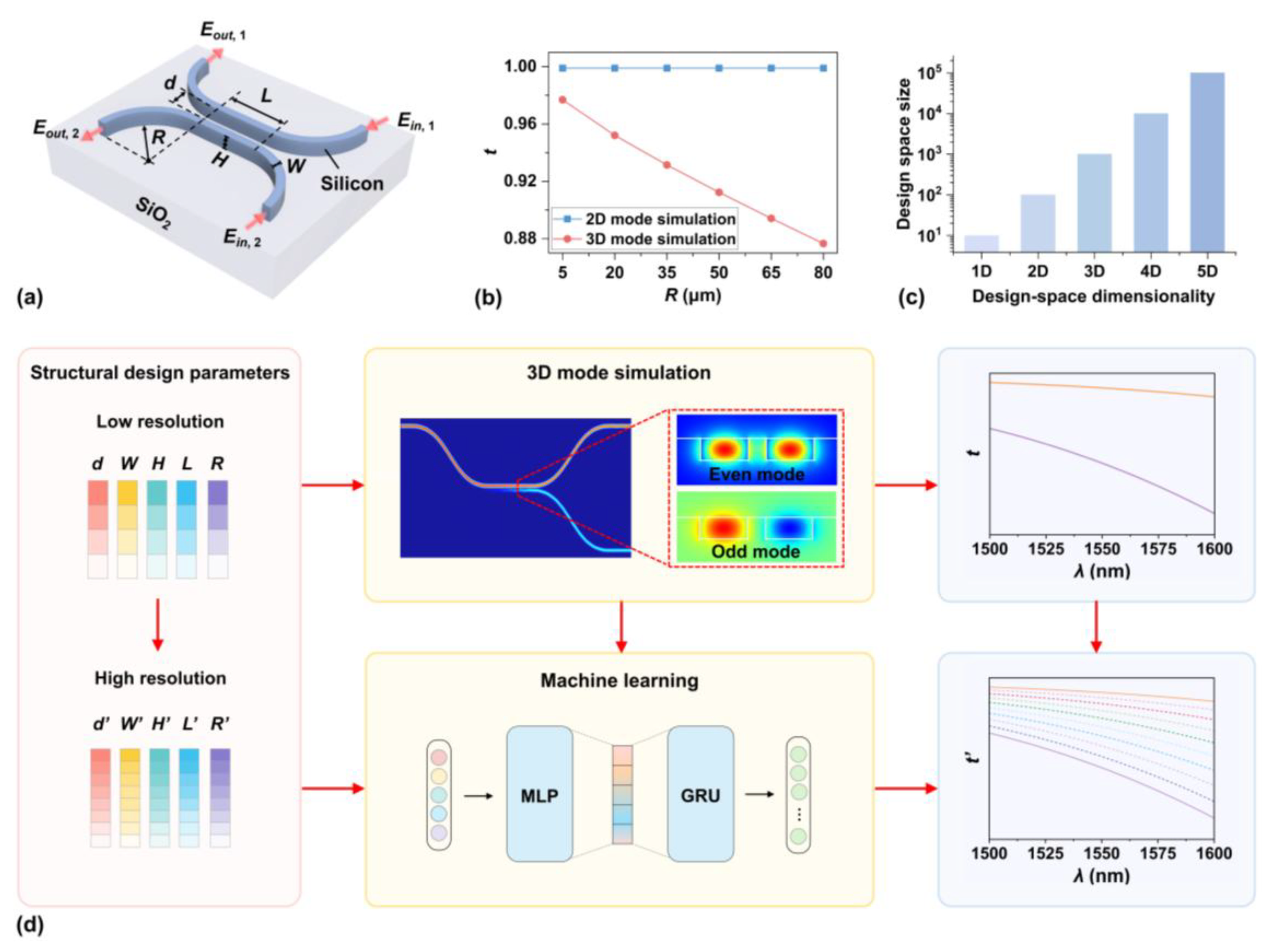
Figure 2.
(a) Top-view device schematic of a Type-I DC, showing the in-plane SDPs (d, L, R). (b) Comparison of t’ versus λ obtained from 3D finite-difference time-domain (FDTD) simulations and ML-based method for six test samples (TSs). (c) Comparison between 3D-FDTD-calculated t and ML-predicted t’. Each dot represents one data point, and the red solid line indicates the diagonal reference. (d) Error distribution corresponding to the data points in (c). (e) Mean squared error (MSE) and coefficient of determination (R2) for the training, validation and test datasets. (f) Shapley additive explanations (SHAP) analysis showing the contributions of d, W, H, L, and R to the predictions of t’(λ). (g) MSE and (h) R2 for training datasets Nos. 1 – 6 in Table I.
Figure 2.
(a) Top-view device schematic of a Type-I DC, showing the in-plane SDPs (d, L, R). (b) Comparison of t’ versus λ obtained from 3D finite-difference time-domain (FDTD) simulations and ML-based method for six test samples (TSs). (c) Comparison between 3D-FDTD-calculated t and ML-predicted t’. Each dot represents one data point, and the red solid line indicates the diagonal reference. (d) Error distribution corresponding to the data points in (c). (e) Mean squared error (MSE) and coefficient of determination (R2) for the training, validation and test datasets. (f) Shapley additive explanations (SHAP) analysis showing the contributions of d, W, H, L, and R to the predictions of t’(λ). (g) MSE and (h) R2 for training datasets Nos. 1 – 6 in Table I.
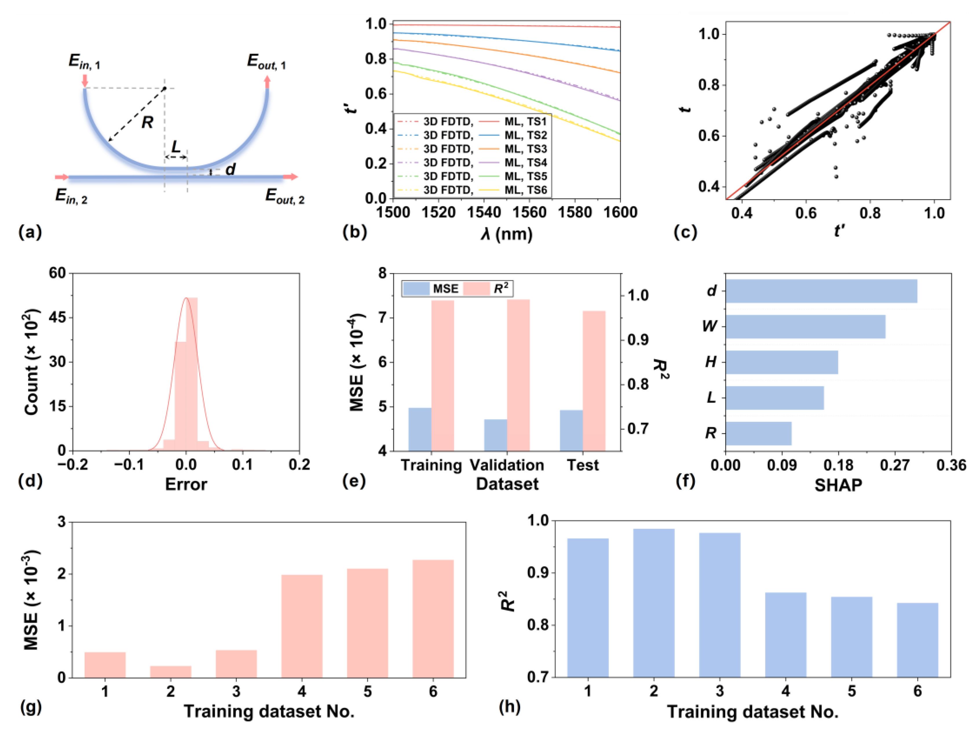
Figure 3.
(a) Top-view device schematic of a Type-II DC, showing the in-plane SDPs (d, L, R). (b) Comparison of t’ versus λ obtained from 3D FDTD simulations and ML-based method for six TSs. (c) Comparison between the 3D-FDTD-calculated t and ML-predicted t’. Each dot represents one data point, and the red solid line indicates the diagonal reference. (d) Error distribution corresponding to the data points in (c). (e) MSE and R2 for the training, validation and test datasets. (f) SHAP analysis showing the contributions of d, W, H, L, and R. (g) MSE and (h) R2 for training datasets Nos. 7 – 12 in Table II.
Figure 3.
(a) Top-view device schematic of a Type-II DC, showing the in-plane SDPs (d, L, R). (b) Comparison of t’ versus λ obtained from 3D FDTD simulations and ML-based method for six TSs. (c) Comparison between the 3D-FDTD-calculated t and ML-predicted t’. Each dot represents one data point, and the red solid line indicates the diagonal reference. (d) Error distribution corresponding to the data points in (c). (e) MSE and R2 for the training, validation and test datasets. (f) SHAP analysis showing the contributions of d, W, H, L, and R. (g) MSE and (h) R2 for training datasets Nos. 7 – 12 in Table II.
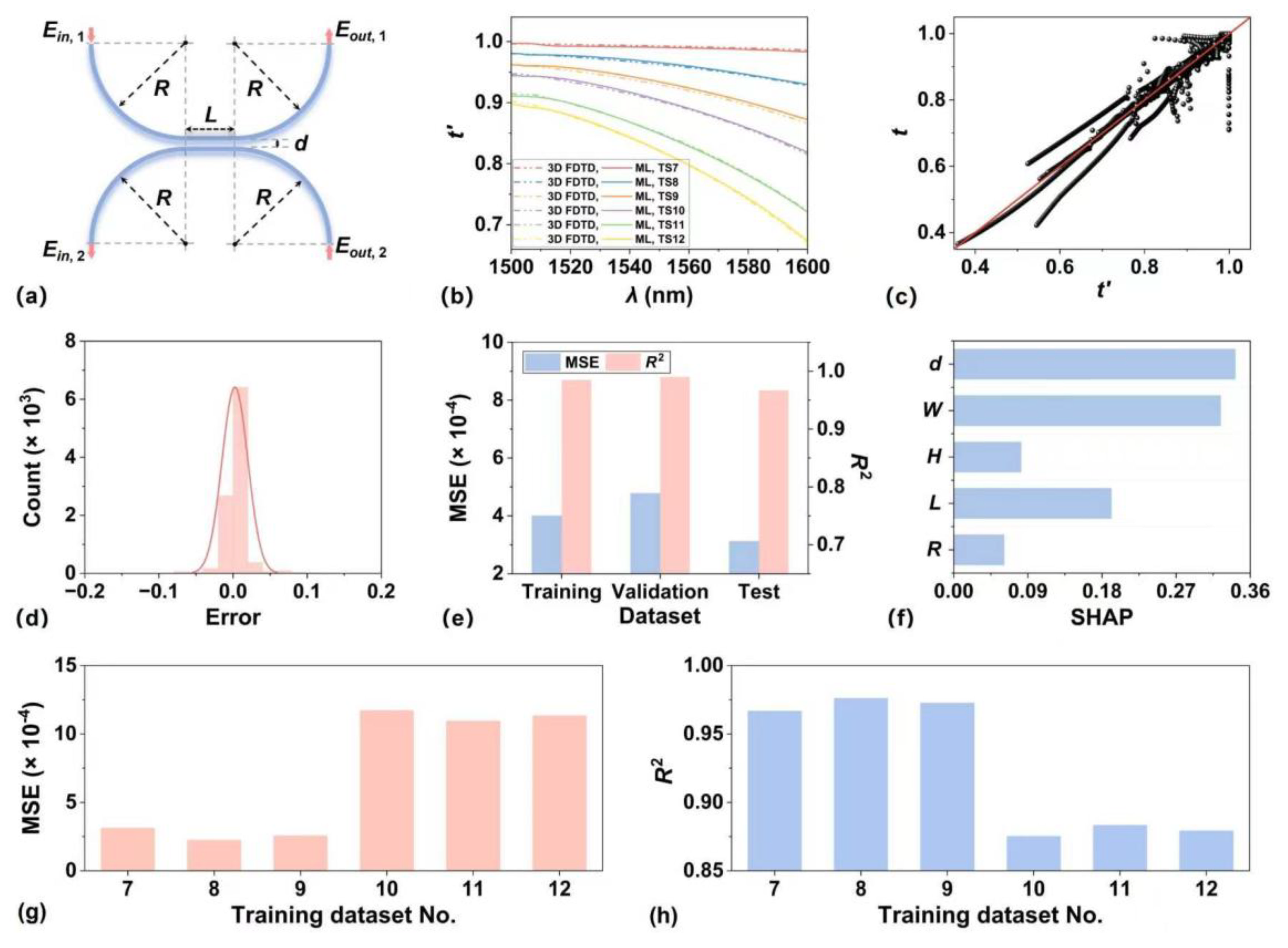
Figure 4.
(a) Comparison of computing times for a single SDP vector of Type-I DCs with different bending radii R, obtained using the ML-based method and 3D FDTD simulations with mesh-accuracy (MA) settings of MA = 1 and MA = 5. (b) Top-view schematic of a DC under the two 3D FDTD simulation settings compared in (a). The right insets show the corresponding zoom-in views. (c) Overall computing time of the ML-based method versus test dataset size.
Figure 4.
(a) Comparison of computing times for a single SDP vector of Type-I DCs with different bending radii R, obtained using the ML-based method and 3D FDTD simulations with mesh-accuracy (MA) settings of MA = 1 and MA = 5. (b) Top-view schematic of a DC under the two 3D FDTD simulation settings compared in (a). The right insets show the corresponding zoom-in views. (c) Overall computing time of the ML-based method versus test dataset size.
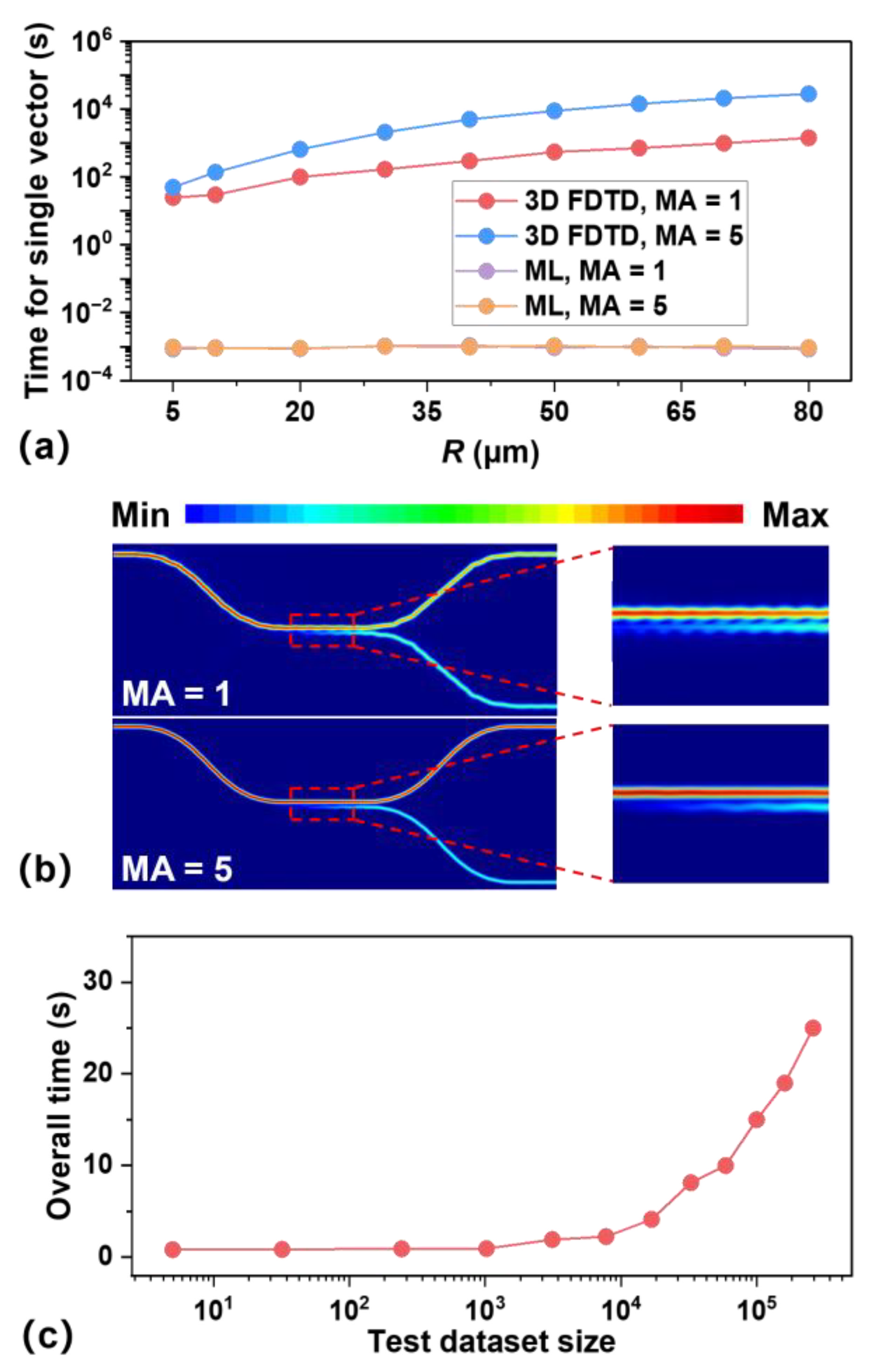
Figure 5.
(a), (b) Comparison of t’ versus λ obtained from 3D FDTD simulations and the ML-based method for three inverse-design examples (IDEs) of Type-I and Type-II DCs, respectively, with d, L, R treated as design variables and fixed W and H. (c), (d) Corresponding results with d, W, L, R treated as design variables and fixed H. In (a), (b), W = 400 nm. In (a) – (d), H = 220 nm.
Figure 5.
(a), (b) Comparison of t’ versus λ obtained from 3D FDTD simulations and the ML-based method for three inverse-design examples (IDEs) of Type-I and Type-II DCs, respectively, with d, L, R treated as design variables and fixed W and H. (c), (d) Corresponding results with d, W, L, R treated as design variables and fixed H. In (a), (b), W = 400 nm. In (a) – (d), H = 220 nm.
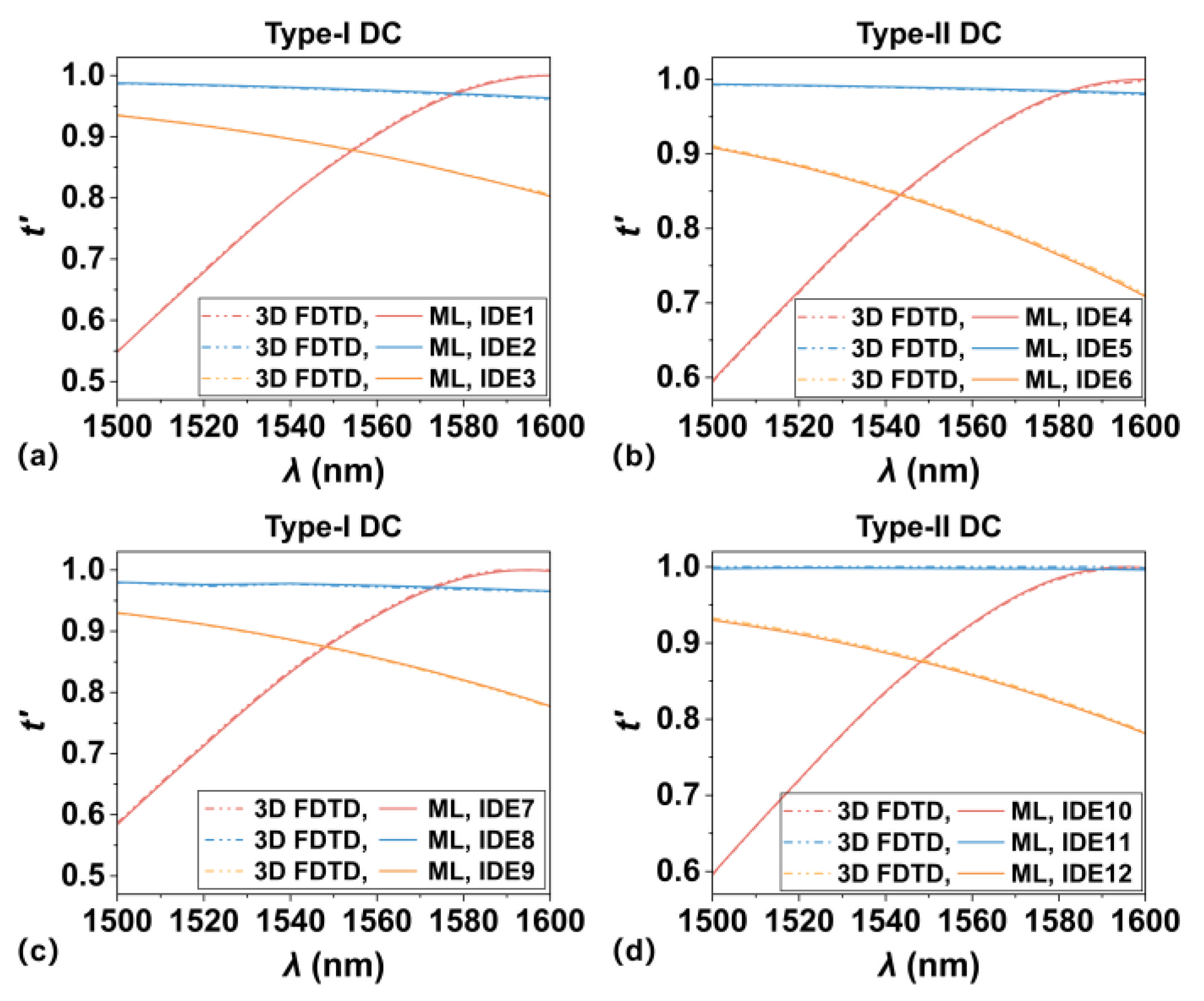
Figure 6.
(a) Microscopic images of the fabricated Type-I and Type-II DCs. (b) Comparison of experimental (Exp.) and ML-framework-predicted t versus λ with varying (i) d, (ii) W, (iii) L, (iv) R for Type-I DCs. (c) Corresponding results for Type-II DCs. In (b) and (c), λ ranges from 1535 nm to 1565 nm. In (i), W = 500 nm, H = 220 nm, L = 3 μm, R = 20 μm. In (ii), d = 200 nm, H = 220 nm, L = 3 μm, R = 20 μm. In (iii), d = 200 nm, W = 500 nm, H = 220 nm, R = 20 μm. In (iv), d = 200 nm, W = 500 nm, H = 220 nm, L = 3 μm.
Figure 6.
(a) Microscopic images of the fabricated Type-I and Type-II DCs. (b) Comparison of experimental (Exp.) and ML-framework-predicted t versus λ with varying (i) d, (ii) W, (iii) L, (iv) R for Type-I DCs. (c) Corresponding results for Type-II DCs. In (b) and (c), λ ranges from 1535 nm to 1565 nm. In (i), W = 500 nm, H = 220 nm, L = 3 μm, R = 20 μm. In (ii), d = 200 nm, H = 220 nm, L = 3 μm, R = 20 μm. In (iii), d = 200 nm, W = 500 nm, H = 220 nm, R = 20 μm. In (iv), d = 200 nm, W = 500 nm, H = 220 nm, L = 3 μm.
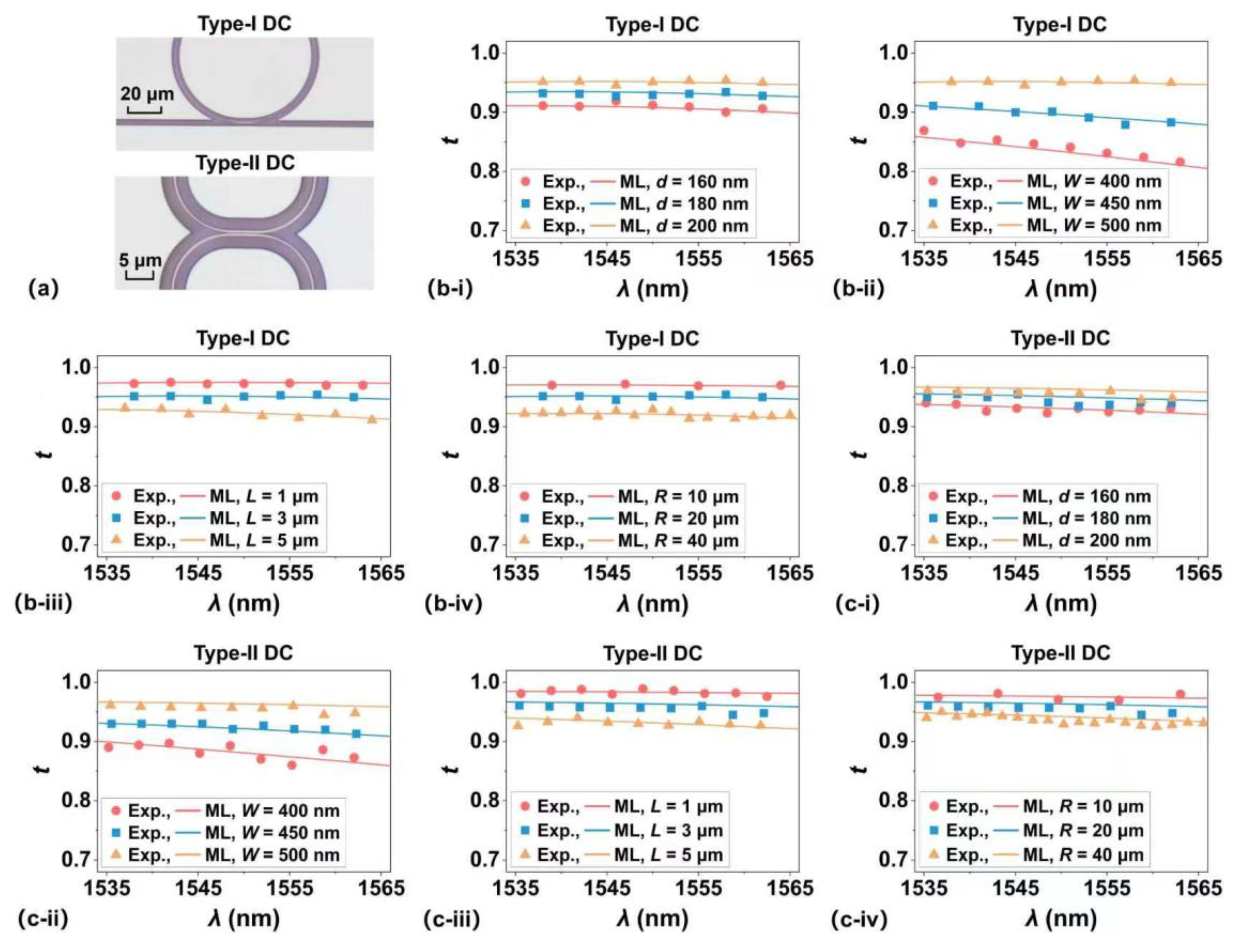
Figure 7.
(a), (b) Comparison of experimentally (Exp.) extracted and ML-predicted t versus λ for three inverse-design examples (IDEs) of Type-I and Type-II DCs, respectively, with d, L, R treated as design variables and fixed W and H. W = 400 nm and H = 220 nm.
Figure 7.
(a), (b) Comparison of experimentally (Exp.) extracted and ML-predicted t versus λ for three inverse-design examples (IDEs) of Type-I and Type-II DCs, respectively, with d, L, R treated as design variables and fixed W and H. W = 400 nm and H = 220 nm.
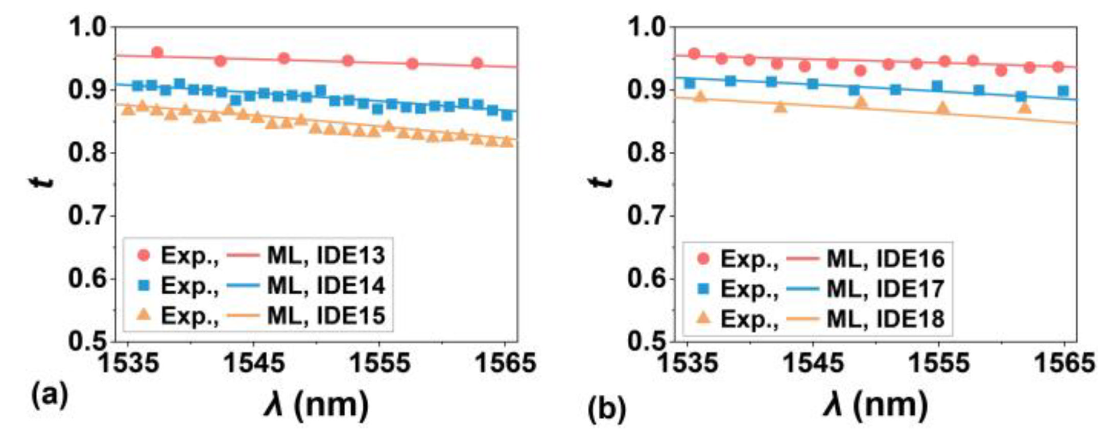
Disclaimer/Publisher’s Note: The statements, opinions and data contained in all publications are solely those of the individual author(s) and contributor(s) and not of MDPI and/or the editor(s). MDPI and/or the editor(s) disclaim responsibility for any injury to people or property resulting from any ideas, methods, instructions or products referred to in the content. |
© 2026 by the authors. Licensee MDPI, Basel, Switzerland. This article is an open access article distributed under the terms and conditions of the Creative Commons Attribution (CC BY) license (http://creativecommons.org/licenses/by/4.0/).
Copyright: This open access article is published under a Creative Commons CC BY 4.0 license, which permit the free download, distribution, and reuse, provided that the author and preprint are cited in any reuse.


