

Submitted:
20 June 2026
Posted:
22 June 2026
You are already at the latest version
Abstract
Silver (Ag)-based conductive coatings are widely used in electrical contacts due to their excellent electrical conductivity, low contact resistance, good thermal stability and oxidation resistance, although their susceptibility to sulfidation and environmental corrosion is a concern under certain service conditions. In recent years, significant progress has been achieved in both the manufacture and performance optimization of Ag-based coatings to satisfy the demanding requirements of modern electrical and electronic systems. This review summarizes recent advances in fabrication techniques and processing parameters for Ag-based coatings, including electroplating, electroless deposition, magnetron sputtering, electrospark deposition, thermal spraying, and electrical explosion spraying on metallic substrates, particularly on copper and steel substrates. More attention is given to microstructural design strategies, such as the incorporation and homogeneous dispersion of reinforcement or solid lubricant phases within the Ag matrix, to enhance contact reliability and operational endurance. The performance of Ag-based coatings is analyzed in terms of their physical, chemical and mechanical properties, electrical contact resistance, friction and wear behavior, arc erosion resistance, and environmental durability under different service conditions. Key challenges, including coating degradation under high electrical loads, mechanical wear, and corrosive environments, are highlighted. Future research directions are outlined, focusing on multifunctional coating structures that enhance surface performance and ensure the long-term durability of electrical contacts.
Keywords:
silver coatings
; thin films
; copper substrates
; deposition techniques
; surface engineering
; surface characteristics
; friction
; wear
; corrosion
; erosion
; electrical contacts
1. Introduction
Electrical contact materials (ECMs) are conductive materials widely used as critical components in electrical and electronic systems [1,2,3,4]. The performance, reliability, and service life of electrical contacts are strongly determined by the electrical and thermal conductivity, hardness, mechanical strength, wear resistance, oxidation resistance, corrosion resistance, as well as the chemical and thermal stability of ECMs [1,5,6].
Electrified tribological contacts are subjected to complex damage mechanisms [7]. Consequently, ECMs must operate reliably under current-carrying friction (CCF), combining high electrical and thermal conductivity, low and stable electrical contact resistance (ECR), high wear resistance, and strong resistance to arc welding [2,8,9]. During CCF, localized thermal effects from Joule heating and electrical arcing can promote the formation of non-conductive oxide layers or lubricating films arising from wear debris and solid additives used in sliding electrical contacts (SECs) [2,10]. These phenomena alter the electrical, mechanical, and tribological properties of ECMs, increasing ECR, accelerating wear and material transfer, and degrading the contact interface [7,10,11,12]. Cumulatively, these factors can lead to intermittent or severe contact failures, reduced service life, and potential short circuits, representing a major challenge for practical applications and motivating continued research into innovative strategies for developing reliable and durable ECMs for bulk and coated electrical contacts operating under harsh service conditions.
Strategies to mitigate contact failures resulting from thermal stresses and mechanical, and electrical wear focus on controlling the underlying damage mechanisms. These approaches include the proper selection and optimization of ECMs to suppress wear and electrical degradation, structural design modifications to reduce stress concentration and thermal accumulation, the implementation of advanced manufacturing techniques to tailor microstructure and phase distribution, and surface and interface engineering to stabilize the contact interface and limit oxidation and material transfer. Furthermore, optimization of contact conditions between the mating frictional bodies is employed to control contact temperature, current distribution, and frictional behavior [2,9,13].
Copper (Cu)- and silver (Ag)-based materials are the most employed ECMs in industrial and domestic applications [1,2,3]. Pure Cu and Ag are soft, malleable, and ductile metals that exhibit excellent electrical and thermal conductivity but relatively low wear resistance [1,2]. Pure Cu is susceptible to oxidation and yields comparatively low mechanical strength, although it exhibits slightly higher mechanical durability than pure Ag. In contrast, pure Ag provides superior resistance to oxidation but is more expensive than Cu [1,14,15]. The formation of non-conductive oxide layers on Cu surfaces reduces conductivity, degrading service performance and contact reliability [3,14].
A conventional ECM design widely used in electrical and electronic systems consists of a Cu substrate coated with a thin Ag surface layer, combining the high conductivity and corrosion resistance of Ag with the mechanical strength and cost-effectiveness of the Cu substrate [3]. Ag-based composite coatings deposited on metallic substrates have been shown to mitigate abnormal heat generation at contact interfaces during operation due to their high electrical conductivity, low coefficient of friction (COF), formation of protective tribofilms, and high atomic diffusion rate [15,16]. However, the low hardness of Ag coatings accelerates wear, which may lead to premature exposure of the underlying metallic substrate [3,17]. In atmospheric conditions, Ag/Cu contacts can experience micro-galvanic coupling between the Ag coating and the Cu substrate, with Cu acting as the anode, which accelerates Cu dissolution and material degradation [3]. Elevated relative humidity further promotes thin electrolyte films and corrosion products on the surface, increasing ECR and localized thermal damage during switching operations [3,18].
Approaches to enhance the properties and service performance of pure Ag coatings electroplated on copper or other metallic substrates primarily involve the development of Ag-based composite coatings and their deposition using advanced techniques.
Ag-based composite coatings typically consist of an Ag metallic matrix reinforced with secondary or ternary phases, including metallic elements such as tungsten (W), antimony (Sb), nickel (Ni), tin (Sn), aluminum (Al), and related alloys [3,13,19,20,21,22,23,24], as well as carbonic materials such as graphite, graphene), carbon nanotubes (CNTs) and carbon black [8,25,26,27,28,29,30]. Additionally, hybrid coatings have been developed based on multiphase systems incorporating Ag with other functional components, such as Ag-Ni-N, Ni-C-Ag-N, MoN-Ag, Ag-CuO, Ag-CdO, Ag-SnO2, Ag-ZnO, and Ag-TiB2 systems [31,32,33,34,35,36,37,38,39,40,41,42].
Over the past decades, a wide range of deposition techniques have been employed to fabricate Ag-based composite and hybrid coatings, including electroplating [43,44,45,46], electroless deposition [21,22,47], magnetron sputtering [17,20,33], electrospark deposition (ESD) [48,49,50,51,52], thermal spraying [25,53,54,55], and electrical explosion spraying [31,32,34,40,41,42]. Although the incorporation of minority phases into the Ag matrix, or surface modifications can enhance the mechanical and tribological performance of Ag-based coatings, these approaches may affect electrical conductivity and increase contact resistance. Therefore, optimizing the balance between electrical, mechanical, and tribological properties is essential for achieving synergistic performance in ECMs [8]. Moreover, each deposition technique presents both advantages and limitations (e.g., coating thickness control, microstructural uniformity, interfacial bonding, process complexity, scalability) [41,56,57,58,59,60].
Despite substantial progress in ECM design and manufacturing, many factors still influence the development of high-performance and durable Ag-based conductive coatings that meet stringent operational and safety requirements in domestic and industrial applications [2,3,8]. In particular, the complex relationships among starting materials, ECM composition, deposition techniques, resulting microstructure, functional properties, and dominant failure mechanisms at Ag-based composite coating and contact interfaces are insufficiently understood and require further investigation.
Although extensive research on Ag-based coatings has been reported, comprehensive reviews that examine the interdependence among coating composition, deposition methods, and performance under diverse operational and environmental conditions are still limited. This review addresses this gap by summarizing recent advances in the design and performance of Ag-based composite coatings, with emphasis on the influence of fabrication techniques and processing parameters. Greater focus is given to coatings deposited on Cu and steel substrates, using techniques such as electroplating, electroless deposition, magnetron sputtering, electrospark deposition, thermal spraying, and electrical explosion spraying. This review also highlights microstructural engineering strategies, including the incorporation and uniform distribution of reinforcements (e.g., transition metals, metal oxides) and carbon-based solid lubricants within the Ag matrix, to enhance contact reliability and service life. The underlying mechanisms determining electrical, mechanical, tribological, and corrosion behavior under various conditions are discussed, where applicable. In addition, future research directions are proposed, focusing on multifunctional coating designs to improve surface performance and ensure long-term durability of electrical contacts. By synthesizing current findings, this review provides useful guidance for researchers and industry practitioners developing electrical contacts.
2. Methodology
This article presents a narrative review based on a structured literature search of publications from 2000 to February 2026 in Scopus and Web of Science, focusing on recent and relevant studies concerning the manufacture, microstructure, and functional performance of Ag-based conductive coatings for electrical contact applications.
Greater emphasis was placed on studies published during the last 10 years to present the most recent developments in this field. The search strategy focused on three main aspects: Ag-based coatings, deposition technologies, and performance under electrical contact conditions. The following keyword combination was used: (“silver coating” OR “Ag coating” OR “silver composite coating” OR “Ag-based composite coating”) AND (“electrodeposition” OR “electroless deposition” OR “magnetron sputtering” OR “PVD” OR “electrospark deposition” OR “thermal spraying” OR “cold spray” OR “electroexplosive spraying”) AND (“electrical contact” OR “electrical contact resistance” OR “arc erosion” OR “tribology” OR “friction” OR “wear” OR “corrosion”).
The initial search identified 172 records in Web of Science and 191 records in Scopus. After applying the initial selection criteria, limited to English-language publications and excluding early access documents, 168 records remained in Web of Science and 170 records in Scopus. Duplicate records were removed using EndNote 2025, version 25.3.1, resulting in 203 records for title and abstract screening. At this stage, 41 papers were excluded because they were outside the scope of the review. The remaining 167 full-text reports were assessed in detail. Of these, 12 were excluded because they focused on biomedical, antimicrobial, or biological applications of Ag-based coatings. Finally, 156 studies met the inclusion criteria and were considered in the qualitative synthesis.
Studies were selected when they addressed Ag-based coatings, Ag-based composite coatings, or Ag-containing thin films with relevance to electrical contact applications. Eligible studies also had to report information on at least one of the following aspects: coating fabrication, microstructure, electrical performance, tribological behavior, wear resistance, arc erosion resistance, corrosion resistance, or environmental durability. Studies were excluded when their focus was limited to biomedical, antimicrobial, or biological applications, or when the coating system was not relevant to electrical contacts.
The selected studies were analyzed qualitatively and organized according to deposition method, coating composition, substrate type, microstructural features, and reported functional performance. No quantitative synthesis was performed, as the reviewed studies differed substantially in terms of materials, deposition conditions, testing protocols, and reported performance indicators.
The annual distribution of publications (Figure 1) indicates steady and sustained growth in research on Ag-based coatings for electrical contact applications. While relatively limited activity was observed in the early 2000s, a gradual increase is evident after 2010, followed by a marked expansion from 2017 onward. The most significant rise occurred between 2021 and 2025, with 2025 representing the peak in publication output in both Scopus and Web of Science.
The keyword co-occurrence network (Figure 2) reveals a well-structured and interconnected research landscape centered on Ag-based coatings. The term silver appears as the dominant node, positioned at the core of the map, highlighting its central role across multiple research directions. Four main thematic clusters can be distinguished. The red cluster is primarily associated with corrosion-related research, including terms such as corrosion resistance, electrodeposition, electroplating, and electrochemical corrosion. This indicates a strong emphasis on protective coatings and durability enhancement. The green cluster focuses on tribological performance, with keywords such as tribology, friction, wear resistance, and composite coatings, reflecting increasing interest in improving mechanical and functional behavior under service conditions. The blue cluster groups terms related to thin films and structural characterization, including thin films, hardness, and X-ray diffraction analysis, suggesting a materials engineering perspective centered on microstructural optimization. Finally, the yellow central cluster links coatings, magnetron sputtering, and surface behavior, acting as a bridge between deposition techniques and performance outcomes. The network illustrates a multidisciplinary convergence between corrosion science, tribology, surface engineering, and advanced deposition technologies. It shows that current research on Ag-based coatings is not isolated within a single domain, as it integrates processing methods, structural characterization, and functional performance into a coherent and evolving research field.
3. Ag-Based Coatings Produced by Electrodeposition
3.1. Overview of Electrodeposition for Ag-Based Coatings
Electrodeposition techniques can be classified by deposition mechanism into electrochemical methods (electroplating, electrophoretic coating) and chemical methods (electroless deposition, immersion plating) [61]. Electrochemical deposition uses an external power source, whereas chemical deposition does not require an external power source.
Electroplating is a versatile and widely used technique to fabricate metal coatings such as pure and composite Ag-based coatings. In Ag matrix composite (AgMC) coatings, Ag and reinforcement particles are codeposited on a conductive substrate by electrochemical deposition using an external power source. This method allows precise control of layer thickness and microstructure, enables high incorporation of nanoparticles, and is scalable for industrial applications. Limitations include the need for proper bath maintenance and potential non-uniform deposition on complex substrates.
A conventional electroplating system consists of four essential components, such as a positive electrode (anode), a negative electrode (cathode), an electrolytic solution, and a power supply [62]. The configuration of these components may vary according to the specific application requirements [62]. An electroplating system with a silver plate anode and a copper plate cathode, used for the electrodeposition of an Ag-graphene coating on a Cu substrate, is illustrated in Figure 3 [44].
The electroplating process involves surface preparation and cleaning of the cathode, application of a conductive layer if necessary, immersion of the cathode in the electrolytic solution, and passage of an electric current through the electrochemical cell to deposit metal on the cathode surface, which constitutes the fundamental principle of electroplating. Electrolyte composition is critical, as the type of metallic ions directly affects coating quality, including composition, thickness, adhesion, and surface morphology.
Typical electrolyte components, selected examples [21,23,45,63], and their influence in the electrodeposition of Ag-based coatings are presented in Figure 4.
The overall deposition rate and the amount of metal deposited are determined by the current flowing between the anode and cathode, in accordance with Faraday’s law of electrolysis, as expressed in Equations (1) and (2) [61,62]:
where Q is the total electric charge transferred during deposition (C), z is the number of electrons involved in the electrode reaction, m is the number of moles deposited, F is Faraday’s constant (96,485 C/mol), x is the deposit thickness (cm), t is the deposition time (s), ϕ is the current efficiency for metal deposition (ϕ ≤ 1), j is the current density (A/cm2), M is the molar mass of the deposited metal (g/mol), and ρ is the deposit density (g/cm3).
Q = z·m·F
The electrodeposition of metal matrix composite (MMC) coatings through the incorporation of insoluble particles dispersed in a plating bath into a growing metal layer is comprehensively reviewed by Walsh et al. [61,64]. These works describe the fundamental principles of composite plating, including the underlying mechanisms and mathematical models, and provide insights into the formation of uniform, high-quality MMC coatings. The key processes involved include particle convection toward the cathode surface, mechanical entrapment within the growing metal matrix, and electrophoretic migration to the growing metal deposited on the cathode surface [61,64]. The properties of MMC coatings are controlled by multiple interrelated factors, including characteristics of particles, electrolyte, electrode, and tank, as well as operating conditions [45,61,64] (Figure 5).
Additional factors include electroplating cell design and configurations such as rotating disk or cylinder electrodes, plate-in-tanks, or parallel plate electrodes. Mathematical models incorporate variables related to the electrolyte, electrodes, and reinforcing particles, as well as electrochemical reactions, charge-transfer and kinetic processes, and mass transport, to predict coating composition and the resulting physical, mechanical, and electrical properties of deposited MMC coatings [61,64].
3.2. Selected Examples of Electrodeposited Ag-Based Composite Coatings Using Ag and Other Metal Salts
Selected examples of electrodeposited Ag-based composite coatings using Ag and other metal salts are presented in Table 1.
Kola et al. [45] reported the electrodeposition of Ag-W coatings on Cu rotating cylinder electrodes (RCEs) from a non-cyanide, acidic thiourea-citrate-AgSO4-Na2WO4 electrolyte (Table 1). Tungsten (W) was incorporated by induced codeposition with Ag, where Ag+ ion reduction was mass-transport controlled and W6+ ion reduction was kinetically controlled and influenced by thiourea. The RCE configuration enabled precise mass-transport control, and a low Ag+/tungstate ion ratio further promoted W incorporation. XRF and EDS analyses showed that W content increased with both tungstate concentration and applied current density. A maximum W content of 18 wt.% was achieved at 150 mM tungstate and 320 mA/cm2, substantially exceeding previously reported values for Ag-W electrodeposits (~5 wt.% W) [21,22]. SEM-EDS analysis detected S (from thiourea) and O (attributed to WO3 formation) in addition to Ag and W in the deposits. The surface morphology strongly depended on deposition conditions. At 5 mA/cm2, rough, plate-like structures formed in 30–75 mM tungstate baths, while smooth, nodular morphologies were obtained at 150 mM tungstate. At 320 mA/cm2, dendritic deposits developed from 30–150 mM tungstate. This trend aligns with induced codeposition behavior, where higher current densities and tungstate concentrations promote growth instabilities and dendrite formation, while lower currents favor compact morphologies. Although this study [45] provides mechanistic insight into induced codeposition, the electrical, mechanical, tribological, and electrochemical properties of the Ag-W coatings were not evaluated.
In another study, Zhu et al. [23] prepared Ag-Sb coatings with 0–2.72 wt.% Sb by a non-cyanide electrodeposition process (Table 1) using a three electrode cell with Ag anode, Cu working electrode, and Ag/AgCl reference electrode, and an anode-to-cathode distance of 4 cm. The addition of KSbOC4H4O6 (brightener) and NaKC4H4O6 (brightener/stabilizer) to the Ag plating bath enabled the incorporation of 0.8–2.72 wt.% Sb and resulted in a flatter, denser morphology and uniform Sb distribution within the Ag matrix, compared with the additive-free Ag coating (Ag-0Sb). Although the coating thicknesses varied slightly (5.27–5.83 μm), Sb content strongly influenced the coating performance. Vickers hardness increased with Sb addition up to 2 wt.% (146.5 HV) and decreased at 2.72 wt.% Sb due to increased internal stress and defect formation. Resistivity increased with Sb content because of solid-solution strengthening and enhanced electron scattering. However, the resistivity of Ag-2Sb coating (1.66 × 10⁻⁷ Ω·m) remained acceptable for electrical contacts. Among all coatings, Ag-2Sb exhibited the best performance, showing the highest hardness (146.5 HV), lowest COF (0.56), lowest wear rate (0.84 × 10⁻⁶ mm3/(N⋅m)), and highest corrosion resistance in 3.5 wt.% NaCl solution, with a corrosion current density of 4.2 × 10⁻⁷ A/cm2, and a corrosion rate of 1.41 × 10⁻² mm/year. Compared with pure Ag coating, the Ag-2Sb coating exhibited a 61.3% increase in hardness, a 29.1% reduction in COF, a tenfold decrease in wear rate, and a 27.3-fold reduction in corrosion rate, highlighting its potential for electrical contact applications in harsh environments.
3.3. Selected Examples of Electrodeposited Ag-Based Composite Coatings by Incorporation of Insoluble Particles in the Ag Plating Baths
Selected examples of electrodeposited Ag-based composite coatings by incorporation of insoluble particles in the Ag plating baths are summarized in Table 2.
Cosmuş et al. [65] investigated the effect of insoluble TiB2 NPs (0.5–4 g/L) in the Ag electroplating bath on the microstructure, hardness, corrosion resistance, and electrical performance of DC electrodeposited Ag-TiB2 coatings on Cu substrates. Compared with pure Ag coatings produced under similar conditions, TiB2 NP reinforcement promoted grain refinement through surface-induced nucleation and growth restriction, higher hardness (79.5–82.2 HV vs. 74.1 HV), and slightly increased electrical resistivity (0.280–0.294 Ω vs. 0.278 Ω) due to enhanced electron scattering at the TiB2 NP - Ag matrix interfaces. The coatings also showed improved corrosion resistance in 3.5 wt.% NaCl solution and enhanced functional performance. Both pure and composite Ag-based coatings exhibited superior arc erosion resistance and significantly longer service life (10,000 switching cycles at 4 kW, 220 V AC, with 2 s on/off intervals) compared with bare Cu substrates, which failed after 1,139 cycles. The properties and performance of the Ag-based coated Cu contacts were strongly influenced by the TiB2 NP content, dispersion, and surface integrity. The best-performing composite coatings were obtained from an Ag plating bath containing 1 g/L TiB2 NPs, while higher TiB2 NP contents (2–4 g/L) caused NP agglomeration, increased surface roughness, and reduced corrosion and service durability. The optimized 74.6 μm-thick Ag-TiB2-coated Cu contacts (Figure 6) show strong potential as substitutes for toxic Ag-CdO-coated Cu contacts in electrical switching applications. However, conventional DC electrodeposition relies on toxic potassium cyanide (KCN) as the Ag complexing agent, necessitating strict safety and chemical management protocols. Consequently, current research is increasingly focused on cyanide-free electrodeposition routes.
In the study by Arai et al. [63], a viable cyanide-free electroplating for Ag/CNT coatings on an Ag strike layer/Cu substrate using an eco-friendly iodide bath was reported. The effects of AgI-KI bath pH (1, 9, and 12) and MWCNT content (0–10 g/L) were thoroughly investigated, revealing the strong pH dependence of bath stability. At pH 12, stable Ag-iodide complexes formed, yielding a solution stable for 30 days under ambient conditions with 100% current efficiency. CNT incorporation in the composite coatings increased with CNT content, reaching 1.5 vol.% CNTs at 10 g/L. Aeration enabled uniform CNT dispersion without surfactants or dispersants. Compared with pure Ag coating deposited under identical conditions without CNTs, the Ag-1.2 vol.% CNT coating exhibited higher hardness (63.2 HV vs. 60.4 HV) and a lower COF (0.4–0.5 vs. 0.6), with only a slight increase in resistivity (1.9 μΩ·cm vs. 1.8 μΩ·cm) [63]. The friction reduction was attributed to the solid-lubricant effect of CNTs within the wear tracks. The authors [63] proposed this iodide-based process as a viable alternative for electrical connector fabrication. However, key parameters such as the thicknesses of the Ag/CNT and pure Ag top layers, the Ag strike layer, substrate surface preparation, and coating roughness, were not specified.
Sun et al. [44] developed a cyanide-free electrodeposition approach to fabricate high-quality Ag-graphene (Ag-G) coatings on Cu substrates (Figure 3) for electrical contact applications. The electrolyte contained nicotinic acid (niacin) as a green complexing agent, silver nitrate (AgNO3) as the Ag source, 0.5 g/L graphene, C12H25SO4Na, and C12H25SO3Na as surfactants, and PEG 400 as a leveler (Table 2). A pure Ag coating was deposited under the same conditions in the nicotinic acid electrolyte without graphene and additives. This study [44] proposed an effective materials design strategy in which the pyridine ring of nicotinic acid interacts with graphene through π-π stacking, thereby promoting uniform dispersion of graphene within the Ag matrix and suppressing its agglomeration in the electrolyte. The corresponding electrodeposition mechanism is schematically illustrated in Figure 7 [44].
SEM, EDS, AFM, Raman imaging (Figure 8), and 3D white-light interferometry revealed that the Ag-G coating from the nicotinic acid bath exhibited higher graphene incorporation and more uniform dispersion (13.75 wt.% C in longitudinal section, 4.6 wt.% C in cross-section) with a denser, smoother morphology than that from the sodium thiosulfate (Na2S2O3) bath (5.79 wt.% C in longitudinal section, 1.5 wt.% C in cross-section), which showed heterogeneous distribution and a rougher surface [44]. Accordingly, surface roughness (Ra) increased from 0.15 μm (pure Ag coating) to 0.3 μm (Ag-G coating from the nicotinic acid bath) and 1.5 μm (Ag-G coating from the thiosulfate bath) [44]. The absence of π-π interactions in the thiosulfate system led to poorer graphene dispersion.
Uniform graphene incorporation refined Ag grains and increased dislocation density, leading to enhanced mechanical, tribological, and current-carrying performance [44]. The Ag-G coating from the nicotinic acid bath achieved a Vickers hardness of 120 HV (~41% higher than pure Ag coating, 85 HV), improved wear resistance, and reduced the coefficient of friction by ~10% under dry sliding (0.54 vs. 0.60), owing to the solid-lubricant effect of graphene. During on-off current-carrying tests, Ag-G contacts exhibited reduced surface oxidation and material accumulation at wear edges, extending service life by over 62% relative to pure Ag contacts. Accordingly, this work [44] presents a sustainable and effective strategy for fabricating high-performance Ag-G electrical contact coatings.
Zhang et al. [46] employed a double-pulse (DP) electroplating (EP) strategy using a 5,5-dimethylhydantoin (DMH)-nicotinic acid (NA) pre-Ag plating bath and an Ag/G composite electrolyte containing 0.5–2 g/L graphene (G) to produce high-quality Ag/G coatings. The combined DP deposition and DMH-NA coordination enhanced cathodic polarization, stabilized Ag+ ions in solution, and refined Ag grains, thereby improving coating performance. Concurrent suppression of hydrogen evolution reduced internal stress and mitigated hydrogen embrittlement, and cracking formation. Both DMH and NA ligands coordinated Ag+ ions by carbonyl, amino, and carboxyl groups, decreasing effective Ag+ activity and retarding electrochemical kinetics. π-π interactions from NA’s pyridine ring inhibited graphene agglomeration, promoting uniform graphene dispersion within the Ag matrix, while DP deposition improved graphene in-plane distribution. The pre-Ag layer formed a dense and uniform transition interface on the Cu substrate, suppressing Ag-Cu displacement reactions and enhancing the adhesion and interfacial stability of the Ag/G coatings under electric arc exposure. Consequently, the Ag/G coatings incorporating a pre-Ag layer exhibited ~51% higher bonding strength than Ag/G coatings without pre-Ag plating. The optimized DP deposition strategy enabled the production of uniform, smooth and dense Ag/G coatings on pre-Ag layer/Cu substrates, with properties dependent on graphene concentration. In contrast, DC deposition (2 g/L G) resulted in non-uniform graphene dispersion and local agglomeration within the Ag matrix. Moreover, DP-deposited Ag/G coating (2 g/L G) exhibited superior performance compared with both DC-deposited Ag/G coating (2 g/L G) and pure Ag coating (Table 3) [46].
Despite comparable thicknesses (Table 3) [46], all DP-deposited Ag/G coatings showed longer electrical contact life with stable contact resistance (~10 mΩ). Uniform graphene dispersion formed a homogeneous conductive network, improving electrical performance and reducing localized material loss and arc intensity. The DMH-NA-assisted DP approach proved effective for producing high-performance Ag/G coatings and provided insight into arc erosion and low-current wear mechanisms [46], but further studies are needed to assess long-term stability in switching devices (e.g., connectors, relays).
Similarly, Sun et al. [66] employed either conventional electroplating (EP) or double-pulse electroplating (DPEP) to deposit a 13.8 μm thick Ag coating (#1) and 13.7–16.1 μm thick Ag-graphene (Ag-G) composite coatings (#2–#4) on Cu substrates. To suppress graphene/graphene oxide (G/GO) agglomeration and restacking in the electrolyte during electrodeposition, the process was optimized through zeta potential (ζ) modulation at a G or GO concentration of 0.75 g/L, combined with EP parameter optimization (Figure 9).
Raman spectroscopy [66] confirmed that the DPEP-optimized process reduced the oxygen-containing functional groups in GO, yielding the Ag-G coating (#4) with the lowest graphene defect density (ID/IG = 0.96) compared with Ag-G coatings #2 and #3 (ID/IG = 1.023, and 1.009, respectively). Coating #4 also exhibited the smoothest surface and densest microstructure, with uniformly dispersed graphene within the Ag matrix. Consequently, it achieved the best performance, including the lowest surface roughness Ra (25.5 nm), smallest Ag grain size (19.4 nm), highest hardness (144.1 HV), lowest COF (0.506), minimum wear volume (14.4 × 105 μm3), and lowest ECR (30 mΩ), exceeding pure Ag and the other Ag-G coatings (Ag grain size: 23.3–32.1 nm, hardness: 92–127.2 HV, roughness Ra: 26.1–104.2 nm, COF: 0.596–0.65, wear volume: 25–50.1 × 105 μm3, ECR: 46–92 mΩ). The enhanced arc erosion resistance under CCF conditions was attributed to graphene, which suppressed arc-induced melting, splashing, and oxidation, thereby maintaining lower and more stable ECR values. Improved graphene structural quality in Ag-G coatings reduced friction and wear through the formation of a stable, low-friction, wear-resistant transfer film on the sliding surface. It also enhanced hardness and arc erosion resistance while lowering ECR, thereby extending the service life of the coated electrical contacts.
4. Ag-Based Coatings Produced by Magnetron Sputtering
4.1. Overview of Magnetron Sputtering for Ag-Based Coatings
Magnetron sputtering (MS) is a physical vapor deposition (PVD) technique in which material is ejected from a source (target) by bombardment with ions generated in a plasma (typically Ar or Ar/N2) and subsequently deposited on a substrate. Depending on the electrical conductivity of the target material, the process employs two main types of power supplies: direct current (DC) sputtering for electrically conductive materials (primarily metals and alloys), and radio frequency (RF) sputtering for electrically insulating materials (mainly ceramics). A key advantage common to both approaches is their ability to produce thin films on a wide variety of substrate types [67].
Magnetron sputtering is widely used for the deposition of pure Ag and AgMC films and coatings on metallic substrates due to its ability to produce fine-grained films with fewer defects and improved thickness uniformity [17,20,68,69]. Moreover, Ag coatings deposited by pulsed DC magnetron sputtering typically exhibit superior hardness and high adhesion compared to those produced by conventional methods such as electroplating, resulting in enhanced tribological performance and increased wear resistance [17,70].
Advanced MS techniques such as high power impulse magnetron sputtering (HiPIMS), glancing angle deposition (GLAD), and glancing angle co-deposition (GLACD), have also been employed to produce pure Ag, AgMC and Ag-doped MMC films and coatings on various substrates, providing improved microstructural control and enhanced mechanical and tribological behavior [20,71,72,73]. The properties of MS coatings are determined by a range of technological and structural parameters, including target chemical composition, deposition mode (DC, RF, HiPIMS, GLAD, GLACD), substrate geometry (shape and dimensions), substrate temperature, substrate rotation speed, substrate bias voltage, target to substrate distance, base pressure, working pressure, gas flow rate, sputtering power, sputtering time, plasma characteristics, as well as the resulting microstructure and phase distribution within the coating [20,74,75].
Sputtering techniques provide several advantages for the fabrication of functional coatings, such as precise control over chemical composition, the ability to produce dense and uniform films, good adhesion to the substrate, and versatility in depositing a wide variety of materials. Furthermore, the HiPIMS technique provides a high degree of plasma ionization (70–100%), compared to only 1–5% in the conventional MS techniques, due to the application of high power to the target in short pulses. This results in high-quality, dense, and compact coatings with refined grains, reduced surface roughness, strong adhesion strength, and improved wear resistance [33,76].
The main disadvantages of magnetron sputtering include relatively high energy consumption, increased equipment complexity and cost, and lower deposition rates compared to alternative coating techniques such as thermal spraying, electrical explosion spraying, and electroplating [25,35,36,37,38,39,40,43,44,45,46,53]. Additionally, the MS process may be less efficient for producing thick coatings due to its typically low growth rate. Conventional MS is also limited by differential target poisoning during reactive sputtering, moderate-to-high residual stresses, and poor coating uniformity on complex geometries due to its line-of-sight nature [77,78]. In contrast, advanced MS techniques (e.g., HiPIMS, pulsed DC magnetron sputtering) provide more stable reactive sputtering conditions and improved film coverage on complex-shaped substrates [76]. Although the films produced by GLAD/GLACD exhibit moderate adhesion and low-to-moderate film density with porous, tilted columnar structures, their residual stress is generally low due to their porous structure [20,71]. These techniques also enhance coating uniformity on complex shapes through geometric shadowing and substrate rotation.
For Ag-based coatings, particularly in self-lubricating coatings (e.g., Ag/MoS2, Ag-diamond-like carbon (DLC)) [79,80,81], exposure to elevated temperatures can promote the diffusion of Ag toward the coating surface. This process may induce significant changes in the coating microstructure and properties, leading to both functional benefits (e.g., enhanced lubricity) and potential long-term degradation [17,33].
4.2. Selected Examples of Magnetron Sputtered Ag-Based Coatings
Selected examples of pure and composite Ag-based coatings deposited by magnetron sputtering on different substrate materials are presented in Table 4.
A comparison of pure Ag coatings deposited on GH4169 substrates by low-temperature (LT) pulsed DC magnetron sputtering (MS) and electroplating (EP), before and after 8 h of high temperature (HT) exposure, was conducted by Li et al. [17]. The 3.75 μm thick MS coatings showed a denser, more uniform surface with larger grains (1.92 nm) and fewer defects than 3.89 μm thick EP coatings (0.76 nm). Heat treatment increased surface protrusions in both Ag coatings, but EP coatings developed larger protrusions, higher porosity, and local flaking with pit formation. At RT, MS coatings exhibited superior mechanical properties (~25% higher hardness, ~135 HV vs. ~108 HV, and 1.2× greater adhesion) but higher COF (0.56–0.80) and wear rate (Kv ≅ 0.31–0.44 × 10⁻⁵ mm3/N·m) than EP coatings (COF = 0.41–0.64, Kv ≅ 0.11–0.40 × 10⁻⁵ mm3/N·m). After HT exposure, hardness decreased by 38% (MS coatings) and 50% (EP coatings), while bonding force dropped from 23 N to 16 N (MS coatings) and from 11 N to 7 N (EP coatings). Despite this, MS coatings showed ~20% lower COF and ~96% lower wear rate than EP coatings at maximum load (820.2 MPa). At RT, wear was mainly abrasive in MS coatings and adhesive in EP coatings, while at HT, both mechanisms were present in all coatings. EP coatings also exhibited fatigue wear under various loads at both temperatures. At RT, MS coatings accumulated abrasive debris in the wear tracks, whereas EP coatings exhibited Ag buildup along the track edges. At HT, some debris in MS coatings were crushed and reattached to the substrate, enhancing surface integrity and lubrication, while side buildup intensified in EP coatings. All coatings displayed gradual material recovery. Molecular dynamics simulations indicated that Ag atoms migrated with the counterbody and formed layered aggregates at both temperatures, with stronger interactions at HT promoting greater clustering. Overall, MS deposition enhanced the mechanical and tribological performance of Ag coatings across temperatures, with relevance for aero-engine fasteners and electrical contacts.
Zhao et al. [68] deposited Ag-In-Cux (x = 1, 3, and 5 wt.% Cu, 1 wt.% In, and the balance Ag) films on Al 6061 substrates by magnetron sputtering at RT. This study evaluated the influence of composition and deposition parameters on optical properties and thermal stability after film annealing at 200 °C for 1 h under vacuum at 0.1 Pa. Increasing Cu content reduced the grain size from 13 nm to 9 nm, and at 5 wt.% Cu, suppressed grain growth and agglomeration, resulting in smoother, more uniform films with improved thermal stability, even though with reduced near-infrared (NIR) reflectivity. Raising the sputtering power from 20 W to 40 W and the deposition time from 1 min to 3 min increased the grain size from 13 nm to 18 nm and initially enhanced reflectivity, which declined beyond optimal conditions. The best performance was obtained for films deposited at 30 W for 2 min, yielding a maximum reflectance of 99.86% and a mean reflectance of 96.22% in the 800–2000 nm range. However, all Ag-In-Cux films showed a significant reflectance loss after heat exposure due to agglomeration-induced film discontinuity. Although Ag-In-Cu films were developed for aerospace and military optical applications, these findings are relevant to electrical contact materials.
The deposition of Ag-Cu coatings on Ti6Al4V disk-shaped substrates using a bipolar HiPIMS technique was reported by Hsu et al. [76]. This approach enabled independent control of pulse parameters for Ag and Cu targets without dual HiPIMS sources or auxiliary power supplies (DC, RF, or pulsed). The coating composition and surface chemistry were analyzed by X-ray photoelectron spectroscopy (XPS), while film thickness was measured using field-emission transmission electron microscopy (FE-TEM). The results showed that the Ag-Cu coatings remained metallic, with no bonding between Ag and Cu. Mutual interference during growth induced compressive stress in Ag (111) and tensile stress in Cu (111), resulting in significantly smaller crystallite sizes (1.2–1.8 nm) compared to pure metallic Ag (27.1 nm) and Cu (13.8 nm) coatings, deposited at 50 A and 2.10 nm/s for Ag, and 100 A and 1.55 nm/s for Cu, respectively. The Cu/Ag ratio in the bimetallic coating increased from 1.9 to 4.4, while the crystallite size decreased from 1.8 nm to 1.2 nm as the Cu target peak current increased from 80 A to 200 A, with the Ag current held at 50 A. Concurrently, the deposition rate declined from 0.76 nm/s to 0.62 nm/s due to increased ion density and enhanced ion bombardment during growth. Optical emission spectroscopy showed significantly higher ion intensities near the Cu target than near the Ag target. Although the coating thickness was not clearly specified and the study focused on antibacterial performance, its methodology and findings are relevant for developing Ag-Cu coatings on Cu substrates for electrical contact applications.
Hu et al. [82] deposited Ag/Cu multilayers on AISI 400C stainless steel substrates and Si (100) wafers by magnetron sputtering at RT using pure Ag and Cu targets. The films had a total thickness of ~2.5 μm, consisting of alternating 15 nm thick Ag layers and 4–20 nm thick Cu layers (denoted AC-4 to AC-20). A 50 nm thick Ti interlayer was applied on the steel substrates to improve adhesion, and all multilayers were grown with a top Ag layer. TEM analysis showed well-defined Ag/Cu interfaces with a dense, columnar grain structure, while XRD confirmed a polycrystalline face-centered cubic (FCC) structure with a preferred (111) orientation for both metals. The crystallite size of Ag/Cu multilayers (5–9 nm) was much smaller than that of a 2.5 μm thick pure Ag film (27 nm) deposited under similar conditions. The best performance was achieved for AC-20 film (alternating 15 nm thick Ag/20 nm thick Cu layers), which exhibited higher hardness (4.3 GPa) than pure Ag (1.7 GPa) and Cu films (2.1 GPa), along with superior tribological behavior. The hardness enhancement was attributed to grain refinement and restricted grain boundary sliding in the Cu layers. AC-20 film showed a low mean COF (0.19) against a 9Cr18 steel ball counterbody under vacuum and a reduced wear rate (6.25 × 10⁻⁷ mm3/N·m), compared to pure Ag (2.75 × 10⁻⁶ mm3/N·m) and Cu films (3.30 × 10⁻⁵ mm3/N·m). Its low COF (0.19), comparable to Ag (0.20) and lower than Cu films (0.30), was attributed to the soft Ag top layer, which provides low interfacial shear strength. All Ag/Cu multilayers also exhibited smoother surfaces and lower root mean square (RMS) roughness (4.49–4.88 nm) than single-layer Ag (17.62 nm) and Cu (10.64 nm), further reducing friction. Thus, multilayer design significantly improved the mechanical and tribological performance of soft metals, making AC-20 coatings promising for wear-resistant applications like electrical contacts.
In the study by Goto [83], Ag/DLC coatings were deposited on Si (100) substrates by RF magnetron sputtering using concentric composite targets (CCTs). Each CCT consisted of a carbon target (Ø50 mm) with a centrally placed Ag tablet (Ø5–20 mm). Increasing the Ag tablet size (7–14 mm) and RF power (75–175 W) led to higher coating thickness (100–900 nm) and Ag content (6–65 at.%). The Ag/DLC coatings exhibited a granular structure, with Ag nanocrystals (5–10 nm) homogeneously dispersed in an amorphous hydrogen-free DLC matrix. The indentation hardness (HIT) of 0.5 ± 0.1 μm thick Ag/DLC coatings decreased from ~20 GPa to ~2.5 GPa as the Ag content increased from 5 at.% to 45 at. % and the Ag tablet diameter from 5 mm to 14 mm, while an Ag-free 457 nm thick DLC coating exhibited HIT values of 23-24 GPa. For coatings of comparable thickness (~500 nm), the COF of Ag/DLC coatings varied with Ag content, with adhesion identified as the dominant wear mechanism. The Ag/DLC coating with 46 at.% Ag exhibited superior tribological performance compared to that with 28 at.% Ag, achieving a stable COF below 0.2 due to the formation of a non-oxidized, Ag-rich tribofilm on the steel ball (Ø6 mm) counterface. In contrast, the Ag-free DLC coating showed a COF ranging from 0.12 to 0.26. The increase in COF was ascribed to tribofilm reduction caused by lower Ag content in the wear debris from the sliding interface. Enhanced adhesion between the Si substrate and steel counterface was attributed to the detachment of Ag fragments from the tribofilm. Although promising for electrical contacts, further studies are required to clarify the effect of Ag content and mechanical properties on the tribological behavior of Ag/DLC coatings across different substrates, given their broad compositional and structural variability.
5. Ag-Based Coatings Produced by Electrospark Deposition
5.1. Overview of Electrospark Deposition for Ag-Based Coatings
Electrospark deposition (ESD), also referred to as electrospark alloying (ESA), is a pulsed micro-welding technique used to enhance surface properties or repair metallic substrates (e.g., Cu, Ni, Co, Al, Ti, Fe) and their alloys [49,51,59,84,85,86,87,88,89,90]. The ESD/ESA process involves the polar transfer of material from the tool electrode (anode) to a conductive metallic substrate (cathode) through short duration, high-current electrical discharges generated by high capacity capacitors [59,86,87]. The microsecond-scale discharges cause localized melting and electrode erosion, followed by rapid solidification of the transferred material at cooling rates of ~105–106 ºC/s, producing splat-like deposits and fine-grained microstructures [86]. The low heat input produces alloyed coatings with strong metallurgical bonding, fine-grained microstructures, and minimal heat-affected zones, thereby preventing substrate distortion [49,51,59,84,85,86,87].
The ESD/ESA process enables highly localized deposition, coating, and surface alloying on conductive substrates, including complex geometries and predefined areas (from tenths of a millimeter in size) without masking the surrounding substrate surface [86]. It is applicable to pure metals, alloys, and composite materials and typically requires little or no surface preparation. Moreover, ESD/ESA is widely used for electrical contacts, machine components, cutting tools, and other engineering applications [59,86,87,88,89,90]. A schematic of the electrospark deposition principle for producing a MMC coating on a metallic substrate is shown in Figure 11 [49]. In addition, key factors affecting the properties of electrospark deposited Ag-based coatings are presented in Figure 12.
ESD/ESA technology is relatively simple, ecological, and the required equipment is relatively simple, compact, reliable, and portable [59,86,87,91]. This technology is widely utilized to enhance material surfaces by improving hardness and resistance to corrosion, wear, and high-temperature exposure, while reducing adhesion between contacting surfaces during friction [49,83,88,91,93,94]. It is also used to tailor the electrical characteristics of components in switching devices while promoting localized metallurgical reactions on treated surfaces to form the desired chemical compounds [95].
However, this method has several drawbacks, including the formation of a surface layer typically up to 1 mm thick, a relatively slow deposition rate, and low deposition efficiency, making it unsuitable for coating large or complex surfaces [85]. In addition, inadequate process stability can lead to coating irregularities, material spatter, crater formation, and increased surface roughness [59]. Consequently, post-processing steps such as grinding, polishing, or other surface finishing treatments are often required [59,96].
ESD is used to deposit conductive, wear-resistant, or anti-friction coatings, often involving pure Ag [97,98,99] or Ag-based composites (e.g., Ag-Ni, Ag-graphite) [48,95]. Through ESA, a graded interfacial zone is created, where Ag and substrate elements mutually dissolve and react, forming metallurgically bonded composite or alloyed layers.
The electrospark deposited Ag-based coatings are typically formed by composite, gradient, and strongly adherent layers instead of purely deposited films. The alloyed interlayers (e.g., Ag-Cu, Ag-Fe systems depending on substrate material) significantly improve adhesion, thermal stability, and resistance to delamination, addressing one of the main limitations of conventional Ag coatings. This is advantageous for electrical contact materials, where a combination of high conductivity (from Ag) and mechanical integrity (from alloyed interfacial zones) is required.
5.2. Selected Examples of Electrospark Deposited Ag-Based Composite Coatings
Selected examples of Ag-based coatings produced by ESD/ESA on metallic substrates are presented in Table 5.
Kurochkin et al. [48] investigated plasma parameters of low-voltage (LV) pulse discharge during electrospark deposition of Ag and Ag-C coatings on Cu substrates using pure Ag and Ag-3 at.% C anodes. The study focused on discharge behavior and mass transfer, employing spectral analysis and mathematical modeling to assess plasma composition, temperature, and electron concentration at peak current. The intensity of Ag spectral lines was found to correlate with anode erosion rates, while the use of Ag-C electrodes increased spectral intensity and enhanced evaporation rates by 2–2.5 times. The anode spot temperature was estimated to reach the boiling point of Ag (~3200–3300 K at ~1 MPa) [48]. A model describing the effect of erosion rate, discharge power, and pressure on plasma parameters was proposed, along with a method for assessing vapor-phase material transfer efficiency and quantifying carbon using spectral lines. Although the coating characteristics were not reported [48], the findings are relevant for understanding material transfer mechanisms in Ag and Ag-C coatings used for electrical contact applications.
The ESA process was employed by Galinov [95] to produce bimetallic electrical contacts with 1–5 μm thick Ag, Ni, and Ag-Ni coatings deposited on Cu substrates, using pure Ag, Ni, and Ag-Ni anodes containing 25%, 50%, and 75% Ni, and the balance Ag. SEM and electron microprobe analyses showed that both coating and electrode compositions vary during processing due to alloying between the electrode and Cu substrate. The Ag content at the surface of Ag-Ni coatings was 1–5% higher than the nominal anode composition, attributed to initial Ag evaporation during ESA. The working surfaces of Ag-Ni anodes were enriched in Ni by 5–20% and also contained Cu, whereas Cu was not detected on pure Ag electrodes. Analysis of Cu distribution across the Ag coating cross-section showed that an intermediate Ni layer deposited by ESA effectively blocks Cu penetration into the Ag. The Cu content at the coating surface increased from 0.4% to 1.2% as pulse energy increased from 0.04 J to 0.155 J. The transition zone depth, associated with the Cu cathode melt pool, was below 3 μm over this energy range. Although other coating characteristics were not reported in [95], the findings are relevant for electrical contact design.
In another study, Galinov et al. [100] investigated the ESA deposition of Ag and Ni coatings on Cu substrates, focusing on the influence of pulse energy (Wp) and pulse duration (τp) on mass transfer characteristics. By systematically varying these parameters, the authors evaluated the cathode mass gain (CMG), anode erosion (AE), and mass transfer coefficient (MTC). The results demonstrated that the ESA parameters directly govern mass transfer efficiency, with an optimal pulse energy range identified at which CMG reaches a maximum. This behavior was attributed to a balance between beneficial liquid-phase material transfer and detrimental losses caused by vaporization and erosion, both of which are controlled by the thermal conditions of the discharge process.
Zhang et al. [51] investigated the dry sliding friction and wear behavior of 30–80 µm thick B83/Ag bilayer coatings deposited by ESD on tin bronze substrates. The study also examined the influence of ESD parameters, including discharge voltage, duty cycle, and process efficiency, on the coating structure, composition, and tribological performance, and identified the optimum deposition conditions. The results showed that the ESD parameters strongly affected coating thickness, surface roughness, and tribological behavior. The thickest B83/Ag coating (80 µm) exhibited the best overall performance, with reduced wear and the lowest COF (~0.177) after the running-in stage, remaining stable throughout testing under a 15 N load. The dominant wear mechanisms were abrasive wear, plastic deformation, and slight surface polishing, as confirmed by wear scar analysis. This behavior was attributed to the soft antifriction coating, which improved wear resistance and suppressed fatigue delamination. Although the worn surface retained relatively stable chemical composition, increased oxygen content was detected due to the high Sn content (51.8 wt.%), which promoted oxide formation because of the low chemical stability of Sn.
An alternative approach to the formation of electrical contacts in switching system components has also attracted attention. To intensify the ESA process and improve the quality of the deposited layers, the authors of studies [97,98] applied external energy sources to the discharge zone. These included a direct current (DC) magnetic field with an induction in the range of 0.01–0.1 T, as well as the passage of DC current with a density of ~0.5–3.0 A/mm2 through both the cathode and the anode.
Pereteatcu et al. [97] investigated the effect of a magnetic field, with the induction vector () applied perpendicular to the discharge current vector (), on the ESA process. Experiments were conducted for a total processing time of 3 min using a diamagnetic electrode pair consisting of an Ag rod anode (1 mm in diameter, 30–35 mm in length, 15° tip) and a Cu cathode. For magnetic fields of 0.07–0.076 T, the cathode mass gain was strongly affected, and quasi-regular oscillations increased with field strength, influencing crater dimensions. The mechanism was attributed to magnetic focusing of the electron beam forming the discharge current, which altered anode erosion and cathode mass transfer. At 0.07 T, the discharge channel was focused and compressed, and Ag transfer to the Cu cathode was enhanced. At higher fields (0.072–0.076 T), beam defocusing occurred, leading to particle ejection from the processing zone and a reduction in cathode mass gain.
Similar results were also obtained in another study [98]. Although quasi-regular oscillations in Ag mass transfer from the anode to the Cu cathode occurred both with and without a magnetic field, the deposited Ag amount at ESA under a magnetic field differed only moderately from that in its absence. At certain field intensities, the Ag deposition on the Cu cathode was slightly lower than in conventional ESA without a magnetic field. However, ESA in a magnetic field produced higher-quality Ag surface layers on Cu substrates, with improved thickness continuity and uniformity due to enhanced wetting of the liquid phase under Ampere forces in the discharge zone [98].
At specific field intensities (0.04 T, 0.08 T, and 0.1 T), process instability occurred, accompanied by barrel-shaped spark formation caused by discharge channel widening [98]. Sputtering of Ag vapor from the eroded anode into the surrounding medium was observed, with a significant portion depositing on the electromagnet poles generating the ESA magnetic field. At certain field intensities, the electron-ion beam became defocused, preventing a substantial fraction of ionized particles, vapors, and molten Ag from reaching the Cu cathode surface. Under identical treatment times, the cathode mass increase rate in the magnetic field was about half of that observed without the field. At a field intensity of 0.07 T, focusing of the electron-ion beam causes constriction of the discharge channel and increases its energy density, enhancing transfer of erosion products to the cathode. Thus, applying a magnetic field in the ESA zone significantly affects mass transfer in the spark discharge and enables improved control of cathode coating formation [98].
The effect of a pulsed current (Ip) of 100–600 A passed through a Cu cathode and an Ag rod anode volume (1.5–3 mm in diameter, 40 mm in length), with a pulse duration of 200 μs, during the ESA process was studied by Pereteatcu et al. [99] over a total processing time of 10 min (Figure 13).
The analysis (Figure 13) indicates that the increase in cathode mass during current flow was not due to intensified anode erosion. It was attributed to more favorable conditions at the cathode, which promoted the deposition and interaction of the eroded material with the substrate. One contributing factor was improved wetting and spreading of the molten anode material on the cathode during spark discharge. However, a critical current value was noticed, above which the erosion effect was reduced. Improved spreading of the liquid phase on the cathode probably helped heal defects (pores and microcracks), thereby reducing factors that limit the growth of the deposited layer.
6. Ag-Based Coatings Produced by Thermal Spraying
6.1. Overview of Thermal Spraying for Ag-Based Coatings
Thermal spraying is an adaptable coating technique with significant impact across a wide range of industries and advanced manufacturing applications. Extensive studies on the properties and performance of thermally sprayed coatings have been reported in the literature [25,53,54,55,57,101,102,103,104,105,106,107,108,109,110,111,112,113,114,115,116].
Over the past three decades, thermal spraying has developed into a promising technique for depositing a wide variety of materials onto diverse substrates. It includes a broad range of processes in which finely dispersed metallic or non-metallic particles are projected onto a substrate, where they flatten into lamellae and progressively build up to form a coating [25,53,54,55,101,102,115] (Figure 14).
In thermal spraying (TS) processes, particulate feedstock is injected into a high-temperature heat source, where it becomes partially or fully molten and is projected toward the substrate (Figure 14b) [115]. On impact, the particles adhere to the substrate surface mainly by mechanical interlocking. Depending on the thermal spraying process, carrier gas velocities can accelerate particles to speeds exceeding 1200 m/s (Figure 15) [115]. These techniques enable rapid deposition of coatings up to several millimeters thick over large areas, with controlled microstructure and composition, and are suitable for complex geometries.
Thermal spraying processes are classified by energy source as: (i) combustion-based: low-velocity (flame spray) and high-velocity: HVOF (High-Velocity Oxygen Fuel), HVAF (High-Velocity Air Fuel), and D-gunTM (detonation-gun), (ii) electric arc-based: wire arc and DC or RF plasma spraying under atmospheric, inert, shrouded, or vacuum conditions, and (iii) kinetic energy-based: cold spray [115]. Coatings form through two primary mechanisms: (i) solid-state deposition of ductile materials (e.g., cold spray) and (ii) deposition of molten or semi-molten particles processed through a heat source (e.g., flame spray, HVOF, HVAF, wire arc, and plasma spraying) [54,107,108,110,115].
All thermal spraying processes use a spray gun in which the metallic, polymeric, or ceramic feedstock is melted or accelerated by an electric arc, flame, plasma, or preheated gas and directed toward the substrate [54,115,116,117]. The feedstock, supplied in powder, wire, or rod form, is atomized into particles within the jet and adheres to the substrate upon impact. As the substrate surface is progressively covered, incoming particles deposit onto previously formed splats, leading to the gradual build-up of the coating layer [116].
Thermal spraying provides the key advantage of depositing a wide range of materials. Most metals, alloys, and metal oxides with a stable molten state can be deposited to diverse substrates, while non-melting materials (e.g., graphite) and refractory metals (e.g., W, Mo) can be incorporated via co-deposition in a sprayable matrix (e.g., Ag, Cu) to form composite coatings. The process also enables the integration of dissimilar materials into mixed, layered, or functionally graded structures [54,107,108,110,115]. In addition, its broad substrate compatibility and limited heat input per droplet allow effective deposition with minimal thermal damage under proper process control.
Thermal spraying also provides very high deposition rates (Figure 15) [115]. As the coating material is supplied in the form of 10–100 μm molten droplets, deposition rates are orders of magnitude higher than those of plating or vapor deposition processes, which operate at the atomic or molecular scale. This enables rapid and cost-effective coating of large surface areas, producing thick layers ranging from several millimeters to centimeters. In addition, emissions generated during thermal spraying are generally easier to control, making the process more feasible and environmentally sustainable [53,54,107,108].
The main limitations of conventional thermal spraying processes are porosity and oxide formation in the deposited coatings [54,118]. These microstructural defects can significantly degrade the mechanical, electrical, thermal, and corrosion resistance properties of spray-deposited coatings compared with those produced by other methods. However, controlled porosity can be advantageous in certain applications [54,103,107,108,110,118].
Porosity is primarily determined by the spray process, feedstock characteristics, and deposition parameters. Low-velocity thermal spray techniques, such as flame and arc spraying, generally produce coatings with relatively high porosity (~5–15 vol.%). In contrast, higher-energy processes such as plasma spraying can reduce porosity to ~3–8 vol.%, although higher porosity may be desirable in thermal barrier coatings [119]. Techniques operating at high particle velocities, including vacuum plasma spraying, HVOF, and detonation gun (D-gun) processes, typically produce the densest coatings, with the lowest porosity (< 1 vol.%) under optimized conditions [54,97,107,108,110,118].
During spraying, molten metal can react with ambient oxygen, leading to the formation of oxide impurities within the coating. As with porosity, the oxide content depends on the process, feedstock characteristics, and spraying conditions, but is typically of a few wt.%. Processes that minimize particle heating, such as HVOF, generally result in lower oxide contents within the coatings. In vacuum plasma spraying, the inert low-pressure environment largely suppresses oxidation, although some compositional changes may still occur due to the high plasma temperatures [54,107,108].
Residual stress is another limitation of conventional thermal spraying [54,103,120]. As molten droplets solidify and cool, they contract according to the temperature change (ΔT) and the thermal expansion coefficient (α), leading to the buildup of tensile stresses with increasing coating thickness, which can cause cracking or delamination. In contrast, coatings produced by advanced processes such as HVOF and D-gun spraying typically exhibit lower tensile stresses or even compressive stresses. This is attributed to the high impact velocities of molten or semi-molten particles, which generate a peening effect that densifies the coating and shifts the stress state toward compression [54,107,108].
A key limitation of most thermal spray processes is their line-of-sight nature, meaning that only surfaces directly exposed to the spray jet can be coated. Although this restriction can be advantageous for selective coating using masks (e.g., heat-resistant tapes or shaped metal masks), the design, application, removal, and cleaning of masking systems can substantially increase overall processing costs. Nevertheless, thermal spraying is a versatile route for producing pure and composite Ag-based coatings (e.g., Ag-Ni, Ag-SnO2, Ag-C) with tailored properties for electrical contact applications [53,121,122,123,124]. These functional coatings combine the high conductivity of the Ag matrix with reinforcing phases, yielding enhanced performance.
6.2. Selected Examples of Thermally Sprayed Ag-Based Coatings
Selected examples of Ag-based coatings produced by thermal spraying on metallic substrates (e.g., Cu, Al, brass, steel) are presented in Table 6.
Cold spraying (CS) is particularly suitable for depositing high-conductivity Ag-based coatings, as it preserves feedstock integrity during deposition. As a low-temperature process, it enables the rapid formation of dense, oxide-free coatings.
A comprehensive study by Chavan et al. [53] investigated the effects of cold spray (CS) parameters (air preheat temperature, air pressure, powder particle velocity) and post-spray heat treatments (650 °C for 3 h or 800 °C for 10 h, in air or Ar) on Ag coating properties. With increasing particle velocity from 363 m/s to 469 m/s, electrical conductivity enhanced from 35 MS/m to 43 MS/m, hardness (HV0.1) increased from ~112 HV to ~133 HV, and porosity decreased from ~0.32% to 0.1%. The optimized Ag coatings achieved ~70% of bulk Ag conductivity (63 MS/m) [125] while exhibiting the highest hardness (~133 HV) and lowest porosity (0.1%). Post-spray heat treatment effects on conductivity were found to be complex and strongly dependent on processing conditions [53], primarily due to impurity oxidation during heat treatment, which adversely affects electrical conductivity.
A common design strategy for improving the adhesion of Ag-based coatings is the use of an intermediate metallic layer, such as a Ni bond layer in Ag/Ni bilayer coatings [101]. Ni enhances interfacial bonding strength due to its high hardness and strong compatibility with substrates (e.g., steels, and Ni alloys). The multilayer design is very important for high-temperature applications, such as chemical vapor deposition (CVD) reactors, where both strong adhesion and thermal stability are essential [101].
In the study by Luo et al. in [101], a 300 µm thick Ag top coating was cold sprayed on bare stainless steel (SS) plates or on substrates pre-coated with a 100 µm thick Ni bond layer. All Ag coatings exhibited near-full density, with porosity below 0.1%. The Ag/Ni bilayer coating showed a ~9.6-fold increase in bonding strength compared with the single Ag coating (35.4 MPa vs. 3.7 MPa). This improvement was attributed to the intermediate Ni bond layer, whose hardness (172.5 HV) was between that of the steel substrate (231.3 HV) and the softer Ag top coating (116.2 HV). The Ni bond layer improved thermal shock resistance, increasing durability from ~22 cycles to over 150 cycles under repeated heating at 300 °C for 10 min followed by rapid water quenching at RT. The mirror-like polished Ag/Ni coating exhibited much higher near-infrared (NIR) reflectivity than mirror-like polished steel (92% vs. 65%), indicating high potential for radiative energy savings. These results demonstrate the suitability of cold-sprayed Ag/Ni coatings for polysilicon CVD reactor inner walls. Such optical coatings are also of interest as electrical contact materials.
A similar design strategy was used by Zhu’s team [102] to produce thermally sprayed Ag/CoNiCrAlY bilayer coatings with enhanced mechanical and optical performance. A 100 μm thick CoNiCrAlY bond layer was HVOF-deposited on low carbon steel substrates using Co-32Ni-21Cr-8Al-0.5Y (wt.%) powders (20–80 μm). A 200 μm thick Ag top layer was subsequently applied by APS using gas atomized Ag powders (40–70 μm) under optimized conditions. Argon was used as both the carrier and plasma gas to minimize Ag overheating and evaporation and to limit oxidation. XRD and SEM analyses confirmed that, under optimized APS conditions, oxidation and over-melting were avoided. The resulting Ag coatings showed a dense, disk-like splat microstructure with low porosity (~2.6%), low surface roughness (4.59 μm), strong adhesion (27.5 MPa), a hardness (HV0.1) of ~144 HV, and high NIR reflectivity (98.6%). Although developed for optical uses, these Ag/CoNiCrAlY coatings are also relevant for electrical contact applications.
Rolland et al. [121] reported the fabrication of cold sprayed Ag-Ni composite coatings on Cu substrates using fine and coarse Ag-Ni 70-30 wt.% feedstock powders. The resulting 2 mm thick coatings exhibited either fine (FM) or coarse (CM) microstructures, depending on the feedstock particle size. Although both as-sprayed coatings were fully dense (porosity < 1%), their composition differed from the initial powders, with Ni contents reduced to 21 wt.% (FM) and 13.8 wt.% (CM), compared to 30 wt.% Ni in the feedstock. CM coatings were less homogeneous but harder than FM coatings (130 HV0.5 vs. 95 HV0.5) and exhibited a pronounced layering effect, with fine Ni particles (1–5 μm) deposited in clusters rather than individually. Coating quality and damage mechanisms were evaluated using a laser-based thermal shock test, applied to both as-sprayed and annealed coatings at 350 °C or 650 °C for 5 h. SEM and X-ray microtomography (XMT) analyses of particle bonding and laser-induced damage (e.g., cracking) revealed superior performance of FM coatings compared to CM coatings. This study [121] showed that the layering effect in cold-sprayed coatings degrades quality by inducing localized stress concentrations.
In another study, Rolland et al. [122] produced 2 mm thick Ag-Ni and Ag-SnO2 composite coatings on Cu and brass substrates by cold spraying fine Ag-Ni 70-30 wt.% and Ag-SnO2 92-8 wt.% powders. The study investigated the damage mechanisms of cold-sprayed and annealed Ag-based contacts and compared them with bulk contacts fabricated by conventional powder metallurgy (PM) using the same feedstock powders. Annealing at 350 °C for 5 h was performed to relieve residual stresses, improve coating ductility, and promote interparticle diffusion at the coating interfaces. The microstructure, mechanical properties, and damage mechanisms of the materials were investigated using SEM, XMT, TEM, nanoindentation, tensile fractography, and thermomechanical analyses. Electrical performance was evaluated under industrial conditions using contactors operating at 40 A and 400 V for bulk PM contacts and Ag/Cu and Ag/brass contacts. All cold-sprayed and annealed coatings exhibited significantly lower erosion-induced mass loss than bulk PM contacts, particularly after 1.5 × 10⁶ cycles, corresponding to the industrial lifetime requirement for electrical contacts. The as-sprayed Ag-SnO2 contacts failed after ~2.94 × 10⁶ cycles due to total erosion or welding, while the annealed ones failed after ~2.35 × 10⁶ cycles. Similarly, the as-sprayed Ag-Ni contacts failed after ~ 2.07 × 10⁶ cycles, while the annealed ones failed after 2.75 × 10⁶ cycles. Contact failure was attributed primarily to adhesion mechanisms, as evidenced by material transfer onto the electrical supports. This study [122] proved the feasibility of Ag-based cold-sprayed electrical contacts.
Environmentally friendly Ag-SnO2 composites are widely used in electrical contacts due to their superior arc-erosion resistance compared with toxic Ag-CdO contact materials [126,127,128]. Ag-C composites are suited for outdoor high-voltage (HV) switching devices due to their high conductivity, self-lubricating behavior, and strong arc-suppression capability. Ag-Ni contact materials are typically used in LV to medium-voltage (MV) switching devices (e.g., relays, contactors, circuit breakers), while Ag-W contact materials are mostly used in heavy-duty contactors and MV to HV breakers, due to their superior arc-erosion and welding resistance. Although most studies focus on bulk contact materials (e.g., Ag-SnO2, Ag-CdO, Ag-Ni, Ag-W, Ag-C) produced by powder metallurgy [4], their findings are applicable to thermally sprayed Ag-based coatings on components with varying geometries [119,120].
Li et al. [25] deposited 60 μm thick silver-graphite (Ag-C) coatings on Cu substrates (Ø100 mm × 5 mm) by cold spraying using Ag-C 97-3 wt.% feedstock powders. They investigated the effects of heat treatment and laser scanning on the electrical performance of the Ag-C/Cu contacts. Arc erosion tests were performed in air under DC switching for up to 10,000 cycles, using Ag-C/Cu fixed contacts paired with Ag-SnO2 movable contacts at a contact force of 0.8 N. Ag-C coatings in the as-deposited state, annealed at 400 °C for 2 h, and laser-scanned at 4000 mm/min (Figure 16) were evaluated under identical conditions. Both post-treatments had no significant effect on surface roughness or on the Ag-C/Cu interface. The annealed Ag-C coating showed the lowest contact angle (65.9°), attributed to its reduced roughness (7.265 μm) compared with the as-deposited (7.875 μm) and laser-scanned (8.030 μm) coatings. In contrast, post-treatments strongly influenced surface wettability, a key parameter for outdoor electrical contact applications. Both treated coatings exhibited stable structures and high hydrophobicity (123.2–125.5°), indicating low water adsorption and improved long-term service stability. Although all coatings exhibited good adhesion and an electrical resistance of ~2.6 × 10⁻⁶ Ω·cm, the laser scanned coatings showed the lowest mass loss after 10,000 switching cycles and the highest arc erosion resistance compared with the as-deposited and annealed coatings. These results demonstrate the effectiveness of environmentally friendly cold spraying combined with laser scanning in producing arc-resistant Ag-C coatings for electrical contact applications.
Cold-sprayed Ag-based coatings were deposited on Cu, brass, and Al substrates by Xie et al. [123] using Ag-SnO2 88-12 wt.% and Ag-C 95-5 wt.% feedstock powders. The Ag-SnO2 coatings, up to 3 mm thick, were fully dense on all substrates and exhibited a crack-free, plate-like microstructure. Bond strength decreased with increasing metallic substrate hardness (Table 6), following the order: Ag-SnO2/brass (9.5 MPa) < Ag-SnO2/Cu (24.5 MPa) < Ag-SnO2/Al (26 MPa). Compared with the cohesive, well-bonded Ag-SnO2 coatings, Ag-C and Ag-W coatings showed limited particle deformation and weak interfacial bonding due to the presence of soft graphite or hard W, both of which have poor metallurgical affinity with Ag, making these coatings prone to debonding at relatively small thicknesses (≤ 1 mm). This study confirms the viability of cold spraying for producing Ag-based electrical contacts, though coating performance depends on substrate properties.
Fu et al. [124] investigated the microstructure and mechanical and electrical behavior of 600 μm thick Ag-SnO2 composite coatings deposited on Cu substrates by atmospheric plasma spraying (APS) using Ag-SnO2 88-12 wt.% feedstock powder. For reference, bulk Ag-SnO2 contacts were fabricated from the same powder using hot-pressing-sintering (HPS). The as-sprayed coating exhibited a uniform, fully dense lamellar microstructure with a splat-like morphology, in which SnO2 nanoparticles (< 100 nm) were homogeneously dispersed within the Ag matrix. The Ag-SnO2 coating yielded a good bonding strength (17.9 MPa) to the Cu substrate. Its hardness (HV0.2) and arc erosion rate after 500 discharge cycles were comparable to those of bulk Ag-SnO2 contacts (109 HV vs. 126 HV, 39.9 μg/C vs. 33.5 μg/C). Both coatings and bulk contacts showed similarly smooth arc-eroded surfaces with uniformly distributed small burn pits, indicating good arc-erosion resistance. These results highlight the potential of cold-sprayed Ag-SnO2 coatings for electrical contacts.
Although thermally sprayed Ag-based composite coatings exhibit promising functional properties, their development is less advanced than that of other metallic coatings. Future research should focus on expanding composite formulations, optimizing processing parameters, and improving cost-efficiency to facilitate wider industrial adoption.
7. Ag-Based Coatings Produced by Electrical Explosion Spraying (EES)
7.1. Overview of Electrical Explosion Spraying for Ag-Based Coatings
Electrical explosion spraying (EES) is an advanced thermal spraying technique used for surface modification, or repair of metallic substrates. EES process is based on the electrical explosion of conductive feedstock materials (powder, wire, or foil) [26]. During the process, a short, high-density current pulse (µs range), generated by the discharge of an energy-storage capacitor, rapidly heats the feedstock through Joule heating, causing melting, partial vaporization, expansion, and explosive dispersion [26]. The explosion produces a high-temperature, high-velocity plasma-particle jet containing molten or semi-molten particles that impact the substrate, flatten, and rapidly solidify to form dense, adherent coatings with a fine splat microstructure and enhanced hardness and strength relative to the substrate [26]. The strengthening effect is attributed to the formation of finely dispersed secondary phases within a viscous metallic matrix [34], as reported for Ag matrix composite (AgMC) coatings such as Ag-W [34], Ag-TiB2 [41], Ag-C [26], and Ag-ZnO, Ag-CuO, Ag-CdO, Ag-SnO2 [35,36,37,38,39,40]. AgMC coatings can be produced by exploding composite wires or foils (e.g., Ag foils containing secondary powders) [34,35,36,37,38,39,40,41], or by using composite powders confined within tubes [26]. Furthermore, the sequential or simultaneous explosion of multiple wires enables tailoring of coating properties (hardness, conductivity, oxidation resistance) to meet specific engineering applications.
A schematic illustration of the EES plasma accelerator used to produce an AgMC coating on a Cu substrate is shown in Figure 17 [41]. In addition, key factors affecting the properties of EES-deposited Ag-based coatings are displayed in Figure 18.
In EES processing of Ag-based composite coatings [26,34,35,36,37,38,39,40,41], the functional performance of contact layers follows a feedstock-substrate-process-structure-property relationship. Feedstock parameters influence coating microstructure, determining the integrity, dispersion, and conductivity retention of reinforcing or lubricating phases. Substrate characteristics influence metallurgical bonding, thermal stress development, and contact resistance. Electrical discharge parameters control the explosion regime and plasma generation, thereby determining the vapor-liquid fraction of dispersed Ag and solid particles, as well as droplet size distribution and superheat. Gas-dynamic conditions determine plasma expansion, particle velocity, and stagnation pressure at impact, which influence splat flattening, interfacial bonding, and coating densification. Thermodynamic factors affect Ag matrix continuity and the thermal stability of incorporated solid particles, thereby influencing their structural integrity and dispersion uniformity. These combined effects determine key microstructural features (porosity, oxide formation, phase distribution, HAZ thickness), which control conductivity, contact resistance stability, arc-erosion resistance, and tribological performance. Therefore, optimization of EES parameters requires balancing sufficient energy input to form a dense Ag matrix while minimizing reinforcement or lubricant degradation and oxidation, achieving an optimal compromise between conductivity and wear resistance in AgMC coatings.
In Ag-based electrical contact materials, EES enables the formation of dense, fine-grained coatings with strong metallurgical and mechanical bonding due to high particle velocities. The process provides high deposition rates and efficiencies while minimizing substrate heating. A key advantage of EES is the ability to preserve the high conductivity of Ag while incorporating wear-resistant or lubricating phases with a relatively uniform dispersion in the Ag matrix, when the deposition parameters are optimized [26,34,35,36,37,38,39,40,41]. AgMC coatings deposited by EES under low residual gas pressure generally exhibit lower porosity than those produced by conventional spraying techniques. Moreover, deposition in reduced-pressure or controlled atmospheres can limit oxidation compared with conventional flame or plasma spraying. As a result, EES-deposited AgMC coatings combining high conductivity, improved arc-erosion resistance, and enhanced tribological performance are well suited for electrical contacts operating under demanding conditions.
Current research focuses on improving plasma dynamics control, optimizing particle formation, and integrating EES with advanced technologies (e.g., laser-assisted deposition, pulsed electron beam irradiation) [31,54]. However, the complexity of pulsed power systems may restrict the scalability of EES for large-scale production of AgMC coatings.
7.2. Selected Examples of Ag-Based Coatings Produced by Electrical Explosion Spraying
Selected examples of EES-deposited Ag-based coatings are presented in Table 7.
Several researchers deposited advanced Ag-W [34], Ag-CuO [35,36,37], Ag-CdO [38], Ag-SnO2 [39], Ag-ZnO [40], and Ag-TiB2 [41,42] composite coatings on Cu substrates by EES for electrical contact applications, using various configurations of electrically exploded conductors (Figure 19) [41]. The resulting coatings exhibited improved performance (Table 7) compared with the Cu contacts, thereby enhancing service life of electrical components. These studies demonstrated that electrical parameters, particularly the coaxial electrode voltage, are critical for optimizing coating performance.
For Ag-W coatings deposited by EES at three energy modes (U1 = 2.4 kV, U2 = 2.5 kV, and U3 = 2.6 kV) [34], the optimal condition was U2 = 2.5 kV (Table 7). Cross-sectional optical microscopy (OM) revealed a multilayer structure consisting of a dense surface layer, a liquid-phase alloyed layer, and a heat-affected zone (HAZ) (Figure 20) [34].
Modes 2 and 3 produced more uniform and thicker Ag-W coatings (68.5 ± 0.9 μm and 61.26 ± 0.6 μm, respectively) than mode 1 (49.04 ± 0.7 μm), due to higher jet temperature and enhanced diffusion (Figure 20) [34]. Increasing absorbed power density reduced the average pore size (from 3–30 μm in mode 1 to ~16 μm in mode 2 and ~8 μm in mode 3) and increased the thickness of the modified interfacial layer from 14 μm (mode 1) to 18.5 μm (mode 2) and 20 μm (mode 3). Among all Ag-W coatings, those deposited in mode 2 exhibited the highest average hardness (457.5 ± 55.2) HV, approximately 3.8 times greater than that of the uncoated Cu substrate. These coatings also showed higher average surface roughness (Ra = 75.412 nm) compared with both the Cu substrate (25.397 nm) and the interfacial layer (52.563 nm). The incorporation of W particles in the EES-deposited Ag-W coatings increased the hardness and electroerosion resistance of the surface contact layer, while the required electrical conductivity was primarily determined by the Ag phase.
EES-deposited Ag-CuO composite coatings on Cu contacts [35] exhibited a thickness of 75–95 μm, low surface roughness (Ra = 73 nm), and a homogeneous microstructure comprising an Ag matrix with uniformly distributed CuO inclusions (2–500 nm). Arc-erosion tests of Ag-CuO coated/Cu contacts under AC-3 conditions using a three-phase KPV-604 contactor showed a twofold increase in service life compared with uncoated Cu contacts. The contact resistance (R) varied between 4 μΩ and 15.7 μΩ during operation. The maximum R value (~15.7 μΩ at ~5000 cycles) was attributed to preferential evaporation of the Ag matrix and surface enrichment with low-conductivity CuO particles (10−8 S/m vs. 62.5 MS/m for Ag). A subsequent decrease in R (~4 μΩ at ~6000 cycles) was associated with mechanical removal of CuO agglomerates during repeated switching. Moreover, the Ag-CuO coatings satisfied industrial requirements for electromagnetic switching devices [35].
In the study by Romanov et al. [38], the phase composition, morphology, and defect substructure of EES-deposited Ag-CdO composite coatings on Cu contacts of a KPV-604 contactor were investigated by transmission electron microscopy (TEM) and electron microdiffraction. A nanocrystalline (20–50 nm), multi-element, multiphase coating was observed, with main phases identified as Cu, Cd3Cu4, Ag2O3, and CdO2. The Cu substrate layer adjacent to the Ag-CdO coating exhibited a polycrystalline grain structure (200–400 nm), indicating rapid crystallization and dynamic recrystallization. Dispersion hardening of this layer due to nanoscale phases of Ag5Cd8, Cd3Cu4, Cd, and CuO was also observed. EES deposition of the Ag-CdO coating induced thermal deformation of the Cu contact surface, creating a gradient of dislocation substructures that decreased with distance from the surface. At ~90 μm from the coating interface, Cu exhibited a fragmented substructure with randomly distributed dislocations at a scalar density of 0.8 × 109 cm−2. At ~170 μm, banded dislocation and disoriented cellular substructures were observed, while at ~220 μm the Cu grains displayed a cellular dislocation substructure with orientational disorder. However, the electrical and tribological properties of the Ag-CdO coatings were not reported.
In another study, EES-deposited Ag-ZnO composite coatings on Cu contacts of a CJ20 contactor formed a multilayer structure consisting of a dense surface layer (30–60 μm thick), a transition layer (1.0–1.3 μm thick), and a heat-affected zone (~50 μm thick) (Figure 21) [40], thereby enhancing contact hardness and durability. The Ag-ZnO surface layer structure featured high-velocity crystallization cells (150–400 nm) formed during the high-energy EES process, with ZnO particles (2–15 nm) dispersed in an Ag matrix. Nanoindentation (30 mN load) of the Ag-ZnO coating revealed a mean nanohardness of 1.6 GPa (~3.8 times higher than that of the annealed Cu substrate) and a mean Young’s modulus of 75.1 GPa, which was lower than that of Ag (~80 GPa) and annealed Cu (110–130 GPa). The wear resistance of the Ag-ZnO coating increased by ~1.1 times, and tribological tests showed a gradual ~1.3-fold increase in the coefficient of friction, indicating degradation of the thin hardened layer. Consequently, the limited improvement in wear resistance may restrict the use of EES-modified Ag-ZnO coatings in highly abrasive environments.
Arc-erosion tests of Ag-ZnO/Cu contacts under AC-3 conditions using a three-phase (L1, L2, L3) CJ20 electromagnetic starter showed a twofold increase in service life compared with uncoated Cu contacts. The initial contact resistance (R) was 5.6 μΩ at 134 cycles (L1 phase), 3.2 μΩ at 152 cycles (L2 phase), and 4.5 μΩ at 213 cycles (L3 phase) (Figure 22) [40].
The maximum R values (14.1 μΩ at 3990 cycles (L1 phase), 12 μΩ at 4123 cycles (L2 phase), and 13 μΩ at 4207 cycles (L3 phase) were attributed to preferential evaporation of the Ag matrix and surface enrichment with low-conductivity ZnO particles (10−8 S/m versus 62.5 MS/m for Ag) (Figure 22) [40]. Subsequently, R decreased to 6.3 μΩ at 5997 cycles (L1 phase), 4 μΩ at 5983 cycles (L2 phase), and 5.7 μΩ at 6123 cycles (L3 phase) due to mechanical removal of ZnO agglomerates during repeated switching. Although the Ag-ZnO coatings met industrial requirements for AC-3 electromagnetic starters [40], the observed variation in contact resistance may affect long-term electrical performance.
In another study, Romanov et al. [39] prepared EES-deposited Ag-SnO2 composite coatings on Cu substrates (KPV-604 contacts). The work focused on elemental composition, phase analysis, defect substructure, and morphology of the coatings using XRD and TEM. The Ag-SnO2 coatings exhibited a nanocrystalline structure (20–40 nm) and a multiphase composition (SnO2, Ag3Sn, Ag4Sn, Cu3Sn, Cu6Sn5, Cu10Sn3, and CuO). A fragmented structure was observed in the Cu substrate near the coating, indicating severe plastic deformation of the surface layer during deposition. Although Ag-SnO2 composite coatings are relevant for electrical contacts, key properties such as thickness, porosity, surface roughness, adhesion strength, hardness, wear resistance, and electrical performance in service conditions were not reported [39].
Ivanov et. al [31] deposited Ag-Ni-N coatings on Cu substrates by electroexplosive spraying (EES), followed by pulsed electron beam irradiation (20 J/cm2 or 40 J/cm2, 200 μs, 3 pulses) and low-pressure plasma nitriding (923 K, 3 h). The feedstock consisted of a two-layer Ag (0.64 g)/Ni (0.42 g) foil, and the EES parameters were consistent with a previous report [35]. The resulting 40–80 μm thick coating exhibited crystallite sizes ranging from 50 nm to a few μm, 13% higher wear resistance, 3.5% lower coefficient of friction, and a ~13% increase of hardness (1440 MPa) compared with the uncoated Cu substrate (1270 MPa). Additionally, a 5–8 μm Ni-enriched transition layer was formed at the coating/substrate interface. EDAX of the Ag-Ni-N top coating indicated Ag as the dominant element, with lower amounts of Ni and Cu. XRD revealed Cu-, Ni-, and Ag-based solid solutions together with Ni nitrides (Ni3N, Ni4N), while AgN3 and Cu3N were detected by dark-field SEM. Increasing electron beam energy density promoted Cu enrichment and reduced Ag and Ni contents due to enhanced interdiffusion during beam-induced melting. The nitride fraction was primarily determined by nitriding temperature and duration.
The effect of electron beam treatment (EBT) on the structure and phase composition of 100 μm thick Ag-TiB2 coatings deposited by EES on Cu substrates was investigated Filyakov et al. [41]. EBT was applied under four regimes, varying pulse energy density (45–70 J/cm2), and duration (50 μs or 200 μs), while maintaining constant pulse number and frequency (30 pulses, 0.3 pulses/s). Structural and surface characterization (XRD, SEM, EDS, TEM) revealed variations in morphology and phase composition among Ag-TiB2 coatings deposited under similar conditions. EBT improved surface quality and modified the structure, yielding a morphology with coarse (3–50 μm) and fine (< 1 μm) droplets, and a structure containing Ag, TiB2, and B2O as the predominant phases. Also, EBT reduced surface roughness and eliminated porous and heterogeneous regions associated with the initially unstable EES process. Increasing pulse energy density and duration decreased the low-melting Ag phase while increasing the mass fraction of TiB2 and B2O. At higher regimes (60-70 J/cm2, 200 μs), additional Cu-based phases (Cu, Cu2O, Cu2Ti) formed due to Cu substrate heating and melting induced by excess electron beam energy. EBT had a negligible effect on the Ag-TiB2 microstructure, but reduced coating thickness by 12–14%. It induced a refined cellular crystallization structure, attributed to capillary instability, and transformed the Ag matrix into a nanocrystalline state (tens to hundreds of nm). Although these modifications improved coating quality, further electrical, mechanical, and tribological evaluation is required to assess suitability for electrical contacts.
The study by Wang et al. [26] advances the fabrication of Ag/C composite coatings on Cu substrates using electrically exploding powders. It introduced a confined Ag-4 wt.% C composite powder within a tube, along with a self-designed continuous EES spraying device. This approach ensured complete powder melting and enhances particle impact, with explosive products ejected through the detonation tube and deposited on Cu substrates to form Ag/C coatings. The work comprehensively examined powder heating during explosion, as well as coating morphology, thickness, deposition efficiency, and particle deposition behavior across initial charging voltages (U0) of 11–14 kV. A detailed analysis of particle deposition highlighted the roles of thermal and kinetic energy in coating formation. The charging voltage significantly influenced particle velocity and size, producing coatings with varying areas, morphologies, and thicknesses (20–50 μm). Optimal conditions (U0 = 13 kV, stand-off distance = 18 mm) produced a dense, uniform 50 μm thick Ag/C coating with homogeneously distributed C particles, achieving the highest deposition efficiency (35%) and a coating area of ~5.6 times larger than that of the detonation tube nozzle area. The coatings exhibited strong adhesion to the substrate, with a metallurgical bonding interface formed through elemental interdiffusion. However, the electrical, mechanical, and tribological properties of the Ag/C coatings were not evaluated [26] to determine whether they meet the requirements for high-voltage circuit breaker applications.
8. Comparative Analysis of the Properties and Performance of Ag-Based Coatings Produced by Different Deposition Technologies
Properties of Ag-based coatings produced by different deposition technologies are presented in Table 8.
The results shown in Table 1, Table 2, Table 3, Table 4, Table 5, Table 6, Table 7 and Table 8 demonstrate that the properties of Ag-based coatings are strongly governed by the deposition technique, processing conditions, and substrate properties, which influence microstructural density as well as the phase content and distribution in composite coatings. Consequently, these factors determine the balance between the properties and the in service performance of Ag-based coated contacts.
Key performance findings and dominant mechanisms of Ag-based coatings produced by different deposition technologies are summarized in Table 9.
Electroplated Ag-based coatings exhibited moderate thickness (~5–47 μm) and dense, fine-grained microstructures resulting from electrochemical nucleation and growth. Pure EP Ag coatings showed high conductivity (~32.2–55.6 MS/m) due to the continuity of the Ag layer and minimal oxidation. However, their low hardness (~60–99 HV) resulted in high friction (COF ~0.6–0.8) and wear, dominated mainly by adhesive wear and plastic deformation characteristic of soft noble metals under dry sliding conditions [23,46,63,66].
Reinforcement additives (e.g., Sb) in electroplated Ag-based composites enhanced mechanical properties, but at the expense of conductivity of the contact materials. The addition of Sb (2–2.72 wt.%) to electroplated Ag-Sb coatings produced strong solid-solution strengthening, increasing hardness to ~140–146.5 HV, but significantly reduced conductivity (~4.1–6 MS/m) because of electron scattering at phase boundaries [23]. In contrast, carbon-based solid lubricants such as CNTs and graphene provided a more favorable balance by improving tribological and mechanical performance while preserving electrical conductivity. For example, incorporating 1.2 vol.% CNTs into the Ag matrix maintained high conductivity (~52.6 MS/m) [63], close to that of bulk Ag (63 MS/m) [125].
Although the electrical conductivity of Ag-G coatings deposited from Ag plating solutions containing 0.5–2 g/L graphene was not reported, graphene was shown to reduce electrical contact resistance (CCF, 5 A) for pure Ag coatings from 8–60 mΩ to 6–30 mΩ, while increasing hardness from ~92–99 HV to 120–162 HV [44,46,66]. These improvements were attributed to load transfer strengthening and the formation of lubricious tribofilms, which reduced friction (COF ~0.4–0.6) and stabilized wear through interfacial shear accommodation [44,46,63,66]. Overall, EP Ag-based coatings exhibited a trade-off between electrical conductivity, hardness, mechanical strength, and tribological stability. DPEP Ag-G coatings promoted grain refinement and coating uniformity, leading to higher hardness and lower friction, whereas DCEP Ag-G coatings showed more defects, higher surface roughness, and slightly inferior tribological performance [46,66].
Pure Ag coatings deposited on Inconel 718 by magnetron sputtering (MS) exhibited a lower thickness (3.75 μm) [17] than most pure Ag coatings produced by EP, CS, and EES methods. Compared with the 3.89 μm EP coatings, the MS coatings showed a denser and more uniform surface morphology, larger grain size (1.92 nm vs. 0.76 nm), and fewer defects [17]. At RT, the MS coatings demonstrated higher hardness (~135 HV vs. ~108 HV) and greater adhesion strength, although they exhibited a higher COF (0.56–0.80) and greater wear than the EP coatings (COF = 0.41–0.64). After 8 h of heat treatment (HT), hardness decreased by 38% for the MS coatings and 50% for the EP coatings. Bonding force also declined, from 23 N to 16 N for the MS coatings and from 11 N to 7 N for the EP coatings. Although HT increased surface protrusions in both coatings, the EP coatings developed larger protrusions, higher porosity, localized flaking, and pit formation. They also exhibited fatigue wear under all tested loads and temperatures. Overall, the MS coatings showed superior tribological performance to the EP coatings [17].
Ag-based coatings produced by cold spraying (CS) and atmospheric plasma spraying (APS) exhibited a different behavior due to their lamellar microstructure with a splat-like morphology, and higher thickness from 60 μm to 3 mm [25,53,101,102,121,122,123]. The CS-deposited coatings with dense, fine microstructure (FM) showed enhanced adhesion strength on Cu, Al and steel substrates (24.5–27.5 MPa) through mechanical interlocking and increased hardness (~125-153 HV) when reinforced with a metal oxide (SnO2) or a secondary phase (Ni, graphite), or contained a bond layer (Ni, CoNiCrAlY). However, their electrical performance is influenced by inter-splat boundaries, oxide formation, and microstructural discontinuities. Similarly, APS produced relatively hard Ag-SnO2 coatings (109 HV, 17.9 MPa bonding strength), where ceramic dispersion enhanced wear resistance and arc-erosion resistance, having comparable hardness and arc erosion rate to those of bulk Ag-SnO2 contacts fabricated using hot-pressing-sintering (HPS) [124].
Ag-W, Ag-CuO, and Ag-ZnO coatings produced by electrospark deposition (ESD) and electro-explosive spraying (EES) exhibit enhanced hardness and wear resistance, because these techniques generate nanostructured or rapidly solidified coatings [34,35,40]. In these composite coatings, the dominant strengthening mechanisms arise from intense thermal gradients and rapid solidification, which refine the grain structure and promote strong interfacial metallurgical bonding. However, the increased defect density and phase complexity introduced by the reinforcements generally reduce their electrical conductivity.
The results (Table 9) highlight the trade-off among conductivity, hardness, and tribological stability in Ag-based coatings. Optimal performance therefore relies on tailoring both the reinforcement and processing route. Carbon-reinforced electrodeposited coatings provide the most balanced multifunctional performance, and metal oxide/transition metal-reinforced coatings enhance contact durability and wear resistance, while spray-based and EES techniques yield superior mechanical properties but reduced conductivity.
9. Current Challenges and Future Perspectives in Ag-Based Coatings for Electrical Contacts
9.1. Current Challenges
Fretting Corrosion and Fretting Wear
Fretting is a major failure mechanism in Ag-coated contacts, especially in connectors subjected to vibration, thermal cycling, or repeated mating [130,131]. Because Ag is soft and highly adhesive, repeated micro-motion promotes cold welding, material transfer, and the accumulation of metallic and oxide debris, accelerating surface degradation [132]. Coating damage becomes more severe when part of wear debris is trapped within the contact zone, thereby increasing electrical contact resistance [133]. Over time, fretting progresses from surface film disruption to adhesive wear and substrate exposure, causing significant loss of electrical performance. Thus, pure Ag coatings often require alloying, reinforcement, or microstructural refinement to improve durability [132,134].
Tarnishing and Corrosion
Tarnishing is another major drawback of Ag electrical contacts, particularly in low-force applications when the contact force is insufficient to break the tarnish layer and restore metal-to-metal contact [130,135]. In sulfur-containing environments, Ag easily forms Ag2S surface films, increasing contact resistance [3,130]. Tarnishing is highly dependent on sulfur content, humidity, and temperature, and is generally more severe in polluted or industrial atmospheres [3]. Its interaction with fretting is damaging, as repeated micro-motion continuously disrupts and regenerates the tarnish film, accelerating wear and increasing contact resistance. Although alloying and protective coatings can enhance tarnish resistance, achieving both corrosion stability and high conductivity is challenging [3,132].
Arc Erosion and Contact Welding
In switching applications, Ag-based contacts are prone to arc erosion and contact welding, especially pure Ag due to its low arc resistance and high welding tendency [137]. During current interruption, arcing causes intense local heating that melts, vaporizes, and transfers material, while contact closure or high-current operation can lead to local fusion and contact welding. Therefore, environmentally friendly Ag-ZnO, Ag-SnO2, and Ag-SnO2-MeO (MeO = In2O3, WO3, Bi2O3, CuO, etc.) composites have been developed as alternatives to toxic Ag-CdO contacts [126,138,139,140,141]. The MeO phases enhance thermal and mechanical stability, limits molten bridge formation, and reduce welding tendency. However, degradation strongly depends on current type, waveform, arc duration, and polarity, with DC operation generally causing more severe and asymmetric erosion [3].
Cost and Environmental Concerns
Although Ag is less expensive than other noble metals, its high cost require efforts to reduce coating thickness, improve material utilization, and develop lower-cost alternatives or composites. In addition, conventional Ag electroplating relies on cyanide-based electrolytes, which present significant environmental and safety concerns and require strict handling and costly waste treatment despite producing high-quality deposits [62].
The environmental footprint associated with the manufacturing of Ag-based contact materials, including bulk materials and coatings on metallic substrates, is also a major concern [142,143]. Powder metallurgy (e.g., ball milling, mechanical alloying, hot isostatic pressing, sintering) and deposition techniques (magnetron sputtering, thermal spraying, electrical explosion spraying, electrospark deposition) can be energy intensive due to vacuum operation, plasma generation, high temperatures, processing duration, and pulsed high-current systems. Consequently, there is growing interest in cleaner, more energy-efficient manufacturing processes and in designing recyclable contact materials [143,144].
9.2. Future Perspectives
Advanced Nanocomposite Contacts
Advanced Ag-based nanocomposite contacts provide a promising route to combine high electrical conductivity with improved wear resistance, reduced friction, and enhanced arc stability. Reinforcements such as graphene, graphene oxide, carbon nanotubes, carbides, and metal oxide nanoparticles can increase hardness, reduce adhesive wear, and improve resistance to erosion and welding [2,44,63]. The main challenge remains achieving uniform dispersion and strong interfacial bonding, both of which are essential for reliable multifunctional performance of Ag-based contacts.
Sustainable Processing Technologies
Future progress will also depend on the adoption of more sustainable processing strategies and appropriate material selection [58]. Optimizing cyanide-free Ag plating is a key priority, together with the development of lower-energy deposition processes and improved end-of-life recyclability of Ag-based electrical contact materials (ECMs) containing precious, critical and strategic materials, such as Ag, W, Ni, Bi, In, and Cu [44,63,145,146]. Hence, life cycle assessment (LCA) is expected to play an important role, as the selection of Ag-based ECMs, including bulk materials and coatings on metallic substrates, must balance environmental impact, cost, and functional performance [146,147,148].
Multifunctional and Adaptive Coatings
A promising direction for Ag-based conductive coatings is the development of multifunctional systems that maintain high conductivity while improving tribological performance, tarnish resistance, and long-term durability. Recent studies show a clear transition from single-property optimization toward coatings designed to balance electrical, mechanical, thermal, and chemical stability [66,68,149]. Adaptive coatings dynamically tailor surface chemistry and microstructure with temperature, combining soft noble metals (e.g., Ag) for low-temperature lubrication and transition metals (e.g., Mo, W, Ni, Cr, V) for high-temperature wear reduction. At the same time, adaptive conductive coatings are relatively at the proof-of-concept stage, with limited practical implementation to date [150,151,152].
Further progress will require evaluation under realistic service conditions involving coupled mechanical, electrical, and environmental stresses, supported by computational modeling and data-driven design approaches to better predict performance and service lifetime in electrical contact applications [153,154,155,156].
10. Conclusions
Ag-based electrical contacts are key components in switching devices and are widely used because of their high electrical conductivity, low contact resistance, good thermal stability, and oxidation resistance. However, they remain susceptible to sulfidation and environmental corrosion, particularly in harsh service conditions. These limitations are more pronounced for pure Ag due to its low hardness, high ductility, poor resistance to material transfer during sliding, and strong tendency to form adhesive microwelds.
Recent advances in Ag-based coatings deposited on metallic substrates, particularly Cu and steel, have demonstrated strong potential for advanced electrical contacts requiring high electrical conductivity, low contact resistance, and improved service performance. Besides high conductivity and resistance to arc erosion, electrical contact materials (both bulk and coatings) must exhibit excellent mechanical properties to satisfy load-bearing and long-term durability requirements. To achieve this, multiphase and composite systems have been widely developed by incorporating metallic, ceramic, and carbon-based reinforcements, solid lubricants, and adaptive alloying elements into Ag matrices.
This review summarizes key findings from the literature on conventional and advanced deposition techniques (electroplating, electroless deposition, magnetron sputtering, electrospark deposition, thermal spraying, and electrical explosion spraying) and on the properties of pure and composite Ag-based coatings for electrical contact applications.
The physical, chemical, mechanical, electrical, and tribological properties of Ag-based coatings are analyzed under various service conditions, including electrical contact resistance, friction and wear behavior, arc erosion resistance, and corrosion behavior. Major challenges like degradation under high electrical loads, mechanical wear, and corrosive environments, are highlighted. The review also discusses the underlying mechanisms governing electrical, mechanical, tribological, and corrosion responses where applicable.
Advances in deposition technologies and laser processing have enabled precise control over coating composition, microstructure, and thickness. Microstructural design strategies, such as the uniform incorporation of reinforcements or solid lubricants into Ag matrices and the use of multilayer structures, have been employed to improve contact reliability and service life. These approaches have enhanced adhesion, structural uniformity, and resistance to oxidation and arc erosion, while also promoting the formation of lubricious tribofilms under harsh service conditions. However, challenges remain in optimizing coating formulations, ensuring long-term stability under cyclic loading, scaling deposition processes, and balancing high conductivity with wear resistance.
Future research should focus on designing multifunctional, environmentally stable Ag-based coatings with tailored microstructures, optimized performance, and adaptive tribological behavior for electrical contacts in advanced electrical and electronic systems. Greater emphasis is also needed on clarifying the mechanisms of tribofilm formation, interfacial degradation, and electrical contact behavior under realistic service conditions.
The integration of computational materials design with advanced deposition and characterization techniques is expected to accelerate the development of Ag-based conductive coatings with improved reliability, efficiency, and service life. By synthesizing current knowledge, this review aims to foster further research and provide guidance for both academic and industrial development of electrical contact materials.
Author Contributions
Conceptualization, M.V.L.; methodology, M.V.L. and E.M.L.; validation, M.V.L., A.R.C., I.I., E.M.L., C.A.M., E.L.G., V.M. and S.I.; formal analysis, M.V.L., A.R.C., I.I., E.M.L., C.A.M., E.L.G., V.M. and S.I.; writing—original draft preparation, M.V.L., A.R.C., I.I., E.M.L., C.A.M., E.L.G., V.M. and S.I.; writing—review and editing, M.V.L.; visualization, M.V.L.; supervision, M.V.L. and V.M.; project administration, M.V.L. and V.M.; funding acquisition, M.V.L. All authors have read and agreed to the published version of the manuscript.
Funding
This work was supported by a grant of the Ministry of Education and Research, CCCDI—UEFISCDI, Romania, project number PN-IV-PCB-RO-MD-2024-0544, contract number 51PCBROMD⁄2025, within PNCDI IV, Program 5.8. European and international cooperation, Subprogram 5.8.3. Complex bilateral projects with the Republic of Moldova, and by the Ministry of Education and Research, NARD, Republic of Moldova, grant number 25.80013.5007.55ROMD.
Institutional Review Board Statement
Not applicable.
Informed Consent Statement
Not applicable.
Data Availability Statement
Not applicable.
Conflicts of Interest
The authors declare no conflicts of interest. The funders had no role in the design of the study; in the collection, analyses, or interpretation of data; in the writing of the manuscript; or in the decision to publish the results.
Abbreviations
The following abbreviations are used in this manuscript:
| AISI | American Iron and Steel Institute |
| AE | anode erosion |
| APS | atmospheric plasma spraying |
| AFM | atomic force microscopy |
| CMG | cathode mass gain |
| CVD | chemical vapor deposition |
| COF | coefficient of friction |
| CS | cold spraying |
| CCT | concentric composite target |
| CCF | current-carrying friction |
| DLC | diamond-like carbon |
| DC | direct current |
| DP | double pulse |
| DPED | double-pulse electrodeposition |
| DPEP | double-pulse electroplating |
| ECMs | electrical contact materials |
| ECR | electrical contact resistance |
| EES | electrical explosion spraying |
| EBT | electron beam treatment |
| EP | electroplating |
| ESA | electrospark alloying |
| ESD | electrospark deposition |
| EDS | energy dispersive spectrometry |
| FE-TEM | field emission glancing angle deposition transmission electron microscopy |
| GLAD | glancing angle deposition |
| GLACD | glancing angle co-deposition |
| G | graphene |
| HAZ | heat-affected zone |
| HiPIMS | high power impulse magnetron sputtering |
| HT | high temperature |
| HVAF | high-velocity air fuel |
| HVOF | high-velocity oxygen fuel |
| HPS | hot-pressing-sintering |
| LT | low temperature |
| LV | low voltage |
| MV | medium voltage |
| HV | high voltage |
| LCA | life cycle assessment |
| MMCs | metal matrix composites |
| AgMCs | silver matrix composites |
| CNTs | carbon nanotubes |
| MTC | mass transfer coefficient |
| MS | magnetron sputtering |
| MWCNTs | multi-walled carbon nanotubes |
| NIR | near-infrared |
| NPs | nanoparticles |
| NA | nicotinic acid |
| NR | not reported |
| OM | optical microscopy |
| FCC | face-centered cubic |
| PVD | physical vapour deposition |
| RF | radio frequency |
| RT | room temperature |
| RMS | root mean square |
| RCE | rotating cylinder electrode |
| SEM | scanning electron microscopy |
| SDS | sodium dodecyl sulphate |
| SECs | sliding electrical contacts |
| SS | stainless steel |
| scfh | standard cubic feet per hour |
| TS | thermal spraying |
| XRF | X-ray fluorescence |
| XMT | X-ray microtomography |
| XPS | X-ray photoelectron spectroscopy |
| WE | working electrode |
References
- Varol, T.; Güler, O. Metal-Based Electrical Contact Materials. In Advanced Composites; Advances in Material Research and Technology; Ikhmayies, S.J., Ed.; Springer Nature: Cham, Switzerland, 2024; pp. 565–599. [Google Scholar] [CrossRef]
- Lungu, M.V.; Caramitu, A.R.; Lungulescu, E.M.; Mihailov, V.; Ivascu, S. Key Insights into Silver Matrix Nanocomposites Reinforced with Solid Lubricants for Electrical Contacts: A Review. Lubricants 2025, 13, 531. [Google Scholar] [CrossRef]
- Yang, B.; Chen, Y.; Hao, W.; Han, Y.; Zhang, Q.; Li, Y.; Wang, X.; Huang, L.; Lu, Y. The Corrosion Behavior of Different Silver Plating Layers as Electrical Contact Materials in Sulfur-Containing Environments. Coatings 2023, 13, 1796. [Google Scholar] [CrossRef]
- Braunovic, M.; Konchits, V.V.; Myshkin, N.K. Electrical Contacts: Fundamentals, Applications and Technology, 1st ed.; CRC Press, 2017. [Google Scholar] [CrossRef]
- Lungu, M.V.; Lucaci, M.; Tsakiris, V.; Brătulescu, A.; Cîrstea, C.D.; Marin, M.; Pătroi, D.; Mitrea, S.; Marinescu, V.; Grigore, F.; et al. Development and Investigation of Tungsten Copper Sintered Parts for Using in Medium and High Voltage Switching Devices. IOP Conf. Ser. Mater. Sci. Eng. 2017, 209, 012012. [Google Scholar] [CrossRef]
- Fu, Y.; Qin, H.; Xu, X.; Zhang, X.; Guo, Z. What Are the Progresses and Challenges, from the Electrical Properties of Current-Carrying Friction System to Tribological Performance, for a Stable Current-Carrying Interface? J. Bio-Tribo-Corros. 2022, 8, 4. [Google Scholar] [CrossRef]
- Huang, X.; Wang, F.; Zhang, Y.; Cui, X.; Zhang, G.; Luo, S. The Electrified Tribological Behavior and Mechanism of CrN Coating under Lubricated Conditions. J. Mater. Res. Technol. 2025, 39, 7082–7094. [Google Scholar] [CrossRef]
- Lv, W.Y.; Zheng, K.Q.; Zhang, Z.G. Performance Studies of Ag, Ag-Graphite, and Ag-Graphene Coatings on Cu Substrate for High-Voltage Isolation Switch. Mater. Corros. 2018, 69, 1847–1853. [Google Scholar] [CrossRef]
- Ding, L.; Zhang, Y.; Li, W.; Hu, Y.; Cai, S.; Yu, J. How to Improve the Sliding Electrical Contact and Tribological Performance of Contacts by Nickel Coating. Coatings 2025, 15, 182. [Google Scholar] [CrossRef]
- Yuan, X.; Fu, F.; He, R. Graphene-Enhanced Silver Composites for Electrical Contacts: A Review. J. Mater. Sci. 2024, 59, 3762–3779. [Google Scholar] [CrossRef]
- Li, S.; Yang, X.; Kang, Y.; Li, Z.; Li, H. Progress on Current-Carry Friction and Wear: An Overview from Measurements to Mechanism. Coatings 2022, 12, 1345. [Google Scholar] [CrossRef]
- Beake, B.D.; Harris, A.J.; Liskiewicz, T.W.; Wagner, J.; McMaster, S.J.; Goodes, S.R.; Neville, A.; Zhang, L. Friction and Electrical Contact Resistance in Reciprocating Nano-Scale Wear Testing of Metallic Materials. Wear 2021, 474–475, 203866. [Google Scholar] [CrossRef]
- Xi, X.; Zhao, Z.; Li, H.; Gu, W.; Xie, W.; Zhang, W.; Lo, C.-A.; Xue, L.; Chu, H.; Jiang, L. A Comprehensive Review of Electro-Tribological Behavior in Conductive Lubricants. Friction 2025, 13, 9440957. [Google Scholar] [CrossRef]
- Zhou, X.; Hu, Z.; Yi, D. Enhancing the Oxidation Resistance and Electrical Conductivity of Alumina Reinforced Copper-Based Composites via Introducing Ag and Annealing Treatment. J. Alloys Compd. 2019, 787, 786–793. [Google Scholar] [CrossRef]
- John, M.; Menezes, P.L. Self-Lubricating Materials for Extreme Condition Applications. Materials 2021, 14, 5588. [Google Scholar] [CrossRef] [PubMed]
- Pompanon, F.; Fouvry, S.; Alquier, O. Influence of the Relative Humidity and H2S - SO2 Polluted Air on the Fretting Wear Behavior of Silver-Plated Electrical Contacts. Wear 2022, 508–509, 204455. [Google Scholar] [CrossRef]
- Li, G.; Duan, H.; Pan, L.; Zhan, S.; Liu, Z.; Cheng, B.; Jia, D. Tribological Properties of Silver Coatings Prepared by Low Temperature Pulsed DC Magnetron Sputtering and Electroplating for Aero-Engines Fasteners. Tribol. Int. 2024, 193, 109431. [Google Scholar] [CrossRef]
- Graedel, T.E. Corrosion Mechanisms for Silver Exposed to the Atmosphere. J. Electrochem. Soc. 1992, 139, 1963–1970. [Google Scholar] [CrossRef]
- Höhlich, D.; Mehner, T.; Scharf, I.; Lampke, T. Simultaneous Electrodeposition of Silver and Tungsten from [EMIm]Cl:AlCl3 Ionic Liquids Outside the Glove Box. Coatings 2020, 10, 553. [Google Scholar] [CrossRef]
- Boukhalfa, H.; Potin, V.; Martin, N. Microstructural Analysis and Electrical Behaviours of Co-Sputtered W–Ag Thin Films with a Tilted Columnar Architecture. J. Phys. Appl. Phys. 2021, 54, 255304. [Google Scholar] [CrossRef]
- Inberg, A.; Bogush, V.; Croitoru, N.; Shacham-Diamand, Y. Electrochemical Study of the Mechanism of Ag(W) Electroless Deposition. J. Electrochem. Soc. 2007, 154, D1. [Google Scholar] [CrossRef]
- Shacham-Diamand, Y.; Inberg, A.; Sverdlov, Y.; Croitoru, N. Electroless Silver and Silver with Tungsten Thin Films for Microelectronics and Microelectromechanical System Applications. J. Electrochem. Soc. 2000, 147, 3345. [Google Scholar] [CrossRef]
- Zhu, Y.; Jiang, J.; Yang, L.; Xu, C.; Zhang, Q.; Zhu, X.; Li, X.; Jin, J.; Zhou, Q.; Song, Z. Study of Ag–Sb Coatings Prepared by Non-Cyanide Electrodeposition. Surf. Coat. Technol. 2021, 421, 127415. [Google Scholar] [CrossRef]
- Braceras, I.; Ibáñez, I.; Taher, M.; Mao, F.; Del Barrio, A.; De Urturi, S.S.; Berastegui, P.; Andersson, A.M.; Jansson, U. On the Electro-Tribological Properties and Degradation Resistance of Silver-Aluminum Coatings. Wear 2018, 414–415, 202–211. [Google Scholar] [CrossRef]
- Li, J.; Zhou, X.; Liu, Y.; Chen, Y.; Zhang, J.; Huang, R.; Tan, J.; Li, Z.; Yang, B. Effects of Different Post-Treatments on Arc Erosion Resistance of Cold-Sprayed AgC Composite Electric Contact. Coatings 2021, 11, 363. [Google Scholar] [CrossRef]
- Wang, X.; Zhou, H.; Wei, Y.; Zhang, A.; Zhu, L. Electrical Explosion Spray of Ag/C Composite Coating and Its Deposition Behavior. Ceram. Int. 2022, 48, 4497–4504. [Google Scholar] [CrossRef]
- Cao, Z.; Li, R.; Shou, M.; Luo, R.; Wei, B.; Wang, T. Mechanical Properties and Tribological Behaviors of Ag/Graphene Composite Coating under Sliding Friction and Current-Carrying Fretting. Tribol. Int. 2024, 197, 109811. [Google Scholar] [CrossRef]
- Chen, Z.; Ye, Z.; Ding, Y.; Ma, G.; Peng, X.; Li, D. Study on Extreme Sulfuration Behavior of Brush-Electroplated Silver-Graphene Composite Coatings as the Electrical Contact Materials for the Outdoor High-Voltage Isolating Switch. J. Mater. Res. Technol. 2024, 29, 4063–4071. [Google Scholar] [CrossRef]
- Zhang, Y.; Kang, Z.; Bessho, T. Two-Component Spin-Coated Ag/CNT Composite Films Based on a Silver Heterogeneous Nucleation Mechanism Adhesion-Enhanced by Mechanical Interlocking and Chemical Grafting. Nanotechnology 2017, 28, 105607. [Google Scholar] [CrossRef] [PubMed]
- Stappers, L.; Ngoy, C.N.; Zhang, W.; Toben, M.; Fransaer, J. Electrodeposition of Silver-Carbon Coatings with Low Contact Resistance and Wear Rate. J. Electrochem. Soc. 2013, 160, D137–D145. [Google Scholar] [CrossRef]
- Ivanov, Y.F.; Pochetukha, V.V.; Romanov, D.A.; Gromov, V.E. Structure and Properties of Ag-Ni-N Coating Formed on Copper by Electroexplosive Spraying Combined with Pulsed Electron Beam Irradiation and Nitriding. Phys. Mesomech. 2022, 25, 18–25. [Google Scholar] [CrossRef]
- Romanov, D.A.; Pochetukha, V.V.; Sosnin, K.V.; Moskovskii, S.V.; Gromov, V.E.; Bataev, V.A.; Ivanov, Y.F.; Semin, A.P. Increase in Properties of Copper Electrical Contacts in Formation of Composite Coatings Based on Ni–C–Ag–N System. J. Mater. Res. Technol. 2022, 19, 947–966. [Google Scholar] [CrossRef]
- Fenker, M.; Balzer, M.; Kellner, S.; Polcar, T.; Richter, A.; Schmidl, F.; Vitu, T. Formation of Solid Lubricants during High Temperature Tribology of Silver-Doped Molybdenum Nitride Coatings Deposited by dcMS and HIPIMS. Coatings 2021, 11, 1415. [Google Scholar] [CrossRef]
- Romanov, D.A.; Moskovsky, S.V.; Gromov, V.E.; Sosnin, K.V. Electroexplosive Electrical Erosion Resistant Coatings of the Ag-W System Used for Electrical Contacts of Power Mine Equipment. IOP Conf. Ser. Earth Environ. Sci. 2018, 206, 012030. [Google Scholar] [CrossRef]
- Romanov, D.A.; Moskovskii, S.V.; Gromov, V.E.; Sosnin, K.V.; Filyakov, A.D. Structure and Electroerosion Resistance of the Ag–CuO Coating Prepared by Electroexplosive Sputtering on Copper Electrical Contacts. Russ. Metall. Met. 2019, 2019, 1036–1039. [Google Scholar] [CrossRef]
- Romanov, D.A.; Moskovskii, S.V.; Sosnin, K.V.; Gromov, V.E.; Bataev, V.A. Structure and Electrical Erosion Resistance of an Electro-Explosive Coating of the CuO–Ag System. Mater. Res. Express 2019, 6, 055042. [Google Scholar] [CrossRef]
- Romanov, D.A.; Moskovskii, S.V.; Sosnin, K.V.; Gromov, V.E.; Ivanov, Y.F.; Semin, A.P.; Bataev, V.A. Effect of Electron-Beam Processing on Structure of Electroexplosive Electroerosion Resistant Coatings of CuO-Ag System. Mater. Res. Express 2019, 6, 085077. [Google Scholar] [CrossRef]
- Romanov, D.; Moskovskii, S.; Martusevich, E.; Gayevoy, E.; Gromov, V. Structural-Phase State of the System “CdO-Ag Coating/Copper Substrate” Formed by Electroexplosive Method. Metalurgija 2018, 57, 299–302. [Google Scholar]
- Romanov, D.A.; Moskovskii, S.V.; Sosnin, K.V.; Gromov, V.E.; Ivanov, Y.F.; Semin, A.P.; Filyakov, A.D.; Boykova, A.V. Structure of SnO2-Ag Coating Formed on Copper by Electroexplosion Method. J. Phys. Conf. Ser. 2018, 1115, 032079. [Google Scholar] [CrossRef]
- Romanov, D.; Moskovskii, S.; Konovalov, S.; Sosnin, K.; Gromov, V.; Ivanov, Y. Improvement of Copper Alloy Properties in Electro-Explosive Spraying of ZnO-Ag Coatings Resistant to Electrical Erosion. J. Mater. Res. Technol. 2019, 8, 5515–5523. [Google Scholar] [CrossRef]
- Filyakov, A.D.; Pochetukha, V.V.; Romanov, D.A.; Vashchuk, E.S. Influence of Electron Beam Treatment on Structure and Phase Composition of TiB2–Ag Coating Deposited by Electrical Explosion Spraying. Coatings 2023, 13, 1867. [Google Scholar] [CrossRef]
- Filyakov, A.D.; Pochetukha, V.V.; Romanov, D.A.; Vashchuk, E.S.; Gromov, V.E. Impact of Electron Beam Treatment on the Structure and Phase Composition of TiB2 – Ag Coating Deposited by Electrical Explosion Spraying on a Copper Substrate. Met. Sci. Heat Treat. 2024, 66, 466–473. [Google Scholar] [CrossRef]
- Karslioglu, R.; Al-Falahi, L. Electrical Contact Performance of Various Electro-Deposited Graphene Reinforced Silver-Based Nanocomposites. Mater. Test. 2020, 62, 401–407. [Google Scholar] [CrossRef]
- Sun, L.; Chen, X.; Zhou, M.; Gao, J.; Luo, C.; Li, X.; You, S.; Wang, M.; Cheng, G. Optimization of Cyanide-Free Composite Electrodeposition Based on π-π Interactions Preparation of Silver-Graphene Composite Coatings for Electrical Contact Materials. Nanomaterials 2024, 14, 1349. [Google Scholar] [CrossRef] [PubMed]
- Kola, A.; Geng, X.; Podlaha, E.J. Ag–W Electrodeposits with High W Content from Thiourea–Citrate Electrolytes. J. Electroanal. Chem. 2016, 761, 125–130. [Google Scholar] [CrossRef]
- Zhang, D.; Tang, X.; Zhang, H.; Li, X.; Sun, L.; Chen, Y.; Wen, J.; Zhou, M. Research on the Preparation of Silver-Graphene Composite Coatings by Double-Pulse Electroplating under the DMH + Nicotinic Acid Composite System. J. Alloys Compd. 2025, 1040, 183549. [Google Scholar] [CrossRef]
- Bogush, V.; Inberg, A.; Croitoru, N.; Dubin, V.; Shacham-Diamand, Y. Electroless Deposition of Novel Ag–W Thin Films. Microelectron. Eng. 2003, 70(2–4), 489–494. [Google Scholar] [CrossRef]
- Kurochkin, V.D.; Kravchenko, L.P.; Kryachko, L.O.; Romanenko, O.M.; Pukh, V.V. Plasma Parameters in Electrospark Deposition of Silver Coatings. Powder Metall. Met. Ceram. 2008, 47(11–12), 723–732. [Google Scholar] [CrossRef]
- Wang, J.; Zhang, M.; Dai, S.; Zhu, L. Research Progress in Electrospark Deposition Coatings on Titanium Alloy Surfaces: A Short Review. Coatings 2023, 13, 1473. [Google Scholar] [CrossRef]
- Zamulaeva, E.I.; Sheveyko, A.N.; Potanin, A.Y.; Zhitnyak, I.Y.; Gloushankova, N.A.; Sukhorukova, I.V.; Shvindina, N.V.; Ignatov, S.G.; Levashov, E.A.; Shtansky, D.V. Comparative Investigation of Antibacterial yet Biocompatible Ag-Doped Multicomponent Coatings Obtained by Pulsed Electrospark Deposition and Its Combination with Ion Implantation. Ceram. Int. 2018, 44, 3765–3774. [Google Scholar] [CrossRef]
- Zhang, Z.; Tarelnyk, V.; Konoplianchenko, I.; Liu, G.; Xin, D.; Yao, J. Characterization of Tin Bronze Substrates Coated by Ag + B83 through Electro-Spark Deposition Method. Surf. Eng. Appl. Electrochem. 2023, 59, 220–230. [Google Scholar] [CrossRef]
- Guo, J.; Liu, J.; Feng, Y.; Gou, J.; Chen, A.; Xie, G. A Study on the Preparation, Antimicrobial Property and Durability of Ag-Based Coating Deposited by Electric Spark Discharge with Silver Nitrate Solution. J. Alloys Compd. 2025, 1015, 178798. [Google Scholar] [CrossRef]
- Chavan, N.M.; Ramakrishna, M.; Phani, P.S.; Rao, D.S.; Sundararajan, G. The Influence of Process Parameters and Heat Treatment on the Properties of Cold Sprayed Silver Coatings. Surf. Coat. Technol. 2011, 205, 4798–4807. [Google Scholar] [CrossRef]
- Tejero-Martin, D.; Rezvani Rad, M.; McDonald, A.; Hussain, T. Beyond Traditional Coatings: A Review on Thermal-Sprayed Functional and Smart Coatings. J. Therm. Spray. Technol. 2019, 28, 598–644. [Google Scholar] [CrossRef]
- De Castilho, B.C.N.M.; Munagala, V.N.V.; Alidokht, S.A.; Sharifi, N.; Bessette, S.; Makowiec, M.E.; Gauvin, R.; Stoyanov, P.; Moreau, C.; Chromik, R.R. Insights on Silver Migration Mechanisms and Their Influence on the Wear Behavior of Thermally Sprayed Self-Lubricating Coatings Up to 350 °C. Tribol. Lett. 2022, 70, 120. [Google Scholar] [CrossRef]
- Efimova, S.; Lazar, F.S.; Chopart, J.-P.; Debray, F.; Daltin, A.-L. Electrodeposition of Copper-Silver Alloys from Aqueous Solutions: A Prospective Process for Miscellaneous Usages. Compounds 2024, 4, 453–478. [Google Scholar] [CrossRef]
- Karthikeyan, J. The Advantages and Disadvantages of the Cold Spray Coating Process. In The Cold Spray Materials Deposition Process; Elsevier, 2007; pp. 62–71. [Google Scholar] [CrossRef]
- Borowski, P.; Myśliwiec, J. Recent Advances in Magnetron Sputtering: From Fundamentals to Industrial Applications. Coatings 2025, 15, 922. [Google Scholar] [CrossRef]
- Barile, C.; Casavola, C.; Pappalettera, G.; Renna, G. Advancements in Electrospark Deposition (ESD) Technique: A Short Review. Coatings 2022, 12, 1536. [Google Scholar] [CrossRef]
- Nur-E-Alam, M.; Yap, B.K.; Basher, M.K.; Islam, M.A.; Hossain, M.K.; Soudagar, M.E.M.; Das, N.; Vasiliev, M.; Kiong, T.S. Multifunctional Prospects of Physical Vapor-Deposited Silver-Based Metal-Dielectric Nanocomposite Thin Films. J. Sci. Adv. Mater. Devices 2025, 10, 100871. [Google Scholar] [CrossRef]
- Walsh, F.C.; Wang, S.; Zhou, N. The Electrodeposition of Composite Coatings: Diversity, Applications and Challenges. Curr. Opin. Electrochem. 2020, 20, 8–19. [Google Scholar] [CrossRef]
- Gugua, E.C.; Ujah, C.O.; Asadu, C.O.; Von Kallon, D.V.; Ekwueme, B.N. Electroplating in the Modern Era, Improvements and Challenges: A Review. Hybrid. Adv. 2024, 7, 100286. [Google Scholar] [CrossRef]
- Arai, S.; Kikuhara, T.; Shimizu, M.; Horita, M. Electrodeposition of Ag/CNT Composite Films from Iodide Plating Baths. J. Electrochem. Soc. 2020, 167, 122515. [Google Scholar] [CrossRef]
- Walsh, F.C.; Ponce De Leon, C. A Review of the Electrodeposition of Metal Matrix Composite Coatings by Inclusion of Particles in a Metal Layer: An Established and Diversifying Technology. Trans. IMF 2014, 92, 83–98. [Google Scholar] [CrossRef]
- Cosmuş, D.; Apaydin, F.; Karslioglu, R. Electrodeposited Ag–TiB2 Nanocomposite Coatings for Electrical Contact Applications: Influence of TiB2 Content and Current Type on Arc Erosion Resistance and Mechanical Properties. J. Aust. Ceram. Soc. 2026. [Google Scholar] [CrossRef]
- Sun, L.; Zhang, H.; Li, X.; Zhang, D.; Chen, Y.; Su, T.; Zhou, M. Preparation and Performance Study of Uniform Silver–Graphene Composite Coatings via Zeta Potential Regulation and Electrodeposition Process Optimization. Nanomaterials 2025, 15, 1523. [Google Scholar] [CrossRef] [PubMed]
- Shi, F. Introductory Chapter: Basic Theory of Magnetron Sputtering. In Magnetron Sputtering; IntechOpen, 2018. [Google Scholar] [CrossRef]
- Zhao, X.; Wang, X.; Liu, K.; Jiang, Y.; Peng, Z.; Zhou, Y.; Qian, Z.; Li, W.; Lu, L.; Xiao, L.; et al. Optical Properties and Thermal Stability of Ag-In-Cu Film on Aluminum Alloy Substrate Deposited by Magnetron Sputtering. Materials 2025, 18, 1318. [Google Scholar] [CrossRef] [PubMed]
- Loka, C.; Lee, K.; Joo, S.Y.; Lee, K.-S. Thermally Stable and High Reflectivity Al-Doped Silver Thin Films Deposited by Magnetron Sputtering. Mater. Res. Express 2018, 5, 034002. [Google Scholar] [CrossRef]
- Luo, R.; Li, P.; Zhang, T.; Yan, T.; Dan, M. Exploring the Friction and Wear Properties of Silver Coatings on 718 Alloy. Mater. Sci. Appl. 2023, 14, 473–481. [Google Scholar] [CrossRef]
- Pedrosa, P.; Ferreira, A.; Martin, N.; Arab Pour Yazdi, M.; Billard, A.; Lanceros-Méndez, S.; Vaz, F. Nano-Sculptured Janus-like TiAg Thin Films Obliquely Deposited by GLAD Co-Sputtering for Temperature Sensing. Nanotechnology 2018, 29, 355706. [Google Scholar] [CrossRef] [PubMed]
- Troncoso, G.; García-Martín, J.M.; González, M.U.; Morales, C.; Fernández-Castro, M.; Soler-Morala, J.; Galán, L.; Soriano, L. Silver Nanopillar Coatings Grown by Glancing Angle Magnetron Sputtering for Reducing Multipactor Effect in Spacecrafts. Appl. Surf. Sci. 2020, 526, 146699. [Google Scholar] [CrossRef]
- Vacik, J.; Ceccio, G.; Lavrentiev, V.; Miksova, R.; Havranek, V.; Pleskunov, P.; Cannavò, A. Study of Surface Morphology of Ag Thin Films Prepared by Sputtering and Irradiation with keV Ar Ion Beam. Radiat. Eff. Defects Solids 2024, 179(1–2), 136–145. [Google Scholar] [CrossRef]
- Li, X.; Sun, M.; Li, Z.; Chen, L.; Chen, J.; Chao, Y.; Liu, G.; Wen, M.; Chen, X.; Mu, C. Microstructure, Sputtering Performance, and Film Properties of Ag-1wt.%Cu Alloy Targets: A Comparative Study with Pure Ag. Vacuum 2026, 248, 115216. [Google Scholar] [CrossRef]
- Liu, S.; Li, X.; Hao, Y.; Li, X.; Liu, F. Effect of Magnetron Sputtering Process Parameters on the Conductivity of Thin Metal Film. AIP Adv. 2023, 13, 095326. [Google Scholar] [CrossRef]
- Hsu, Y.-H.; Wu, W.-Y. Antibacterial Ag Cu Coatings Deposited Using an Asymmetric Bipolar High-Power Impulse Magnetron Sputtering Technique. Surf. Coat. Technol. 2019, 362, 302–310. [Google Scholar] [CrossRef]
- Gudmundsson, J.T. Physics and Technology of Magnetron Sputtering Discharges. Plasma Sources Sci. Technol. 2020, 29, 113001. [Google Scholar] [CrossRef]
- Safi, I. Recent Aspects Concerning DC Reactive Magnetron Sputtering of Thin Films: A Review. Surf. Coat. Technol. 2000, 127(2–3), 203–218. [Google Scholar] [CrossRef]
- Gao, B.; Zhou, L.; Zhang, C.; Zhu, J.; Fu, L.; Yang, W.; Li, D. Effect of Microstructural Evolution on Mechanical and Electrical Properties of Ag–Mo Thin Films. Surf. Eng. 2021, 37, 1143–1154. [Google Scholar] [CrossRef]
- Manninen, N.K.; Galindo, R.E.; Carvalho, S.; Cavaleiro, A. Silver Surface Segregation in Ag-DLC Nanocomposite Coatings. Surf. Coat. Technol. 2015, 267, 90–97. [Google Scholar] [CrossRef]
- Xiong, F.; Liu, C.; He, F.; He, X.; Sang, J.; Zhao, J.; Huang, J.; Chen, J.; Cai, S.; Jiang, S.; et al. M/MoS2 (M = Ti, Al, Mo, Ag) Nanofilms: Preparation by Magnetron Sputtering and Effects of Power of Magnetron Sputtering and Medium/Low-Temperature Annealing. Langmuir 2025, 41, 14333–14344. [Google Scholar] [CrossRef] [PubMed]
- Hu, M.; Gao, X.; Weng, L.; Sun, J.; Liu, W. The Microstructure and Improved Mechanical Properties of Ag/Cu Nanoscaled Multilayer Films Deposited by Magnetron Sputtering. Appl. Surf. Sci. 2014, 313, 563–568. [Google Scholar] [CrossRef]
- Goto, M. Preparations and Tribological Properties of Soft-Metal/DLC Composite Coatings by RF Magnetron Sputter Using Composite Targets. Int. J. Mech. Mater. Des. 2018, 14, 313–327. [Google Scholar] [CrossRef]
- Korkmaz, K. Investigation and Characterization of Electrospark Deposited Chromium Carbide-Based Coating on the Steel. Surf. Coat. Technol. 2015, 272, 1–7. [Google Scholar] [CrossRef]
- Zang, Z.; Liu, G.; Tarelnyk, V.; Ge, Z.; Xin, D. A Review of the Electro-Spark Deposition Technology. Bull. Sumy Natl. Agrar. Univ. Ser. Mech. Autom. Prod. Process. 2022, 2, 45–53. [Google Scholar] [CrossRef]
- Johnson, R.N. Electrospark Deposition: Principles and Applications. In Proceedings of The Annual Technical Conference-Society of Vacuum Coaters; 2002, pp. 87–92.
- Mihailov, V.; Kazak, N.; Ivashcu, S.; Ovchinnikov, E.; Baciu, C.; Ianachevici, A.; Rukuiza, R.; Zunda, A. Synthesis of Multicomponent Coatings by Electrospark Alloying with Powder Materials. Coatings 2023, 13, 651. [Google Scholar] [CrossRef]
- Radek, N.; Pietraszek, J.; Szczotok, A. Technology and Application of Electro-Spark Deposited Coatings; 2017; pp. 1432–1437. [Google Scholar]
- Tušek, J.; Kosec, L.; Lešnjak, A.; Muhič, T. Electrospark Deposition for Die Repair. Metalurgija 2012, 51, 17–20. [Google Scholar]
- Haponova, O.; Tarelnyk, V.; Mościcki, T.; Zielińska, K.; Myslyvchenko, O.; Bochenek, K.; Garbiec, D.; Laponog, G.; Jasinski, J.J. Improving the Wear Resistance of Steel-Cutting Tools for Nuclear Power Facilities by Electrospark Alloying with Hard Transition Metal Borides. Materials 2025, 18, 5005. [Google Scholar] [CrossRef] [PubMed]
- Padgurskas, J.; Kreivaitis, R.; Rukuiža, R.; Mihailov, V.; Agafii, V.; Kriūkienė, R.; Baltušnikas, A. Tribological Properties of Coatings Obtained by Electro-Spark Alloying C45 Steel Surfaces. Surf. Coat. Technol. 2017, 311, 90–97. [Google Scholar] [CrossRef]
- Zhang, Z.; Konoplianchenko, I.; Tarelnyk, V.; Liu, G.; Du, X.; Yu, H. The Characterization of Soft Antifriction Coating on the Tin Bronze by Electro-Spark Alloying. Mater. Sci. 2023, 29, 40–47. [Google Scholar] [CrossRef]
- Glushko, S.P. Investigation of the Electrospark Coating, Alloying and Strengthening Technology. Adv. Eng. Res. 2021, 21, 253–259. [Google Scholar] [CrossRef]
- Rukanskis, M.; Padgurskas, J.; Mihailov, V.; Rukuiža, R.; Žunda, A.; Baltakys, K.; Tučkutė, S. Investigation of the Lubricated Tribo-System of Modified Electrospark Coatings. Coatings 2023, 13, 825. [Google Scholar] [CrossRef]
- Galinov, I.V. Investigation of the Composition of Ag, Ni and Ag-Ni Pseudo-Alloy Coatings Applied by Electrospark Alloying on a Cu Substrate. Surf. Coat. Technol. 1993, 56, 131–135. [Google Scholar] [CrossRef]
- Haponova, O.; Tarelnyk, V.; Mościcki, T.; Tarelnyk, N. Hybrid Surface Treatment Technologies Based on the Electrospark Alloying Method: A Review. Coatings 2025, 15, 721. [Google Scholar] [CrossRef]
- Pereteatcu, P.; Ojegov, A.; Cracan, C. Effect of Magnetic Field on Mass Transfer at ESA. Bull. Kharkov Natl. Automob. Highw. Univ. 2024, 107, 21. [Google Scholar] [CrossRef]
- Peretyatku, P.V. The Effect of Quasi-Regular Oscillation of the Mass Transfer Intensity at Electrospark Alloying in a Magnetic Field. Surf. Eng. Appl. Electrochem. 2007, 43, 87–89. [Google Scholar] [CrossRef]
- Pereteatcu, P.; Cracan, C. Research on Electro-Spark Alloying Regularities at Additional Action on the Process by Electric Current. Fiz. şI Teh. Procese Modele Exp. 2013, No. 2, 20–23. [Google Scholar]
- Galinov, I.V.; Luban, R.B. Mass Transfer Trends during Electrospark Alloying. Surf. Coat. Technol. 1996, 79(1–3), 9–18. [Google Scholar] [CrossRef]
- Luo, X.-T.; Li, S.-P.; Li, G.-C.; Xie, Y.-C.; Zhang, H.; Huang, R.-Z.; Li, C.-J. Cold Spray (CS) Deposition of a Durable Silver Coating with High Infrared Reflectivity for Radiation Energy Saving in the Polysilicon CVD Reactor. Surf. Coat. Technol. 2021, 409, 126841. [Google Scholar] [CrossRef]
- Zhu, J.; Ma, Z.; Gao, L.; Liu, Y.; Wang, F. Influence of Microstructure on the Optical Property of Plasma-Sprayed Al, Cu, and Ag Coatings. Mater. Des. 2016, 111, 192–197. [Google Scholar] [CrossRef]
- Moridi, A.; Hassani-Gangaraj, S.M.; Guagliano, M.; Dao, M. Cold Spray Coating: Review of Material Systems and Future Perspectives. Surf. Eng. 2014, 30, 369–395. [Google Scholar] [CrossRef]
- Hassani-Gangaraj, S.M.; Moridi, A.; Guagliano, M. Critical Review of Corrosion Protection by Cold Spray Coatings. Surf. Eng. 2015, 31, 803–815. [Google Scholar] [CrossRef]
- Fauchais, P.L.; Heberlein, J.V.R.; Boulos, M.I. Thermal Spray Fundamentals: From Powder to Part; Springer US: Boston, MA, 2014. [Google Scholar] [CrossRef]
- Li, B.; Jia, J.-H.; Gao, Y.-M.; Guo, H.-J.; Han, M.-M.; Wang, W.-Z. Influence of Silver Contents on the Tribological Properties of Ni-Based Self-Lubricating Coatings by Atmospheric Plasma Spraying. Acta Metall. Sin. Engl. Lett. 2017, 30, 801–808. [Google Scholar] [CrossRef]
- Pawlowski, L. The Science and Engineering of Thermal Spray Coatings, 1st ed.; Wiley, 2008. [Google Scholar] [CrossRef]
- Champagne, V.K. The Cold Spray Materials Deposition Process; Woodhead Publishing Limited, 2007. [Google Scholar] [CrossRef]
- Wang, Q.; Tang, Z.; Herout, R.; Liu, C.; Yu, K.; Lange, D.; Godin, R.; Kizhakkedathu, J.N.; Troczynski, T.; Wang, R. Axial Suspension Plasma Sprayed Ag-TiO2 Coating for Enhanced Photocatalytic and Antimicrobial Properties. Surf. Interfaces 2024, 45, 103856. [Google Scholar] [CrossRef]
- Herman, H.; Sampath, S.; McCune, R. Thermal Spray: Current Status and Future Trends. MRS Bull. 2000, 25, 17–25. [Google Scholar] [CrossRef]
- Roata, I.C.; Croitoru, C.; Pascu, A.; Stanciu, E.M. Photocatalytic Coatings via Thermal Spraying: A Mini-Review. AIMS Mater. Sci. 2019, 6, 335–353. [Google Scholar] [CrossRef]
- Romero, R.; Domínguez, A.; López-Escalante, M.C.; Martín, F.; Romero-Gomez, P.; Palanco, S.; Leinen, D. Silver Zirconium Oxide Cermet Coatings Spray Deposited onto Galvanized Steel Sheet for Low Temperature Solar Applications. Ceram. Int. 2023, 49, 33643–33651. [Google Scholar] [CrossRef]
- Yu, P.; Xie, Y.; Yin, S.; Lupoi, R. Fabrication of Ta-Ag Composite Deposits via Cold Spray: Investigation of Bonding Mechanism and Deposition Behavior. J. Adv. Join. Process. 2022, 6, 100127. [Google Scholar] [CrossRef]
- Li, B.; Liu, X.; Meng, F.; Chang, J.; Ding, C. Preparation and Antibacterial Properties of Plasma Sprayed Nano-Titania/Silver Coatings. Mater. Chem. Phys. 2009, 118, 99–104. [Google Scholar] [CrossRef]
- Melentiev, R.; Yudhanto, A.; Tao, R.; Vuchkov, T.; Lubineau, G. Metallization of Polymers and Composites: State-of-the-Art Approaches. Mater. Des. 2022, 221, 110958. [Google Scholar] [CrossRef]
- Kumar, S.; Kumar, M.; Jindal, N. Overview of Cold Spray Coatings Applications and Comparisons: A Critical Review. World J. Eng. 2020, 17, 27–51. [Google Scholar] [CrossRef]
- Rezzoug, A.; Gholenji, R.B.; Yandouzi, M. Innovative Thermal Spray Deposition Techniques for Polymer and Polymeric Matrix Composite Substrates: Methodologies, Characteristics, and Real-World Applications. J. Therm. Spray Technol. 2025, 34, 2037–2080. [Google Scholar] [CrossRef]
- Odhiambo, J.G.; Li, W.; Zhao, Y.; Li, C. Porosity and Its Significance in Plasma-Sprayed Coatings. Coatings 2019, 9, 460. [Google Scholar] [CrossRef]
- Hajian Foroushani, M.; Shamanian, M.; Salehi, M.; Davar, F. Porosity Analysis and Oxidation Behavior of Plasma Sprayed YSZ and YSZ/LaPO4 Abradable Thermal Barrier Coatings. Ceram. Int. 2016, 42, 15868–15875. [Google Scholar] [CrossRef]
- Suhonen, T.; Varis, T.; Dosta, S.; Torrell, M.; Guilemany, J.M. Residual Stress Development in Cold Sprayed Al, Cu and Ti Coatings. Acta Mater. 2013, 61, 6329–6337. [Google Scholar] [CrossRef]
- Rolland, G.; Sallamand, P.; Guipont, V.; Jeandin, M.; Boller, E.; Bourda, C. Laser-Induced Damage in Cold-Sprayed Composite Coatings. Surf. Coat. Technol. 2011, 205(21–22), 4915–4927. [Google Scholar] [CrossRef]
- Rolland, G.; Sallamand, P.; Guipont, V.; Jeandin, M.; Boller, E.; Bourda, C. Damage Study of Cold-Sprayed Composite Materials for Application to Electrical Contacts. J. Therm. Spray Technol. 2012, 21, 758–772. [Google Scholar] [CrossRef]
- Xie, J.; Cao, S.; Bai, X.; Li, G.; Yan, X.; Zheng, L. Preparation of Electrical Contact Materials by Cold Gas-Spray. Rare Met. Mater. Eng. 2014, 43, 2989–2992. [Google Scholar] [CrossRef]
- Fu, C.; Hou, J.; Guo, T.; Wang, J.; Ding, B.; Zheng, J. Microstructure and Properties of Ag-SnO2 Coating Fabricated by Plasma Spraying. Rare Met. Mater. Eng. 2016, 45, 869–873. [Google Scholar] [CrossRef]
- Naghdi, S.; Rhee, K.Y.; Hui, D.; Park, S.J. A Review of Conductive Metal Nanomaterials as Conductive, Transparent, and Flexible Coatings, Thin Films, and Conductive Fillers: Different Deposition Methods and Applications. Coatings 2018, 8, 278. [Google Scholar] [CrossRef]
- Gavriliu, S.; Lungu, M.; Enescu, E.; Nitu, S.; Patroi, D. A Comparative Study Concerning the Obtaining and Using of Some Ag-CdO, Ag-ZnO and Ag-SnO2 Sintered Electrical Contact Materials. Optoelectron. Adv. Mater.-Rapid Commun. 2009, 3, 688–692. [Google Scholar]
- Lungu, M.; Gavriliu, S.; Nitu, S.; Canta, T.; Sin, D.; Budrugeac, P.; Patroi, D. New Ag-SnO2-MeO Ecological Advanced Materials for Electrical Contacts Used in Electromagnetic Contactors. J. Optoelectron. Adv. Mater. 2008, 10, 1064–1068. [Google Scholar]
- Swingler, J.; Sumption, A. Arc Erosion of AgSnO2 Electrical Contacts at Different Stages of a Break Operation. Rare Met. 2010, 29, 248–254. [Google Scholar] [CrossRef]
- Wang, J.; Zhou, X.; Lu, L.; Li, D.; Mohanty, P.; Wang, Y. Microstructure and Properties of Ag/SnO2 Coatings Prepared by Cold Spraying. Surf. Coat. Technol. 2013, 236, 224–229. [Google Scholar] [CrossRef]
- Alderete, B.; Mücklich, F.; Suarez, S. Comprehensive Study on Carbon-Coated Silver for Improved Tribo-Electrical and Wetting Performance. C 2024, 10, 16. [Google Scholar] [CrossRef]
- Song, J.; Wang, L.; Zibart, A.; Koch, C. Corrosion Protection of Electrically Conductive Surfaces. Metals 2012, 2, 450–477. [Google Scholar] [CrossRef]
- Fouvry, S.; Jedrzejczyk, P.; Chalandon, P. Introduction of an Exponential Formulation to Quantify the Electrical Endurance of Micro-Contacts Enduring Fretting Wear: Application to Sn, Ag and Au Coatings. Wear 2011, 271(9–10), 1524–1534. [Google Scholar] [CrossRef]
- Aleksejev, J.; Clark, Z.; Huber, J.; Hills, D. Experimental Investigation of Debris Entrapment in Annular Contacts. Proc. Inst. Mech. Eng. Part J J. Eng. Tribol. 2021, 235, 687–697. [Google Scholar] [CrossRef]
- Pompanon, F.; Laporte, J.; Fouvry, S.; Alquier, O. Normal Force and Displacement Amplitude Influences on Silver-Plated Electrical Contacts Subjected to Fretting Wear: A Basic Friction Energy – Contact Compliance Formulation. Wear 2019, 426–427, 652–661. [Google Scholar] [CrossRef]
- Alderete, B.; Mücklich, F.; Suarez, S. Tarnishing (Ag2S) Layer on Silver-Plated Electrical Contacts: Its Influence on Electrical Contact Resistance. IEEE Trans. Compon. Packag. Manuf. Technol. 2023, 13, 45–58. [Google Scholar] [CrossRef]
- Yang, B.; Chen, Y.; Hao, W.; Han, Y.; Zhang, Q.; Li, Y.; Wang, X.; Huang, L.; Lu, Y. The Corrosion Behavior of Different Silver Plating Layers as Electrical Contact Materials in Sulfur-Containing Environments. Coatings 2023, 13, 1796. [Google Scholar] [CrossRef]
- Ksiazkiewicz, A.; Janiszewski, J. Welding Tendency for Selected Contact Materials under Different Switching Conditions. Eksploat. Niezawodn. – Maint. Reliab. 2019, 21, 237–245. [Google Scholar] [CrossRef]
- Leung, C.; Streicher, E.; Fitzgerald, D. Welding Behavior of Ag/SnO2 Contact Material with Microstructure and Additive Modifications. In Proceedings of the 50th IEEE Holm Conference on Electrical Contacts and the 22nd International Conference on Electrical Contacts Electrical Contacts, 2004.; IEEE: Seattle, WA, USA, 2004; pp. 64–69. [Google Scholar] [CrossRef]
- Zhao, J.; Li, H.; Xie, M.; Chen, Y.; Nie, B.; Bi, Y. Electrical Contact Behavior of Ag-SnO2-In2O3 Contact Materials Prepared via Pressurized Powder Internal Oxidation. Mater. Today Commun. 2024, 38, 108357. [Google Scholar] [CrossRef]
- Han, X.; Li, G.; Lu, H.; Feng, W. Arc Erosion Behaviors of the Densified Ag-SnO2 Contact Materials Containing Sub-Micron and Nano In2O3 Additives. Mater. Today Commun. 2024, 38, 108373. [Google Scholar] [CrossRef]
- Li, G.; Yang, T.; Ma, Y.; Feng, W.; Zhang, X.; Fang, X. The Effects of Oxide Additives on the Mechanical Characteristics of Ag–SnO2 Electrical Contact Materials. Ceram. Int. 2020, 46, 4897–4906. [Google Scholar] [CrossRef]
- Gaussin, M.; Hu, G.; Abolghasem, S.; Basu, S.; Shankar, M.R.; Bidanda, B. Assessing the Environmental Footprint of Manufactured Products: A Survey of Current Literature. Int. J. Prod. Econ. 2013, 146, 515–523. [Google Scholar] [CrossRef]
- Panagiotopoulou, V.C.; Stavropoulos, P.; Chryssolouris, G. A Critical Review on the Environmental Impact of Manufacturing: A Holistic Perspective. Int. J. Adv. Manuf. Technol. 2022, 118(1–2), 603–625. [Google Scholar] [CrossRef]
- Guo, W.; Zhang, S.; Zhu, N.; Luo, D.; Wu, P. Recovery of High Purity Secondary Silver from Waste Ag/Cu Electrical Contacts. Process Saf. Environ. Prot. 2019, 127, 197–205. [Google Scholar] [CrossRef]
- Du, B.; Zhang, Z.; Suo, S.; Li, X. Synthesis of Silver Coatings by Brush Plating with Cyanide-Free Solution. MATEC Web Conf. 2022, 358, 01005. [Google Scholar] [CrossRef]
- Memary, R.; Giurco, D.; Mudd, G.; Mason, L. Life Cycle Assessment: A Time-Series Analysis of Copper. J. Clean. Prod. 2012, 33, 97–108. [Google Scholar] [CrossRef]
- Innocenti, M.; Giurlani, W.; Rosini, A.; Marcucci, M.; Bonechi, M.; Verrucchi, M.; Biffoli, F.; Pappaianni, G.; Mariani, E.; Giovani, C.; et al. Sustainability in the Electroplating Industry: A Challenge to Overcome. ECS Meet. Abstr. 2024, MA2024-02, 1930. [Google Scholar] [CrossRef]
- Farjana, S.H.; Huda, N.; Mahmud, M.A.P. Life Cycle Analysis of Copper-Gold-Lead-Silver-Zinc Beneficiation Process. Sci. Total Environ. 2019, 659, 41–52. [Google Scholar] [CrossRef] [PubMed]
- Bakhtiarifard, F.; Nayebpashaee, N. Microstructural Optimization and Functional Enhancement of Ag-Si and Ag-Si-SiC Nanocomposite Coatings: A Comparative Study with Ag-Ge Coatings. Discov. Mater. 2025, 5, 150. [Google Scholar] [CrossRef]
- Chen, J.; An, Y.; Yang, J.; Zhao, X.; Yan, F.; Zhou, H.; Chen, J. Tribological Properties of Adaptive NiCrAlY–Ag–Mo Coatings Prepared by Atmospheric Plasma Spraying. Surf. Coat. Technol. 2013, 235, 521–528. [Google Scholar] [CrossRef]
- Xu, X.; Sun, J.; Su, F.; Li, Z.; Chen, Y.; Xu, Z. Microstructure and Tribological Performance of Adaptive MoN–Ag Nanocomposite Coatings with Various Ag Contents. Wear 2022, 488–489, 204170. [Google Scholar] [CrossRef]
- Zhang, Y.; Wang, Z.; Zhou, S.; Zhang, Y.; Dong, Y.; Wang, A.; Ke, P. Synergistic Effect of V and Ag Diffusion Favored the Temperature-Adaptive Tribological Behavior of VAlN/Ag Multi-Layer Coating. Tribol. Int. 2024, 192, 109285. [Google Scholar] [CrossRef]
- Laporte, J.; Perrinet, O.; Fouvry, S. Prediction of the Electrical Contact Resistance Endurance of Silver-Plated Coatings Subject to Fretting Wear, Using a Friction Energy Density Approach. Wear 2015, 330–331, 170–181. [Google Scholar] [CrossRef]
- Yuan, H.; Song, J. An Improved Calculation Model for the Prediction of the Wear of Coated Electrical Contacts. Technologies 2019, 7, 77. [Google Scholar] [CrossRef]
- Wang, C.; Wang, X.; Guo, C. Research on the Estimation Model of Electrical Parameters of Silver-Based Contacts Based on Surface Morphology. Sensors 2025, 25, 312. [Google Scholar] [CrossRef] [PubMed]
- Shen, F.; Ke, L.-L. Numerical Study of Coupled Electrical-Thermal-Mechanical-Wear Behavior in Electrical Contacts. Metals 2021, 11, 955. [Google Scholar] [CrossRef]
Figure 1.
Annual number of publications indexed in Web of Science (blue) and Scopus (red) for research studies on Ag-based coatings used in electrical contact applications.
Figure 1.
Annual number of publications indexed in Web of Science (blue) and Scopus (red) for research studies on Ag-based coatings used in electrical contact applications.
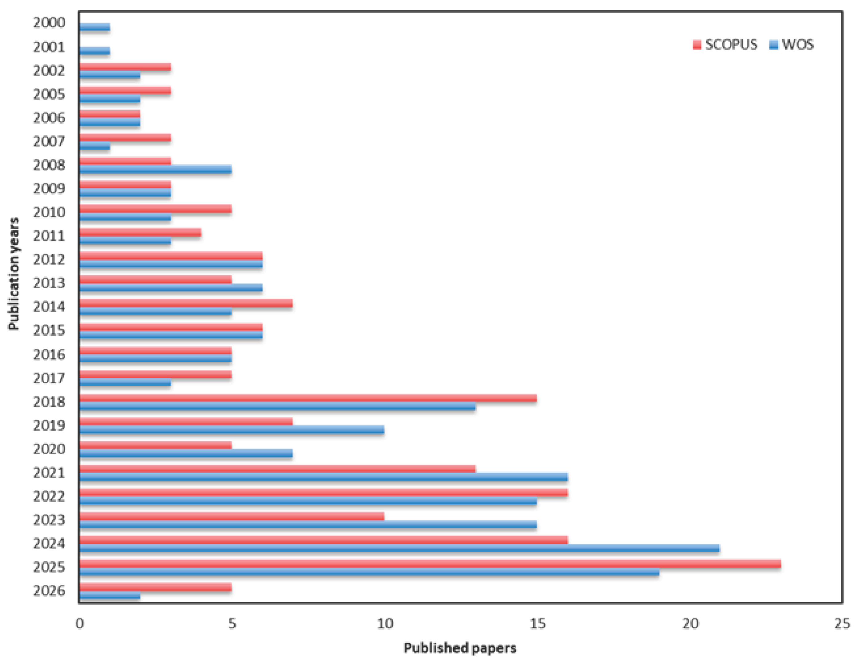
Figure 2.
Keyword co-occurrence network map (minimum keyword co-occurrence threshold of 5), generated using VOSviewer software (version 1.6.20).
Figure 2.
Keyword co-occurrence network map (minimum keyword co-occurrence threshold of 5), generated using VOSviewer software (version 1.6.20).

Figure 3.
Schematic illustration of the electroplating system used for the electrodeposition of an Ag-graphene coating on a Cu substrate. Reprinted from Sun et al. [44], Copyright: © 2024, The authors. This article is openly licensed under Creative Commons CC-BY-NC-ND-4.0.
Figure 3.
Schematic illustration of the electroplating system used for the electrodeposition of an Ag-graphene coating on a Cu substrate. Reprinted from Sun et al. [44], Copyright: © 2024, The authors. This article is openly licensed under Creative Commons CC-BY-NC-ND-4.0.
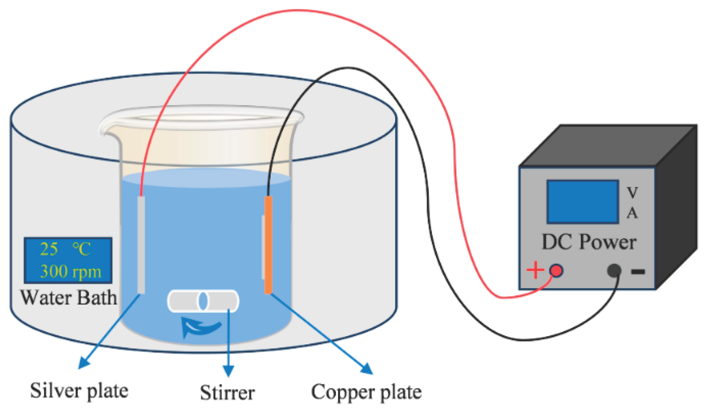
Figure 4.
Typical electrolyte components, selected examples [21,23,45,63], and their influence in the electrodeposition of Ag-based coatings.
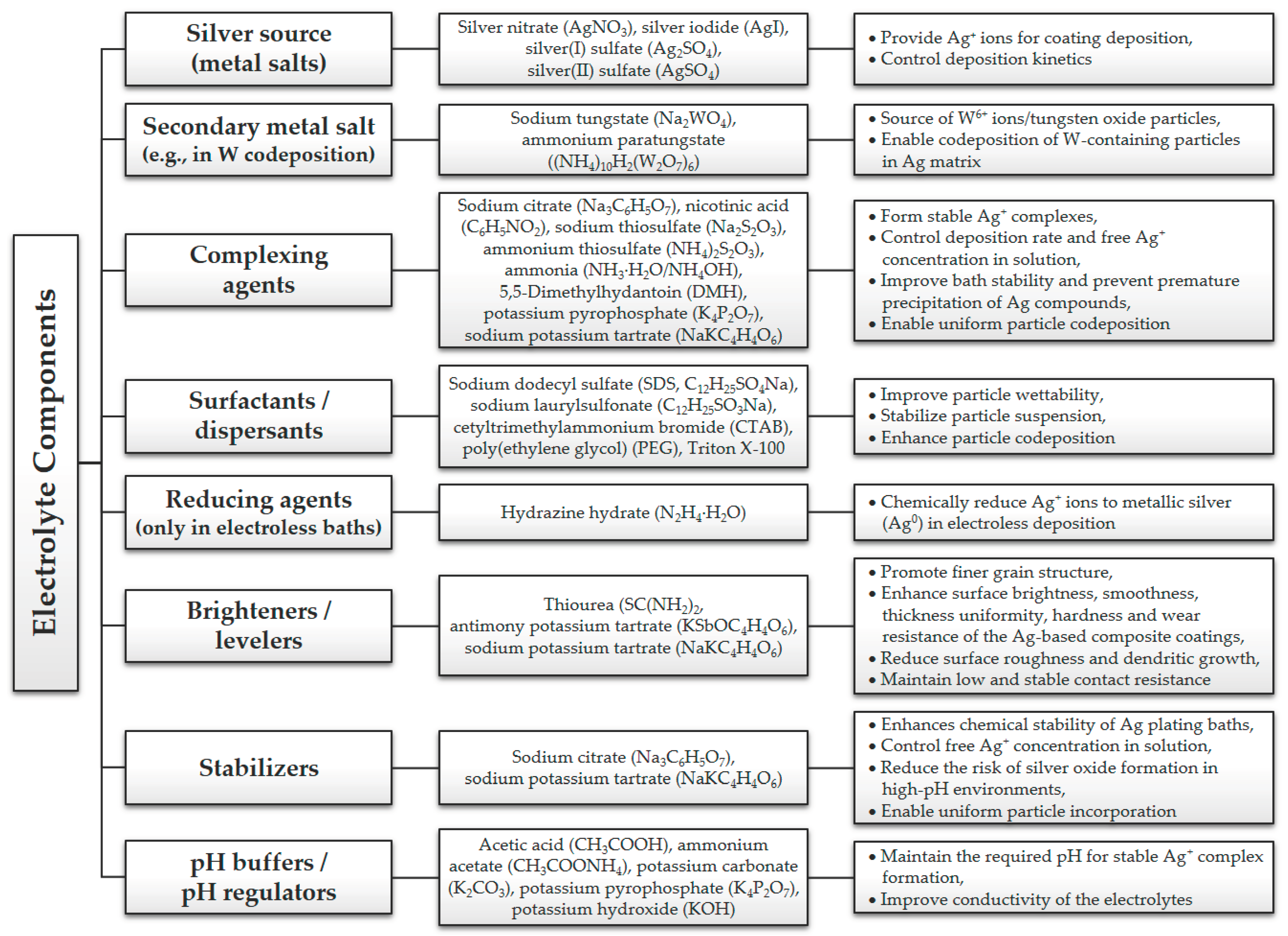
Figure 5.
Key factors affecting the properties of electrodeposited Ag-based coatings.
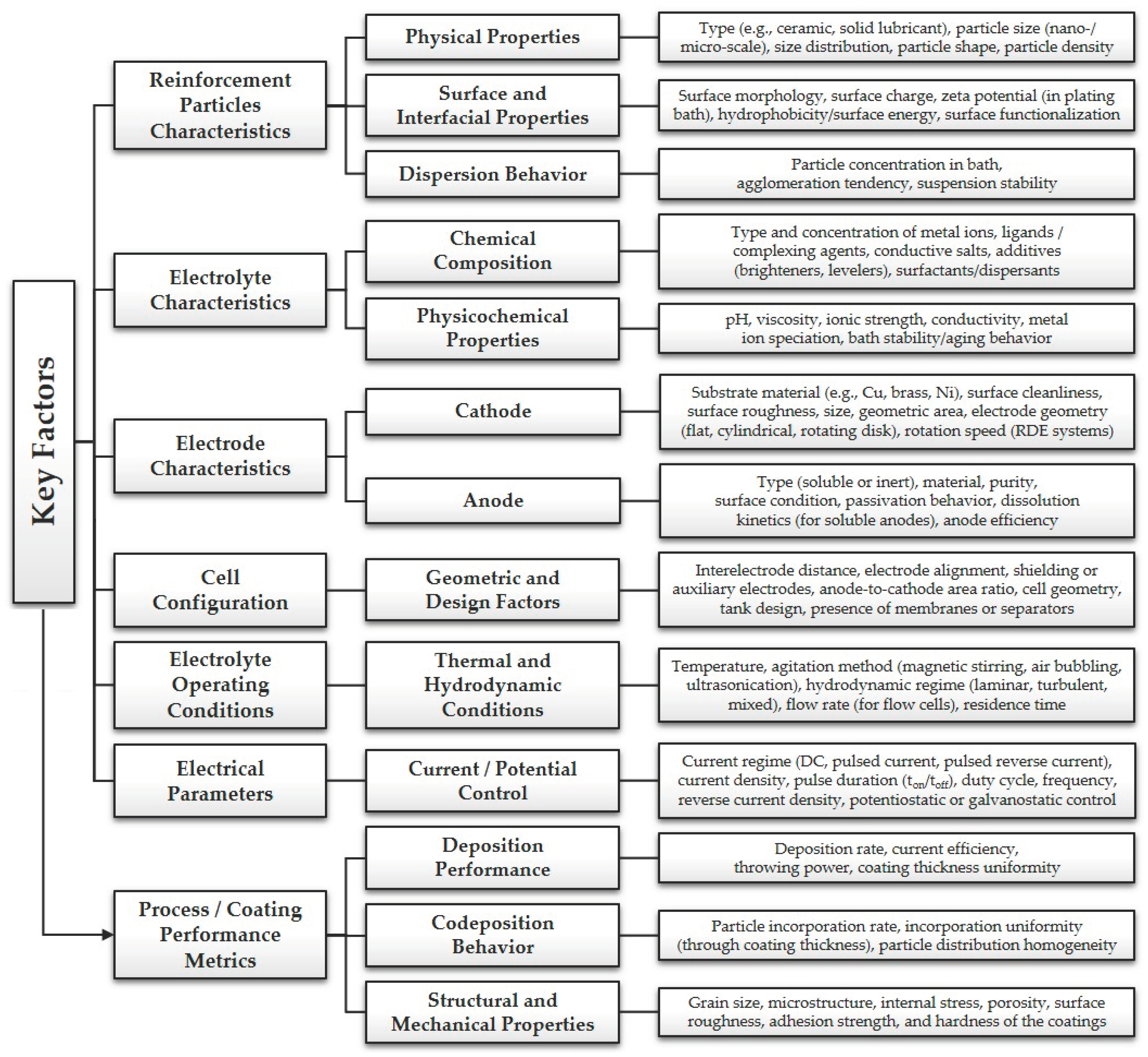
Figure 6.
Cross-sectional SEM micrograph of a 74.6 μm-thick Ag-TiB2/Cu contact electrodeposited by DC from an Ag bath containing 1 g/L TiB2 NPs. Reprinted from Cosmuş et al. [65], Copyright: © 2026, The authors. This article is openly licensed under Creative Commons CC-BY-NC-ND-4.0.
Figure 6.
Cross-sectional SEM micrograph of a 74.6 μm-thick Ag-TiB2/Cu contact electrodeposited by DC from an Ag bath containing 1 g/L TiB2 NPs. Reprinted from Cosmuş et al. [65], Copyright: © 2026, The authors. This article is openly licensed under Creative Commons CC-BY-NC-ND-4.0.
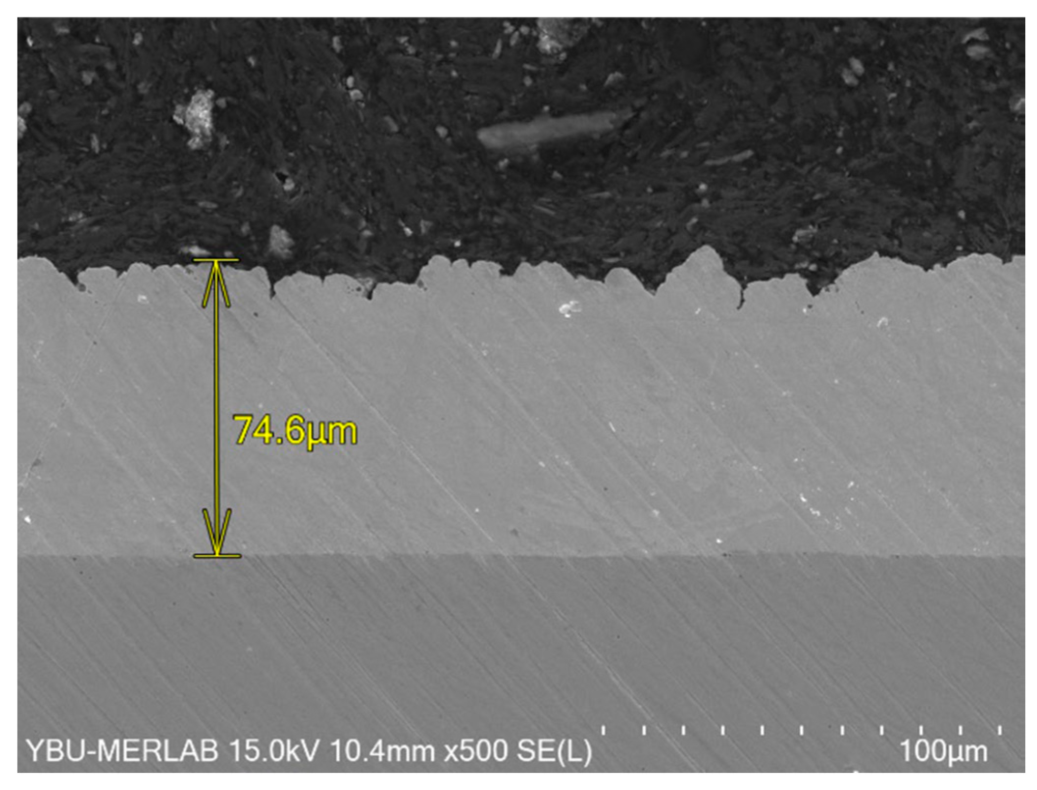
Figure 7.
Schematic illustration of the electrodeposition mechanism of an Ag-G coating on a Cu substrate using an Ag-G-nicotinic acid plating bath. Reprinted from Sun et al. [44], Copyright: © 2024, The authors. This article is openly licensed under Creative Commons CC-BY-NC-ND-4.0.
Figure 7.
Schematic illustration of the electrodeposition mechanism of an Ag-G coating on a Cu substrate using an Ag-G-nicotinic acid plating bath. Reprinted from Sun et al. [44], Copyright: © 2024, The authors. This article is openly licensed under Creative Commons CC-BY-NC-ND-4.0.
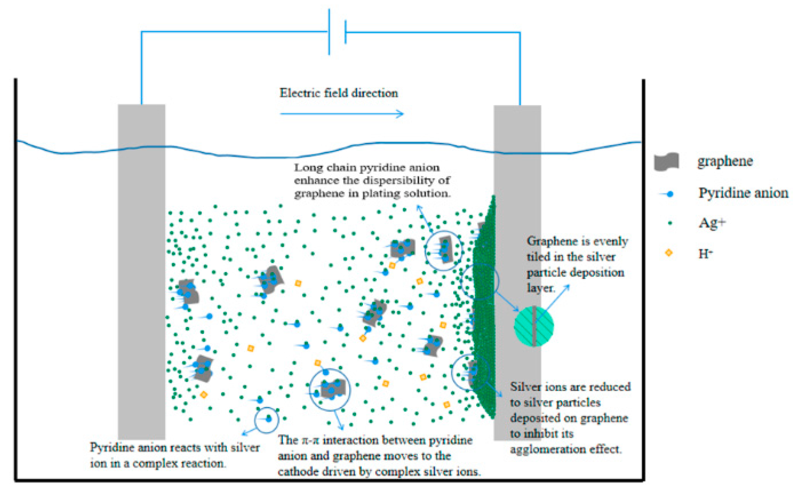
Figure 8.
Raman surface maps and morphologies of Ag-G coatings deposited on Cu substrates from (a) an Ag-G-thiosulfate plating bath and (b) an Ag-G-nicotinic acid plating bath, and schematic illustrations of the electrodeposition process under (c) graphene agglomeration and (d) uniform graphene dispersion. Reprinted from Sun et al. [44], Copyright: © 2024, The authors. This article is openly licensed under Creative Commons CC-BY-NC-ND-4.0.
Figure 8.
Raman surface maps and morphologies of Ag-G coatings deposited on Cu substrates from (a) an Ag-G-thiosulfate plating bath and (b) an Ag-G-nicotinic acid plating bath, and schematic illustrations of the electrodeposition process under (c) graphene agglomeration and (d) uniform graphene dispersion. Reprinted from Sun et al. [44], Copyright: © 2024, The authors. This article is openly licensed under Creative Commons CC-BY-NC-ND-4.0.
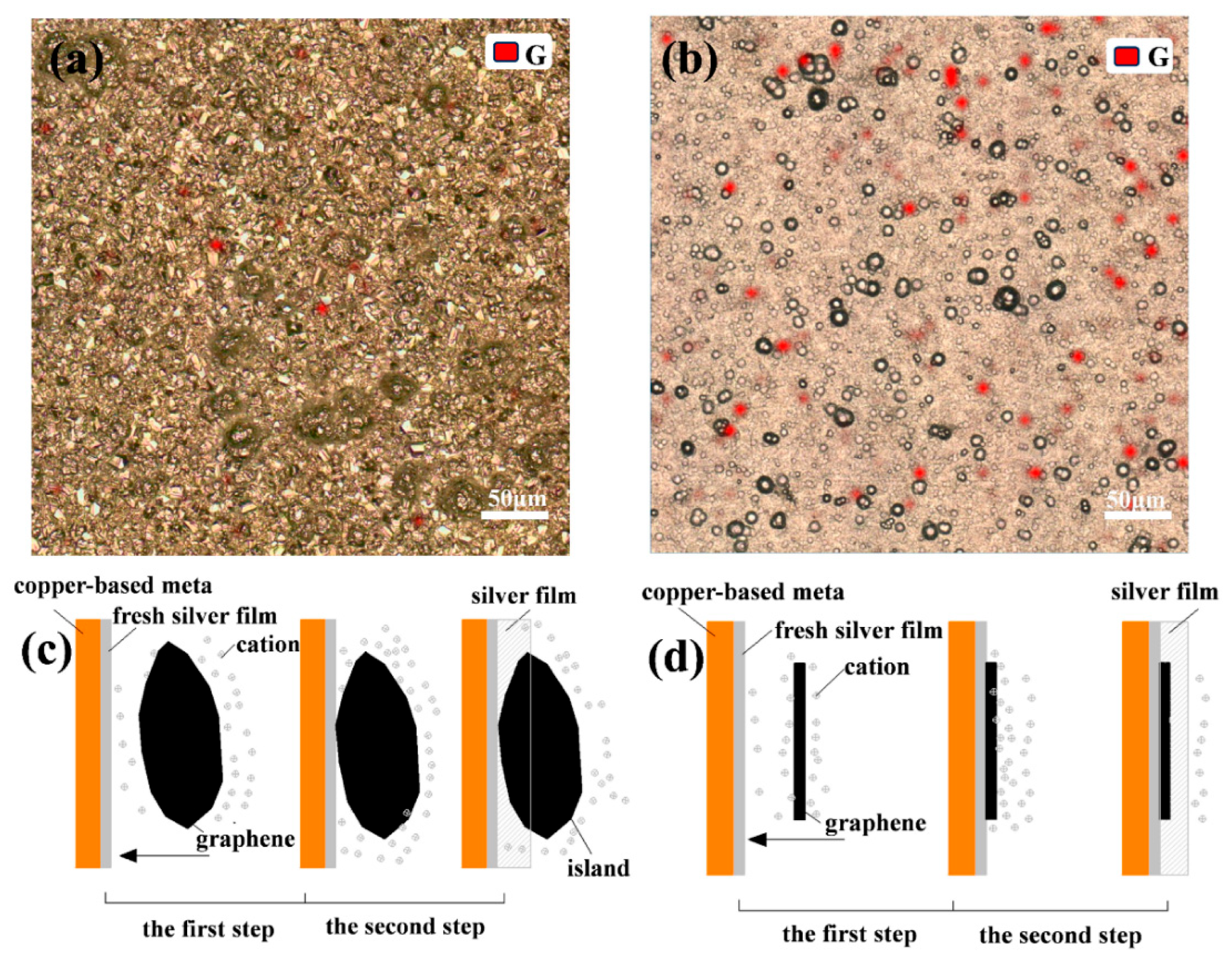
Figure 9.
Schematic illustration of the electroplating system used for the electrodeposition of an Ag-graphene coating on a Cu substrate, along with the technological flowchart for the electrodeposition and characterization of Ag-based coatings. Reprinted from Sun et al. [66], Copyright: © 2025, The authors. This article is openly licensed under Creative Commons CC-BY-NC-ND-4.0.
Figure 9.
Schematic illustration of the electroplating system used for the electrodeposition of an Ag-graphene coating on a Cu substrate, along with the technological flowchart for the electrodeposition and characterization of Ag-based coatings. Reprinted from Sun et al. [66], Copyright: © 2025, The authors. This article is openly licensed under Creative Commons CC-BY-NC-ND-4.0.
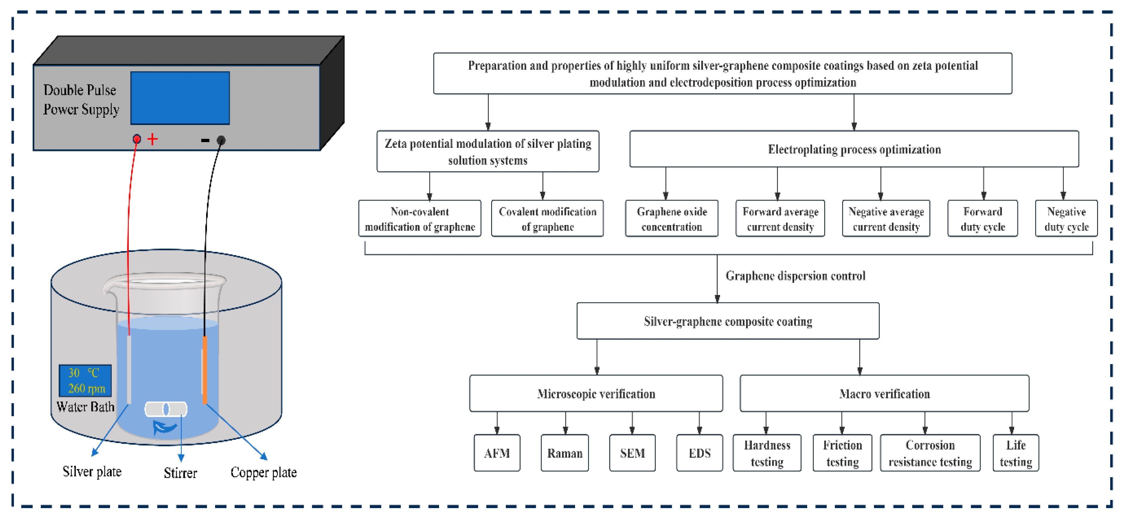
Figure 10.
Schematic illustration of the magnetron sputtering principle. Adapted from Shi et al. [67], Copyright: © 2018, The authors. Licensee IntechOpen. This article is openly licensed under Creative Commons CC-BY-3.0.
Figure 10.
Schematic illustration of the magnetron sputtering principle. Adapted from Shi et al. [67], Copyright: © 2018, The authors. Licensee IntechOpen. This article is openly licensed under Creative Commons CC-BY-3.0.
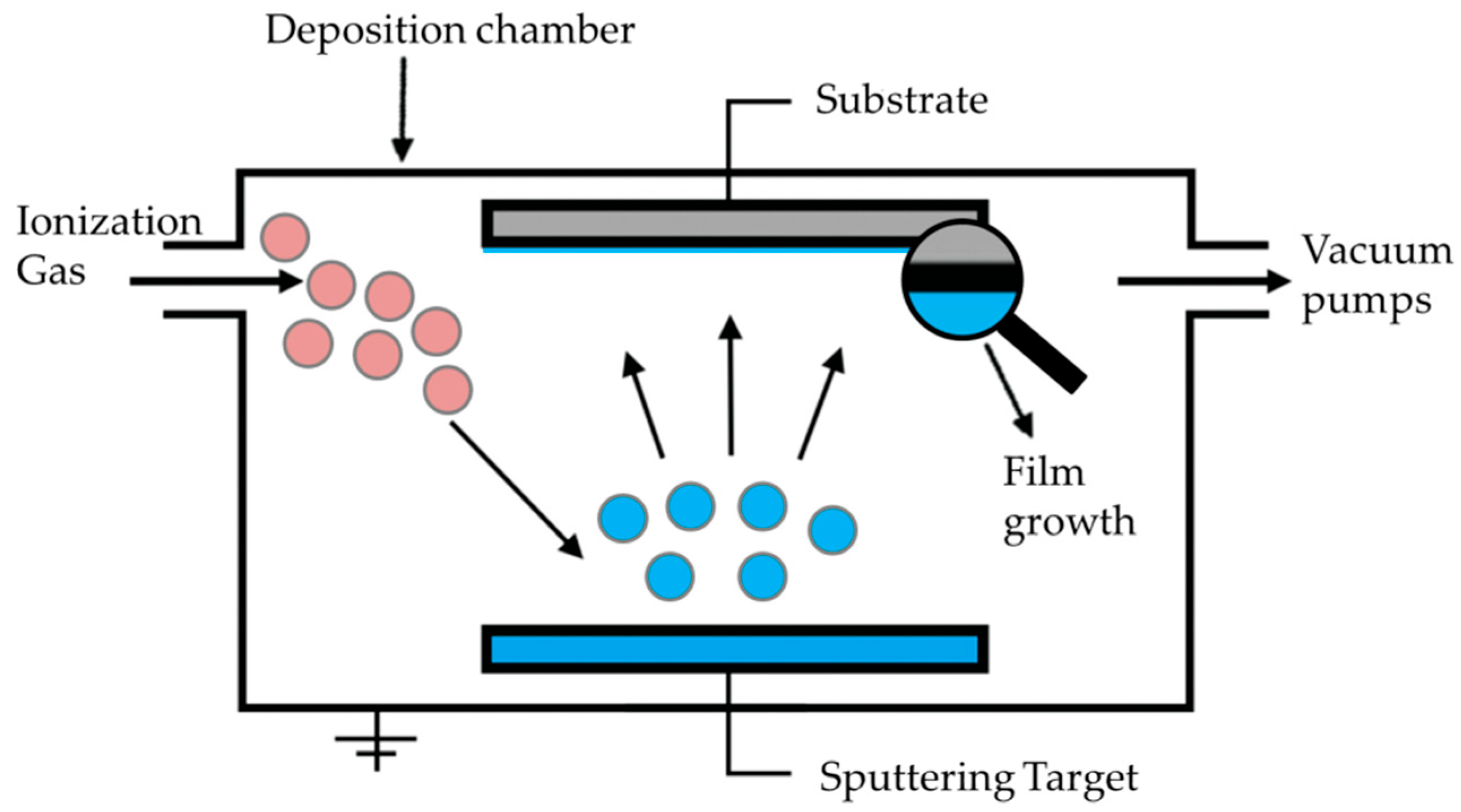
Figure 11.
Schematic illustration of the electrospark deposition principle for producing a MMC coating on a metallic substrate. Reprinted from Wang et al. [49], Copyright: © 2023, The authors. This article is openly licensed under Creative Commons CC-BY-NC-ND-4.0.
Figure 11.
Schematic illustration of the electrospark deposition principle for producing a MMC coating on a metallic substrate. Reprinted from Wang et al. [49], Copyright: © 2023, The authors. This article is openly licensed under Creative Commons CC-BY-NC-ND-4.0.
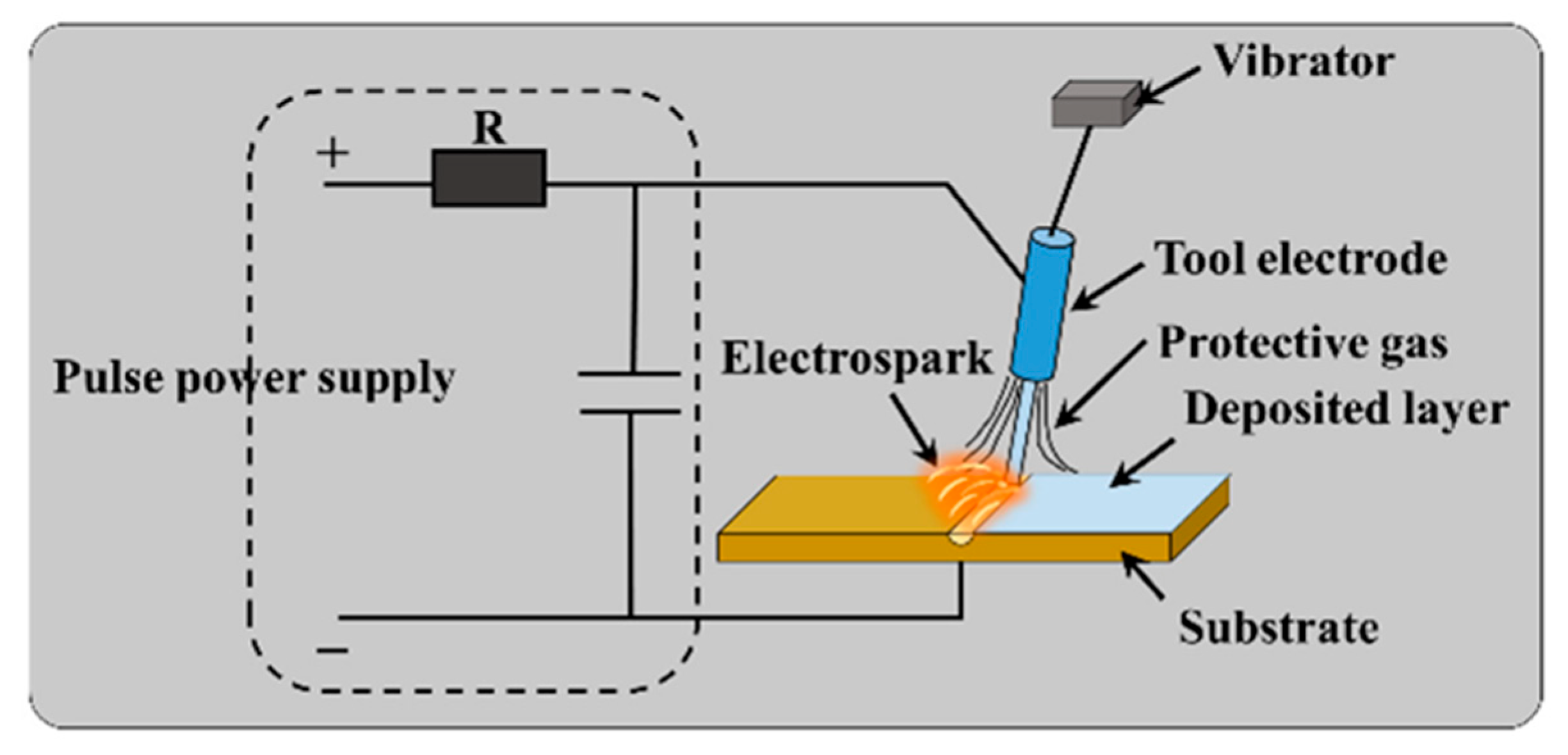
Figure 12.
Key factors affecting the properties of electrospark deposited Ag-based coatings.
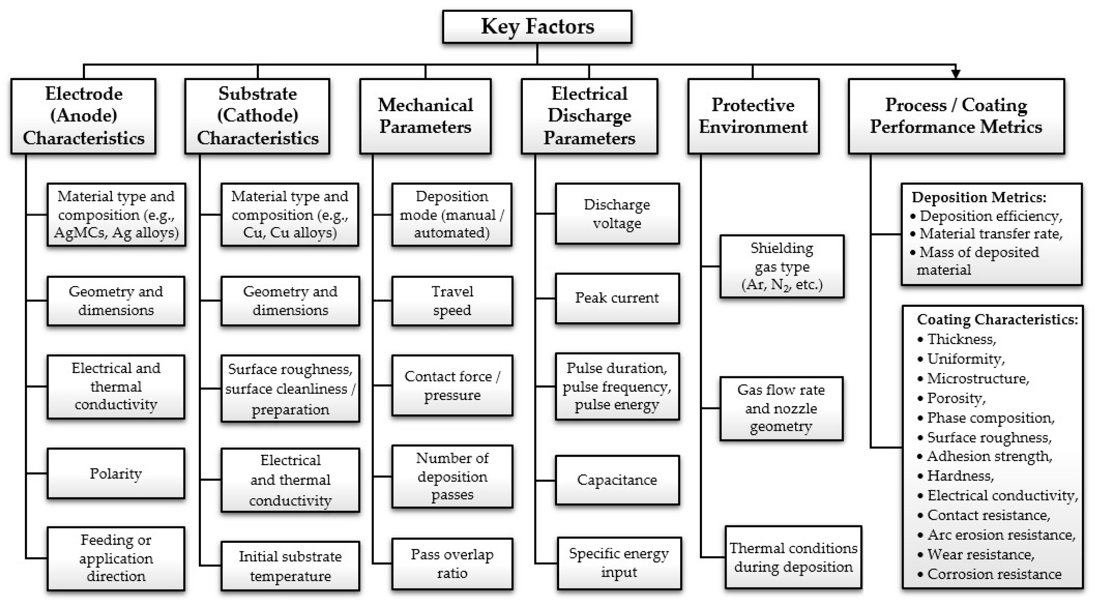
Figure 13.
Cathode mass gain as a function of time, depending on the pulsed current (Ip) passing through it: (1) Ip = 0.0 A, (2) Ip = 100 A, (3) Ip = 200 A, (4) Ip = 400 A, and (5) Ip = 600 A (equipment: EFI-10M, anode: Ag, cathode: Cu, discharge energy: 0.3 J, current pulse duration: 200 μs). Reprinted from Pereteatcu et al. [99]. Copyright: © 2013, The authors. This article is openly licensed under Creative Commons CC-BY-NC-ND-4.0.
Figure 13.
Cathode mass gain as a function of time, depending on the pulsed current (Ip) passing through it: (1) Ip = 0.0 A, (2) Ip = 100 A, (3) Ip = 200 A, (4) Ip = 400 A, and (5) Ip = 600 A (equipment: EFI-10M, anode: Ag, cathode: Cu, discharge energy: 0.3 J, current pulse duration: 200 μs). Reprinted from Pereteatcu et al. [99]. Copyright: © 2013, The authors. This article is openly licensed under Creative Commons CC-BY-NC-ND-4.0.
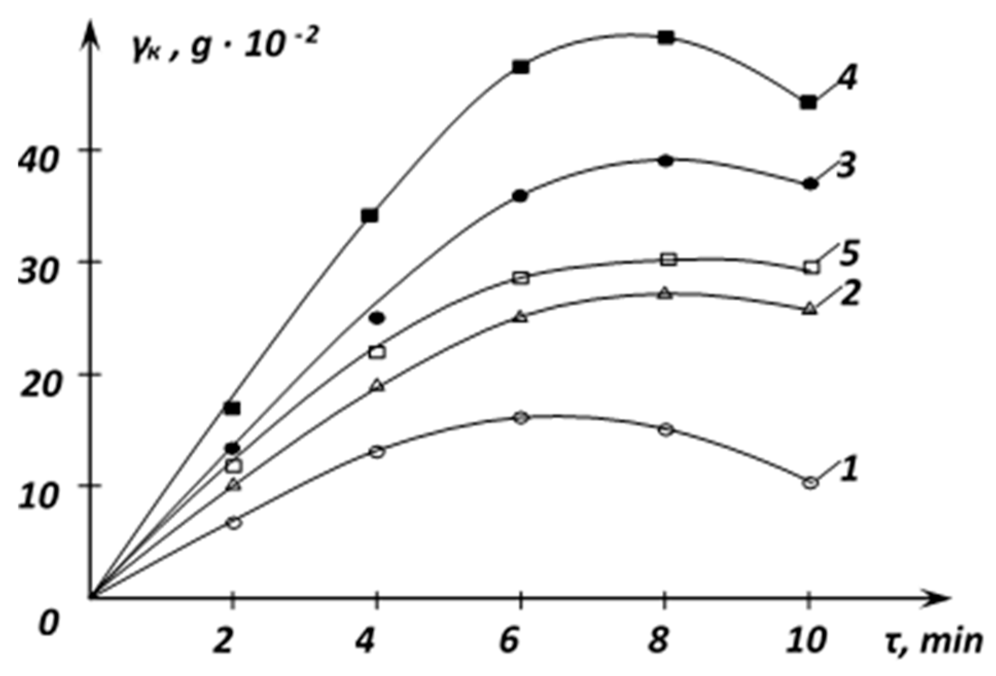
Figure 14.
Schematic illustration of (a) the thermal spraying (TS) process, (b) coating formation, (c) a commercial TS gun, (d) the TS process in operation, and the working principles of four spray methods: (e) cold spray, (f) wire arc spray, (g) plasma spray, and (h) flame spray. Reprinted from Melentiev et al. [115]. Copyright: © 2022 The Authors. Published by Elsevier Ltd. This article is openly licensed under Creative Commons CC-BY-NC-ND-4.0.
Figure 14.
Schematic illustration of (a) the thermal spraying (TS) process, (b) coating formation, (c) a commercial TS gun, (d) the TS process in operation, and the working principles of four spray methods: (e) cold spray, (f) wire arc spray, (g) plasma spray, and (h) flame spray. Reprinted from Melentiev et al. [115]. Copyright: © 2022 The Authors. Published by Elsevier Ltd. This article is openly licensed under Creative Commons CC-BY-NC-ND-4.0.
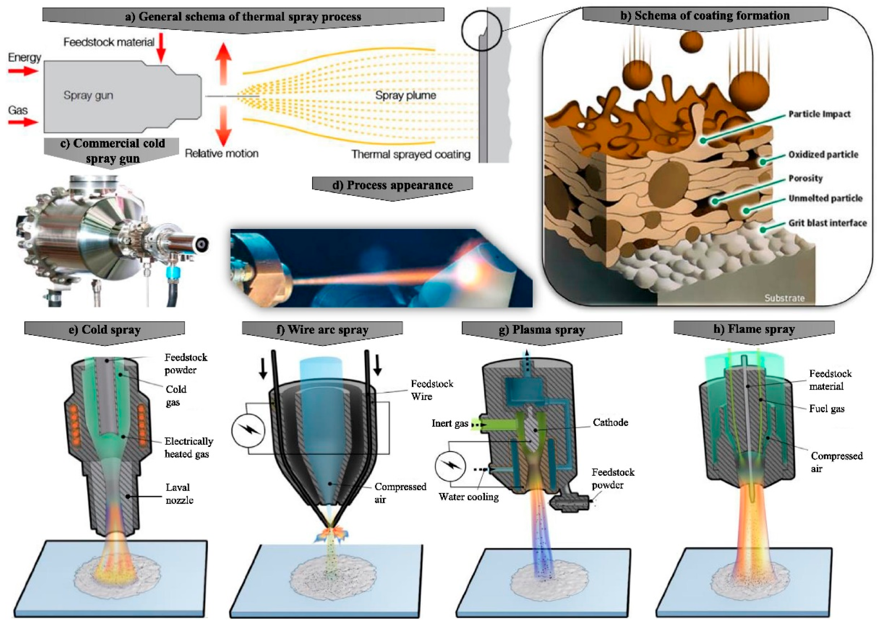
Figure 15.
Schematic mapping of thermal spray processes as a function of carrier gas temperature and particle impact velocity, with carrier gas preheated by various energy sources. Reprinted from Melentiev et al. [115]. Copyright: © 2022 The Authors. Published by Elsevier Ltd. This article is openly licensed under Creative Commons CC-BY-NC-ND-4.0.
Figure 15.
Schematic mapping of thermal spray processes as a function of carrier gas temperature and particle impact velocity, with carrier gas preheated by various energy sources. Reprinted from Melentiev et al. [115]. Copyright: © 2022 The Authors. Published by Elsevier Ltd. This article is openly licensed under Creative Commons CC-BY-NC-ND-4.0.
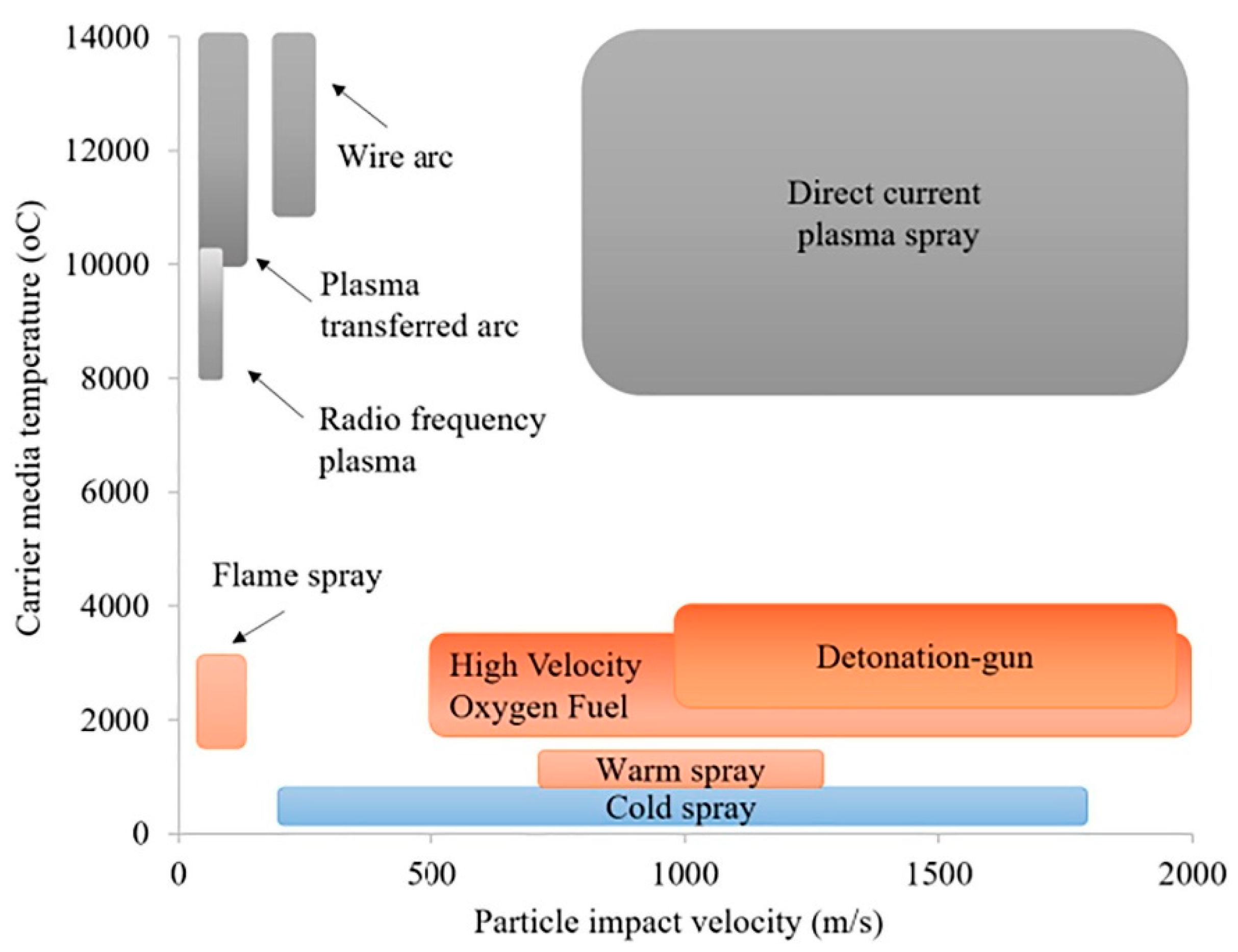
Figure 16.
Longitudinal and cross-sectional SEM micrographs of cold-sprayed 60 μm-thick Ag-C coatings deposited on Cu substrates: (a, ai) as-deposited, (b, bi) laser scanned at a scanning speed of 4000 mm/min, and (c, ci) annealed at 400 °C for 2 h. Insets display the corresponding contact angles of the Ag-C/Cu contacts under each processing condition. Reprinted from Li et al. [25]. Copyright: © 2021 The Authors. This article is openly licensed under Creative Commons CC-BY-NC-ND-4.0.
Figure 16.
Longitudinal and cross-sectional SEM micrographs of cold-sprayed 60 μm-thick Ag-C coatings deposited on Cu substrates: (a, ai) as-deposited, (b, bi) laser scanned at a scanning speed of 4000 mm/min, and (c, ci) annealed at 400 °C for 2 h. Insets display the corresponding contact angles of the Ag-C/Cu contacts under each processing condition. Reprinted from Li et al. [25]. Copyright: © 2021 The Authors. This article is openly licensed under Creative Commons CC-BY-NC-ND-4.0.
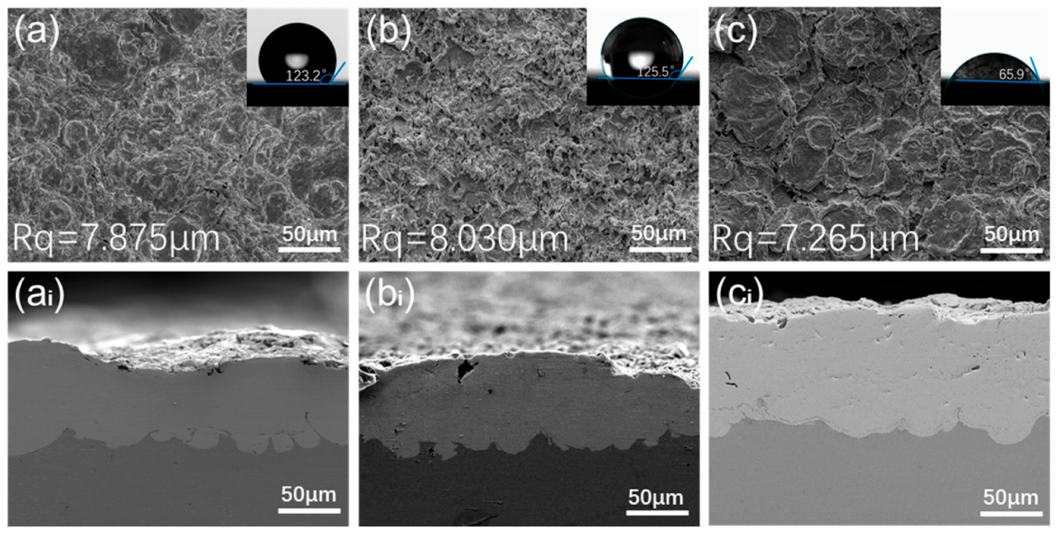
Figure 17.
Schematic illustration of an EES plasma accelerator used to produce AgMC coatings on Cu substrates: (1) inner cylindrical electrode, (2) Ag-based composite exploding conductor, (3) insulating insert, (4) discharge chamber (nozzle), (5) sample holder, (6) outer ring electrode, (7) EES-deposited sample, and (8) vacuum working chamber. Reprinted from Filyakov et al. [41], Copyright: © 2023, The authors. This article is openly licensed under Creative Commons CC-BY-NC-ND-4.0.
Figure 17.
Schematic illustration of an EES plasma accelerator used to produce AgMC coatings on Cu substrates: (1) inner cylindrical electrode, (2) Ag-based composite exploding conductor, (3) insulating insert, (4) discharge chamber (nozzle), (5) sample holder, (6) outer ring electrode, (7) EES-deposited sample, and (8) vacuum working chamber. Reprinted from Filyakov et al. [41], Copyright: © 2023, The authors. This article is openly licensed under Creative Commons CC-BY-NC-ND-4.0.
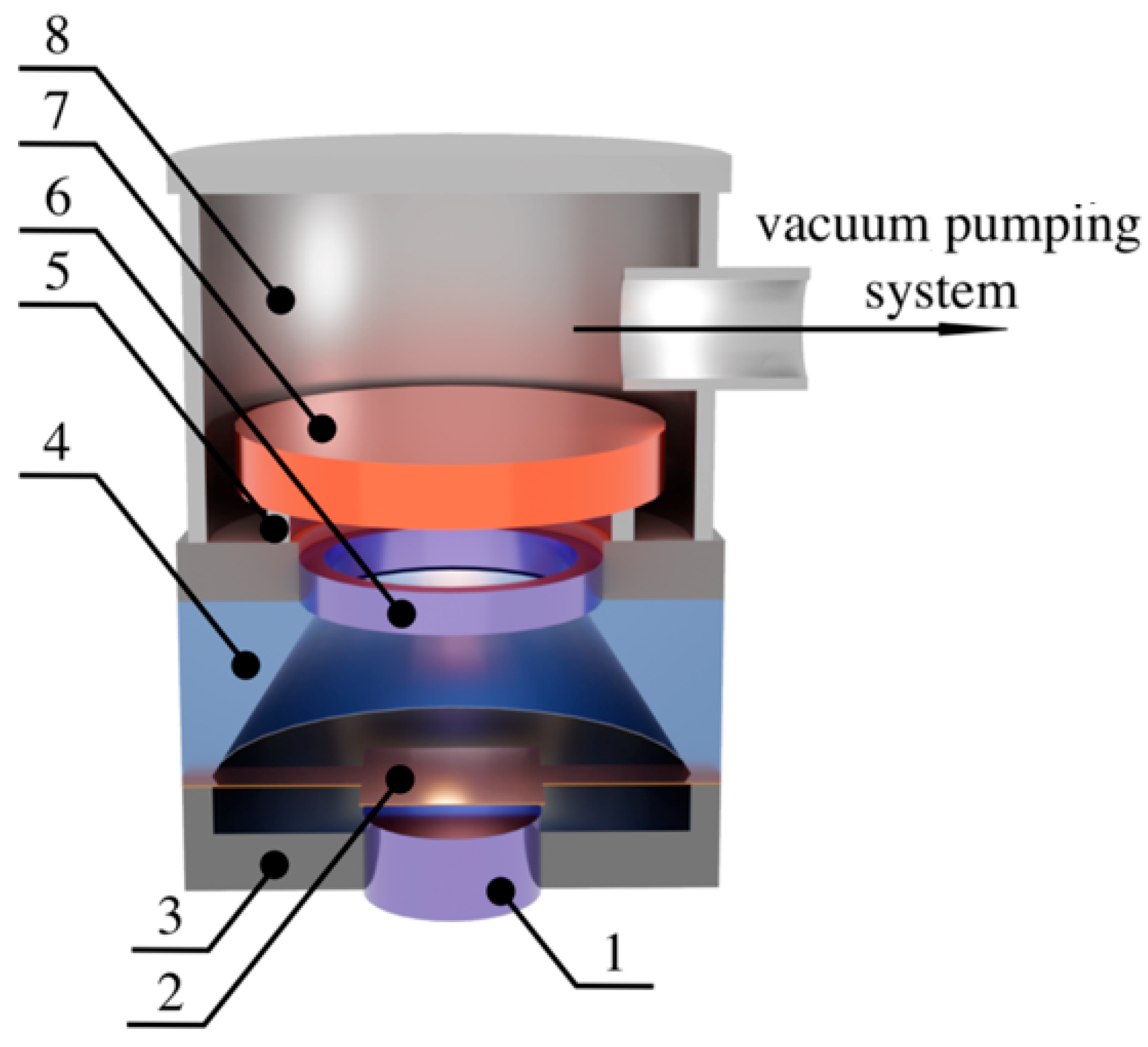
Figure 18.
Key factors affecting the properties of EES-deposited Ag-based coatings.
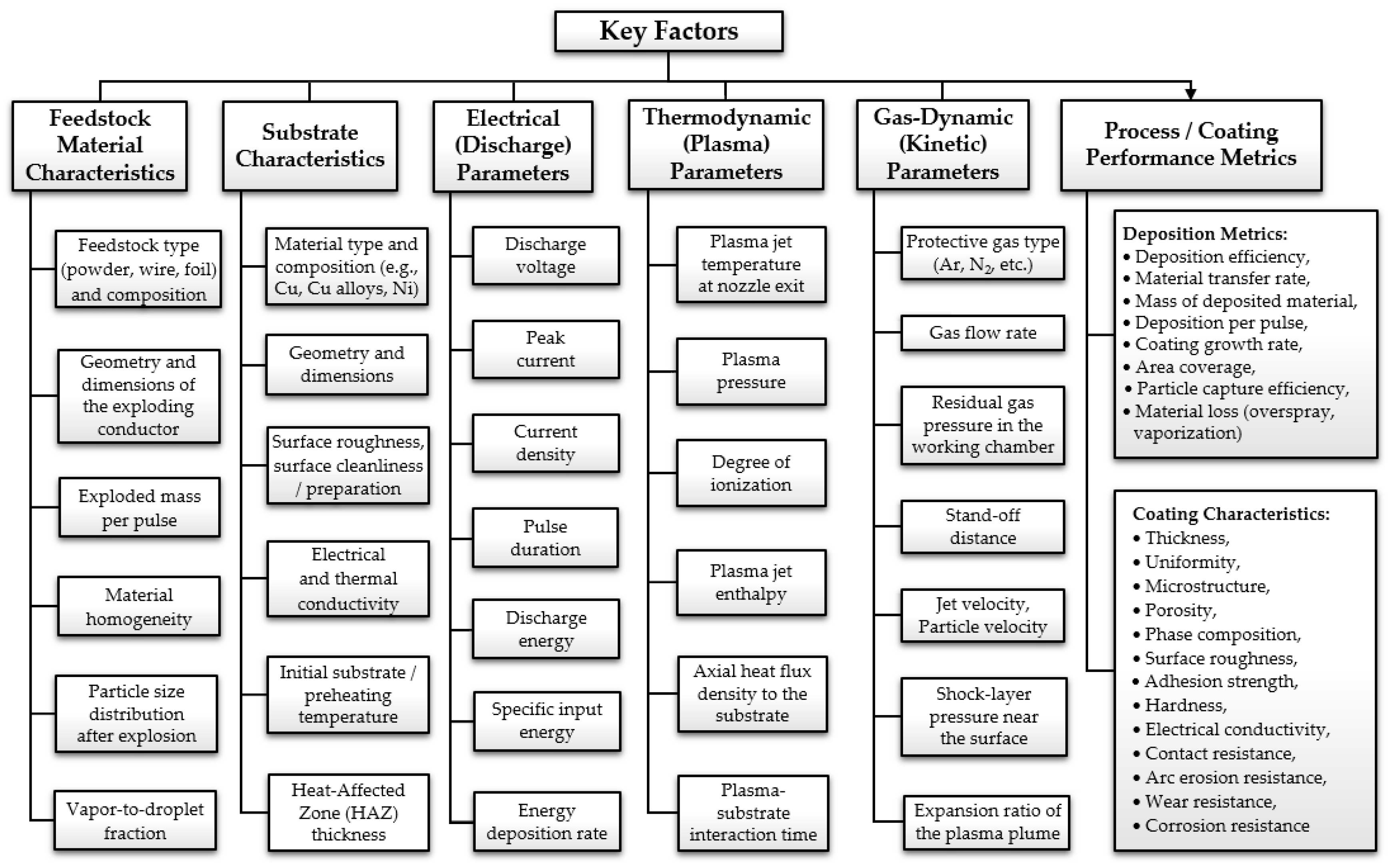
Figure 19.
Macroscopic images of an electrically exploded conductor (Ag foil with ZnO or TiB2 powders) used for producing (a) Ag-ZnO coatings and (b) Ag-TiB2 coatings on Cu substrates by EES. Reprinted from Filyakov et al. [41], Copyright: © 2023, The authors. This article is openly licensed under Creative Commons CC-BY-NC-ND-4.0.
Figure 19.
Macroscopic images of an electrically exploded conductor (Ag foil with ZnO or TiB2 powders) used for producing (a) Ag-ZnO coatings and (b) Ag-TiB2 coatings on Cu substrates by EES. Reprinted from Filyakov et al. [41], Copyright: © 2023, The authors. This article is openly licensed under Creative Commons CC-BY-NC-ND-4.0.
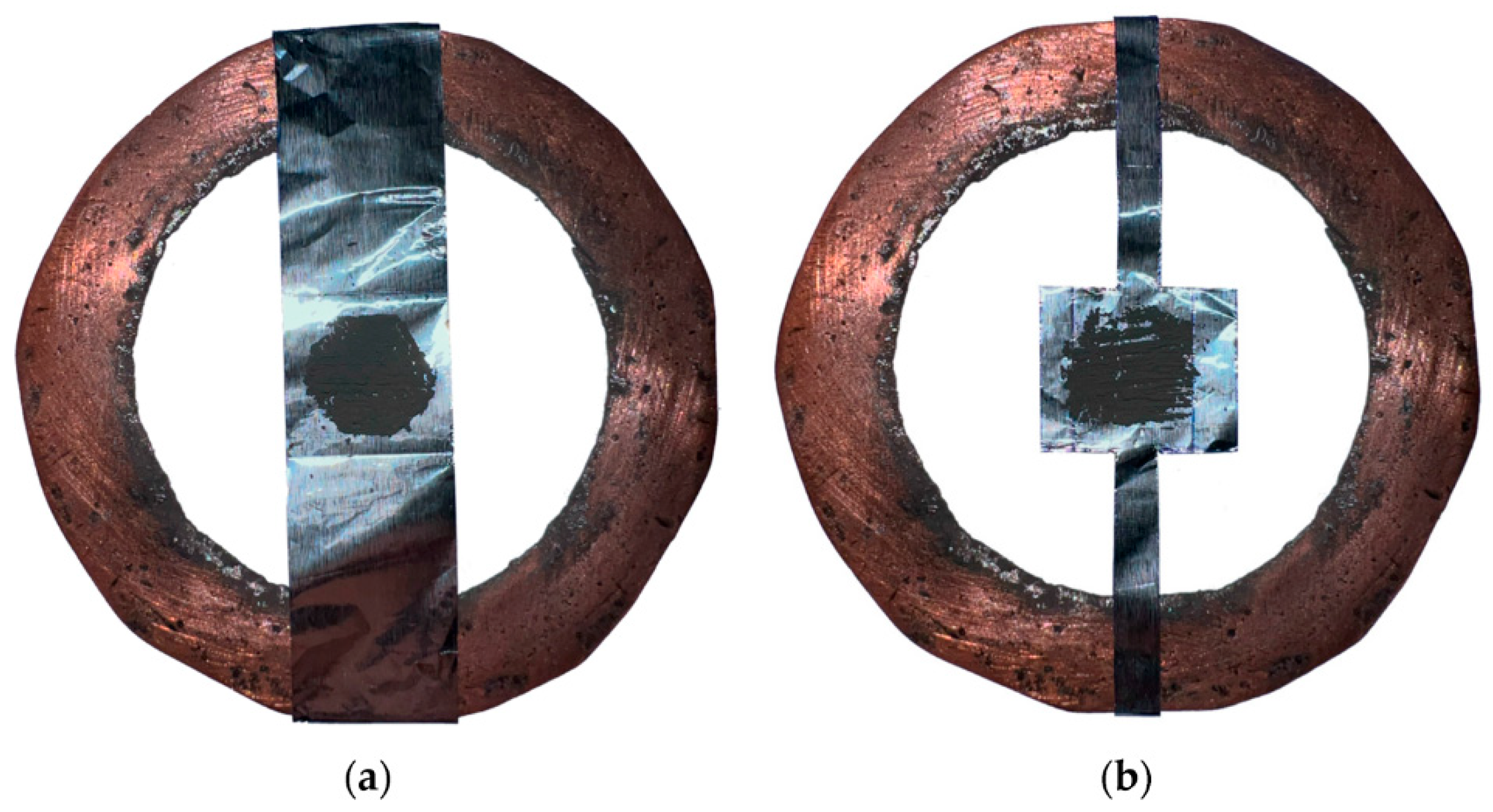
Figure 20.
Cross-sectional OM images of EES-deposited Ag-W coatings on Cu substrates at three energy modes: (a) mode 1 (U1 = 2.4 kV), (b) mode 2 (U2 = 2.5 kV), (c) mode 3 (U3 = 2.6 kV). Reprinted from Romanov et al. [34], Copyright: © 2018, The authors. This article is openly licensed under Creative Commons CC-BY-3.0.
Figure 20.
Cross-sectional OM images of EES-deposited Ag-W coatings on Cu substrates at three energy modes: (a) mode 1 (U1 = 2.4 kV), (b) mode 2 (U2 = 2.5 kV), (c) mode 3 (U3 = 2.6 kV). Reprinted from Romanov et al. [34], Copyright: © 2018, The authors. This article is openly licensed under Creative Commons CC-BY-3.0.
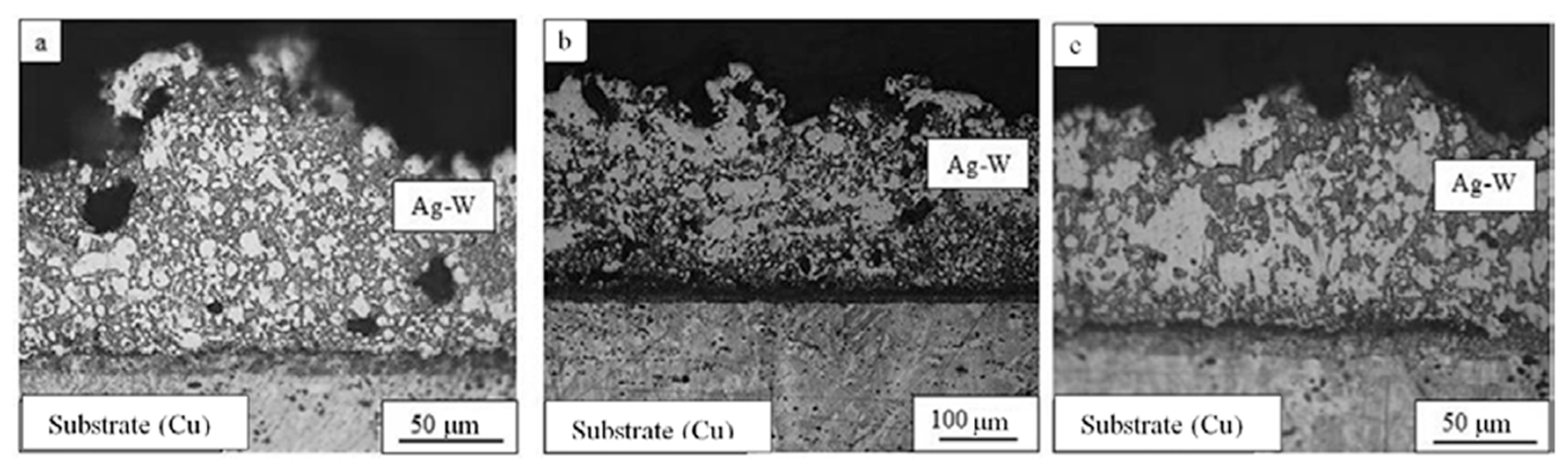
Figure 21.
Cross-sectional SEM images of EES-deposited Ag-ZnO coatings on Cu contacts showing a multilayer structure (1 - surface layer, 2 - transition layer, 3 - HAZ): (a) general view of the Ag-ZnO coating/Cu structure, (b) higher magnification image of the Ag-ZnO coating/Cu structure, and (c) image of the surface layer structure. Reprinted from Romanov et al. [40], Copyright: © 2019, The authors. This article is openly licensed under Creative Commons CC-BY-NC-ND-4.0.
Figure 21.
Cross-sectional SEM images of EES-deposited Ag-ZnO coatings on Cu contacts showing a multilayer structure (1 - surface layer, 2 - transition layer, 3 - HAZ): (a) general view of the Ag-ZnO coating/Cu structure, (b) higher magnification image of the Ag-ZnO coating/Cu structure, and (c) image of the surface layer structure. Reprinted from Romanov et al. [40], Copyright: © 2019, The authors. This article is openly licensed under Creative Commons CC-BY-NC-ND-4.0.
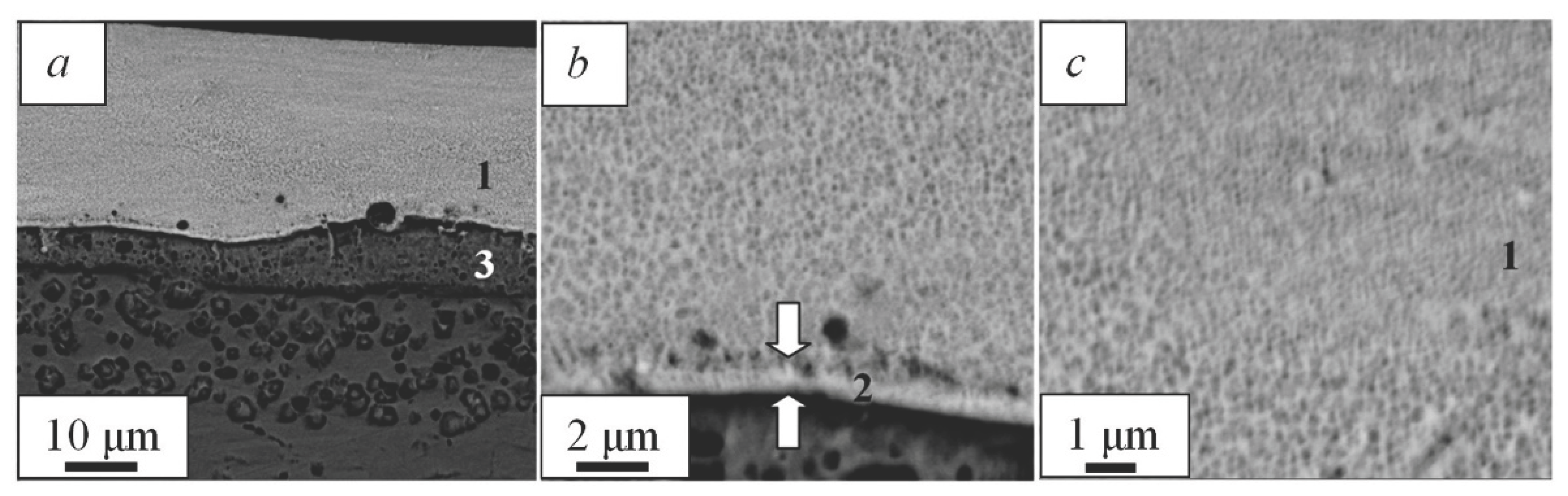
Figure 22.
Variation of the contact resistance (R) of EES-deposited Ag-ZnO coatings on Cu contacts as a function of the number of on/off cycles (N) under AC-3 conditions using a three-phase (L1, L2, L3) CJ20 electromagnetic starter. Reprinted from Romanov et al. [40], Copyright: © 2019, The authors. This article is openly licensed under Creative Commons CC-BY-NC-ND-4.0.
Figure 22.
Variation of the contact resistance (R) of EES-deposited Ag-ZnO coatings on Cu contacts as a function of the number of on/off cycles (N) under AC-3 conditions using a three-phase (L1, L2, L3) CJ20 electromagnetic starter. Reprinted from Romanov et al. [40], Copyright: © 2019, The authors. This article is openly licensed under Creative Commons CC-BY-NC-ND-4.0.
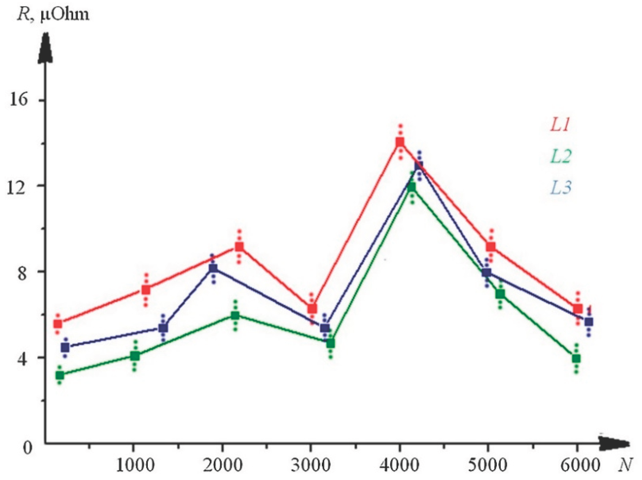

Table 1.
Selected examples of electrodeposited Ag-based coatings using Ag and other metal salts.
|
Electrolyte Composition |
Electrode Characteristics |
Synthesis Conditions |
Ag-Based Coating Characteristics |
References |
| 5 mM AgSO4, 250 mM SC(NH2)2, 285 mM Na3C6H5O7 + 30 mM, 75 mM, or 150 mM Na2WO4·2H2O |
Cathode: Cu disc (Ø6.2 mm) (rotating cylinder electrode (RCE) with 4.5 mm recess in a cylindrical Teflon holder Anode: Pt mesh |
Current density: 5–320 mA/cm2 for 10 min, under galvanostatic control, 25 °C, 10 mV/s, Electrolyte pH: 2 RCE rotation rate: 350 rpm (turbulent flow) |
Ag-W compounds with S and O with 2–18 wt.% W, Surface morphology: (i) at 5 mA/cm2: rough, plate-like for 30–75 mM Na2WO4, and smooth, nodular for 150 mM Na2WO4, (ii) at 320 mA/cm2: dendritic for 30–150 mM Na2WO4 |
[45] |
| 26 g/L AgNO3, 140 g/L DMH, 100 g/L K2CO3, 60 g/L K4P2O7, 0-4 g/L KSbOC4H4O6 (APT), 0-4 g/L NaKC4H4O6 (SPT), SPT/APT ratio of 5:1 |
Cathode: Cu sheet (10 × 20 × 5 mm3), mirror finish polished Anode: Ag sheet (20 × 35 mm2) |
Deposition time: 30 min, under galvanostatic control, RT, deposition potential: –0.8 VSCE, stirring speed: 60 rpm, Electrolyte pH: 10 |
Ag-Sb films with 0–2.72 wt.% Sb, Film thickness: 5.27–5.83 μm, Vickers hardness: 88.1–146.5 HV, COF: 0.56–0.79 (dry sliding), Wear rate: 0.84–8.64 × 10⁻⁶ mm3/N⋅m, Corrosion rate (in 3.5 wt.% NaCl solution): 1.41–38.5 × 10⁻² mm/year | [23] |
Table 2.
Selected examples of electrodeposited Ag-based composite coatings by incorporation of insoluble particles in the Ag plating baths.
Table 2.
Selected examples of electrodeposited Ag-based composite coatings by incorporation of insoluble particles in the Ag plating baths.
| Reinfor-cement Particles |
Electrolyte Composition |
Electrode Characteristics |
Synthesis Conditions |
Ag-Based Coating Characteristics |
References |
| TiB2 nano-particles (NPs) | 10 g/L AgNO3, 10 g/L KCN, 0.1 g/L sodium dodecyl sulphate (SDS), TiB2 NPs: 0.5 g/L, 1.0 g/L, 2.0 g/L, and 4.0 g/L |
Cathode: Cu contact buttons (Ø4 mm) removed from Himel HDC6-9 contactors, with surface roughness Ra: 3–5 μm Anode: high- purity Ag plate |
Bath temperature: 50 ± 1 °C, Electrolyte pH: 9–10, magnetically stirring, Process: direct current (DC) electroplating: Deposition time: 2 h, Current density: 5 A/dm2, Coating rate: 0.62 μm/min for 1.0 g/L TiB2 addition |
Pure Ag coating: Hardness: 74.1 HV, Electrical resistivity: 0.278 Ω Ag-TiB2 coating thickness: 74.6 μm (1.0 g/L TiB2), Hardness: 79.5–82.2 HV, Electrical resistivity: 0.280–0.294 Ω |
[65] |
| MWCNTs with diameter × length of 100–150 nm × 10 μm, CNT density of 2.1 g/cm3 |
0.2 M AgI, 2.5 M KI, 10 g/L CNTs |
Cathode: pure Cu plate (C1020), exposed surface area: 30 × 33.3 mm2 Anode: pure Ag plate |
(i) Current density: 30 mA/cm2, electrical charge: 9 C/cm2 (for Ag strike/Cu), (ii) Current density: 10 mA/cm2, RT, pH: 12 + aeration (for Ag/CNT film/Ag strike/Cu) |
Ag-1.2 vol.% CNT coatings, Vickers hardness: 63.2 HV, Thicknesses: NR, Electrical resistivity: 1.9 μΩ cm, COF: 0.4–0.5 (dry sliding) |
[63] |
| Graphene (G) with 1–3 layers, sheet size of 7–12 μm, and 98% carbon content |
45 g/L AgNO3, 100 g/L C6H5NO2, 77 g/L CH3COONH4, 70 g/L K2CO3, 45 g/L KOH, 32 mL/L NH3·H2O, 0.05 g/L SDS, 0.05 g/L C12H25SO3Na, 0.05 g/L PEG 400, 0.5 g/L G |
Cathode: Cu plate (50 × 50 × 0.8 mm3), exposed surface area: 30 × 10 mm2 (Ra ≤ 0.03 μm) Anode: pure Ag plate |
Current density: 0.24 A/dm2, Electrolyte stirring speed: 300 rpm, Electrolyte pH: 9.5–10, Bath temperature: 25 ± 1 °C, Bath volume: 1 L |
Ag-G coating thickness: 13–16 μm, Surface roughness Ra: 0.3 μm, Hardness: 120 HV, COF: 0.54 (dry sliding), High resistance to arc ablation |
[44] |
| Graphene (G) | (i) pre-Ag plating: 5 g/L AgNO3, 80 g/L C5H8N2O2, 30 g/L C6H5NO2, 7 g/L K2CO3, 5 g/L KOH, (ii) Ag/G plating: 45 g/L AgNO3, 100 g/L C6H5NO2, 77 g/L CH3COONH4, 30 g/L K2CO3, 45 g/L KOH, 6 mL/L NH3·H2O, 0.2 g/L SDS, 0.2 g/L C12H25SO3Na, 0.2 g/L (C6H9NO)n, 0.5–2 g/L G |
Cathode: Cu plate (50 × 50 × 5 mm3), exposed surface area: 50 × 10 mm2 Anode: Ag bar (99.99% purity) |
Current density: 0.004 A/dm2 for 120 s (pre-Ag plating), and 0.6 A/dm2 for 1.5 h (Ag/G plating), Electrolyte stirring speed: 250 rpm for 1 h, Electrolyte pH: 9.5–10, Bath temperature: 27 ± 1 °C, Double-pulse electrodeposition (DPED) |
Ag/G film thickness (DP): 40.5–41.5 μm, Hardness (DP): 125.81–161.93 HV, COF: 0.41–0.63 (dry sliding, CCF, 5 A), Surface roughness Ra: 41.3 nm and electrical contact resistance: 10 mΩ (DP-Ag/G films, 2 g/L G) |
[46] |
| Graphene (G) black powder: a few layers, sheet diameter of 7–12 μm, ≥ 98% carbon, Graphene oxide (GO): a few layers, sheet diameter of 5–10 μm, brown powder |
AgNO3: 45 g/L, C6H5NO2: 100 g/L, CH3COONH4: 76 g/L, K2CO3: 72 g/L, KOH: 45 g/L, NH3·H2O: 32 mL/L (all coatings: #1–#4) and: (i) C12H25NaO4S: 0.030 g/L, C18H29NaO3S: 0.038 g/L, (C6H9NO)n: 0.023 g/L (#1 coating), (ii) 0.75 g/L G (#2 coating), (iii) 0.75 g/L GO (#3 and #4 coatings), Deposition coating thickness: 15 ± 2 μm |
Cathode: T2 Cu violet plate (50 × 50 × 0.5 mm3), exposed surface area: 50 × 10 mm2 Anode: Ag plate (25 × 40 × 2 mm3, 99.9% purity) |
Bath temperature: 30 ± 1 °C, Electrolyte pH: 9.5–10.5, Electrolyte stirring speed: 260 rpm, Process: DC EP (#1, #2, #3), DPEP (#4), Forward current density: 0.26 A/dm2 (#1, #2, #3), and 0.45 A/dm2 (#4), Negative current density: 0.08 A/dm2 (#4), Forward duty cycle: 67.5% (#4), Negative duty cycle: 32.5% (#4) |
13.8 μm thick Ag coating (#1), 13.7–16.1 μm thick Ag-G coatings (#2–#4), Hardness (HV0.2): 92 (#1)–144.1 HV (#4), Surface roughness Ra: 25.5 nm (#4)–104.2 nm (#2), COF (dry sliding, CCF, 5 A): 0.506 (#1)–0.650 (#1), Average ECR: 30 mΩ (#4)–92 mΩ (#1) |
[66] |
Table 3.
Property comparison of Ag/G composite coatings deposited on Cu substrates by DC or DP electroplating (2 g/L graphene) and pure Ag coating [46].
Table 3.
Property comparison of Ag/G composite coatings deposited on Cu substrates by DC or DP electroplating (2 g/L graphene) and pure Ag coating [46].
| Property |
Ag/G Coating (DC, 2 g/L G) |
Ag/G Coating (DP, 2 g/L G) |
Pure Ag Coating |
Improvement in DP-deposited Ag/G Coating (2 g/L Graphene) |
| Average thickness |
46.8 μm | 41.5 μm | 40.6 μm | Comparable thicknesses, DP composite coating is 5.3 μm thinner than DC coating |
| Ag grain size | 26.037 nm | 21.560 nm | 27.065 nm | Grain refinement by synergistic DMH-NA coordination and DP deposition |
| Surface roughness (Ra) |
92.3 nm | 41.3 nm | 62.9 nm | ~34–55% reduction in Ra, yielding a smooth, dense surface |
| Average Vickers hardness |
122.04 HV | 161.93 HV | 99.20 HV | ~33–63% increase due to grain refinement and dispersion strengthening |
| Average COF (dry sliding, CCF, 5 A) |
0.63 | 0.41 | 0.72 | ~35–43% reduction in COF due to self-lubricating graphene and smoother surface |
| Average wear volume (CCF, 5 A) |
6.53 × 105 μm3 | 2.28 × 105 μm3 | 8.0 × 105 μm3 | ~65–72% reduction in wear volume due to graphene lubrication effect |
| Electrical contact life (at 5 A, 24 V) | ~0.5 × 10⁵ cycles | ~1.0 × 10⁵ cycles | ~0.23 × 10⁵ cycles | Improved electrical performance, two–fourfold increase in service life |
| Contact resistance (at 5 A, 24 V) |
6–20 mΩ |
10 mΩ | 8-60 mΩ | More stable contact resistance due to dense and smooth surface |
Table 4.
Selected examples of Ag-based coatings deposited by magnetron sputtering.
|
Sputtering Target Characteristics |
Substrate Characteristics |
Deposition Parameters |
Ag-Based Coating Characteristics |
References |
| Ag target (purity 99.999%), Grain size: 50–150 μm |
GH4169 (Inconel 718) Ni-based superalloy substrates, Dimensions: 30 × 10 × 5 mm3 |
Base pressure ≤ 1 × 10⁻³ Pa, Working gas: Ar gas, Ar flow rate: NR, Sputtering pressure: 0.5 Pa, Bias voltage: 800 V for 15 min plasma etching, 140 V during MS, Sputtering power: 150 W, Deposition time: 60 min at LT |
3.75 μm thick Ag coatings, Average hardness: ~135 HV at RT, ~84 HV at HT, Average COF: 0.56–0.8 at RT, ~0.3–0.5 at HT, Bonding force: 23 N at RT, and 16 N at HT, Wear rate: 0.31–0.44 × 10⁻⁵ mm3/N·m at RT, and 0.17–0.25 × 10⁻⁵ mm3/N·m at HT |
[17] |
| Ag-In-Cu 98-1-1 (wt.%), Ag-In-Cu 96-1-3 (wt.%), and Ag-In-Cu 94-1-5 (wt.%) disks (Ø50 mm) |
Al 6061 alloy substrates, Dimensions: 20 × 20 × 4 mm3, Surface roughness Ra: 6 nm |
Base pressure ≤ 3 × 10⁻³ Pa, Working gas: Ar gas (purity 99.99%), Ar flow rate: 15 sccm, Sputtering pressure: 0.7 Pa, Sputtering power: 20–40 W, Power density: 1.02–2.04 W/cm2, Deposition time: 1–3 min at RT |
Ag-In-Cu films, Thickness: (32.0 ± 0.6)–(103.5 ± 0.8) nm, Average surface roughness Ra: 8–12.4 nm, Surface morphology: granular texture, average grain size: 9–18 nm |
[68] |
| Ag circular target (purity 99.95%, Ø152.4 mm) Cu circular target (purity 99.99%, Ø152.4 mm) |
Ti6Al4V disk-shaped substrates, Dimensions: Ø10 mm × 1 mm |
Base pressure ≤ 5 × 10⁻⁶ Torr, Ar flow rate: 30 sccm, Sputtering pressure: 5 mTorr, Target to substrate distance: 200 mm, Substrate rotation speed: 5 rpm, HiPIMS: frequency: 250 Hz, pulse on-time: 100 μs/150 μs, peak current: 50 A/80–200 A, voltage: 989 V/593–802 V, Pmean: 1.2 kW/1.8–6 kW, Deposition rate: 0.62–0.76 nm/s for Ag target/Cu target (duty cycle: 2.5%/3.75%), Deposition time: 1 min |
Ag-Cu bimetallic coatings, Cu to Ag concentration ratio: 1.9–4.4, Crystallite sizes: 1.2–1.8 nm, Thickness: NR, Surface roughness: NR, Hardness: NR, COF: NR, Wear rate: NR |
[76] |
| Ag circular target (purity 99.9%, Ø85 mm × 5 mm) Cu circular target (purity 99.99%, Ø85 mm × 5 mm) |
Si (100) wafers, AISI 400C stainless steel substrates, Surface roughness Ra ≤ 0.02 μm |
Base pressure ≤ 3 × 10⁻³ Pa, Working pressure (Ar gas): 0.8 Pa, Bias voltage: −80 V, Duty ratio of negative bias: 75%, Sputtering current density: ~0.21 mA/mm2 and target to substrate distance: 70 mm for both Ag and Cu targets, Substrate rotation speed: 10 rpm, Deposition rate at RT: 15 nm/min for Ag, and 12 nm/min for Cu |
Total thickness of Ag/Cu multilayer films: ~2.5 μm (15 nm thick Ag layer + 4 nm, 8 nm, 12 nm, 16 nm, 20 nm thick Cu layer, denoted AC-4, AC-8, AC-12, AC-16, AC-20), Crystallite sizes: 5–9 nm, Nanoindentation hardness HIT (AC-20): 4.3 GPa, μmean (AC-20): 0.19, Wear rate (AC-20): 6.25 × 10⁻⁷ mm3/N·m |
[82] |
| CCT: Carbon target (Ø50 mm) + Ag tablet: Ø5–20 mm, Area rate of Ag/C: 0.010–0.190 |
Si (100) substrates, Dimensions: 20 × 40 × 0.5 mm3 |
Process gas: Ar gas, Ar flow rate: 4.4 sccm, Sputtering pressure: 0.11 Pa, RF power: 75 W, 125 W, and 175 W, Deposition distance: 70 mm, Deposition time: 1 h |
Ag/DLC coatings, Mean thickness: 0.1–0.9 μm, Ag content: 6–65 at.%, Structure: granular, Nanoindentation hardness (HIT): ~2.5–20 GPa, COF < 0.2 (~0.5 μm thick Ag/DLC coating with 46 at.% Ag) |
[83] |
Table 5.
Selected examples of Ag-based coatings produced by ESD/ESA on metallic substrates.
|
Electrode (Anode) Characteristics |
Substrate Characteristics |
Deposition Parameters/ Equipment Type |
Ag-Based Coating Characteristics/Remarks |
References |
| Pure Ag and Ag-3 at.% C |
Cu substrates |
Capacitance: 200 µF, Current: 1 A, Discharge: peak current Ia ≈ 220 A, peak voltage Ua ≈ 34 V, Pulse duration: ~100 µs, Pulse energy Wp ≈ 0.2 J, Mean diameter of the anode crater: 300 µm, Equipment: Elitron-22 |
Ag and Ag-C coating characteristics (thickness, phase composition, microstructure, porosity, surface roughness, adhesion strength, hardness, wear rate, conductivity, contact resistance, COF, etc.): NR | [48] |
| Pure Ag, Ni, Ag-25% Ni (SN-25), Ag-50% Ni (SN-50), and Ag-75% Ni (SN-75) |
Cu substrates |
Pulse energy: 0.04–0.155 J, Equipment: Elitron-22 |
Ag, Ni, and Ag-Ni coating thickness: 1–5 μm, Ag/Ni concentration ratio at the coating surface: 2.97 ± 0.15 (SN-25), 1.25 ± 0.10 (SN-50), 0.34 ± 0.06 (SN-75) | [95] |
| Pure Ag wire (Ø2 mm × 20–40 mm, < 30° tip) |
Cu plates (400 mm2 area, thickness: ~ 1 mm) |
Pulse energy (Wp): 0.036–0.206 J, Pulse duration (τp): 110–180 μs, Pulse current amplitude: 100–230 A, Pulse voltage amplitude: 10–34 V, Capacitance: 200–500 μF, Equipment: Elitron-22, Elitron-12 |
Ag coating characteristics: NR, Optimal Ag deposition: Wp ≈ 0.15–0.17 J, τp ≈ 135 μs, Cathode mass gain: ~23 mg/cm2, Maximum molten material transfer, with moderate vaporization losses and controlled cathode erosion. |
[100] |
| Pure Ag rod (Ø1 mm × 30–35 mm, 15° tip) |
Cu substrates |
Pulse duration: 200 µs, Pulse energy: 0.1–1 J, DC magnetic field induction: 0.01–0.1 T, DC current density: ~0.5–3 A/mm2 passing through the cathode and anode, Equipment: EFI-10M |
Ag coating characteristics: NR, Analysis of Ag quasi-regular transfer oscillations from anode to cathode and transfer mechanisms in Ag coatings on Cu substrates under ESA with a magnetic field. |
[97,98] |
| Pure Ag (99.99%) as transition coating for antifriction Babbitt B83 alloy (Ø3 mm rods) |
Tin bronze QSn10-1 substrates (25 × 29 × 4 mm3) |
Voltage: 40–60 V (Ag), 20–30 V (B83), Duty cycle: 20–30% (Ag, B83), Efficiency: 1 min/cm2 (Ag), 3 min/cm2 (B83), Travel speed: 3 mm/s, Frequency: 400 Hz, Rotation speed of the layers: 550 rpm, Ar gas (99%) flow rate: 15 L/min |
B83/Ag bilayer coatings, Total coating thickness: 30–80 µm, Surface roughness Ra: 5.97–19.43 µm, Mass transfer: 27.6–125.2 mg, Smooth, dense surface layer, compact micro-structure, and COF: ~0.177 (80 µm thick coating) |
[51] |
Table 6.
Selected examples of Ag-based coatings produced by various thermal spraying techniques on metallic substrates.
Table 6.
Selected examples of Ag-based coatings produced by various thermal spraying techniques on metallic substrates.
|
Feedstock Materials |
Substrate Characteristics |
Spraying Methodand Deposition Parameters |
Ag-Based Coating Characteristics |
References |
| Water-atomized Ag powder (spherical to irregular particles of 15–50 μm) |
Stainless steel (AISI 347) substrates |
Cold spraying (CS), Process and powder carrier gas: compressed air, Air preheat temperature: 250–450 °C, Air pressure: 1–2 MPa, Average powder particle velocity: 363–469 m/s, Stand-off distance: 15 mm |
Ag coatings, Thickness: 650 ± 25 μm, Surface roughness Ra: 6.90 ± 0.79 μm, Electrical conductivity: 35–43 MS/m Hardness (HV0.1): ~112–133 HV, Porosity: ~0.1–0.32% |
[53] |
| Gas-atomized Ag powder (spherical particles of 15–50 μm) and Ni powder (spherical to irregular particles of 10–40 μm) |
Stainless steel (AISI 316) plates, Dimensions: 25 × 25 × 3 mm3, Ø25.4 × 3 mm2, Average hardness (HV0.05): 231.3 HV |
Cold spraying (CS), Accelerating gas: N2, Gas pressure: 4 MPa, Gas temperature: 750 °C (Ni), 600 °C (Ag), Gun traverse speed: 700 mm/s (Ni), 300 mm/s (Ag), Stand-off distance: 25 mm, Multiple CS passes, Powder feed rate: 30 g/min (Ni), 50 g/min (Ag) |
Ag/Ni bilayer coatings 300 μm thick Ag top coating, Average hardness (HV0.05): 116.2 HV, 100 μm thick Ni bond layer, Average hardness (HV0.05): 172.5 HV, Porosity: < 1%, Surface roughness Ra: 4.17 ± 1.31 μm 300 μm thick Ag monolayer coating, Surface roughness Ra: 6.74 ±2.76 μm |
[101] |
| Gas-atomized Ag powder (spherical particles of 40–70 μm) |
Low carbon steel substrates, Dimensions: Ø25 × 10 mm2 |
Atmospheric plasma spraying (APS), Current: 500 A, Primary gas (Ar) flow rate: 90 scfh, No secondary gas, Carrier gas (Ar) flow rate: 7 scfh, Spraying distance: 120 mm, Gun speed: 500 mm/s |
Ag/CoNiCrAlY bilayer coatings, 200 μm thick Ag top coating, Microstructure: disk-like splat, Porosity: ~2.6%, Surface roughness: 4.59 μm, Bonding strength: 27.5 MPa, Average hardness (HV0.1): ~144 HV, 100 μm thick CoNiCrAlY bond layer | [102] |
| Ag-Ni 70-30 wt.% fine and coarse powder mixtures (initial particle size: Ag < 25 μm or 38–75 μm, Ni < 10 μm) |
Cu substrates, Dimensions: 50 × 50 × 2 mm3, Vickers hardness (HV0.5): 90 ± 2 HV |
Cold spraying (CS), Accelerating gas: N2, Inlet gas pressure: 3 MPa, Gas temperature: 400 °C, Scanning speed of the CS gun: 50 mm/s, Stand-off distance: 40 mm between the nozzle exit and the substrate, Two CS passes, Powder feed rate: ~25 g/min |
Ag-Ni coatings with fine/coarse microstructure (FM/CM) from fine/coarse Ag-Ni powder mixtures, Thickness: 2 mm, Porosity: < 1%, Ni content in the coatings: ~21 wt.% (FM), 13.8 wt.% (CM), Hardness (HV0.5): 95 HV (FM), 130 HV (CM) |
[121] |
| Ag-Ni 70-30 (irregular Ag particles of 25–38 μm, Ni particles < 5 μm), and Ag-SnO2 92-8 (spherical Ag particles < 25 μm, and SnO2 particles < 10 μm) powder mixtures |
Cu substrates, Dimensions: 50 × 50 × 2 mm3, Vickers hardness (HV0.5): 90 HV, and brass contact parts |
Cold spraying (CS), Accelerating gas: N2, Inlet gas pressure: 3 MPa, Gas temperature: 400 °C, Scanning speed of the CS gun: 50 mm/s, Stand-off distance: 40 mm between the nozzle exit and the substrate, Two CS passes, Powder feed rate: ~25 g/min |
Ag-Ni coatings, Thickness: 2 mm, Porosity: 0.64%, Ni content in the coatings: ~21 wt.%, Hardness: 95 ± 2.7 HV, Ultimate strength: 162 MPa, Young’s modulus: 98 GPa, Good erosion resistance, Ag-SnO2 coatings, Thickness: 2 mm, Porosity: 0.004%, SnO2 content in the coatings: ~2.6 wt.%, Hardness: 151 ± 1.5 HV, Ultimate strength: 202 MPa, Young’s modulus: 111.5 GPa Good erosion resistance |
[122] |
| Ag-C 97-3 wt.% powder mixture | Cu substrates, Dimensions: Ø100 mm × 5 mm |
Cold spraying (CS), Working pressure: 5 MPa, Spray distance: 30 mm, Other CS parameters: NR |
Ag-C coatings, Thickness: 60 μm, Surface roughness Rq: 7.875 μm, Electrical resistance: ~2.6 × 10⁻⁶ Ω·cm, Good arc erosion resistance under DC switching conditions (10,000 cycles, 0.8 N contact force). |
[25] |
| Water-atomized Ag-SnO2 88-12 wt.% powder, and Ag-C 95-5 wt.% powder mixture |
Cu, brass, and Al substrates, Hardness (HV0.3): 70 HV (brass), 100 HV (Cu), 130 HV(Al) |
Cold spraying (CS), Accelerating gas: N2, Inlet gas pressure: 2–3 MPa, Gas temperature: 300–600 °C, Stand-off distance: 40–60 mm between the Laval nozzle exit and the substrate, Feed rate: 25–50 g/min |
Fully densified Ag-SnO2 coatings, Thickness: 3 mm, Plate-like structure, Average hardness (HV0.3): 125 HV, Shear bonding strength: 9.5–26 MPa, Ag-C coatings tend to debond at thickness of max. 1 mm |
[123] |
| Ag-SnO2 88-12 wt.% powder (initial particle size: Ag < 70 μm, and SnO2: 30–50 nm) |
Cu substrates, Dimensions: NR | Atmospheric plasma spraying (APS), Current: 330 A, Voltage: 95 V, Primary gas (Ar) flow rate: 95 L/min, Secondary gas (H2) flow rate: 10 L/min, Carrier gas (Ar) flow rate: 4 L/min, Powder feed rate: 25 g/min, Spraying distance: 100 mm |
Fully densified Ag-SnO2 coatings, Thickness: 600 μm, Splat-like morphology, lamellar structure, Average hardness (HV0.2): 109 HV, Average bonding strength: 17.9 MPa, Low arc erosion rate: 39.9 μg/C (under 500 discharge cycles). |
[124] |
Table 7.
Selected examples of EES-deposited Ag-based composite coatings.
|
Feedstock Materials |
Substrate Characteristics |
Deposition Parameters |
Ag-Based Composite Coating Characteristics |
References |
| Ag foil (0.2463 g) filled with a W powder (0.434 g) |
Electrolytic Cu (KPV-604 contacts), Mean roughness Ra: 25.397 nm, Mean hardness: 119.4–122 HV |
Plasma action time: ~100 μs, Absorbed power density on the jet axis: ~8.2 GW/m2, Shock-layer pressure (near surface): ~18.8 MPa, Energy modes (coaxial electrode voltage): U1 = 2.4 kV, U2 = 2.5 kV, U3 = 2.6 kV |
Ag-W coatings, Thickness: (49.04 ± 0.7)–(68.5 ± 0.9) μm, Average surface roughness Ra: 75.412 nm (mode 2/U2), Average hardness: ~382 HV (mode 1/U1)–457.5 HV (mode 2/U2) |
[34] |
| Ag foil (0.25 g) filled with a CuO powder (0.12 g) |
Electrolytic Cu (KPV-604 contacts) |
Plasma action time: ~100 μs, Absorbed power density on the jet axis: ~5.5 GW/m2, Shock-layer pressure (near surface): ~12.5 MPa, Residual gas pressure in the working chamber: ~100 Pa, Plasma temperature at the nozzle exit: ~104 K, Heat affected zone thickness: ~50 μm |
Ag-CuO coatings, Thickness: 75–95 μm, Microstructure: Ag matrix with CuO inclusions (2–500 nm), Roughness Ra: 73 nm, Twofold increase in service life, contact resistance: 4–15.7 μΩ (at 400/230 V, 320 A, 50 Hz, cosϕ = 0.35, N = 6000 commutation cycles) |
[35] |
| Ag foil (0.25 g) filled with a CdO powder (0.05 g) |
Electrolytic Cu (KPV-604 contacts) |
Plasma action time: ~100 μs, Absorbed power density on the jet axis: ~5.5 GW/m2, Shock-layer pressure (near surface): ~12.5 MPa, Residual gas pressure in the working chamber: ~100 Pa, Plasma temperature at the nozzle exit: ~104 K |
Ag-CdO coatings, Thickness: ~60 μm, Microstructure: Ag matrix with inclusions of Cu (20–50 nm), Cd3Cu4 (30–40 nm), CdO2 (15–50 nm), and Ag2O3 (5–10 nm) |
[38] |
| Ag foil (0.25 g, 20 μm thick) filled with a ZnO powder (0.08 g) |
Electrolytic Cu (CJ20 contacts) |
Plasma action time: ~100 μs, Absorbed power density on the jet axis: ~5.5 GW/m2, Shock-layer pressure (near surface): ~12.5 MPa, Residual gas pressure in the working chamber: ~100 Pa, Plasma temperature at the nozzle exit: ~104 K |
Ag-ZnO coatings, Thickness: 30–60 μm, Microstructure: Ag matrix with ZnO inclusions (2–15 nm), Twofold increase in service life, ECR: 3.2–14.1 μΩ (at 400/230 V, 320 A, 50 Hz, cosϕ = 0.35, N = 6000 commutation cycles) |
[40] |
| Ag foil (0.25 g) filled with a SnO2 powder (0.05 g) |
Electrolytic Cu (KPV-604 contacts) |
Plasma action time: ~100 μs, Absorbed power density on the jet axis: ~5.5 GW/m2, Shock-layer pressure (near surface): ~12.5 MPa, Residual gas pressure in the working chamber: ~100 Pa, Plasma temperature at the nozzle exit: ~104 K |
Ag-SnO2 coatings, Thickness: NR, Crystallite size: 20–40 nm, Microstructure: Ag matrix with inclusions of SnO2, Ag3Sn, Ag4Sn, Cu6Sn5, Cu10Sn3, Cu3Sn, and CuO (20–50 nm) |
[39] |
| Ag foil (99.9%) filled with a TiB2 powder (0.2 g) |
Cu substrates (grade M00) |
Plasma action time: ~100 μs, Absorbed power density on the jet axis: ~5.5 GW/m2, Shock-layer pressure (near surface): ~12.5 MPa, Residual gas pressure in the working chamber: ~100 Pa, Plasma temperature at the nozzle exit: ~104 K |
Ag-TiB2 coatings, Thickness: 100 μm, Morphology: coarse (3–50 µm) and fine droplets (< 1 µm), Microstructure: Ag matrix with different phase composition (TiB, Cu2O, Cu, Cu4Ti3, AgTi, B2O3, B2O) and pore sizes: ~0.36–2 µm |
[41] |
| Ag-4 wt.% graphite (C) powder mixture (particle size: ≤ 32 μm) |
Cu plates (20 × 20 × 3 mm3) |
Base pressure: 10 Pa, Process gas: Ar gas, Spraying pressure: 1.5 × 10⁵ Pa, Initial charging voltage U0: 11–14 kV, Ag-C powder amount/ single spraying: 50 mg, Stand-off distance: 18 mm |
Ag/C coatings, Thickness: 20–50 μm, Coating area/single spraying: 39.25 mm2 at 13 kV, 102 mm2 at 11 kV, Deposition efficiency: 23–35%, Adhesion: good (metallurgical bonding) |
[26] |
Table 8.
Properties of Ag-based coatings produced by different deposition technologies.
|
Coating/ Substrate Type (Deposition Technique) |
Thick- ness (μm) |
Surface Rough- ness Ra (nm) |
Vickers Hard- ness HV |
Bonding Force (N)/ Strength (MPa) |
Electrical Conduc-tivity (MS/m) |
Coefficient of Friction (Dry Sliding) |
Wear Rate (mm3/N⋅m) |
Electrical Contact Resistance (mΩ) |
References |
| Ag/Cu (EP) | 5.27 | – | 88.1 | – | ~32.2 | 0.79 | 8.64 × 10⁻⁶ | – | [23] |
| Ag-2 wt.% Sb/Cu (EP) |
5.66 | – | 146.5 | – | ~6.0 | 0.56 | 0.84 × 10⁻⁶ | – | [23] |
| Ag-2.72 wt.% Sb/Cu (EP) |
5.54 | – | 140.0 | – | ~4.1 | 0.69 | 4.51 × 10⁻⁶ | – | [23] |
| Ag/Cu (EP) | – | – | 60.4 | – | ~55.6 | 0.60 | – | – | [63] |
| Ag-1.2 vol.% CNT/Ag/Cu (EP) | – | – | 63.2 | – | ~52.6 | 0.40–0.50 | – | – | [63] |
| Ag-G/Cu (EP, 0.5 g/L G) |
13–16 | 300 | 120 | – | – | 0.54 | – | [44] | |
| Ag/Cu (EP) |
40.6 | 62.9 | 99.2 | – | – | 0.72 (CCF, 5 A) |
– | 8–60 (CCF, 5 A) |
[46] |
| Ag-G/Cu (DPEP, 2 g/L G) |
41.5 | 41.3 | 161.93 | – | – | 0.41 (CCF, 5 A) |
– | 10 (CCF, 5 A) |
[46] |
| Ag-G/Cu (DCEP, 2 g/L G) |
46.8 | 92.3 | 122.04 | – | – | 0.63 (CCF, 5 A) |
– | 6–20 (CCF, 5A) |
[46] |
| Ag/Cu (EP) |
13.8 | 26.1 | 92 | – | – | 0.650 | – | 92 (CCF, 5 A) |
[66] |
| Ag-G/Cu (DPEP, 0.75 g/L G) | 13.7– 16.1 |
25.5 | 144.1 | – | – | 0.506 (CCF, 5 A) |
– | 30 (CCF, 5 A) |
[66] |
| Ag/Inconel 718 (MS) |
3.75 | – | 135 | 23 N | – | 0.56–0.80 | 3.1– 4.4 × 10⁻⁶ |
– | [17] |
| Ag/steel (CS) |
650 ± 25 | 6900 ± 790 |
112– 133 |
– | 35–43 | – | – | – | [53] |
| Ag/Ni/steel (CS) |
300/ 100 |
4170 ± 1310 |
116.2/ 172.5 |
– | – | – | – | – | [101] |
| Ag/CoNiCrAlY/ steel (CS) |
200/ 100 |
4590 | ~144 | 27.5 MPa | – | – | – | – | [102] |
| Ag-13.8 wt.% Ni/Cu (CS) |
2000 | – | 95 (CM) |
– | – | – | – | – | [121] |
| Ag-21 wt.% Ni/Cu (CS) |
2000 | – | 130 (FM) |
– | – | – | – | – | [121] |
| Ag-21 wt.% Ni/Cu (CS) |
2000 | – | 95 ± 2.7 (CM) |
– | – | – | – | – | [122] |
| Ag-2.6 wt.% SnO2/Cu (CS) |
2000 | – | 151 ± 1.5 |
– | – | – | – | – | [122] |
| Ag-5% C/Cu (CS) | 60 | – | – | ~38.5 | – | – | – | [25] | |
| Ag-SnO2/Cu (CS) |
3000 | – | 125 | 9.5– 26 MPa |
– | – | – | – | [123] |
| Ag-SnO2/Cu (APS) | 600 | – | 109 | 17.9 MPa | – | – | – | [124] | |
| Ag-W/Cu (EES) |
~49–69 | 75.412 | 382– 457.5 |
– | – | – | – | – | [34] |
| Ag-CuO/Cu (EES) |
75–95 | 73 | – | – | – | – | – | 0.004– 0.016 |
[35] |
| Ag-ZnO/Cu (EES) |
30–60 | – | – | – | – | – | – | 0.003– 0.014 |
[40] |
Table 9.
Key performance findings and dominant mechanisms of Ag-based coatings produced by different deposition technologies.
Table 9.
Key performance findings and dominant mechanisms of Ag-based coatings produced by different deposition technologies.
| Coating/Substrate Type (DepositionTechnique) |
Key Performance Findings |
Dominant Mechanisms |
References |
| 5.27–40.6 μm thick Ag/Cu (Electroplating) |
High conductivity (~32.2–55.6 MS/m), low hardness (~60–99 HV), high friction (COF: ~0.6–0.8), and lower wear resistance than Ag-based composite coatings |
Soft FCC Ag metal, adhesive wear, plastic deformation |
[23,46, 63,66] |
| 5.5–5.7 μm thick Ag-2–2.72 wt.% Sb/Cu (Electroplating) |
Lower electrical conductivity (~4.1–6 MS/m), higher hardness (~140–146.5 HV), and improved tribological behavior (COF = 0.56–0.69) compared with 5.27 μm thick Ag coatings (~32.2 MS/m, 88.1 HV, COF = 0.79) |
Solid-solution strengthening, electron scattering, abrasive and adhesive wear, plastic deformation | [23] |
| Ag-1.2 vol.% CNT/Ag/Cu (Electroplating) |
Slightly lower conductivity (~52.6 MS/m), higher hardness (~63.2 HV), lower friction (COF: ~0.4–0.5), and improved wear resistance compared with pure Ag coatings (~55.6 MS/m, 60.4 HV, COF: ~0.6) | Load transfer strengthening, CNT-based solid lubrication, lubricious tribofilm formation |
[63] |
| Ag-G/Cu (EP, 0.5–2 g/L G) |
Higher hardness (~120–122 HV), lower (COF: 0.54–0.63), and lower ECR (6–30 mΩ) under dry sliding and current-carrying friction (CCF, 5 A) than pure Ag coatings (92–99 HV, COF: ~0.65–0.72, ECR: 8–92 mΩ) | Load transfer strengthening, graphene-based solid lubrication, lubricious tribofilm formation | [44,46, 66] |
| Ag-G/Cu (DPEP, 0.75–2 g/L G) |
Finer grains, higher hardness (~144–162 HV), lower friction (COF: ~0.41–0.51), and lower ECR (10–30 mΩ) under dry sliding and CCF (5 A) than pure Ag coatings | Pulsed nucleation, graphene-based solid lubrication |
[46,66] |
| (3.75 μm thick Ag/Inconel 718 (Magnetron sputtering) |
Enhanced mechanical and tribological performance at RT (~135 HV, COF: ~0.56–0.8, WR: 0.31–0.44 × 10⁻⁵ mm3/N·m, adhesion: 23 N) and HT (~84 HV, COF: ~0.3–0.5, WR: 0.17–0.25 × 10⁻⁵ mm3/N·m, adhesion: 16 N) | Mechanical mixing, diffusion bonding, abrasive wear at RT, abrasive and adhesive wear at HT |
[17] |
| 650 ± 25 μm thick Ag/steel (Cold spraying) |
High electrical conductivity (35–43 MS/m), high hardness (112–133 HV), and low porosity (0.1–0.32%) |
Lamellar splat structure, mechanical interlocking at the interface |
[53] |
| Ag/bond layer (Ni, CoNiCrAlY)/steel (Cold spraying) |
Very thick coatings (200–300 µm), high hardness (116–144 HV), and high bonding strength (27.5 MPa) |
Lamellar splat structure, enhanced interfacial bonding |
[101,102] |
| 2 mm thick Ag-Ni/Cu (Cold spraying) |
Higher hardness (130 HV) for fine microstructure than coarse microstructure (~95 HV), low porosity (< 1%), and good erosion resistance | Dispersion strengthening, grain boundary pinning |
[121,122] |
| 0.6–3 mm Ag-SnO2/Cu (CS/APS) | High hardness (109–153 HV), improved wear resistance, and good erosion resistance | Work hardening, dispersion strengthening | [122,123,124,129] |
| 60 μm thick Ag-C/Cu (Cold spraying) |
High conductivity (~32.2–55.6 MS/m) and good arc erosion resistance under DC switching |
Graphite-based solid lubrication |
[25] |
| 49–69 μm thick Ag-W/Cu (EES) |
Very high hardness (382–457.5 HV), Multilayer structure consisting of a dense surface layer, a liquid-phase alloyed layer, and a heat-affected zone |
Rapid solidification, nanocrystalline structure, tribo-oxide film formation |
[34] |
| 75–95 μm thick Ag-CuO/Cu (EES) |
Ag matrix containing CuO inclusions (2–500 nm), enhanced service life, and very low contact resistance (4–15.7 μΩ) |
Rapid solidification, nanocrystalline structure, tribo-oxide film formation | [35] |
| 30–60 μm thick Ag-ZnO/Cu (EES) |
Ag matrix containing ZnO inclusions (2–15 nm), enhanced service life, and very low contact resistance (4–15.7 μΩ) |
Rapid solidification, nanocrystalline structure, tribo-oxide film formation |
[40] |
Disclaimer/Publisher’s Note: The statements, opinions and data contained in all publications are solely those of the individual author(s) and contributor(s) and not of MDPI and/or the editor(s). MDPI and/or the editor(s) disclaim responsibility for any injury to people or property resulting from any ideas, methods, instructions or products referred to in the content. |
© 2026 by the authors. Licensee MDPI, Basel, Switzerland. This article is an open access article distributed under the terms and conditions of the Creative Commons Attribution (CC BY) license.
Copyright: This open access article is published under a Creative Commons CC BY 4.0 license, which permit the free download, distribution, and reuse, provided that the author and preprint are cited in any reuse.