
Submitted:
05 June 2026
Posted:
08 June 2026
You are already at the latest version
Abstract
One of the bottlenecks in realizing all-optical computing is the lack of on-chip all-optical logic devices that combine compact, low-loss, and highly robustness. Valley photonic crystals (VPCs) have become an important solution for realizing such devices, relying on the excellent transmission characteristics of topological valley states. However, existing structures still face issues such as limited design flexibility. In this paper, a high-performance topological all-optical logic device based on VPCs consisting of circular ring dielectric columns is designed and demonstrated. By introducing the inner radius as an independent design parameter, we construct a new type of VPC and systematically investigate its influence on the photonic band gap. Based on this, we design a beam splitter with high operational bandwidth and low insertion loss (<0.5 dB), and then realize fundamental OR and XOR logic gates, achieving extinction ratios of 18.9 dB for the OR gate and up to 44 dB for the XOR gate at an operating frequency of 193.5 THz. The platform also supports the NOT gate and, through cascading, can implement more logic functions such as AND gate.
Keywords:
topological valley photonic crystals
; topological edge states
; on-chip optical integration
; beam splitters
; all-optical logic gate
1. Introduction
With the rapid development of artificial intelligence and big data, traditional electronic computing is approaching its physical limits—the slowdown of Moore's Law and the increasing severity of power consumption issues. By harnessing the inherent ultra-high speed and parallel processing capability of photons, all-optical information processing serves as a core enabling technology for breaking through this bottleneck [1,2,3,4]. To realize all-optical computing, the key lies in developing on-chip all-optical logic devices that combine compact, low-loss, and highly robust [5,6,7,8,9,10]. However, conventional approaches based on nonlinear effects or microring resonators often face limitations such as large device footprints, high power consumption, limited bandwidth, and sensitivity to fabrication errors—factors that severely hinder their integration. For instance, interferometric logic gates, while structurally simple, are highly sensitive to the output phase and suffer from considerable power attenuation, which makes cascading difficult.
The rise of topological photonics offers a new approach to addressing these challenges [11,12]. Its core is to use the topological invariants of materials to construct topologically protected photonic edge states [13]. These edge states are inherently robust against structural defects, disorder perturbations, and sharp bends, thus enabling low-loss and backscattering-immune optical transmission [14,15]. In particular, VPCs, which serve as a typical two-dimensional topological photonic platform [16,17,18,19,20], generate non-zero valley Chern numbers at the valleys of the Brillouin zone by breaking spatial inversion symmetry, thereby inducing valley-selective unidirectional edge states and laying a theoretical foundation for developing compact and robust photonic devices. In recent years, VPC-based devices such as power splitters, wavelength-division multiplexers, and optical switches have been extensively explored, demonstrating the performance advantages conferred by topological protection [21,22,23,24,25,26,27,28].
However, conventional VPCs based on solid dielectric columns offer limited design freedom, which restricts the flexible control of band structures and edge states. Integrating multiple logic functions on a single compact platform also remains an open challenge [29,30,31].
Inspired by recent studies [32,33] and to address the above challenges, we propose a topological VPC based on circular ring dielectric columns. By introducing the inner radius as an independent tuning parameter, we expand the control over the band structure beyond the conventional outer radius and lattice constant. This enables complete spectral separation of two types of topological edge states (TES), fundamentally eliminating multi-channel crosstalk. Using this platform, we demonstrate a 50:50 beam splitter (BS) with an insertion loss below 0.5 dB across the operational band and as low as 0.21 dB at 193.5 THz. Leveraging reciprocity and interference effects, we realize OR, XOR, and NOT logic gates on the same structure, and further demonstrate an AND gate through cascading. All devices exhibit an extinction ratio of 18.9 dB at 1550 nm, with the XOR gate reaching up to 44 dB, and maintain stable performance over a broad frequency range.
2. Materials and Methods
In this work, we construct VPCs based on circular ring dielectric columns. Figure 1 illustrates the structural characteristics and band properties of the VPCs. Figure 1a shows a schematic of the periodic lattice and the unit cell. The photonic crystal consists of circular ring dielectric columns arranged in a triangular lattice with lattice constant . The lattice basis vectors are . The parallelogram in the figure marks a unit cell of the VPC. The background is air, and the dark regions represent silicon ring columns with refractive index n=3.48 and relative permeability =1. Two types of ring columns, A and B, are defined with the following geometric parameters: for column A, outer radius and inner radius ; for column B, outer radius and inner radius . Based on these parameters, we obtain two distinct unit cells, labeled VPC1 and VPC2. Using finite-element method simulations, we calculate the band structures of the VPCs. Figure 1b presents the band structure along the high-symmetry path in the Brillouin zone, where the blue region indicates the topological photonic band gap. The eigenstate distribution at the K point for VPC1 is also shown. Calculations confirm that VPC1 and VPC2 possess valley Chern numbers of opposite signs at the K and K′ points, indicating distinct and complementary topological phases [33]. Throughout this work, only the transverse-magnetic (TM) mode is considered.
To construct topologically protected edge states, we combine VPC1 and VPC2 with opposite topological phases to form a sandwich-like supercell, as shown in Figure 2a,. At interfaces I and II, this structure supports TES1 and TES2, respectively. As shown in Figure 2b, the band structure of the initial configuration reveals that TES1 operates within the frequency range of 172.5–187.5 THz, with TES2 covering 182.75–198.75 THz. The dispersion curves consist of two pairs of separated linear branches with opposite slopes. For comparison, a previous study reported a relative band gap width of (where is the mid-gap frequency) in Ref. [34]. In this work, the overall relative band gap width is , with TES1 and TES2 exhibiting relative bandwidths of 8.33% and 8.39%, respectively. Notably, the two bands exhibit significant overlap, which can induce inter-valley scattering, causing crosstalk and reducing the effective operational bandwidth [35]. Figure 2c shows the electric field distribution and Poynting vector at k=0.4, confirming the topological locking between propagation direction and valley degree of freedom [36].
To achieve high-performance logic devices with broader operational bandwidth and enhanced crosstalk immunity, we introduce a radius ratio parameter γ, defined as the ratio of inner radius to outer radius. Specifically, / and =/. Fixing the outer radii at and , we systematically scan and from 0 to 1 in steps of 0.1 to investigate their influence on the PBG and the bandwidths of the TES. Figure 2d shows the PBG width as a function of and . As increases, the PBG initially decreases and then increases, corresponding to the band gap closing at the Dirac point followed by band inversion. Before band inversion, increasing monotonically widens the PBG. Therefore, to maximize the PBG, one can choose a small and a large .The width of the PBG directly determines the upper limit of the operational bandwidth and the transmission stability of the topological edge states [37]. We further analyze the dependence of the TES band structures on and . For fixed =0.5 (=0.25), Figure 2e shows that increasing shifts the central frequencies of both TES1 and TES2 upward, with TES2 shifting more significantly, leading to band overlap or even inversion when >0.2. Conversely, for fixed =0.5, Figure 2f indicates that has a weak effect on TES1 but raises the central frequency of TES2 and broadens its bandwidth; however, the bandwidth shrinks markedly when >0.5. To maximize the operational bandwidth while minimizing band overlap, we identify the optimal parameter range as <0.2 and 0.5<<0.6. The final chosen values are =0.175 and =0.525, yielding the band structure shown in Figure 2g. The overall relative band gap width reaches 17.8%, a 40.6% improvement over Ref. [34]. TES1 operates from 169.2 to 184.5 THz (relative bandwidth 8.65%), and TES2 from 184.7 to 201 THz (relative bandwidth 8.45%), with a 0.2 THz isolation gap. Each bandwidth is increased by approximately 0.3 THz compared to the initial design, effectively suppressing disorder-induced scattering between edge states while preserving the original bandwidth.
3. Results and Discussion
Based on the characteristics of the TES discussed above, we design and analyze a topological beam splitter (BS) as the fundamental building block for all-optical logic functions. The structure of the BS is shown in Figure 3a, and the corresponding electric field distribution at 193.5 THz is presented in Figure 3b. The blue and green regions represent VPC1 and VPC2, respectively. The yellow dashed line marks the transmission path along interface II (supporting TES2), while the black dashed line indicates interface I (supporting TES1). Circularly polarized light propagates in opposite directions on the two interfaces due to valley-spin locking. The yellow path forms a three-port waveguide structure. In terms of port configuration, Ports 1, 3, and 4 are designed to excite TES2, whereas Port 2 excites TES1. The operational frequency band is chosen as 185–201 THz, which lies within the TES2 band; therefore, Port 2 theoretically does not participate in the device function. Both the main waveguide and the two branch waveguides incorporate 60° bends. The Z-shaped waveguide exhibits no significant performance degradation, as shown in Figure 3c. In the frequency range 190.5–199 THz, the forward transmittance of a straight waveguide remains above 90%, while backscattering is below 5%. For the Z-shaped waveguide, the forward transmittance exceeds 80% over 189.2–199.8 THz. At the operating frequency of 193.5 THz, the transmittances reach 92.3% and 89.5%, respectively, confirming that light is tightly confined to the topological interface and propagates unidirectionally. When right-handed circularly polarized (RCP) light is launched into Port 4, it couples at the junction into the two output branch waveguides, Ports 1 and 3, thus realizing the beam splitting function.
We performed power scanning and quantitative monitoring for each port within the 185–201 THz frequency range. As shown in Figure 3d, we present the curves of power variation with frequency for the input port (Port 4) and the two output ports (Ports 1 and 3). Throughout the entire monitored band, the power values at Ports 1 and 3 are strictly consistent with a relative error of ≤ 0.01%, each accounting for half of the total power in the main waveguide—confirming that the device achieves precise 50:50 beam splitting across the entire band. At the operating frequency of 193.5 THz, the total transmittance of the system reaches 96.4%.
The insertion loss (IL) of the beam splitter, calculated as, is shown in Figure 3e. Over the range 189.2–197.4 THz, the IL remains below 0.5 dB, and at 193.5 THz it is as low as 0.21 dB. For comparison, conventional silicon-based photonic crystal beam splitters typically exhibit insertion losses between 0.4 and 2.5 dB. Even state-of-the-art topological splitters, such as the one reported in Ref. [38], show an insertion loss of 0.38 dB. The footprint of our device is 18.92 μm×17.87 μm, which can be further reduced if needed. These results highlight the compactness, broad bandwidth, and low loss of the proposed beam splitter.
It is worth noting that this beam splitter not only achieves a 50:50 equal power splitting but also has reciprocity and can further support stable on-chip interference functions: when signals are launched backward into the two branch waveguides, they interfere at the main waveguide junction. This feature lays the foundation for implementing optical logic functions on the same topological platform [6]. Using the BS configuration, we designate the two branch waveguides (Ports 1 and 3) as logic inputs A and B, and the main waveguide (Port 4) as the output Y, as shown in Figure 4a. The red stars on the two input waveguide paths indicate the positions of the simulated excitation sources. Within the TES2 operational band, left-handed circularly polarized (LCP) light propagates to the right and is defined as logic "1", while right-handed circularly polarized (RCP) light, which does not support rightward propagation, is defined as logic "0". Therefore, when an input port is excited by RCP light, the excitation source propagates to the left, which is functionally equivalent to a logic "0" input. The field distribution visible on the left side of the figure is the physical manifestation of this leftward propagation mode. Meanwhile, the backward scattering generated on the right side during leftward propagation simulates the actual output of the logic gate under the influence of backscattering. The output is considered logic "1" if the transmittance at Port 4 exceeds 70%, and logic "0" if it is below 30%.
Based on this, the OR gate is directly realized through the reciprocity of the beam splitter: if at least one of the inputs A or B is "1", the output Y is "1". The truth table and the corresponding field distributions at 193.5 THz are presented in Table 1 and Figure 4b-Figure 4e, respectively. In Figure 4b, the input state is "11" for the OR gate configuration, where there is no additional phase difference between the two input signals, resulting in an output of "1".
The XOR gate is implemented on the same structure by introducing phase control: a π phase shift (e.g., via a half-wave plate) is added at Port 3, so that the signal from input B arrives at the Y junction with a 180° phase difference relative to the signal from input A. When both inputs are "1", the equal-amplitude, out-of-phase signals interfere destructively, yielding output "0". When the inputs are different (01 or 10), a single input reaches the output without interference, resulting in "1". The truth table and field distributions at 193.5 THz are given in Table 1 and Figure 4c-Figure 4f, respectively. In Figure 4f, the input state is also labeled as "11", but this corresponds to the XOR gate configuration (with a π phase shift introduced at Port 3). The two out-of-phase signals interfere destructively, yielding an output of "0". Therefore, Figure 4b and Figure 4f correspond to different logic functions realized on the same physical structure under different phase configurations.
As shown in Figure 4g, the normalized output power for various logic states across the operational band confirms that the logic gates work correctly over the full monitored range. The extinction ratio (ER), a key figure of merit quantifying the contrast between logic "1" and "0", is defined as , where P1 and P0 are the output powers for the "1" and "0" logic levels, respectively. The ER curves are plotted in Figure 4h. At the operating frequency of 193.5 THz, the OR gate exhibits an ER of 18.9 dB for the "10" and "01" input states and up to 24.9 dB for the "11" state. For the XOR gate, due to destructive interference, the output power for the "11" state is much lower than that for a logic "1", resulting in an ER as high as 44 dB. In contrast, for the "00" state, the output power is slightly higher due to residual backscattering, leading to a lower ER. These results demonstrate the excellent logic-level discrimination capability of the proposed logic gates.
Furthermore, a NOT gate can be realized using the same XOR gate structure by designating one input as a fixed auxiliary port. Specifically, input A is set as the auxiliary port and held at logic "1", while input B serves as the signal input. The operating principle again relies on interference: when input B is "0" (no signal), only the auxiliary signal reaches the output, giving Y = 1. When input B is "1", the two signals interfere destructively at the junction, yielding Y = 0. Since the NOT gate shares the identical physical structure with the XOR gate without introducing any additional components, its performance parameters are the same. The corresponding electric field distributions for the NOT gate can be found in Figure 4d and Figure 4f, corresponding to the "0→1" and "1→0" logic states, respectively.
To realize more complex logic functions, the basic gates (OR and XOR) can be cascaded. Taking the AND gate as an example, its logic expression can be written as A AND B=(A OR B) XOR (A XOR B). The implementation is shown in Figure 5a: an OR gate and an XOR gate are used as the first stage, with their inputs (Port 1 and Port 3) receiving the same logic signals. The phases are adjusted so that the two output signals have a 180° phase difference. These outputs are then fed into a second-stage XOR gate, realizing the AND function. Figure 5b–d depict the electric field distributions for the AND gate under different input logic states, where Figure 5b corresponds to input state “01”, Figure 5c to input state “11”, and Figure 5d to input state “00”. The complete truth table, excitation conditions, and output results for the AND gate are summarized in Table 2. With the demonstrated OR, XOR, NOT, and AND gates, further cascading can in principle construct all other logic gates, forming a complete set of all-optical logic units.
The transmittance and extinction ratio curves of the AND gate are depicted in Figure 6. Within the monitored frequency range of 186–200 THz, the cascaded AND gate yields a normalized output transmittance stably above 70% only when both inputs are logic '1', reaching 71.7% at the central operating frequency of 193.5 THz, while the transmittance remains below 10% for all other input states, consistent with the preset logic criteria. At 193.5 THz, the extinction ratio of the cascaded AND gate exceeds 30 dB for the '11/00' state and is higher than 15 dB for other logic states. Within the core operating bandwidth of 189.2–197.4 THz, the device extinction ratio is consistently above the practical threshold of 10 dB, fully verifying the excellent logic scalability and performance robustness of the proposed topological platform.
4. Conclusions
In this work, we have constructed topological VPCs based on circular ring dielectric columns. By introducing the inner radius as an independent tuning parameter, we overcome the limitations of conventional solid-column structures in controlling band structures and edge states, enabling the realization of all-optical logic devices. We systematically investigated the influence of the radius ratio parameters on the PBG and the characteristics of TES. Complete spectral separation of the two edge states (TES1 and TES2) was achieved, with an isolation gap of 0.2 THz, effectively eliminating multi-channel crosstalk. Based on this platform, we successfully demonstrated a 50:50 BS with high transmittance, broad bandwidth, and low insertion loss. Using this beam splitter, we implemented fundamental OR and XOR logic gates, achieving extinction ratios of 18.9 dB at 193.5 THz for OR and up to 44 dB for XOR. By fixing one input as a bias, a NOT gate was derived from the XOR structure, and through cascading, an AND gate was constructed, validating the feasibility of realizing a complete set of logic operations on this topological platform.The proposed ring-based valley photonic crystal platform exhibits significant advantages in compactness, low loss, high robustness, and logic scalability. This work establishes a complete technological pathway from structural design and parameter optimization to functional device implementation. It offers a new solution for developing high-performance on-chip all-optical information processing systems and holds important theoretical and practical value for advancing topological photonics toward applications in optical computing and high-speed optical communications.
Author Contributions
Conceptualization, C.L.; methodology, Y.M. and C.L.; software, Y.M. and C.L.; validation, Y.L. and C.J.; formal analysis, C.L.; investigation, Y.M., Y.L., C.J. and C.L.; re-sources, C.J.; data curation, Y.M. and Y.L.; writing—original draft preparation, Y.M., Y.L. and C.L.; writing—review and editing, Y.L., C.J. and C.L.; visualization, Y.M.; supervision, Y.L.; project administration, C.J.; and funding acquisition, C.J. and C.L. All authors have read and agreed to the published version of the manuscript.
Funding
This study is supported by the Taishan Scholars Program, and National Natural Science Foundation of China (No. 62541124).
Data Availability Statement
The datasets corresponding to this article can be provided to readers with a reasonable request.
Conflicts of Interest
All authors declare no conflict of interest.
References
- Ou, S.; Xue, K.; Zhou, L.; Lee, C.-H.; Sludds, A.; Hamerly, R.; Zhang, K.; Feng, H.; Yu, Y.; Kopparapu, R. Hypermultiplexed integrated photonics–based optical tensor processor. Sci. Adv. 2025, 11, eadu0228. [Google Scholar] [CrossRef]
- Meng, X.; Zhang, G.; Shi, N.; Li, G.; Azaña, J.; Capmany, J.; Yao, J.; Shen, Y.; Li, W.; Zhu, N. Compact optical convolution processing unit based on multimode interference. Nat. Commun. 2023, 14, 3000. [Google Scholar] [CrossRef] [PubMed]
- Minzioni, P.; Lacava, C.; Tanabe, T.; Dong, J.; Hu, X.; Csaba, G.; Porod, W.; Singh, G.; Willner, A.E.; Almaiman, A. Roadmap on all-optical processing. J. Opt. 2019, 21, 063001. [Google Scholar] [CrossRef]
- Chen, X.; Fu, Z.; Gong, Q.; Wang, J. Quantum entanglement on photonic chips: a review. Adv. Photon. 2021, 3, 064002–064002. [Google Scholar] [CrossRef]
- Ding, L.; He, J.; Xue, J.; Chen, J.; Jiang, Y.; Liu, L.; Su, G.; Zhan, P.; Liu, F. Topologically protected dynamically controllable multi-functional on-chip integrated photonic circuits. J. Phys. D. Appl. Phys. 2025, 58, 285104. [Google Scholar] [CrossRef]
- Zhang, F.; He, L.; Zhang, H.; Kong, L.J.; Xu, X.; Zhang, X. Experimental realization of topologically-protected all-optical logic gates based on silicon photonic crystal slabs. Laser Photon. Rev. 2023, 17, 2200329. [Google Scholar] [CrossRef]
- Zhang, J.; Si, Y.; Zhang, Y.; Wang, B.; Wang, X. Dual-Band High-Throughput and High-Contrast All-Optical Topology Logic Gates. Micromachines 2024, 15, 1492. [Google Scholar] [CrossRef]
- He, L.; Ji, H.; Wang, Y.; Zhang, X. Topologically protected beam splitters and logic gates based on two-dimensional silicon photonic crystal slabs. Opt. Express 2020, 28, 34015–34023. [Google Scholar] [CrossRef]
- Prudêncio, F.R.; Silveirinha, M.G. First principles calculation of topological invariants of non-Hermitian photonic crystals. Commun. Phys. 2020, 3, 221. [Google Scholar] [CrossRef]
- Parandin, F.; Karami, P. Numerical analysis of All-Optical universal NAND and NOR photonic crystal logic gates by creating holes in silicon material. Opt. Laser Technol. 2025, 182, 112197. [Google Scholar] [CrossRef]
- Dong, J.-W.; Chen, X.-D.; Zhu, H.; Wang, Y.; Zhang, X. Valley photonic crystals for control of spin and topology. Nat. Mater. 2017, 16, 298–302. [Google Scholar] [CrossRef]
- Khanikaev, A.B.; Shvets, G. Two-dimensional topological photonics. Nat. Photon. 2017, 11, 763–773. [Google Scholar] [CrossRef]
- Gao, Z.; Yang, Z.; Gao, F.; Xue, H.; Yang, Y.; Dong, J.; Zhang, B. Valley surface-wave photonic crystal and its bulk/edge transport. Phys. Rev. B 2017, 96, 201402. [Google Scholar] [CrossRef]
- Cheng, X.T.; Wang, L.F.; Li, Y.Z.; Hou, D.B.; Yu, J.W.; Li, C.H.; Lin, X.; Liu, F.; Gao, F.; Jin, C.Y. Topologically protected single edge mode lasing in photonic crystal su–schrieffer–heeger lattice with directional loss control. Laser Photon. Rev. 2024, 18, 2400218. [Google Scholar] [CrossRef]
- Ma, J.; Ouyang, C.; Yang, Y.; Qian, X.; Niu, L.; Liu, Y.; Xu, Q.; Li, Y.; Tian, Z.; Gu, J. Frequency-dependent selectively oriented edge state topological transport. Adv. Photon. Nexus 2024, 3, 036004–036004. [Google Scholar] [CrossRef]
- Li, M.; Liu, Y.; Du, L.; Li, P.; Dong, Y.; Tao, L.; Li, Z.; Guo, Y.; Song, K.; Zhao, X. Ultrabroadband valley transmission and corner states in valley photonic crystals with dendritic structure. Commun. Phys. 2024, 7, 214. [Google Scholar] [CrossRef]
- Gao, X.; Zhao, X.; Wang, J.; Ma, X.; Dong, T. Topological invariant of non-Hermitian space–time-modulated photonic crystals. Opt. Lett. 2025, 50, 2574–2577. [Google Scholar] [CrossRef]
- Kao, C.-Y.; Lin, J.; Osting, B. A semi-definite optimization method for maximizing the shared band gap of topological photonic crystals. J. Comput. Phys. 2025, 521, 113538. [Google Scholar] [CrossRef]
- Choi, H.; Kim, S.; Scherrer, M.; Moselund, K.; Lee, C.-W. Phase of topological lattice with leaky guided mode resonance. Nanomaterials 2023, 13, 3152. [Google Scholar] [CrossRef]
- Zhao, Y.; Liang, F.; Li, J.; Han, J.; Chen, J.; Hu, H.; Zhang, K.; Yang, Y. Topological large-area waveguide states based on thz photonic crystals. In Proceedings of the Photonics, 2025; p. 791. [Google Scholar]
- Ran, X.; Yao, D.; Zhang, E.; Li, D.; Wang, Y.; Zhang, Y.; Song, J.; Hu, Z.; Lu, X.; Ma, X. High-frequency all-optical oscillators based on silicon photonic crystal nanobeam cavities. Opt. Express 2025, 33, 50054–50065. [Google Scholar] [CrossRef]
- Guo, G.; Wang, H.; Wang, Q.; Cui, X.; Hou, J.; Lei, Z. Topologically protected power divider and wavelength division multiplexer based on valley photonic crystals. Opt. Express 2025, 33, 12240–12252. [Google Scholar] [CrossRef]
- Dai, W.; Yoda, T.; Moritake, Y.; Ono, M.; Kuramochi, E.; Notomi, M. High transmission in 120-degree sharp bends of inversion-symmetric and inversion-asymmetric photonic crystal waveguides. Nat. Commun. 2025, 16, 796. [Google Scholar] [CrossRef]
- Lu, J.; Zhou, S.; Wu, Y.; Yu, H. Two-dimensional thin film lithium niobate photonic crystal waveguide for integrated photonic chips. Appl. Phys. Lett. 2024, 124. [Google Scholar] [CrossRef]
- Zhou, S.; Chen, G.; Wu, Y.; Lu, J.; Su, W.; Liu, Y.; Zhang, Z.; Yu, H. Integrated photonic crystal beam splitters based on thin film lithium niobate. Opt. Express 2025, 33, 3543–3553. [Google Scholar] [CrossRef]
- Zhang, X.; Liu, Z.; Gui, Y.; Gan, H.; Guan, Y.; He, L.; Wang, X.; Shen, X.; Dai, S. Characteristics and preparation of a polarization beam splitter based on a chalcogenide dual-core photonic crystal fiber. Opt. Express 2021, 29, 39601–39610. [Google Scholar] [CrossRef]
- Kita, S.; Nozaki, K.; Takata, K.; Shinya, A.; Notomi, M. Ultrashort low-loss Ψ gates for linear optical logic on Si photonics platform. Commun. Phys. 2020, 3, 261–263. [Google Scholar] [CrossRef]
- Ren, T.; Granados del Águila, A.; Chen, Z.; Xu, Q.; Zhou, X.; Duan, R.; Grzeszczyk, M.; Gong, X.; Watanabe, K.; Taniguchi, T. Van der Waals photonic integrated circuit with coherent light generation. Nat. Commun. 2025, 16, 5931. [Google Scholar] [CrossRef]
- Liu, Y.; Qin, F.; Meng, Z.-M.; Zhou, F.; Mao, Q.-H.; Li, Z.-Y. All-optical logic gates based on two-dimensional low-refractive-index nonlinear photonic crystal slabs. Opt. Express 2011, 19, 1945–1953. [Google Scholar] [CrossRef]
- Kotb, A.; Zoiros, K.E.; Guo, C. Ultrafast performance of all-optical AND and OR logic operations at 160 Gb/s using photonic crystal semiconductor optical amplifier. Opt. Laser Technol. 2019, 119, 105611. [Google Scholar] [CrossRef]
- Zhang, Q.; Xing, X.; Zou, D.; Liu, Y.; Mao, B.; Zhang, G.; Yao, J.; Ouyang, C.; Wu, L. Robust topological valley-locked waveguide transport in photonic heterostructures. Results Phys. 2023, 54, 107066. [Google Scholar] [CrossRef]
- Sun, M.; Xu, X.-F.; Shen, Y.-F.; Chang, Y.-Q.; Zhou, W.-J. Topological transmission and topological corner states combiner in all-dielectric honeycomb valley photonic crystals. Chin. Phys. B 2025, 34, 034206. [Google Scholar] [CrossRef]
- Gao, F.; Xue, H.; Yang, Z.; Lai, K.; Yu, Y.; Lin, X.; Chong, Y.; Shvets, G.; Zhang, B. Topologically protected refraction of robust kink states in valley photonic crystals. Nat. Phys. 2018, 14, 140–144. [Google Scholar] [CrossRef]
- Shao, H.; Wang, Y.; Yang, G.; Sang, T. Topological transport in heterostructure of valley photonic crystals. Opt. Express 2023, 31, 32393–32403. [Google Scholar] [CrossRef]
- Zhou, R.; Lin, H.; Wu, Y.; Li, Z.; Yu, Z.; Liu, Y.; Xu, D.-H. Higher-order valley vortices enabled by synchronized rotation in a photonic crystal. Photon. Res. 2022, 10, 1244–1254. [Google Scholar] [CrossRef]
- Tang, S.; Xu, Y.; Ding, F.; Liu, F. Continuously tunable topological defects and topological edge states in dielectric photonic crystals. Phys. Rev. B 2023, 107, L041403. [Google Scholar] [CrossRef]
- Ma, J.; Ouyang, C.; Yang, Y.; Li, H.; Niu, L.; Qian, X.; Liu, Y.; Yang, B.; Xu, Q.; Li, Y. Multichannel valley topological beam splitter based on different types of domain walls. Appl. Phys. Lett. 2023, 122. [Google Scholar] [CrossRef]
- Zhang, P.; Zhang, J.; Gu, L.; Fang, L.; Zhang, Y.; Zhao, J.; Gan, X. Compact on-chip power splitter based on topological photonic crystal. Opt. Mater. Express 2024, 14, 1390–1397. [Google Scholar] [CrossRef]
Figure 1.
(a) Schematic of the periodic lattice and unit cells of the ring-based Valley photonic crystals (VPCs), labeled VPC1 and VPC2. (b) Band structure of the VPCs along the high-symmetry path in the Brillouin zone; the blue region indicates the topological photonic band gap for TM modes. The inset shows the eigenstate distribution at the K point for VPC1.
Figure 1.
(a) Schematic of the periodic lattice and unit cells of the ring-based Valley photonic crystals (VPCs), labeled VPC1 and VPC2. (b) Band structure of the VPCs along the high-symmetry path in the Brillouin zone; the blue region indicates the topological photonic band gap for TM modes. The inset shows the eigenstate distribution at the K point for VPC1.

Figure 2.
(a) Sandwich-like supercell composed of VPC1 and VPC2, supporting TES1 at interface I and TES2 at interface II. (b) Band structure of the supercell for =0.5, =0.25. (c) Electric field distribution and Poynting vector for TES1 and TES2 at k=0.4. (d) 3D bar chart of the photonic band gap width as a function of and . (e) Frequency ranges of TES1 and TES2 versus for fixed =0.5. Blue and orange curves represent the upper and lower bounds of the edge states at interfaces I and II, respectively; the shaded regions indicate the corresponding operational bandwidths. (f) Frequency ranges of TES1 and TES2 versus for fixed =0.25. (g) Band structure of the supercell for the optimized parameters =0.175, =0.525.
Figure 2.
(a) Sandwich-like supercell composed of VPC1 and VPC2, supporting TES1 at interface I and TES2 at interface II. (b) Band structure of the supercell for =0.5, =0.25. (c) Electric field distribution and Poynting vector for TES1 and TES2 at k=0.4. (d) 3D bar chart of the photonic band gap width as a function of and . (e) Frequency ranges of TES1 and TES2 versus for fixed =0.5. Blue and orange curves represent the upper and lower bounds of the edge states at interfaces I and II, respectively; the shaded regions indicate the corresponding operational bandwidths. (f) Frequency ranges of TES1 and TES2 versus for fixed =0.25. (g) Band structure of the supercell for the optimized parameters =0.175, =0.525.

Figure 3.
Structure and performance characterization of the topological beam splitter. (a) Schematic of the beam splitter. The yellow curve indicates interface II (supporting TES2), and the black curve indicates interface I (supporting TES1). The red star marks the input excitation. (b) Electric field distribution of the beam splitter at 193.5 THz. (c) Forward transmittance of the straight waveguide, transmittance of the Z-shaped waveguide, and backscattering. (d) Normalized power at the input (Port 4) and output ports (Ports 1 and 3) versus frequency. (e) Insertion loss of the beam splitter versus frequency.
Figure 3.
Structure and performance characterization of the topological beam splitter. (a) Schematic of the beam splitter. The yellow curve indicates interface II (supporting TES2), and the black curve indicates interface I (supporting TES1). The red star marks the input excitation. (b) Electric field distribution of the beam splitter at 193.5 THz. (c) Forward transmittance of the straight waveguide, transmittance of the Z-shaped waveguide, and backscattering. (d) Normalized power at the input (Port 4) and output ports (Ports 1 and 3) versus frequency. (e) Insertion loss of the beam splitter versus frequency.

Figure 4.
Basic logic gates (OR and XOR). (a) Schematic of the OR/XOR gate structure; the red star indicates the excitation source. (b)–(f) Electric field distributions at 193.5 THz for the logic states: Logic state is labeled as Input A - Input B - Output (b) OR 111, (c) OR & XOR 000, (d) OR & XOR 101, (e) OR & XOR 011, and (f) XOR 110. (g) Normalized output power for different logic states versus frequency. (h) Extinction ratio for logic "1" and logic "0" outputs.
Figure 4.
Basic logic gates (OR and XOR). (a) Schematic of the OR/XOR gate structure; the red star indicates the excitation source. (b)–(f) Electric field distributions at 193.5 THz for the logic states: Logic state is labeled as Input A - Input B - Output (b) OR 111, (c) OR & XOR 000, (d) OR & XOR 101, (e) OR & XOR 011, and (f) XOR 110. (g) Normalized output power for different logic states versus frequency. (h) Extinction ratio for logic "1" and logic "0" outputs.

Figure 5.
Cascaded all-optical AND gate. (a) Schematic of the AND gate structure: A AND B = (A OR B) XOR (A XOR B), realized by cascading an OR gate and an XOR gate with 180° phase difference, followed by a second XOR gate. (b)–(d) Electric field distributions for logic states labeled as Input 1 - Input 2 - Outport: (b) 010, (c) 111, (d) 000.
Figure 5.
Cascaded all-optical AND gate. (a) Schematic of the AND gate structure: A AND B = (A OR B) XOR (A XOR B), realized by cascading an OR gate and an XOR gate with 180° phase difference, followed by a second XOR gate. (b)–(d) Electric field distributions for logic states labeled as Input 1 - Input 2 - Outport: (b) 010, (c) 111, (d) 000.
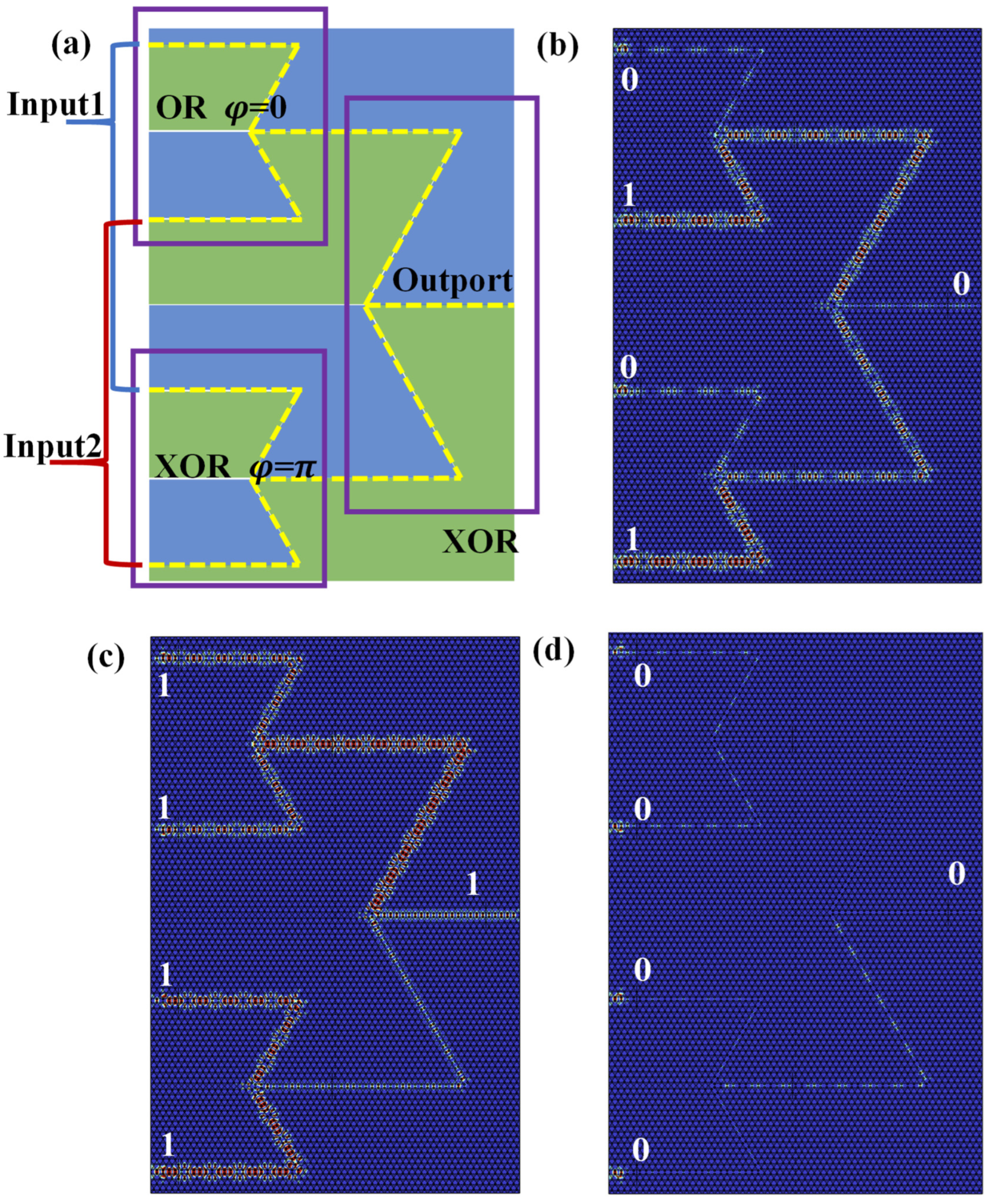
Figure 6.
AND gate (a) Normalized output power for different logic states versus frequency. (b) Extinction ratio for logic "1" and logic "0" outputs.
Figure 6.
AND gate (a) Normalized output power for different logic states versus frequency. (b) Extinction ratio for logic "1" and logic "0" outputs.


Table 1.
The truth table of XOR and OR gates.
| InputA (Port1) |
InputB (Port3) |
Output(Port4) OR XOR |
Transmittance OR XOR |
| 1 | 1 | 1 0 | 1.191 0.006 |
| 0 | 0 | 0 0 | 0.008 0.014 |
| 1 | 0 | 1 1 | 0.962 0.923 |
| 0 | 1 | 1 1 | 0.914 0.914 |
Table 2.
The truth table of AND gates.
| In1 In2 (OR XOR) |
Output(Port4) OR XOR AND |
Transmittance OR XOR AND |
|
| 1 | 1 | 1 0 1 | 1.323 0.018 0.717 |
| 0 | 0 | 0 0 0 | 0.058 0.009 0.043 |
| 1 | 0 | 1 1 0 | 0.925 0.883 0.054 |
| 0 | 1 | 1 1 0 | 0.913 0.954 0.027 |
Disclaimer/Publisher’s Note: The statements, opinions and data contained in all publications are solely those of the individual author(s) and contributor(s) and not of MDPI and/or the editor(s). MDPI and/or the editor(s) disclaim responsibility for any injury to people or property resulting from any ideas, methods, instructions or products referred to in the content. |
© 2026 by the authors. Licensee MDPI, Basel, Switzerland. This article is an open access article distributed under the terms and conditions of the Creative Commons Attribution (CC BY) license (http://creativecommons.org/licenses/by/4.0/).
Copyright: This open access article is published under a Creative Commons CC BY 4.0 license, which permit the free download, distribution, and reuse, provided that the author and preprint are cited in any reuse.