

Submitted:
28 May 2026
Posted:
29 May 2026
You are already at the latest version
Abstract
Modern optoelectronic devices, such as light-emitting diodes and laser diodes, rely on nitride-based (GaN, AlN, InN) quantum structures, which underpin current technologies. These systems enable emission across a broad spectral range—from ultraviolet to infrared—with properties tunable via composition, strain, and quantum confinement. This review summarizes progress in the performance of nitride emitters across the full spectral range, with particular emphasis on the evolution of external quantum efficiency (EQE). Nitride emitters are primarily based on InGaN quantum wells, while AlGaN quantum wells are used for ultraviolet operation. Device performance is governed by the intrinsic properties of these structures, which also determine key physical challenges across different wavelength regions. Blue InGaN LEDs achieve the highest efficiencies (~60-80% EQE), while green devices are limited to ~20-35% due to the “green gap,” with further reduction (~5-20%) toward longer wavelengths. In the ultraviolet, AlGaN-based emitters exhibit lower performance due to material and structural challenges, although steady progress is being made. Special attention is given to mechanisms limiting EQE, including efficiency droop in the green-red region, and ongoing efforts to mitigate these effects. Finally, perspectives for future applications of nitride-based quantum structures in optoelectronics are outlined.
Keywords:
nitride quantum structures
; InGaN
; AlGaN
; external quantum efficiency
; light-emitting diodes
; laser diodes
; optoelectronics
1. Introduction
Nitride-based quantum structures (QSs) form the foundation of optoelectronic devices such as light-emitting diodes (LEDs) and laser diodes (LDs), operating across a broad spectral range from the ultraviolet (UV) to the infrared (IR). Their emission properties can be engineered through the choice of quantum-structure type, composition, and material design.
Most semiconductor light emitters are based on III-V compounds; however, conventional arsenide- and phosphide-based systems are limited in achieving sufficiently wide band gaps for efficient emission in the green-blue spectral range. Although alloying materials such as GaAs with Al or P increases the band gap, these alloys tend to become indirect beyond certain compositions, significantly reducing radiative efficiency. Consequently, these systems are largely restricted to the red and part of the yellow spectral range.
To reach higher photon energies, wide-band gap II-VI semiconductors, particularly Zn-based compounds, have been extensively investigated. While these materials enable blue-green emission and even lasing, their practical use is limited by very short device lifetimes.
In contrast, GaN and its alloys with In (InGaN) and Al (AlGaN) offer a much wider band-gap range, enabling emission from the deep UV to the near IR. InGaN-based LEDs and LDs cover the visible spectrum, particularly the blue-green region, while AlGaN-based structures extend operation into the UV. This wide tunability makes the III-nitride system uniquely versatile for both incoherent and coherent light sources. Nowadays, III-nitride semiconductors constitute one of the most important material systems in modern optoelectronics. Quantum wells based on III-nitride materials form the active region of LEDs and LDs, which underpin solid-state lighting, display technologies, and a wide range of emerging photonic applications. Figure 1 schematically illustrates the spectral range accessible with nitride-based quantum structures.
For over three decades, research on III-nitrides has focused on improving luminous efficiency, initially targeting high-efficiency blue emission and later extending across the visible spectrum [1,2]. Progress has been driven by advances in epitaxial growth, doping, and defect reduction, as well as by the transition from large-area LEDs to low dimensional structures, as micro- and nano-LEDs.
The development of visible-light LEDs has transformed modern lighting, especially through white sources based on blue InGaN emission with phosphors like YAG:Ce. Now exceeding 10 billion units annually, LED bulbs have largely replaced incandescent lighting, significantly reducing energy consumption. Their impact comes from high luminous efficacy (>150 lm/W, up to 250 lm/W [3]), along with easy control, smart-system compatibility, and tunable color temperatures. White LEDs are widely used for backlighting in displays (monitors, TVs, and mobile devices), reaching several billion units annually, and are also key in automotive lighting (headlights, daytime running lights, and interiors). High-power red, amber, and green LEDs are essential for traffic signals and large-scale signaling systems. Blue and green LEDs underpin display technologies (RGB and microLED) and architectural lighting, while blue LEDs additionally enable white light via phosphors and are used in communication, medical illumination, and fluorescence sensing.
UV LEDs further broaden applications: UVA (320-400 nm) are used in curing, fluorescence detection, and 3D printing; UVB (280-320 nm) in specialized medical treatments such as phototherapy; and UVC (200-280 nm) in disinfection of water, air, and surfaces by inactivating microorganisms through DNA and RNA damage. Although LEDs dominate the market, LDs remain essential due to their high coherence and high optical power density. In the UV–blue spectral range, nitride-based LDs were historically used in optical data storage systems (e.g., Blu-ray Disc) and are currently applied in digital printing, high-resolution projection systems, and advanced RGB displays.
Green LDs are particularly important for laser projection, AR/VR systems, and high-brightness displays, enabling wide color gamut and high efficiency. Their use also extends to spectroscopy, biomedical applications, and optical metrology, where directional, monochromatic light is required.
Despite progress toward longer wavelengths, efficient red-emitting nitride LDs have not been reproducibly achieved. This is mainly due to material challenges, including the high indium content required, which degrades crystal quality, enhances internal electric fields, and reduces electron-hole overlap. As a result, red laser diodes are typically based on alternative systems such as AlGaInP.
Nitride light emitters are based on QSs, including layered systems and low-dimensional forms such as nanowires and quantum dots (QDs).
Layered QSs comprise single and multi quantum wells (SQWs, MQWs) and superlattices (SLs), with properties determined by layer thickness and crystallographic orientation. MQWs consist of isolated QWs separated by thick barriers, whereas SLs are formed by thin, strongly coupled layers, leading to wavefunction overlap and miniband formation. Thus, SLs can be regarded as short-period MQWs with strong inter-well coupling.
Low-dimensional structures such as micro-/nanostructures, QDs, and nanowires are promising for LEDs and LDs due to suppressed internal electric fields, reduced defect densities, and enhanced indium incorporation. Nanowires support efficient carrier transport, while QDs, with discrete energy levels, exhibit size-dependent emission. Nitride QDs offer strain relaxation, reduced confinement [4], strong carrier localization that suppresses nonradiative recombination [5,6], large exciton binding energies [7,8], high thermal stability and potential mitigation of efficiency droop and the green gap [9,10]. However, their properties are highly size-dependent, and their quantum efficiency is typically lower than that of MQWs. The growth of InGaN QDs remains challenging due to thermal instability, often limiting room-temperature (RT) emission. Nevertheless, single QDs or nanowires can act as single-photon emitters and are also used in larger-scale devices (e.g., as QD layers), combining micro- and macro-scale features.
Nitride light emitters are mainly based on InGaN QWs, with AlGaN QWs used for UV emission, and their performance is governed by intrinsic material properties. We start the review with blue InGaN emitters, historically the first and still the most efficient. Toward shorter wavelengths, UV AlGaN emitters remain less efficient due to material limitations, although continuous progress is being made. Next, we move from blue toward the green-red spectral range, where efficiency decreases because of difficulties in growing high-quality, high-indium InGaN QWs. Nevertheless, recent advances in high-In-content InGaN have brought efficient red emission closer to realization, supporting the development of monolithic RGB devices. The review concludes by outlining future directions, including new concepts and emerging systems such as h-BN and hybrid nitride/oxide heterostructures.
2. Quantum Wells in Nitride Light Emitters
From a physics perspective, nitride devices remain challenging due to complex material properties. Although the general concept of QWs in nitride emitters is like that in GaInAsP systems, important differences arise. Nitride semiconductors have a hexagonal wurtzite (WZ) structure without inversion symmetry, which together with strong bond iconicity leads to significant spontaneous and piezoelectric polarization [11,12].
2.1. Quantum confined Stark Effect
In InGaN/GaN QWs, differences in composition and strain between compressively strained InGaN and nearly strain-free GaN generate polarization discontinuities at the heterointerfaces. These discontinuities induce fixed interface charges and strong internal electric fields, which tilt the conduction and valence band edges and spatially separate electron and hole wave functions, giving rise to the quantum-confined Stark effect (QCSE). QCSE is a characteristic feature of wurtzite (WZ) QSs and strongly influences their optical properties. Figure 2a schematically illustrates the QCSE, while Figure 2b presents its impact on the electronic band structure through calculated band profiles of InGaN/GaN MQWs.
QCSE is not unique to III-N semiconductors; it also occurs in GaAs/InGaAs structures grown along the (111) direction [13], though much more weakly, whereas in InGaN QWs internal fields can reach 1-3 MV/cm [14]. It modifies optical properties by increasing carrier lifetimes (from sub-ns to tens or hundreds of ns [15]) and causing a redshift of emission. As a result, emission depends not only on composition but also on well width and polarization differences, with recombination resembling spatially indirect donor-acceptor pair transitions.
The QCSE has long been considered detrimental to device efficiency, since the optical transition matrix element is proportional to the electron-hole wavefunction overlap:
where uc, uv are Bloch functions and Ψe,Ψh are electron and hole wavefunctions. The radiative efficiency is given by:
Thus, τr≪τnr would suggest low efficiency. However, despite long recombination times in InGaN QWs, high radiative efficiency is observed. This apparent paradox was resolved around 2013 by Kioupakis et al. [16], who showed that both radiative and nonradiative recombination rates are similarly affected by the internal electric field associated with QCSE.
Experimental studies (e.g., Marona et al. [15])) confirmed that both τr and τnr increase with increasing field. Nevertheless, the reduced overlap Mcv remains detrimental for LDs, since the optical gain is proportional to ∣Mcv∣2. As the electron-hole wavefunction overlap decreases, the optical gain is reduced, which is critical because the gain must overcome resonator losses for lasing to occur [17]. To mitigate the QCSE, two main strategies are used: growth of QWs on nonpolar or semipolar crystallographic planes, and engineering of staggered QW structures to enhance carrier overlap.
2.2. Nonpolar and Semipolar Crystallographic Planes
In WZ nitrides, polarization discontinuity strongly depends on crystal orientation, ranging from fully polar c-plane (0°) to nonpolar m-plane (90°). Semipolar orientations have been widely studied, notably by the University of California, Santa Barbara group [18] demonstrating promising device performance. However, their practical use is limited by high oxygen incorporation during growth [18,19], strain relaxation via dislocation formation [19], and the limited availability of large-area (≥2-inch) substrates
2.2.1. Staggered QWs
An alternative approach is quantum well (QW) engineering to enhance electron-hole overlap using staggered QWs. These structures consist of ultrathin layers forming shallow and deep potential wells, in various configurations (Figure 3). In staggered InGaN QWs, the overlap integral can increase by up to a factor of two, significantly reducing the QCSE. Such designs are widely used, although their implementation depends on the overall LED or LD architecture.
A key challenge of InGaN QWs is achieving pseudomorphic growth at high indium content due to the large lattice mismatch (~11.6%) between GaN and InN. As indium incorporation increases, strain energy rises, leading to “composition pulling” [20,21], which limits further incorporation. Above ~27% In, growth tends to become three-dimensional, hindering pseudomorphic layers [22]. Even a monolayer of InN on GaN yields only ~30% average incorporation [23,24], highlighting strong strain constraints. These effects are also linked to spinodal decomposition and Stranski-Krastanov growth instability [25]. Approaches to mitigate this include relaxed InGaN buffers [26] and compliant templates such as porous GaN [27].
2.3. Sources of Nonradiative Recombination
Since most nitride LEDs are grown on sapphire, they exhibit high threading dislocation densities (~108-109 cm-2). While such defects would typically reduce radiative efficiency, InGaN devices remain highly efficient. This paradox was first addressed by Chichibu [28], who attributed it to carrier localization in potential minima caused by compositional fluctuations, limiting diffusion to dislocations. However, reported long carrier diffusion lengths (μm scale) [29,30] are not fully consistent with this model.
An alternative explanation by Hangleiter [31] suggests that threading dislocations form V-shaped pits with sidewall QWs of higher effective band gap, creating barriers that prevent carrier capture and account for both high efficiency and long-range transport. In addition to extended defects such as dislocations, intrinsic nonradiative processes also strongly affect InGaN QW efficiency. A key issue is the “efficiency droop” in InGaN LEDs [32], i.e., reduced radiative efficiency at high current densities. Initially attributed to electron leakage into p-type layers [32], it is now mainly linked to Auger recombination in the QWs [33]. The relatively low probability of conventional Auger recombination in wide-bandgap semiconductors has led to the proposal of alternative mechanisms, including phonon-assisted and disorder-enhanced Auger processes [34]. From the perspective of radiative efficiency, particularly at low current densities, Shockley–Read–Hall (SRH) recombination through defect states is the dominant nonradiative recombination mechanism.
2.4. AlxGa1-xN/AlyGa1-yN and AlInGaN/AlGaN QWs for UV Emitters
Since the bandgap of GaN at RT corresponds to ~365 nm emission, shorter-wavelength emitters require AlGaN or quaternary AlInGaN. AlGaN can be grown over the full composition range without phase separation [37], but unlike InGaN, its radiative efficiency is more sensitive to dislocation density—a trend also observed in low-In-content InGaN [38]. In InGaN/GaN QWs, strong piezoelectric polarization generates internal fields of ~1-3 MV/cm, causing pronounced QCSE and reduced electron-hole overlap. In contrast, AlGaN/AlGaN QWs have smaller lattice mismatch, leading to weaker piezoelectric effects and a relatively larger role of spontaneous polarization. Thus, polarization balance in AlGaN structures is more sensitive to composition and strain. While both systems exhibit strong polarization effects, InGaN/GaN is typically piezoelectric effect-dominated, whereas in AlGaN/GaN the spontaneous and piezoelectric contributions are more comparable [39,40]. The valence band in WZ nitrides consists of three subbands: heavy hole (Γ9), light hole (Γ7), and crystal-field split-off hole (Γ7) (see Figure 4).
In AlxGa1-xN alloys, increasing Al content causes valence band reordering due to competition between crystal-field splitting (Δcf) and spin-orbit interaction (Δso). In GaN (Δcf > 0), the top valence band is Γ9 (HH), while in AlN (Δcf < 0) it is Γ7 (CH). The transition occurs at x ≈ 0.6-0.7 (strain-dependent).
This inversion changes the emission character from TE to TM polarization. In c-plane devices, TM light is emitted along the growth direction and is poorly extracted, reducing efficiency. It also alters transition matrix elements, lowering radiative recombination—an effect particularly important for deep-UV AlGaN emitters [41,42].
3. Nitride Light Emitters: From Blue to Ultraviolet (500-200)
LED and LD epitaxial structures differ fundamentally in both complexity and operation. InGaN-based LEDs typically employ relatively simple InGaN/GaN MQW structures designed for spontaneous emission over a broad area, without the need for optical confinement or a resonant cavity. In contrast, blue LDs require carefully engineered QWs, waveguides, cladding layers, and current confinement structures to achieve stimulated emission and optical gain. Consequently, their epitaxial structures are significantly more complex.
A standard GaN-based blue LED typically consists of a sapphire or Si substrate, a GaN buffer layer to improve crystal quality, an n-type GaN layer, an InGaN/GaN MQW active region where radiative recombination occurs and light is generated, an AlGaN electron-blocking layer (EBL) that prevents electron leakage from the QWs, a p-type GaN layer, and a heavily doped p-type GaN contact layer.
A standard GaN-based blue/violet LD typically consists of a sapphire substrate, or GaN in modern devices, n-AlGaN cladding layer, lower InGaN waveguide, MQW active region (usually 2-4 InGaN QWs), upper InGaN waveguide, AlGaN EBL, p-AlGaN cladding layer, and a heavily doped p-type contact layer. Together, these layers provide efficient carrier and optical confinement as well as stimulated recombination within the QWs.
Figure 5 schematically compares the epitaxial structures of a typical InGaN-based blue (a) LED and (b) laser diode (LD). The general device architecture is broadly applicable to most nitride light emitters. Across the visible spectral range, active regions are typically based on InGaN QWs, whereas AlGaN QWs are commonly employed for UV emission. The main differences between individual devices arise from variations in layer composition and structural design optimized for specific operating wavelengths and device requirements.
In the following, LEDs and LDs operating across successive spectral ranges are briefly described, with particular attention to the quantum structures forming the active region and to the external quantum efficiency (EQE) of the devices. EQE is defined as the product of the internal quantum efficiency (IQE) and the light-extraction efficiency (ηext):
3)
where ηext denotes the fraction of internally generated photons that escape from the device. Consequently, EQE is always lower than IQE due to optical losses such as absorption, reflection, and waveguiding. For both LEDs and LDs, EQE describes the efficiency of converting injected carriers into emitted photons. In LEDs, emission arises from spontaneous recombination, whereas in LDs stimulated emission dominates above threshold. Thus, LED EQE reflects overall radiative and extraction efficiency, while LD EQE is more closely related to slope efficiency and cavity losses and is commonly expressed as the differential EQE.
3.1. Blue-violet (500-400)
3.1.1. LEDs
In 1994, following the growth of high-quality InGaN films, Nakamura and coworkers [43] demonstrated candela-class, high-brightness InGaN/AlGaN blue LEDs suitable for commercial applications, with luminous intensities exceeding 1 cd. The active region consisted of a Zn-doped InGaN/GaN MQW. The devices exhibited a typical output power of ~1.5 mW and EQE of up to 2.7% at a forward current of 20 mA under RT operation.
In the same year Nakamura et al. [44] fabricated SQW LEDs emitting in the blue to green spectral range. The active region consisted of a single 2 nm thick InGaN/GaN QW. The blue LEDs exhibited an output power of 4 mW at a drive current of 30 mA and an EQE of 2.4% at 20 mA under RT operation. The electroluminescence (EL) peak was centered at 500 nm.
Following the initial demonstrations of InGaN/GaN blue LEDs development in the 400-500 nm range rapidly progressed from proof-of-concept devices to highly efficient commercial LEDs. In the early 2000s, optimization of MQW active regions, barrier design, strain engineering, and light extraction enabled blue LEDs with EQEs exceeding 30-40%, later surpassing 50% in commercial devices.
Narukawa et al. [45,46,47] fabricated high-luminous-efficiency white LEDs using high-efficiency blue LEDs and YAG phosphors. The reported blue devices exhibited output powers of 47.1 and 42.2 mW with EQEs of 84.3% and 75.5%, respectively. The efficiency improvement was attributed to: (i) highly transparent indium tin oxide (ITO) electrodes (>95% transmittance at 450 nm), which serve as transparent p-type contact layers enabling uniform current injection while minimizing optical absorption, and (ii) patterned sapphire substrate (PSS) that enhance light extraction by reducing total internal reflection within the nitride layers. It indicates that simultaneous optimization of IQE and light extraction is essential for achieving very high EQE.
Parallel advances in microLED technology further exploited the high internal efficiency of InGaN, enabling efficient emitters for displays and visible-light communication. Collectively, these developments established III-V nitrides as the dominant material system for blue and violet light emitters.
Hurni et al. [48] reported violet-emitting III-nitride LEDs grown on bulk GaN substrates, employing a triangular volumetric flip-chip architecture. The device performance is optimized for operation at high current densities and elevated temperatures through specific design considerations for the epitaxial layers, light extraction efficiency, and electrical injection. They demonstrated that the use of bulk GaN substrates systematically enables improved performance over standard LED technology, including superior IQE, EQE, and electrical efficiency. The EQE reaches 80% at a wavelength of 415 nm.
Li et al. [49] demonstrated cascaded blue/green micro-LEDs with independently controlled junctions, grown by metal-organic chemical vapor deposition (MOCVD). The devices integrate blue μLEDs, a tunnel junction, and green μLEDs, enabling independent blue, green, and combined emission. The blue (60×60 μm2) μLEDs exhibit forward voltage of 4.1 V at 20 A/cm², with peak EQEs of 42%. The emission peak is located at 518 nm, with FWHM value of 19. These results demonstrate the potential of cascaded LEDs for monolithic full-color integration. Sheen et al. [50] demonstrated blue InGaN nano-LEDs with an EQE of 20.2 ± 0.6% at ~440 nm using sol-gel SiO2 surface passivation, which reduced surface recombination by passivating GaN dangling bonds.
Higher EQE values have been reported recently. Choi et al. [51] in 2024 investigated efficiency droop in blue and green GaN-based LEDs and LDs using identical epitaxial structures with different indium contents. The active region consisted of 2.0 nm InGaN QWs separated by 7.5 nm InGaN QBs. For the blue devices, the QWs contained 15% In, while the QBs contained 2% In. The resulting emission wavelengths were 430 nm for LEDs and 440 nm for LDs, with corresponding EQE values at 25 mA of approximately 91.9% and 44.7%, respectively.
3.1.2. LDs
The first nitride-based LDs were demonstrated in 1996 by Shuji Nakamura and co-workers [52], emitting at 417 nm. The devices were grown by MOVPE on sapphire substrates with an n-type GaN buffer layer to accommodate lattice mismatch. The structure included n-type In0.1Ga0.9N, n-type Al0.15Ga0.85N, and n-type GaN layers for carrier injection and optical confinement. The active region consisted of 26 In0.2Ga0.8N/In0.05Ga0.95N MQWs, followed by a p-type Al0.2Ga0.8N EBL and p-type GaN layers for hole injection and contacts (see Figure 6). Lasing was achieved at a relatively high operating voltage (~30 V), which prevented CW operation.
Later in 1996, Nakamura’s group achieved the first CW operation of a violet InGaN LD [53]. Although the initial device operated for only about one second, the threshold voltage was reduced to 8 V. By the end of the year, further optimization extended device lifetime to 27 hours, lowered the voltage to 5.5 V, and maintained a threshold current density of ~3.6 kA/cm². Subsequent design improvements led to the introduction of ridge geometry later that year, reducing the voltage to 20 V, the threshold current density to 3 kA/cm², and the number of QWs to five. Continued progress in 1997 increased the lifetime to approximately 300 hours.
In general, blue LDs exhibit EQEs than blue LEDs. Modern blue LDs typically achieve EQEs of ~20-45%, compared to peak values of ~80-90% for blue LEDs. This difference arises from the greater sensitivity of LDs to crystal defects, stronger Auger recombination at the high current densities required for lasing, carrier leakage from quantum wells, optical losses in waveguides and cavity mirrors, and the influence of polarization-induced electric fields in c-plane InGaN structures. Although LDs operate with smaller emission areas and therefore at much higher current densities, these conditions do not improve peak EQE; instead, they contribute to additional efficiency losses.
Following the successful development of InGaN-based blue–violet LEDs and LDs, research quickly shifted toward shorter wavelengths using AlGaN-based QWs, extending nitride emission into the UV region. UV optoelectronic devices are typically based on AlGaN heterostructures. UV emitters are commonly classified as UVA (400-315 nm), UVB (315-280 nm), and UVC (280-200 nm), with their applications largely determined by photon energy and the corresponding interaction mechanisms with biological and chemical systems.
3.2. UVA (400-315 nm)
UVA emitters are widely used in photopolymerization and fluorescence excitation, with applications ranging from UV curing and 3D printing to microscopy, diagnostics, insect traps, and phosphor pumping for white light. Their lower photon energy and deeper penetration make them suitable for photochemical processes with reduced biological risk compared to shorter UV wavelengths.
3.2.1. LEDs
The first UV LED, emitting at 375 nm, was reported by Akasaki et al. [54] in 1993, with an EQE of 1.5%. It was grown using MOVPE and hydride vapor phase epitaxy (HVPE) on a highly mismatched substrate. This approach enabled the growth of high-quality nitride films on substrates such as α-Al2O3. Next, Mukai et al. [55] in 1998 achieved 7.5% EQE at 371 nm using the InGaN/AlGaN double heterostructure with an In composition of nearly zero. The undoped GaN layer acts as a buffer to reduce lattice mismatch, a diffusion barrier, and a stress-relief layer, thereby improving device performance and reliability. Progress continued Muramoto et al. [56] demonstrating EQEs up to 60% due to advances in crystal growth, chip processing, and packaging technologies. Later work by Tak Oh et al. [57] showed that optimized AlN nucleation layers reduce defects and enhance EQE. The EQE at 370 nm was 43.7% for in situ AlGaN and 48.2% for ex situ AlN. Designing efficient UV LEDs is challenging due to AlGaN material defects, low hole concentration, poor p-type contacts, limited light extraction, polarization-induced losses, and thermal issues. To overcome these limitations, significant research efforts have been directed toward improving crystal quality and optimizing device architectures, including the implementation of patterned substrates and distributed Bragg reflector (DBR)-based resonant cavity LED (RCLED) designs [58]. For example, Lu et al. [59] demonstrated a 365 nm UVA LED incorporating nanoporous AlGaN DBRs with a reflectance of 93.5%. This design increased the EQE by ~54% and the output power by ~66% without degrading electrical performance, highlighting the strong potential of DBRs for enhancing light extraction in LEDs. However, the use of RC LEDs remains relatively limited.
In 2020, Li et al. [60] demonstrated high-efficiency 395 nm UVA LEDs grown on Si substrates using InGaN/GaN/AlGaN/GaN MQWs. A GaN interlayer barrier improved carrier concentration and overlap by tuning band structure and polarization effects, while also enhancing crystal quality through a two-step growth process. The resulting devices achieved 60% EQE and 659 mW output power at 350 mA injection current. The structure is illustrated in Figure 7.
3.2.2. LDs
Early UVA LDs based on AlGaN and AlInGaN MQWs, typically grown on sapphire, exhibited high threshold current densities and were largely limited to pulsed operation. Their performance was constrained by high dislocation densities, inefficient p-type doping in Al-rich materials, and strong internal electric fields.
A review by Yang et al. [61] outlines key strategies for improving GaN-based UVA LDs (320-400 nm), including high-quality crack-free AlGaN templates, optimized active regions and waveguides, and improved thermal management. In 2003, Masui et al. [62] demonstrated CW operation at 365 nm with a 50 mA threshold current and ~2000 h lifetime. Later, Yoshida et al. [63,64] achieved AlGaN MQW LD emission at 342.3 and 336.0 nm, demonstrating the potential of AlGaN-based LDs for shorter-wavelength UV operation.
Taketomi et al. [65] demonstrated high-peak-power operation of an AlGaN-based UVA LD emitting at 338.6 nm. The device was fabricated on a bulk GaN(0001) substrate using a crack-free Al0.3Ga0.7N underlying layer grown by epitaxial lateral overgrowth (ELO). A broad-area, vertically conductive structure was employed to enhance output power. The device exhibited a threshold current density of 38.9 kA/cm2 and a differential EQE of 8.5%, with a characteristic temperature of 119 K and a wavelength temperature coefficient of 0.033 nm·K-1. A peak output power exceeding 1 W was achieved under pulsed operation at RT, representing one of the highest reported values until 2022. The schematic of their epitaxial structure is shown in Figure 8.
Zhao et al. [66] demonstrated CW GaN-based UV laser diodes in 2017, achieving emission at 392.9 and 381.9 nm with output powers of 80 mW and 14 mW, respectively. Yang et al. [67,68,69,70] showed that waveguide thickness plays a critical role in UV LD performance: thinner layers reduce carrier loss and threshold current, whereas excessively thin designs increase optical leakage. Optimized structures enabled emission down to ~358 nm and CW output powers up to 3.8 W at ~386 nm with wall-plug efficiencies approaching 20%.
Commercially, Nichia Corporation has developed GaN-based LDs operating in the 375-380 nm range with stable CW operation, high output power, and long lifetime for applications such as optical storage and biomedical sensing [71].
3.3. UVB (315-280 nm)
UVB emitters are mainly applied in medical phototherapy, vitamin D synthesis, dermatological treatment, and biological and environmental research. UVB radiation induces controlled photochemical and biological responses, enabling therapeutic applications while avoiding the extreme DNA damage efficiency characteristic of UVC radiation.
In the early 2000s, fabricating UV LEDs with wavelengths below 300 nm was highly challenging due to the need for wide bandgap materials, which were scarce, difficult to process, and prone to absorption and scattering losses, resulting in low efficiency.
3.3.1. LEDs
The first sub-300 nm UVB LEDs were developed in 2000 by Nitride Semiconductor Co. in collaboration with the University of Tokushima (see the review by Muramoto et al. [56]). In 2009, Hirayama et al. [72] achieved 1.2% EQE at 282 nm using LEDs grown on low threading-dislocation AlN templates fabricated by an NH₃ pulse-flow multilayer technique. The devices included 222-273 nm Al0.83-0.89Ga0.17-0.11N/Al0.47-0.67Ga0.83-0.89N -based LEDs and >280 nm InAlGaN-based LEDs with high Al content. In 2010, Shur et al. [73] demonstrated a GaN-based UV LED with an efficiency of 0.01% at wavelengths below 300 nm and Fujioka et al. [74] improved the efficiency of 280 nm UV LEDs to approximately 2.78%. This was achieved by employing high-crystal-quality AlN templates with optimized epitaxial structures.
Significant progress in UVB LED performance was reported by Khan et al. [75] in 2020, who demonstrated AlGaN-based LEDs emitting at 310 and 294 nm through optimized carrier transport and MQW design. The 310 nm device achieved 29 mW output power and 4.7% EQE, while the 294 nm LED with increased Al content in the undoped AlGaN layer, reached 32 mW and 6.5% EQE under pulsed operation at RT. Further improvements were reported by the same authors in 2025 [76], with EQE reaching 9.6% for for 304 nm AlGaN-based UVB LEDs. The enhancement resulted from improved light extraction using nano-patterned sapphire substrates, photonic crystals, and Al reflectors.
In 2023, Wang et al. [77] investigated challenges in growing highly conductive n-AlGaN layers for germicidal UV (GUV) LEDs. They showed that thick, heavily Si-doped n-AlGaN suffers from surface degradation caused by the Si antisurfactant effect, resulting in dislocation inclination, strain relaxation, cracking above 400 nm thickness, and unintended Ga incorporation. By optimizing the n-AlGaN conductivity and using thinner conductive layers with a smoothing SL, they demonstrated 285 nm UV LEDs with a low forward voltage of 4.2 V and a peak EQE of 10.6%.
At the same time, several groups reported UV-emitting micro- and nano-LEDs suitable for high-performance displays due to their high efficiency, brightness, and stability. However, in these and similar studies, EQE decreases with device size and remains lower than in conventional MQW structures, dropping from ~10% for ~10 μm devices to ~2–3% at ~1 μm [78]. Zhao et al. [79] fabricated AlGaN-based micro-ring LEDs and showed that optimized ring geometries improve optical emission and light extraction efficiency compared with conventional micro-circular LEDs. Their best device, emitting at ~280 nm, achieved a light output power density of 53.36 W/cm2 at 650 A/cm2 and an EQE of 6.17%, demonstrating the potential of ring-shaped micro-LEDs for enhanced UV emission.
3.3.2. LDs
The first electrically pumped AlGaN-based thin-film laser operating below 300 nm was demonstrated by Zhang et al. [80] thanks to the use of polarization doping, in 2019 at 271.8 nm, followed by RT pulsed UVB lasers emitting at 298 nm (Sato et al. [81]). Subsequent improvements in 298 nm laser performance were reported by Omori et al. [82], while electrically pumped 310 nm UVB lasers were demonstrated in 2021 by Hjort et al. [83].
3.4. UVC (280-200)
UVC nitride emitters are primarily used for disinfection and sterilization in medical equipment, wastewater treatment, air purification, and food and packaging sterilization. Their effectiveness arises from the high photon energy, which directly damages microbial nucleic acids, leading to efficient inactivation of bacteria, viruses, and other pathogens.
3.4.1. LEDs
In 2012, Shatalov et al. [84] enhanced the performance of AlGaN-based UVC LEDs grown on sapphire substrates by optimizing chip encapsulation. As a result, they achieved an EQE of 10.4% at 20 mA CW operation, with output power up to 9.3 mW at 278 nm. Hirayama et al. [85] (2014) reported AlGaN-based DUV LEDs operating from 222 to 351 nm. Improved crystal growth, low-TDD AlN buffers, MQB structures, and enhanced light extraction enabled a maximum EQE of 7% at 279 nm.
Bryan et al. [86] studied Al0.55Ga0.45N and Al0.55Ga0.45N/Al0.85Ga0.15N -based UVC MQWs grown on bulk AlN substrates and achieved a record IQE of ~80% at 258 nm under high V/III growth conditions, attributed to reduced nonradiative recombination and improved MQW quality. To improve EQE, Takano et al. [87] employed a transparent Al0.65Ga0.35N:Mg contact layer, a Rh mirror electrode, growth on an AlN template over patterned sapphire, and resin encapsulation. Significantly enhanced light extraction resulted in a maximum EQE of 20.3% at 275 nm. Maeda et al. [88] achieved 9% EQE at 279 nm using transparent contact layers and reflective Ni/Al p-electrodes. An optimal Ni thickness of ~0.9 nm provided the best balance between reflectivity and efficiency.
In 2020, Pandey et al. [89] investigated LEDs operating near 265 nm and achieved an EQE of 11% using an AlGaN/GaN/AlGaN tunnel-junction structure. A thin GaN layer inserted between p+- and n+-AlGaN layers reduced the tunneling barrier and improved carrier injection. In 2021, Zheng et al. [90] reported 5.19% EQE at 273 nm using a double-layer nano-patterned array that improved light extraction by diffraction and reduced absorption.
Matsukura et al. [91] studied how the optical thickness of p-layers affects light output in AlGaN-based deep-UV LEDs with transparent high-Al-content p-AlGaN cladding, a thin p-GaN contact layer, and a reflective p-electrode. Maximum output was obtained when the total p-layer optical thickness was ~0.66λ. At 275 nm, optimized devices achieved 385 mW output power at 1500 mA, a peak EQE of 15.7%, and a maximum wall-plug efficiency of 15.3% at 10 mA. The LEDs retained 85% of initial output after 1000 h, showing that optimizing p-layer optical thickness is crucial for improving light extraction.
Liu et al. [92] (2024) improved 270-nm AlGaN-based DUV LEDs using optimized MQWs, a reflective Al mirror, a low-loss tunneling junction, and a SiO2 insertion layer. The devices achieved 140.1 mW output power at 850 mA and an EQE of ~6.9%, while reducing QCSE, p-layer absorption, and poor TM-polarized light extraction.
Many other studies in the UVC spectral region have been carried out based on QDs. Among these, Yang et al. [93] demonstrated MOVPE-grown GaN/AlN QD LEDs emitting at 309 nm with stable emission up to 300 K and IQE of ~62% at RT. Brault et al. [94] reported MBE-grown AlᵧGa₁₋ᵧN QDs emitting between 332 and 276 nm having the low-temperature IQE up to 66%. Stachurski et al. [95] confirmed strong RT emission and exciton confinement in GaN/AlN QDs, while Zaiter et al. [96] achieved strong UV-C emission at 275-280 nm from MBE-grown Al0.3Ga0.7N QDs on ultrathin h-BN/sapphire templates.
3.4.2. LDs
Nitride emitters in the UVC range are currently limited mainly to LEDs, while LDs remain largely at the research stage due to significant material and device challenges.
Major advances in AlGaN-based LDs operating in the 200-280 nm range were reported by Zhang et al. [80,97,98] and Kushimoto et al. [99]. Key developments included high-quality AlGaN growth on single-crystal AlN substrates and improved p-type conductivity using distributed polarization doping. These advances enabled RT pulsed lasing and later CW operation at 5 °C through reduced dislocation density and optimized device design. CW lasing at 274.8 nm was achieved above 110 mA, with a threshold current density of 3.7 kA cm-2 and a low threshold voltage of 9.6 V using a double-sided n-electrode configuration.
Table 1 summarizes the performance of representative blue, violet, and UV LEDs and LDs discussed in this work, including emitter type and key characteristics, emission wavelength, EQE, and corresponding references.
- For LDs differential EQE is usually used.
Figure 9 shows the dependence of EQE on emission wavelength for the nitride light emitters listed in Table 1, illustrating the observed EQE trend. Figure 9 shows that InGaN-based blue LEDs achieve very high EQE (>70% at 440-450 nm) despite the high dislocation densities typical of heteroepitaxial III-nitride growth. This problem was discussed earlier in the text, but it’s still a question of a vigorous debate [100].
The lower EQE below 400 nm in the UVA region mainly results from the transition from InGaN/GaN to AlGaN/GaN material systems. Compared with InGaN, AlGaN exhibits weaker carrier and exciton localization, leading to enhanced nonradiative recombination. Poorer crystal quality, strain-related defects, and reduced optical confinement and light extraction further limit the quantum efficiency. In the UVC spectral range, the EQE tends to improve around 260–280 nm, likely due to the strong technological focus on this wavelength range, which is particularly important for disinfection applications. However, below ~ 280 nm (UVC range), the EQE decreases again because very high Al-content AlGaN suffers from poor crystal quality, inefficient p-type doping, and high defect densities. In addition, the emitted light becomes predominantly transverse magnetic (TM) polarized, causing more light to propagate parallel to the layers rather than out of the device, thereby reducing light-extraction efficiency.
A similar EQE wavelength dependence for blue to UV emitters, based on a broader dataset, was reported by Kneissl et al. [101]. A comparison of Figure 9 and Figure 5 in their work reveals the same overall trend. Efficiency improvement strategies in LEDs, highlighting progress driven by optimized device design, composition, and growth techniques were reviewed in 2024, by Battarai et al. [102].
4. Nitride Light Emitters: From Green to Red (500-750nm)
Red and green emitters are both essential for modern optoelectronic technologies, particularly in full-color displays, solid-state lighting, and laser-based systems. Along with blue emitters, they form the RGB platform necessary for a wide color gamut, high color fidelity, and brightness in LEDs, LDs, and emerging micro-LED displays. Green emission is especially important because the human eye is most sensitive in the green spectral region, making it critical for luminous efficiency, while red emission enables accurate color balance and extends functionality into sensing, communication, and biomedical applications.
4.1. Problems with Indium Content in InGaN QWs
Achieving high efficiency in the green-to-red spectral range remains challenging for III-nitride materials because longer wavelengths require higher indium incorporation in InGaN QWs. This increases strain, defects, compositional inhomogeneity, and QCSE, reducing radiative recombination efficiency. Lower growth temperatures and lattice mismatch further degrade material quality. These effects cause a strong efficiency drop toward the red region and are even more critical in LDs, where high material quality and optical gain are required, limiting the performance of green LDs and preventing practical red nitride-based LDs.
Yoshikawa [103] proposed an early strategy to improve long-wavelength III-nitride emitters by using binary InN/GaN SLs with ultrathin InN layers instead of high-In-content InxGa1-xN alloys placed in wide QWs. Since In-rich InGaN alloys tend to undergo phase separation and compositional fluctuations, the SL approach aimed to achieve better structural uniformity and more precise band-gap control while avoiding the limitations associated with high In incorporation.
Gorczyca et al. [104,105] predicted from ab initio calculations that the band gap in mInN/nGaN superlattices (SLs) decreases systematically with increasing InN and GaN layer thickness. A 1InN/15GaN SL was calculated to have a band gap of ~2.2 eV (~570 nm), in good agreement with the value reported by Miao et al. [106] (~2.17 eV for a 1InN/23GaN structure using multiband k·p modeling), suggesting the possibility of emission deep in the green spectral range. Extending these calculations over a broad range of SL periods revealed a continuous reduction of the band gap with increasing layer thickness. For sufficiently thick structures (m, n ≳ 6 monolayers), the band gap was predicted to close completely, indicating a polarization-induced semiconductor-to-metal transition driven by strong internal electric fields in the WZ structure. The calculated trends are illustrated in Figure 10.
However, fabrication of ideal InN/GaN SLs with 1-2 MLs of pure InN proved extremely difficult. Suski et al. [107] showed by high-resolution transmission electron microscopy (HRTEM) studies that nominal 1InN/GaN SLs actually contained InxGa1-xN layers with x ≈ 0.33 instead of pure InN. The measured PL energies agreed well with calculations for 1In0.33Ga0.67N/nGaN SLs (see Figure 10) highlighting both the promise of binary SLs for band-gap engineering and the practical limitations imposed by growth kinetics, interdiffusion, strain, and limited In incorporation in pseudomorphic InGaN/GaN QSs. Furthermore, it was recognized that limited indium incorporation, typically not exceeding approximately 30-33% is a general characteristic of all pseudomorphically grown InGaN/GaN QSs.
Duff al. [108] and Lymperakis et al. [109] showed theoretically that strong lattice-mismatch strain makes pseudomorphic InN growth on GaN energetically unfavorable, limiting stable In incorporation in coherent InGaN layers to about 25%. Their results also suggested that higher In incorporation could be achieved using In0.25Ga0.75N templates with reduced lattice mismatch, motivating the development of compositionally graded structures to alleviate strain effects. A few subsequent studies experimentally followed these suggestions [104,105,106].
Dussaigne et al. [110] used a relaxed InGaN pseudo-substrate to increase In incorporation and extend emission toward longer wavelengths. Reduced lattice mismatch lowered strain and compositional pulling effects, leading to strong PL redshifts compared with GaN substrates and enabling emission in the amber (~594 nm) and red (~624 nm) spectral regions.
Siekacz et al. [111] studied InGaN/GaN short-period SLs grown by plasma-assisted molecular beam epitaxy (PAMBE) on GaN and partially relaxed In0.2Ga0.8N buffer layers. PL measurements showed a systematic redshift of the emission peak with increasing in-plane lattice constant, from 379 nm for GaN substrates to 419 nm for In0.2Ga0.8N buffers. Staszczak et al. [112] performed similar studies on InGaN/GaN SLs grown by MOVPE on InGaN buffer layers with 17% and 20% In. A schematic diagram of such an SL structure is shown in Figure 11. Increasing the In content in the buffer to 20% significantly reduced the effective band gap, producing a redshift of about 0.72 eV (~167 nm) and extending the emission wavelength to ~590 nm in the amber spectral range.
The above experiments demonstrate that growth on relaxed InGaN buffers reduces lattice mismatch, enabling higher In incorporation in the InGaN QWs of the SL. Relaxed or partially relaxed InGaN buffer layers were subsequently adopted in various nitride light-emitting structures to facilitate longer-wavelength emission.
4.2. Green (500-590 nm)
4.2.1. LEDs
The first blue-green LEDs based on III-nitride semiconductors were demonstrated in the mid-1990s. In 1994, Shuji Nakamura and co-workers [44] reported blue-green LEDs exhibiting a luminous intensity of 2 cd. This performance was achieved by increasing the In composition in the InGaN active layer to 23% and by co-doping the layer with Zn and Si to optimize carrier concentration and radiative recombination efficiency. In a subsequent report published in 1995, Shuji Nakamura et al. [113] demonstrated super-bright green LEDs employing a p-AlGaN/InGaN/n-GaN heterostructure grown by MOCVD on sapphire substrates. These devices exhibited a luminous intensity of 12 cd and EQE 6.3% at a forward current of 20 mA, the output optical power was 3 mW and the EL peak wavelength was 520 nm.
After the initial demonstrations of green InGaN LEDs, major challenges remained in achieving higher efficiency and longer wavelengths. Further progress is fundamentally limited by strong polarization-induced electric fields that reduce radiative recombination. A common approach to suppress these fields is growth along semipolar or nonpolar directions, but practical implementation is hindered by growth complexity, limited In incorporation, and the lack of high-quality substrates. Other explored strategies include improving crystal quality, using AlGaN interlayers, pre-strained templates, and employing QDs or nanowires.
In 2018 Li et al. [114] in 2018 demonstrated InGaN-based green LEDs grown on c-plane patterned sapphire substrates using MOCVD. The 527 nm green LEDs exhibited a high EQE of 53.3%, a wall-plug efficiency (WPE) of 54.1%, and a peak luminous efficacy of 329 lm/W. Zhou et al. [115] systematically studied mechanisms for efficient green LEDs. Using cathodoluminescence and Raman measurements, they showed that V-pit induced potential barriers in InGaN/GaN structures suppress non-radiative recombination at threading dislocations, significantly improving IQE. The barrier height depends on V-pit diameter, influencing efficiency, forward voltage, and droop. Optimized V-pit structures enabled 525 nm green LEDs with an EQE of 42%.
Leem et al. [12] investigated the low efficiency of green LEDs using microscopic PL analysis of GaN-based InGaN/GaN MQWs. They found that In-enriched clusters, previously considered efficient emitters, actually localize excessive carriers and promote nonradiative recombination. Their formation through metastable phase separation also degrades the surrounding crystal quality, effectively reducing the active volume of the LED.
Lv et al. [116] reported 525 nm green LEDs with EQE up to 55.6%, using an optimized InGaN/GaN MQW structure grown on PSS by MOCVD. The device structure included an AlN buffer layer, a 3.3 µm thick n-type GaN layer, and 32 periods of InGaN/GaN SL for strain relief. Performance improvement was achieved by optimizing the thickness of the three inner QBs. The structure is illustrated in Figure 12.
Guo et al. [117] studied AlGaN interlayers in GaN-based green LEDs on silicon. The interlayers improve luminous efficiency by enhancing carrier distribution, suppressing dislocations, and reducing InGaN phase separation via increased compressive stress. They also strengthen V-pit effects. However, under electrical stress, they promote defect formation, causing light degradation at low current. The 525 nm LEDs achieved a peak EQE of 50%.
Choi et al. [51] investigated efficiency droop in blue and green GaN-based LEDs and LDs using epitaxial structures with varying indium content. For green emission, the In content in the QWs was 25%, while the QBs contained 2% indium, corresponding to an emission wavelength of 520 nm. The reported EQE was 78.8%.
Numerous other studies have explored strategies to improve green LED performance. Liu et al. [118] introduced V-pit embedded InGaN/GaN SLs that suppressed nonradiative recombination and enhanced carrier injection, increasing EQE by ~30% at 20 mA. Hu et al. [119] demonstrated high-efficiency green LEDs using an InGaN/GaN quasi-superlattice interlayer and Al-doped ITO, achieving a luminous efficacy of 264.7 lm/W at 20 mA and 537.2 nm emission. Zhou et al. [120] improved GaN-based green LEDs by employing InGaN QWs with graded In composition, resulting in higher light output and reduced efficiency droop.
Low-dimensional structures, including micro- and nanostructures, QDs, and nanowires, have emerged as alternative active-region designs for overcoming limitations in indium incorporation. In contrast to planar MQWs, QDs provide strong three-dimensional carrier confinement, reduced sensitivity to threading dislocations, and partial strain relaxation, enhancing radiative recombination efficiency particularly at longer wavelengths. Their nanoscale dimensions also allow substantially higher local indium concentrations (∼40-50%), enabling emission in spectral regions difficult to achieve with conventional QWs.
However, reducing device dimensions increases the surface-to-volume ratio, allowing a larger fraction of carriers to reach surface states and defects, which can enhance nonradiative recombination and reduce EQE. Despite this limitation, μLEDs and nano-LEDs can benefit from improved light extraction and reduced efficiency droop, making them particularly attractive for green InGaN emitters.
Smith et al. [78] compared the EQE trends of blue and green InGaN micro-LEDs and found that green-wavelength devices are less susceptible to efficiency degradation with decreasing device size. This behavior can be explained by carrier localization effects. Higher In content, required for green emission, introduces stronger potential fluctuations in the InGaN alloy. These fluctuations localize electrons and holes in small regions, limiting their diffusion to the device surface and thereby reducing surface-related nonradiative recombination.
The potential of QDs for extending emission into the yellow-green regime was comprehensively reviewed by Weng et al. [121], who summarized fabrication methods for III-nitride QDs and their application in QD-based LEDs, lasers, infrared photodetectors, and intermediate-band solar cells. Notably, electrically injected InGaN/GaN QD lasers emitting at λ ≈ 524 nm have been demonstrated, highlighting the viability of QDs for long-wavelength nitride emitters. In the same spectral range, Lv et al. [122] demonstrated that multilayer InGaN/GaN QD structures grown by MOVPE constitute a promising active region for yellow-green LEDs. After optimization of the growth conditions, a 10-layer QD LED was realized, with TEM confirming the formation of uniform, vertically aligned QDs. EL measurements revealed a pronounced blueshift of the emission wavelength from 537 nm to 574 nm as the injection current increased from 5 to 50 mA which is attributed to carrier-induced screening of internal electric fields and state-filling effects.
As mentioned already in the previous section, Li et al. [49] demonstrated cascaded blue/green μLEDs. The green μLEDs (40×40 μm2) exhibited a forward voltage of 3.1 V at 20 A/cm2 and EQE of 14%. The emission peak was 518 nm. The epitaxial structure is shown in Figure 13.
Liu et al. [123] in 2022 demonstrated N-polar InGaN nanowire LEDs grown by PAMBE with nearly size-independent efficiency scaling. EQE values reached approximately 11% for devices as small as 750 nm in lateral dimension without packaging. The improved performance is attributed to reduced defect densities, suppressed non-radiative recombination, and better carrier confinement in nanowire geometries. Additionally, these studies examine the influence of carrier leakage and Auger recombination, providing further insight into the limiting mechanisms at high injection levels.
In 2023, Pandey et al. [124] demonstrated submicron-scale green-emitting LEDs with an EQE and wall-plug efficiency of 25.2% and 20.7%, respectively, and emission wavelength about 490-515 nm. They identified several critical factors for achieving excitonic micro-LEDs, including the epitaxial growth of nanostructures to enable strain relaxation, the use of semipolar planes to minimize polarization effects, and nanoscale quantum confinement to enhance electron-hole wavefunction overlap. Schematic of the N-polar InGaN/GaN nanowire excitonic LED with multiple quantum disks is shown in Figure 14.
Smith et al. [125] (2024) identified two size-dependent effects that can improve the efficiency of InGaN μLEDs. First, reducing the device size increases light directionality and extraction efficiency. Second, higher indium content suppresses surface recombination. Together, these effects help counteract the efficiency loss typically observed in smaller μLEDs, with the improvement becoming stronger as the indium content increases from blue to red emitters. As the μLED diameter decreased from 50 to 1 μm, the EQE of 500 nm devices dropped slightly from 16.5% to 14%, whereas the EQE of 600 nm devices increased significantly from 2.7% to 7.1%.
Despite advances, challenges such as QD size and emission wavelength uniformity, as well as large-area scalability, still hinder broad industrial adoption. Nevertheless, QDs remain a promising concept for next-generation active regions. Device scaling remains a major challenge for μLED applications. As device dimensions decrease, emission properties become increasingly affected by current density and strain relaxation.
Although the green gap has not yet been fully resolved in commercial LEDs, significant progress has been achieved through improved epitaxial growth and optimization of QW and waveguide designs in conventional c-plane multiple MQW structures.
Current research focuses on new materials, such h-BN, nitride/oxide heterostructures, and advanced growth techniques, including PAMBE. Recent PAMBE-grown green emitters exhibit reduced efficiency droop, suggesting that improved indium incorporation and lower defect densities may help mitigate the green gap. These findings indicate that the green gap is likely not a fundamental physical limitation, but rather a consequence of challenges associated with material growth and device design.
4.2.2. LDs
For green LDs, Choi et al. [51] (2024) reported an EQE of ~23.6% at an emission wavelength of 500 nm. Numerous other studies have focused on improving the performance of green laser diodes. For example, Yang et al. [126] showed that increasing the In content in (In)GaN barriers up to ~5% improves optical confinement and reduces the threshold current in green LDs, whereas higher In contents degrade performance due to carrier leakage. This effect can be mitigated by reducing the thickness of the last barrier, highlighting the advantages of asymmetric MQW designs. In addition, Hu et al. [127] demonstrated a hybrid green LD with an ITO cladding layer, reducing the threshold current density from ~5 to 1.6 kA/cm2, increasing slope efficiency, and enabling output powers up to 400 mW.
Further wavelength extension and improvements in efficiency remain fundamentally constrained by strong polarization-induced electric fields, which reduce radiative recombination rates. A widely explored strategy for mitigating or nearly eliminating these internal electric fields involves the growth of quantum well structures and related emitters on semipolar or nonpolar crystallographic planes, where polarization-induced effects are strongly suppressed.
The fabrication of nonpolar and semipolar InGaN-based green LDs with substantially reduced internal electric fields has already been demonstrated [128,129,130]. Reports have shown lasing in the 505-526 nm spectral range, accompanied by improved device characteristics such as lower threshold current densities, enhanced electron-hole wavefunction overlap, higher active-region material quality, improved emission uniformity, and reduced polarization-induced blueshift. Despite their clear physical advantages, the performance and efficiency of nonpolar and semipolar LDs have so far remained below initial expectations, mainly due to material and structural limitations like those encountered in LEDs. Green LDs produced on an industrial scale are typically grown as polar structures and operate in the 510-530 nm range, achieving EQE values of ~20-25% at moderate injection currents. These devices are widely used in display and projection systems.
4.3. Yellow-Amber (590-620)
Yellow and amber emission is particularly important for applications such as micro-displays, automotive lighting, and visible-light communication, yellow emission also plays a key role in warm-white lighting and enables improved color mixing in RGB or multi-primary display systems. Yet this emission remains challenging due to efficiency limitations in high-indium-content InGaN.
In 2016 Iida et al. [131] demonstrated the effectiveness of a MQWs structure containing blue and orange light emitting QWs. They achieved relatively narrow emission at 620 nm with full width at half maximum (FWHM) of 51 nm. However, the efficiency of such devices remains limited, with reported EQE values around 0.6%, indicating that further optimization is needed. Nevertheless, these designs provide valuable insight into spectral engineering approaches for multi-color emission. Yu et al. [132] studied high-In InGaN QDs grown by MOVPE, achieving 613 nm emission. μLEDs (1-20 µm) based on these QDs showed up to 4.9% EQE but exhibited a blueshift toward shorter wavelengths. By introducing pre-strained MQW layers, emission was extended to 638 nm, though with reduced efficiency. These results highlight the potential of InGaN QDs for red μLED applications despite current efficiency limitations.
Horng et al. [133] observed that smaller InGaN red micro-LEDs exhibit pronounced blue shifts in emission wavelength with increasing injection current, with shifts from ~617 nm to ~577 nm in 10×10 μm2 devices with the maximum EQE is 5%. This phenomenon is attributed to a combination of stress relaxation and high carrier injection levels. Interestingly, the output power density remains relatively constant across different device sizes at the same current density, suggesting that sidewall passivation can effectively mitigate surface recombination effects. These findings contrast with the behavior of AlGaInP-based devices and highlight unique advantages of InGaN material systems. Beside it, one should remember that profits from using one semiconductor family simplifies: i) epitaxial growth (same substrates like sapphire or GaN), ii) multicolor device fabrication, iii) integration into monolithic RGB (red, green, blue) i. e. all colors on one chip.
Ewing et al. [134] in 2023 reported V-defect-engineered LEDs on (0001) PSS, achieving EQE of 6.5% at 600 nm. The enhancement was attributed to improved lateral carrier injection via V-defects introduced by an InGaN/GaN SL. However, despite the advantages of PSS, its lower threading dislocation density limits V-defect formation, and TEM analysis revealed additional defect states, including stacking fault-related clusters, which are particularly detrimental in red/amber devices due to their impact on efficiency and potential leakage pathways. In the same year Li et al. [135] showed that QW engineering significantly enhances InGaN red μLED performance, achieving EQEs of 6.0% (80×80 μm2) and 4.5% (5×5 μm2), attributed to improved electron-hole wavefunction overlap. The epitaxial structure consists of a 3 μm unintentionally doped (UID) GaN layer, 3 μm Si-doped n-GaN, 30-period InGaN/GaN SLs, 6-period InGaN/AlGaN/GaN MQWs, a 20 nm AlGaN EBL, 120 nm Mg-doped p-GaN, and a 20 nm heavily Mg-doped p+-GaN cap.
4.4. Red (620-750)
So far, the highest EQE values reported for nitride-based red-emitting LEDs have been achieved primarily in micro- and nano-LED structures. In such devices, indium compositions of approximately 25–30% could be incorporated into the active region. In addition, for InGaN quantum dots (QDs), significantly higher local indium concentrations (~40–50%) have been reported, likely because their small dimensions enable partial strain relaxation.
As a result, QDs and related nanostructures allow emission to extend into the red and near-infrared spectral ranges that are difficult to achieve in planar quantum wells. Compared with MQWs, QDs provide strong three-dimensional carrier confinement, reduced sensitivity to dislocations, and partial strain relaxation, thereby improving radiative efficiency in long-wavelength micro- and nano-LEDs. However, challenges related to size uniformity, wavelength homogeneity, and large-scale fabrication still limit their industrial adoption.
Red light emission in semiconductor devices is currently realized using two competing material systems: AlGaInP and InGaN. AlGaInP alloys enable quite efficient emission in the 600-650 nm range, benefiting from negligible QCSE and excellent lattice matching to GaAs substrates, which ensures low defect densities and high radiative recombination rates. However, their performance degrades significantly in micro-devices (<20 µm), primarily due to enhanced surface recombination, long carrier diffusion lengths, and etch-induced defects.
InGaN-based emitters, on the other hand, struggle with material issues at high indium content (strain, defects, and strong QCSE), making red emission harder to achieve. However, they perform better at small scales thanks to carrier localization, which limits non-radiative losses and reduces size dependence. As a result, InGaN-based red micro-LEDs are among the most promising options for long-wavelength visible emission, particularly where size effects limit the performance of traditional AlGaInP materials.
The key divergence between these material systems lies in their recombination mechanisms: diffusion-driven transport in AlGaInP versus localization-driven recombination in InGaN. As device dimensions shrink, the performance-limiting factor shifts from bulk material quality to carrier confinement. This transition explains the growing preference for InGaN in micro-LED applications, despite its intrinsic material challenges, particularly the difficulty of incorporating more than ~25-30% indium into InGaN QWs.
Red nitride-based emitters remain significantly more challenging to realize than their blue and green counterparts, although substantial progress has been made in recent years, particularly by Nichia Corporation and other research groups. Key advances include:
- Demonstration of true red InGaN LEDs (620-640 nm)
- EQEs exceeding 10-20%, with rapid improvements
- Development of red InGaN micro-LEDs, critical for next-generation displays
- Potential for monolithic RGB emitters using a single material system.
Despite significant progress in InGaN-based red LEDs, as reported by Lu et al. [136], extended emission wavelengths and improved quantum efficiency in nitride LEDs, efficient red-emitting nitride LDs have not been realized mainly due to material limitations associated with high In content.
Recent progress in InGaN-based red micro-/nanoLEDs focuses on overcoming efficiency losses caused by high indium content, poor crystal quality, and strong polarization fields—issues intensified by device miniaturization. Current strategies include nanostructuring, strain engineering, doping optimization, and advanced device designs.
Huang et al. [137] in 2022 demonstrated that device-level engineering played a crucial role in improving performance. The integration of SL structures, atomic layer deposition passivation, and DBRs enhances both carrier confinement and light extraction efficiency. Using these techniques, red InGaN micro-LEDs have achieved EQE values exceeding 5% with reduced efficiency droop at high current densities. Moreover, Fast carrier recombination dynamics were revealed, enabling modulation bandwidths of up to 271 MHz and data transmission rates of 350 Mbit/s, thereby demonstrating the potential of these devices for high-speed visible light communication.
One of the most promising approaches involves the use of nanowire-based device geometries, particularly N-polar InGaN nanowires, which inherently reduce threading dislocations and allow for improved strain relaxation. Pandey et al. [138] in 2022 demonstrated dislocation-free N-polar InGaN/GaN nanowire LEDs incorporating an InGaN/GaN short-period SL beneath the active region enable enhanced indium incorporation and reduced QCSE, resulting in red emission exceeding 620 nm with a peak EQE of 2.2% at submicrometer dimensions. This work highlights the importance of strain management at the nanoscale to enable longer wavelength generation and emission. In the next year Pandey et al. [139] demonstrated bottom-up fabricated nanowire LEDs with optimized Mg doping in the p-GaN region significantly improving hole injection efficiency, and achieving EQE values up to ~8.3% for red emission beyond 630 nm. These findings emphasize the critical role of p-type doping optimization in overcoming carrier imbalance in high-indium-content systems.
Chen [140] (2023) reported high-performance InGaN red LEDs on sapphire grown by MOCVD using strain modulation based on grain coalescence in the composite buffer. A composite buffer layer increases the surface lattice constant of GaN, enhancing indium incorporation in the InGaN active layers. As a result, red mini-LEDs with a peak wavelength of 629 nm and an EQE of 7.4% were achieved. Using these devices, a 60×90 pixel full-color nitride mini-LED display was demonstrated, highlighting the potential of all-nitride high-resolution mini/micro-LED displays.
In parallel, substantial progress has been achieved by Lee et al. [141] in planar InGaN LED structures through strain and band structure engineering. The incorporation of GaN cap layers and AlGaN interlayers within InGaN QWs has been shown to effectively modulate the electronic band structure, inducing band bending and modifying electron wavefunction overlap. This approach enables a controlled red shift of emission wavelength to approximately 625 nm while maintaining high efficiency, with reported EQE values of 10.5% at a current density of 10 A/cm2. Such band engineering techniques are crucial for achieving longer wavelength emission without excessively increasing indium content, which would otherwise degrade material quality.
Another effective strain management strategy by Xing et al. [142] involves the use of advanced template engineering. By growing GaN on hexagonal columnar structures formed on porous SiNx masks and subsequently coalescing them into a continuous template, it is possible to significantly reduce internal stress and threading dislocation densities. This enables the realization of deep-red InGaN LEDs with emission wavelengths as long as 672 nm and EQE values of 9.1% at low current densities. After some improvements in the applied approach, Xing et al. [143] demonstrated LED structure with emission wavelength shifted to 682 nm and EQE 9.2%. These results demonstrate that careful control of the underlying template LED structure can directly influence the achievable emission wavelength and efficiency in InGaN systems.
In summary, the collective body of work reviewed here demonstrates significant progress toward overcoming the efficiency limitations of InGaN-based red emitters. Nanowire-based approaches provide a pathway to defect-free, highly efficient devices at nanoscale dimensions, while strain engineering, advanced templates, and buffer layer design enable improved indium incorporation and longer wavelength emission. Simultaneously, innovations in device architecture and fabrication processes are addressing challenges related to carrier dynamics, light extraction, and size scaling. Despite remaining challenges, particularly in achieving high efficiency at deep-red wavelengths (>650 nm) and maintaining spectral stability under high injection conditions, the reported advances strongly support the feasibility of high-performance, full-color InGaN micro-LED displays for next-generation of red-light emission optoelectronic applications. Table 2 summarizes the performance of representative green and red LEDs and LDs.
Figure 15 presents the EQE as a function of emission wavelength across the full optical spectrum for the emitters discussed. The highest efficiency is observed for blue emitters, with a decline toward the UV region (including a small peak reaching ~20% EQE in the UVB range) and a decrease at longer wavelengths, commonly known as the “green gap” and the “red edge.”
The EQE-wavelength behaviour in the shorter wavelength range was discussed in detail in Chapter 3 and illustrated in Figure 9. The reduction in efficiency in the green-red region of nitride emitters is mainly attributed to difficulties in achieving higher In concentrations. Over time, various strategies aimed at overcoming these limitations have gradually contributed to “filling” the green gap and improving EQE values.
The challenges in the red region are similar but more pronounced. One promising approach is the development of red emitters based on micro- and nanostructures. Nevertheless, the EQE of red LEDs remains relatively low, and red laser diodes have not yet reached large-scale production.
5. Multicolor Emitters
5.1. White Emitters
White LEDs are widely used for LCD backlighting (monitors, TVs, and mobile devices) and in automotive applications such as headlights, daytime running lights, and interior illumination. They are typically based on blue InGaN emitters combined with phosphor emission. High-brightness white LEDs were first demonstrated in 1998 by Bando et al. [144], using a blue InGaN LED with a YAG:Ce phosphor.
An exemplary white LED spectrum (Figure 16) consists of a narrow blue emission band (~460 nm) and a broad green-yellow band (~555 nm), together covering the visible range from blue to red. The EQE of such devices produced at that time by Nichia Corporation reached 7%.
Later developments significantly improved performance. In 2010, Narukawa et al. [45,46,47] demonstrated three types of white LEDs with wall-plug efficiencies (WPE) ranging from 37.1% to 58.5%. All devices were based on blue InGaN LEDs combined with different phosphor materials. The EQE of modern phosphor-converted white LEDs reaches ~40-60%, significantly higher than early devices, though still limited by conversion losses despite blue-emitter EQEs approaching ~90%.
5.2. Multicolor Emitters
To demonstrate the general concept of multicolor emitters, we consider the example of full-color monolithic InGaN micro-LEDs reported recently by Cheng et al. [145]. This approach enables the integration of red, green, and blue epitaxial layers within a single device, stacked using tunnel junctions (TJs) and grown entirely by MOVPE.
The red micro-LED exhibits an emission peak at approximately 650 nm at an injection current density of 1 A/cm2. As the injection current density increases, the emission peak undergoes a blue shift, moving from about 650 nm at 1 A/cm2 to 617 nm at 100 A/cm2. This corresponds to a relatively small wavelength shift of 33 nm. In contrast, the green and blue emitters show peak wavelengths of approximately 550 nm and 445 nm, respectively, which remain nearly independent of the driving current density.
The EQE of these devices reaches its peak at relatively low current densities. The peak EQE is about 0.3% for red emission, and approximately 17% for both green and blue emissions. The corresponding wall-plug efficiency (WPE) values are approximately 0.22% for red, 8% for green, and 10% for blue. Figure 17a illustrates a schematic of InGaN red, green, and blue epitaxial structures grown on a patterned sapphire substrate (PSS) using MOCVD. Figure 17b presents a schematic diagram of the three-dimensional structure of the monolithic InGaN micro-LED.
A self-aligned etching process is used, where both the top and bottom of the mesa reach the target layer at the same time. All mesa positions are defined during the first etching step. The subsequent second and third etching steps are used to define the green and blue LED mesas, as illustrated in Figure 17b. It is worth noting that the surface area assigned to each emission color varies depending on the required light intensity. Therefore, in the presented design, two separate red emitters are employed to compensate for their much lower emission efficiency. In contrast, the blue and green emitters exhibit higher and comparable intensities, allowing them to be realized as single emitters. The achievement of true red emission, along with wide color gamut coverage, underscores the significant potential of full-color monolithic InGaN micro-LEDs for use in display technologies.
6. Perspectives
6.1. New Concepts
A key direction in the development of nitride emitters is improving emission efficiency, particularly at longer wavelengths. Achieving efficient true red emission remains challenging due to strain, defect formation, and phase separation at the higher indium contents. Ongoing efforts therefore focus on strain engineering (e.g., relaxed buffer layers) and alternative architectures, such as QDs and nanowires, which can better stabilize high-In compositions.
Mitigating the QCSE remains a key objective in nitride emitters. Traditionally, this has been addressed by reducing QW thickness; however, recent studies by Muzioł [146] has showed that the opposite approach that using wider QWs can also suppress QCSE. In such structures, ground-state transitions may be weakened, while excited-state transitions become dominant and highly efficient, leading to stronger overall emission than in conventional thin wells (<5 nm). This example illustrates how revisiting established design strategies can open new pathways for performance improvement.
Another key trend is improving efficiency at high current densities. Future device designs focus on improving carrier confinement, reducing Auger recombination, and improved electron-hole balance. Approaches include advanced QW designs, polarization engineering, and the use of tunnel junctions to replace the currently employed resistive p-type layers. Light extraction and optical design are also evolving.
In the UV range, AlGaN-based emitters generally exhibit lower performance than their visible counterparts due to fundamental material and structural challenges, although steady progress continues. These limitations include high dislocation densities, poor p-type doping efficiency, and strong carrier localization effects, all of which reduce radiative recombination efficiency.
To address these challenges, advanced approaches such as polarization-induced doping are being actively developed, enabling efficient carrier injection without relying solely on conventional impurity doping. In III-nitride heterostructures (e.g., AlInN/GaN, AlGaN/GaN), polarization-induced charges at interfaces generate very high electron densities, leading to the formation of a two-dimensional electron gas (2DEG) even in the absence of intentional doping [147]. Additional strategies include improved heterostructure design, optimized electron-blocking layers, and the use of bulk AlN or low-defect templates to enhance crystal quality. Together, these efforts are expected to significantly improve the efficiency and reliability of AlGaN-based UV emitters.
On the fabrication side, significant advances are being made to further enhance device performance. For LEDs, photonic crystals, surface texturing, and micro-/nano-patterned substrates are being refined to increase light extraction and push EQE to higher levels. Monolithic integration is also a major focus, particularly for micro-LED displays, where RGB emitters are integrated on a single chip, as well as for systems combining light emitters with driving electronics.
For LDs, new device concepts are emerging within photonic integrated circuits (PICs), enabling the integration of multiple optical and electronic functions on a single platform. Vertical-cavity surface-emitting lasers (VCSELs) are already well established and represent technologically advanced and highly sophisticated devices, with commercial examples developed by Nichia and Sony. However, conventional edge-emitting lasers do not satisfy the requirements of all applications. In this context, photonic crystal surface-emitting lasers (PCSELs) are attracting increasing attention. PCSELs are considered promising candidates for future high-power light sources and may eventually complement or replace edge-emitting LDs in selected applications.
In the broader context of integration, an open question is whether it is advantageous to combine not only optical but also electronic functionalities within a single structure. One proposed approach is the fabrication of light emitters on one side of a wafer and electronic components, such as transistors, on the opposite side. This concept, referred to as dualtronics [148], demonstrates the feasibility of integrating photonic devices on the cation face and electronic devices on the anion face of the same polar semiconductor wafer. Such an approach opens new possibilities for utilizing both faces of a single structure, enabling the simultaneous implementation of electronic, photonic, and even acoustic functionalities, and thereby significantly enhancing the capabilities of nitride-based semiconductor technologies.
In summary, the field is advancing toward improved material control, innovative device architectures, and increasingly integrated optoelectronic systems.
6.2. New Materials
6.2.1. Hexagonal Boron Nitride
A promising platform for quantum emitters in deep UV region is hexagonal boron nitride (h-BN). Its wide band gap (~6.0 eV, corresponding to a photon wavelength of ~210 nm) and van der Waals structure enable the formation of atomically thin layers. h-BN is also widely used as a substrate and dielectric layer in 2D heterostructures because of its atomically flat surface and low defect density. Due to its 2D nature, chemical stability, excellent dielectric properties, atomically flat surface, and low defect density, h-BN as a substrate material improves interface quality, reduces defects and internal electric fields, and enables low-strain and flexible devices. It can also serve as an insulating or functional layer in LEDs, photodetectors, and HEMTs.
Recent reviews [149,150] summarize progress in h-BN for quantum photonics, including growth, defect engineering, and device integration. They highlight the role of h-BN in light-emitting structures and as a platform for single-photon sources. The distinctive properties of h-BN quantum emitters are discussed, along with advances in their controlled creation, stabilization, and integration with scalable photonic resonators. The discovery of spin-active defects and their potential for quantum sensing is also emphasized. Overall, h-BN quantum photonics is advancing rapidly, driven by improvements in material growth and defect control.
Zaiter et al. [96] (2023) demonstrated deep-UV emission (275-280 nm) from MBE-grown AlGaN quantum dots on h-BN, highlighting the potential of hybrid h-BN/nitride structures. Recent advances in high-pressure growth have further improved crystal quality [151], yielding highly uniform h-BN with excellent structural order and thicknesses up to ~30 μm. Exfoliated h-BN flakes used in graphene heterostructures exhibit outstanding electron transport properties, with carrier mobilities exceeding 21 cm2·V-1·s-1 at 230 K, underscoring the strong potential of h-BN for advanced electronic and optoelectronic applications.
6.2.2. Nitride/Oxide Heterostructures
Hybrid oxide/nitride heterostructures are emerging as promising materials for extending spectral range, improving carrier confinement, and enabling new device concepts. They combine nitrides (GaN, AlGaN, InGaN) with oxides such as MgO, BaTiO₃, or ZnO-based alloys for applications in UV emitters, detectors, and HEMTs. While nitrides dominate optoelectronics, they suffer from internal electric fields, lattice mismatch, doping limitations, and reduced efficiency in deep-UV and red regions.
The most important are:
- ZnO/GaN—the most mature nitride/oxide heterojunction, with a coherent WZ interface supporting strong excitonic recombination. Between 2005 and 2025, it has enabled LEDs and self-powered photodetectors. Early work by Hwang et al. [152] (2005) demonstrated a p-ZnO/n-GaN LED (409 nm, 5.4 V), followed by UV emitters reported by Chuang et al. [153], with emission around 385 nm, and by Chen et al. [154] (2009), with emission near 415 nm. Broadband emission, including white light (450/560 nm), was achieved by Sadaf et al. [155]. More recent studies include optimized LEDs (~395 nm, ~3 V) by Macaluso et al. [156] (2020) and high-speed self-powered UV photodetectors by Kaur et al. [157] (2024).
- GaN/MgO: A promising system for dielectric integration and phase engineering, offering low interface state density and access to cubic nitrides with reduced polarization fields. It supports improved device performance, although challenges such as thermal instability and interdiffusion remain. Recently, Luna et al. [158] demonstrated that MgO substrates enable stabilization of cubic III-nitrides grown by PAMBE.
- Other oxide/nitride systems, as ferroelectric stacks, ZnGeN2 and Ga2O3/GaN SLs, enable polarization control, spectral tuning, and deep-UV operation, highlighting strong potential for next-generation multifunctional optoelectronic devices.
Overall, nitride/oxide heterostructures offer a route to polarization-free, high-efficiency, and multifunctional devices for deep-UV emitters and detectors, as well as systems coupling optoelectronic, ferroelectric, and dielectric functionalities. However, their development is limited by challenges in achieving high-quality epitaxial interfaces due to lattice mismatch, symmetry differences, and interfacial defects. Careful optimization of growth techniques (MBE, MOCVD, PLD) is essential to control strain, intermixing, and polarity effects.
7. Summary
This review summarizes recent progress in light emitters based on nitride quantum structures, with particular emphasis on the evolution of EQE. Devices are primarily based on InGaN QWs, with AlGaN used for UV light emission. Their performance is governed by intrinsic material properties, leading to strong wavelength dependence. Blue InGaN LEDs (~450 nm) achieve the highest efficiencies (~70-80% EQE). Toward shorter wavelengths, UV AlGaN emitters remain less efficient due to material limitations, although steady progress is being made. Toward longer wavelengths, efficiency decreases due to difficulties in growing high-quality, high-indium InGaN QWs. In the green spectral region (“green gap”), EQE is typically reduced to ~20-35%, dropping further to ~5-10% in the amber-red range. Notably, efficient red nitride laser diodes have not yet been realized. Key mechanisms limiting EQE and strategies for improvement are discussed. Emerging technologies, such as micro-LEDs and alternative emitter concepts, offer potential for further performance improvements, although large-scale deployment is still limited.
Funding
This research received no external funding.
Institutional Review Board Statement
Not applicable.
Acknowledgments
This research was fully funded by the National Science Center Poland, grant number 2025/57/B/ST7/03627. For the purpose of Open Access, the author has applied a CC BY public copyright licence to any Author Accepted Manuscript (AAM) version arising from this submission. The authors thank Dr. Anna Kafar for installing the Zotero application and providing instructions on its use. The authors have reviewed and edited the output and take full responsibility for the content of this publication.
Conflicts of Interest
The authors declare no conflicts of interest.
References
- Nakamura, S.; Pearton, S.J.; Fasol, G. The Blue Laser Diode: The Complete Story, 2nd updated and extended ed.; Springer: Berlin Heidelberg Paris [etc.], 2000; ISBN 978-3-540-66505-2. [Google Scholar]
- Fan, X.; Shi, J.; Chen, Y.; Miao, G.; Jiang, H.; Song, H. A Comprehensive Review of Group-III Nitride Light-Emitting Diodes: From Millimeter to Micro-Nanometer Scales. Micromachines 2024, 15, 1188. [Google Scholar] [CrossRef] [PubMed]
- Mathias, J.A.; Juenger, K.M.; Horton, J.J. Advances in the Energy Efficiency of Residential Appliances in the US: A Review. Energy Effic. 2023, 16, 34. [Google Scholar] [CrossRef]
- Renard, J.; Songmuang, R.; Tourbot, G.; Bougerol, C.; Daudin, B.; Gayral, B. Evidence for Quantum-Confined Stark Effect in GaN/AlN Quantum Dots in Nanowires. Phys. Rev. B 2009, 80, 121305. [Google Scholar] [CrossRef]
- Moustakas, T.D.; Xu, T.; Thomidis, C.; Nikiforov, A.Y.; Zhou, L.; Smith, D.J. Growth of III-nitride Quantum Dots and Their Applications to Blue-green LEDs. Phys. Status Solidi (a) 2008, 205, 2560–2565. [Google Scholar] [CrossRef]
- Liu, J.; Jia, Z.; Ma, S.; Dong, H.; Zhai, G.; Xu, B. Enhancement of Carrier Localization Effect and Internal Quantum Efficiency through In-Rich InGaN Quantum Dots. Superlattices Microstruct. 2018, 113, 497–501. [Google Scholar] [CrossRef]
- Simeonov, D.; Dussaigne, A.; Butté, R.; Grandjean, N. Complex Behavior of Biexcitons in GaN Quantum Dots Due to a Giant Built-in Polarization Field. Phys. Rev. B 2008, 77, 075306. [Google Scholar] [CrossRef]
- Renard, J.; Songmuang, R.; Bougerol, C.; Daudin, B.; Gayral, B. Exciton and Biexciton Luminescence from Single GaN/AlN Quantum Dots in Nanowires. Nano Lett. 2008, 8, 2092–2096. [Google Scholar] [CrossRef]
- Zhao, C.; Tang, C.W.; Lai, B.; Cheng, G.; Wang, J.; Lau, K.M. Low-Efficiency-Droop InGaN Quantum Dot Light-Emitting Diodes Operating in the “Green Gap.”. Photon. Res. 2020, 8, 750. [Google Scholar] [CrossRef]
- Zhang, M.; Bhattacharya, P.; Guo, W. InGaN/GaN Self-Organized Quantum Dot Green Light Emitting Diodes with Reduced Efficiency Droop. Appl. Phys. Lett. 2010, 97, 011103. [Google Scholar] [CrossRef]
- Zoroddu, A.; Bernardini, F.; Ruggerone, P.; Fiorentini, V. First-Principles Prediction of Structure, Energetics, Formation Enthalpy, Elastic Constants, Polarization, and Piezoelectric Constants of AlN, GaN, and InN: Comparison of Local and Gradient-Corrected Density-Functional Theory. Phys. Rev. B 2001, 64, 045208. [Google Scholar] [CrossRef]
- Leem, Y.-C.; Yim, S.-Y. Microscopic Observation of Low Efficiency in Green Light-Emitting Diodes. ACS Photonics 2018, 5, 1129–1136. [Google Scholar] [CrossRef]
- Soto-Ortiz, H.; Torres-Miranda, G.; Muraoka-Espíritu, R. Study of the Quantum-Confined Stark Effect in an Unbiased [111]-Oriented Multi-Quantum Well Semiconductor Optical Amplifier. Opt. Commun. 2023, 529, 129081. [Google Scholar] [CrossRef]
- Lefebvre, P.; Morel, A.; Gallart, M.; Taliercio, T.; Allègre, J.; Gil, B.; Mathieu, H.; Damilano, B.; Grandjean, N.; Massies, J. High Internal Electric Field in a Graded-Width InGaN/GaN Quantum Well: Accurate Determination by Time-Resolved Photoluminescence Spectroscopy. Appl. Phys. Lett. 2001, 78, 1252–1254. [Google Scholar] [CrossRef]
- Marona, L.; Schiavon, D.; Baranowski, M.; Kudrawiec, R.; Gorczyca, I.; Kafar, A.; Perlin, P. Kinetics of the Radiative and Nonradiative Recombination in Polar and Semipolar InGaN Quantum Wells. Sci. Rep. 2020, 10, 1235. [Google Scholar] [CrossRef]
- Kioupakis, E.; Yan, Q.; Steiauf, D.; Van De Walle, C.G. Temperature and Carrier-Density Dependence of Auger and Radiative Recombination in Nitride Optoelectronic Devices. New J. Phys. 2013, 15, 125006. [Google Scholar] [CrossRef]
- Coldren, L.A.; Corzine, S.W.; Mašanović, M.L. Diode Lasers and Photonic Integrated Circuits. In Wiley series in microwave and optical engineering, 2nd ed.; Wiley: Hoboken, NJ, USA, 2012; ISBN 978-0-470-48412-8. [Google Scholar]
- Zhao, Y.; Fu, H.; Wang, G.T.; Nakamura, S. Toward Ultimate Efficiency: Progress and Prospects on Planar and 3D Nanostructured Nonpolar and Semipolar InGaN Light-Emitting Diodes. Adv. Opt. Photon. 2018, 10, 246. [Google Scholar] [CrossRef]
- Marona, L.; Smalc-Koziorowska, J.; Grzanka, E.; Sarzynski, M.; Suski, T.; Schiavon, D.; Czernecki, R.; Perlin, P.; Kucharski, R.; Domagala, J. Suppression of Extended Defects Propagation in a Laser Diodes Structure Grown on (20-21) GaN. Semicond. Sci. Technol. 2016, 31, 035001. [Google Scholar] [CrossRef]
- Shimizu, M.; Kawaguchi, Y.; Hiramatsu, K.; Sawaki, N. MOVPE Growth of Thick Homogeneous InGaN Directly on Sapphire Substrate Using AlN Buffer Layer. Solid-State Electron. 1997, 41, 145–147. [Google Scholar] [CrossRef]
- Hiramatsu, K.; Kawaguchi, Y.; Shimizu, M.; Sawaki, N.; Zheleva, T.; Davis, R.F.; Tsuda, H.; Taki, W.; Kuwano, N.; Oki, K. The Composition Pulling Effect in MOVPE Grown InGaN on GaN and AlGaN and Its TEM Characterization. MRS Internet j. Nitride semicond. res. 1997, 2, e6. [Google Scholar] [CrossRef]
- Zhao, W.; Wang, L.; Wang, J.; Hao, Z.; Luo, Y. Theoretical Study on Critical Thicknesses of InGaN Grown on (0001) GaN. J. Cryst. Growth 2011, 327, 202–204. [Google Scholar] [CrossRef]
- Wolny, P.; Anikeeva, M.; Sawicka, M.; Schulz, T.; Markurt, T.; Albrecht, M.; Siekacz, M.; Skierbiszewski, C. Dependence of Indium Content in Monolayer-Thick InGaN Quantum Wells on Growth Temperature in InxGa1-xN/In0.02Ga0.98N Superlattices. J. Appl. Phys. 2018, 124, 065701. [Google Scholar] [CrossRef]
- Schulz, T.; Lymperakis, L.; Anikeeva, M.; Siekacz, M.; Wolny, P.; Markurt, T.; Albrecht, M. Influence of Strain on the Indium Incorporation in (0001) GaN. Phys. Rev. Mater. 2020, 4, 073404. [Google Scholar] [CrossRef]
- Figge, S.; Tessarek, C.; Aschenbrenner, T.; Hommel, D. InGaN Quantum Dot Growth in the Limits of Stranski–Krastanov and Spinodal Decomposition. Phys. Status Solidi (b) 2011, 248, 1765–1776. [Google Scholar] [CrossRef]
- Chan, P.; DenBaars, S.P.; Nakamura, S. Growth of Highly Relaxed InGaN Pseudo-Substrates over Full 2-in. Wafers. Applied Phys. Lett.> 2021, 119, 131106. [Google Scholar] [CrossRef]
- Dussaigne, A.; Paillet, C.; Rochat, N.; Cooper, D.; Grenier, A.; Vézian, S.; Damilano, B.; Michon, A.; Hyot, B. Regular Red-Green-Blue InGaN Quantum Wells with In Content up to 40% Grown on InGaN Nanopyramids. Commun. Mater. 2024, 5, 280. [Google Scholar] [CrossRef]
- Chichibu, S.; Azuhata, T.; Sota, T.; Nakamura, S. Spontaneous Emission of Localized Excitons in InGaN Single and Multiquantum Well Structures. Appl. Phys. Lett. 1996, 69, 4188–4190. [Google Scholar] [CrossRef]
- Dróżdż, P.A.; Korona, K.P.; Sarzyński, M.; Grzanka, S.; Czernecki, R.; Suski, T. Direct Observation of Long Distance Lateral Transport in InGaN/GaN Quantum Wells. J. Appl. Phys. 2019, 125, 055702. [Google Scholar] [CrossRef]
- Litschgi, S.; Dussaigne, A.; Barbier, F.; Veux, G.; Cibié, A.; Gayral, B.; Rol, F. Study of Carrier Diffusion in InGaN/GaN Quantum Wells: Impact of Quantum Well Thickness and Substrate Type. Appl. Phys. Lett. 2025, 126, 011107. [Google Scholar] [CrossRef]
- Hangleiter, A.; Hitzel, F.; Netzel, C.; Fuhrmann, D.; Rossow, U.; Ade, G.; Hinze, P. Suppression of Nonradiative Recombination by V-Shaped Pits in GaInN / GaN Quantum Wells Produces a Large Increase in the Light Emission Efficiency. Phys. Rev. Lett. 2005, 95, 127402. [Google Scholar] [CrossRef]
- Cho, J.; Schubert, E.F.; Kim, J.K. Efficiency Droop in Light-emitting Diodes: Challenges and Countermeasures. Laser Amp Photonics Rev. 2013, 7, 408–421. [Google Scholar] [CrossRef]
- Iveland, J.; Martinelli, L.; Peretti, J.; Speck, J.S.; Weisbuch, C. Direct Measurement of Auger Electrons Emitted from a Semiconductor Light-Emitting Diode under Electrical Injection: Identification of the Dominant Mechanism for Efficiency Droop. Phys. Rev. Lett. 2013, 110, 177406. [Google Scholar] [CrossRef]
- Kioupakis, E.; Steiauf, D.; Rinke, P.; Delaney, K.T.; Van De Walle, C.G. First-Principles Calculations of Indirect Auger Recombination in Nitride Semiconductors. Phys. Rev. B 2015, 92, 035207. [Google Scholar] [CrossRef]
- Toschi, A.; Chen, Y.; Carlin, J.-F.; Butté, R.; Grandjean, N. VN–VIn Divacancies as the Origin of Non-Radiative Recombination Centers in InGaN Quantum Wells. APL. Mater. 2025, 13, 031111. [Google Scholar] [CrossRef]
- Alkauskas, A.; Dreyer, C.E.; Lyons, J.L.; Van De Walle, C.G. Role of Excited States in Shockley-Read-Hall Recombination in Wide-Band-Gap Semiconductors. Phys. Rev. B 2016, 93, 201304. [Google Scholar] [CrossRef]
- Ban, K.; Yamamoto, J.; Takeda, K.; Ide, K.; Iwaya, M.; Takeuchi, T.; Kamiyama, S.; Akasaki, I.; Amano, H. Internal Quantum Efficiency of Whole-Composition-Range AlGaN Multiquantum Wells. Appl. Phys. Express 2011, 4, 052101. [Google Scholar] [CrossRef]
- Bojarska-Cieślińska, A.; Marona, Ł.; Smalc-Koziorowska, J.; Grzanka, S.; Weyher, J.; Schiavon, D.; Perlin, P. Role of Dislocations in Nitride Laser Diodes with Different Indium Content. Sci. Rep. 2021, 11, 21. [Google Scholar] [CrossRef]
- Bernardini, F.; Fiorentini, V.; Vanderbilt, D. Spontaneous Polarization and Piezoelectric Constants of III-V Nitrides. Phys. Rev. B 1997, 56, R10024–R10027. [Google Scholar] [CrossRef]
- Ambacher, O.; Smart, J.; Shealy, J.R.; Weimann, N.G.; Chu, K.; Murphy, M.; Schaff, W.J.; Eastman, L.F.; Dimitrov, R.; Wittmer, L.; et al. Two-Dimensional Electron Gases Induced by Spontaneous and Piezoelectric Polarization Charges in N- and Ga-Face AlGaN/GaN Heterostructures. J. Appl. Phys. 1999, 85, 3222–3233. [Google Scholar] [CrossRef]
- Vurgaftman, I.; Meyer, J.R. Band Parameters for Nitrogen-Containing Semiconductors. J. Appl. Phys. 2003, 94, 3675–3696. [Google Scholar] [CrossRef]
- Neuschl, B.; Helbing, J.; Knab, M.; Lauer, H.; Madel, M.; Thonke, K.; Meisch, T.; Forghani, K.; Scholz, F.; Feneberg, M. Composition Dependent Valence Band Order in C-Oriented Wurtzite AlGaN Layers. J. Appl. Phys. 2014, 116, 113506. [Google Scholar] [CrossRef]
- Nakamura, S.; Mukai, T.; Senoh, M. Candela-Class High-Brightness InGaN/AlGaN Double-Heterostructure Blue-Light-Emitting Diodes. Appl. Phys. Lett. 1994, 64, 1687–1689. [Google Scholar] [CrossRef]
- Nakamura, S.; Mukai, T.; Senoh, M. High-Brightness InGaN/AlGaN Double-Heterostructure Blue-Green-Light-Emitting Diodes. J. Appl. Phys. 1994, 76, 8189–8191. [Google Scholar] [CrossRef]
- Narukawa, Y.; Narita, J.; Sakamoto, T.; Deguchi, K.; Yamada, T.; Mukai, T. Ultra-High Efficiency White Light Emitting Diodes. jjap 2006, 45, L1084. [Google Scholar] [CrossRef]
- Narukawa, Y.; Sano, M.; Ichikawa, M.; Minato, S.; Sakamoto, T.; Yamada, T.; Mukai, T. Improvement of Luminous Efficiency in White Light Emitting Diodes by Reducing a Forward-Bias Voltage. jjap 2007, 46, L963. [Google Scholar] [CrossRef]
- Narukawa, Y.; Ichikawa, M.; Sanga, D.; Sano, M.; Mukai, T. White Light Emitting Diodes with Super-High Luminous Efficacy. J. Phys. D. Appl. Phys. 2010, 43, 354002. [Google Scholar] [CrossRef]
- Hurni, C.A.; David, A.; Cich, M.J.; Aldaz, R.I.; Ellis, B.; Huang, K.; Tyagi, A.; DeLille, R.A.; Craven, M.D.; Steranka, F.M.; et al. Bulk GaN Flip-Chip Violet Light-Emitting Diodes with Optimized Efficiency for High-Power Operation. Appl. Phys. Lett. 2015, 106, 031101. [Google Scholar] [CrossRef]
- Li, P.; Li, H.; Yao, Y.; Zhang, H.; Lynsky, C.; Qwah, K.S.; Speck, J.S.; Nakamura, S.; DenBaars, S.P. Demonstration of High Efficiency Cascaded Blue and Green Micro-Light-Emitting Diodes with Independent Junction Control. Appl. Phys. Lett. 2021, 118, 261104. [Google Scholar] [CrossRef]
- Sheen, M.; Ko, Y.; Kim, D.; Kim, J.; Byun, J.; Choi, Y.; Ha, J.; Yeon, K.Y.; Kim, D.; Jung, J.; et al. Highly Efficient Blue InGaN Nanoscale Light-Emitting Diodes. Nature 2022, 608, 56–61. [Google Scholar] [CrossRef]
- Choi, D.-C.; Kim, Y.S.; Kim, K.-B.; Lee, S.-N. Spontaneous Emission Studies for Blue and Green InGaN-Based Light-Emitting Diodes and Laser Diodes. Photonics 2024, 11, 135. [Google Scholar] [CrossRef]
- Nakamura, S.; Senoh, M.; Nagahama, S.; Iwasa, N.; Yamada, T.; Matsushita, T.; Hiroyuki Kiyoku, H.K.; Yasunobu Sugimoto, Y.S. InGaN-Based Multi-Quantum-Well-Structure Laser Diodes. Jpn. J. Appl. Phys. 1996, 35, L74. [Google Scholar] [CrossRef]
- Nakamura, S.; Senoh, M.; Nagahama, S.; Iwasa, N.; Yamada, T.; Matsushita, T.; Sugimoto, Y.; Kiyoku, H. Room-Temperature Continuous-Wave Operation of InGaN Multi-Quantum-Well Structure Laser Diodes. Appl. Phys. Lett. 1996, 69, 4056–4058. [Google Scholar] [CrossRef]
- Akasaki, I.; Amano, H.; Murakami, H.; Sassa, M.; Kato, H.; Manabe, K. Growth of GaN and AlGaN for UV/Blue p-n Junction Diodes. J. Cryst. Growth 1993, 128, 379–383. [Google Scholar] [CrossRef]
- Mukai, T.; Morita, D.; Nakamura, S. High-Power UV InGaN/AlGaN Double-Heterostructure LEDs. J. Cryst. Growth 1998, 189–190, 778–781. [Google Scholar] [CrossRef]
- Muramoto, Y.; Kimura, M.; Nouda, S. Development and Future of Ultraviolet Light-Emitting Diodes: UV-LED Will Replace the UV Lamp. Semicond. Sci. Technol. 2014, 29, 084004. [Google Scholar] [CrossRef]
- Oh, J.-T.; Moon, Y.-T.; Kang, D.-S.; Park, C.-K.; Han, J.-W.; Jung, M.-H.; Sung, Y.-J.; Jeong, H.-H.; Song, J.-O.; Seong, T.-Y. High Efficiency Ultraviolet GaN-Based Vertical Light Emitting Diodes on 6-Inch Sapphire Substrate Using Ex-Situ Sputtered AlN Nucleation Layer. Opt. Express 2018, 26, 5111. [Google Scholar] [CrossRef]
- Mondal, R.K.; Adhikari, S.; Chatterjee, V.; Pal, S. Recent Advances and Challenges in AlGaN-Based Ultra-Violet Light Emitting Diode Technologies. Mater. Res. Bull. 2021, 140, 111258. [Google Scholar] [CrossRef]
- Lu, X.; Li, J.; Su, K.; Ge, C.; Li, Z.; Zhan, T.; Wang, G.; Li, J. Performance-Enhanced 365 Nm UV LEDs with Electrochemically Etched Nanoporous AlGaN Distributed Bragg Reflectors. Nanomaterials 2019, 9, 862. [Google Scholar] [CrossRef] [PubMed]
- Li, Y.; Xing, Z.; Zheng, Y.; Tang, X.; Xie, W.; Chen, X.; Wang, W.; Li, G. High-Efficiency near-UV Light-Emitting Diodes on Si Substrates with InGaN/GaN/AlGaN/GaN Multiple Quantum Wells. J. Mater. Chem. C 2020, 8, 883–888. [Google Scholar] [CrossRef]
- Yang, J.; Zhao, D.; Liu, Z.; Huang, Y.; Wang, B.; Wang, X.; Zhang, Y.; Zhang, Z.; Liang, F.; Duan, L.; et al. GaN Based Ultraviolet Laser Diodes. J. Semicond. 2024, 45, 011501. [Google Scholar] [CrossRef]
- Masui, S.; Matsuyama, Y.; Yanamoto, T.; Kozaki, T.; Nagahama, S.; Mukai, T. 365 Nm Ultraviolet Laser Diodes Composed of Quaternary AlInGaN Alloy. Jpn. J. Appl. Phys. 2003, 42, L1318–L1320. [Google Scholar] [CrossRef]
- Yoshida, H.; Yamashita, Y.; Kuwabara, M.; Kan, H. A 342-Nm Ultraviolet AlGaN Multiple-Quantum-Well Laser Diode. Nat. Photon 2008, 2, 551–554. [Google Scholar] [CrossRef]
- Yoshida, H.; Yamashita, Y.; Kuwabara, M.; Kan, H. Demonstration of an Ultraviolet 336 Nm AlGaN Multiple-Quantum-Well Laser Diode. Appl. Phys. Lett. 2008, 93, 241106. [Google Scholar] [CrossRef]
- Taketomi, H.; Aoki, Y.; Takagi, Y.; Sugiyama, A.; Kuwabara, M.; Yoshida, H. Over 1 W Record-Peak-Power Operation of a 338 Nm AlGaN Multiple-Quantum-Well Laser Diode on a GaN Substrate. Jpn. J. Appl. Phys. 2016, 55, 05FJ05. [Google Scholar] [CrossRef]
- Zhao, D.; Yang, J.; Liu, Z.; Chen, P.; Zhu, J.; Jiang, D.; Shi, Y.; Wang, H.; Duan, L.; Zhang, L.; et al. Fabrication of Room Temperature Continuous-Wave Operation GaN-Based Ultraviolet Laser Diodes. J. Semicond. 2017, 38, 051001. [Google Scholar] [CrossRef]
- Yang, J.; Wang, B.B.; Zhao, D.G.; Liu, Z.S.; Liang, F.; Chen, P.; Zhang, Y.H.; Zhang, Z.Z. Realization of 366 Nm GaN/AlGaN Single Quantum Well Ultraviolet Laser Diodes with a Reduction of Carrier Loss in the Waveguide Layers. J. Appl. Phys. 2021, 130, 173105. [Google Scholar] [CrossRef]
- Yang, J.; Zhao, D.; Liu, Z.; Liang, F.; Chen, P.; Duan, L.; Wang, H.; Shi, Y. A 357.9 Nm GaN/AlGaN Multiple Quantum Well Ultraviolet Laser Diode. J. Semicond. 2022, 43, 010501. [Google Scholar] [CrossRef]
- Yang, J.; Zhao, D.-G.; Liu, Z.-S.; Wang, B.; Zhang, Y.-H.; Zhang, Z.-Z.; Chen, P.; Liang, F. Room Temperature Continuous-Wave Operated 2.0-W GaN-Based Ultraviolet Laser Diodes. Opt. Lett. 2022, 47, 1666. [Google Scholar] [CrossRef]
- Yang, J.; Zhao, D.G.; Liu, Z.S.; Liang, F.; Chen, P.; Wang, B.B.; Zhang, Y.H.; Zhang, Z.Z. Regulating Absorption Loss and Carrier Injection Efficiency in Ultraviolet Laser Diodes by Changing Waveguide Layer Structure. Opt. Laser Technol. 2022, 156, 108574. [Google Scholar] [CrossRef]
- Sciamanna, M.; Lin, F.-Y.; Mørk, J.; SP. Semiconductor Lasers and Laser Dynamics XI: 9-11 April 2024, Strasbourg, France. In Proceedings of SPIE; SPIE: Bellingham, Washington, USA, 2024; ISBN 978-1-5106-7322-9. [Google Scholar]
- Hirayama, H.; Fujikawa, S.; Noguchi, N.; Norimatsu, J.; Takano, T.; Tsubaki, K.; Kamata, N. 222–282 Nm AlGaN and InAlGaN-based deep-UV LEDs Fabricated on High-quality AlN on Sapphire. Phys. Status Solidi (a) 2009, 206, 1176–1182. [Google Scholar] [CrossRef]
- Shur, M.S.; Gaska, R. Deep-Ultraviolet Light-Emitting Diodes. IEEE Trans. Electron Devices 2010, 57, 12–25. [Google Scholar] [CrossRef]
- Fujioka, A.; Misaki, T.; Murayama, T.; Narukawa, Y.; Mukai, T. Improvement in Output Power of 280-Nm Deep Ultraviolet Light-Emitting Diode by Using AlGaN Multi Quantum Wells. Appl. Phys. Express 2010, 3, 041001. [Google Scholar] [CrossRef]
- Khan, M.A.; Itokazu, Y.; Maeda, N.; Jo, M.; Yamada, Y.; Hirayama, H. External Quantum Efficiency of 6.5% at 300 Nm Emission and 4.7% at 310 Nm Emission on Bare Wafer of AlGaN-Based UVB LEDs. ACS Appl. Electron. Mater. 2020, 2, 1892–1907. [Google Scholar] [CrossRef]
- Khan, M.A.; Matsuura, E.; Kashima, Y.; Hirayama, H. Simultaneous Influence of nanoPSS and Photonic Crystal on Light Extraction in AlGaN 304nm UVB LEDs. Sci. Rep. 2025, 15, 19972. [Google Scholar] [CrossRef] [PubMed]
- Wang, M.; Wu, F.; Yao, Y.; Zollner, C.; Iza, M.; Lam, M.; DenBaars, S.P.; Nakamura, S.; Speck, J.S. 10.6% External Quantum Efficiency Germicidal UV LEDs Grown on Thin Highly Conductive n-AlGaN. Appl. Phys. Lett. 2023, 123, 231101. [Google Scholar] [CrossRef]
- Smith, J.M.; Ley, R.; Wong, M.S.; Baek, Y.H.; Kang, J.H.; Kim, C.H.; Gordon, M.J.; Nakamura, S.; Speck, J.S.; DenBaars, S.P. Comparison of Size-Dependent Characteristics of Blue and Green InGaN microLEDs down to 1 μm in Diameter. Appl. Phys. Lett. 2020, 116, 071102. [Google Scholar] [CrossRef]
- Zhao, J.; Li, Q.; Tan, Q.; Liang, T.; Zhou, W.; Liu, N.; Chen, Z. Ring Geometric Effect on the Performance of AlGaN-Based Deep-Ultraviolet Light-Emitting Diodes. Opt. Express 2024, 32, 1275. [Google Scholar] [CrossRef]
- Zhang, Z.; Kushimoto, M.; Sakai, T.; Sugiyama, N.; Schowalter, L.J.; Sasaoka, C.; Amano, H. A 271.8 Nm Deep-Ultraviolet Laser Diode for Room Temperature Operation. Appl. Phys. Express 2019, 12, 124003. [Google Scholar] [CrossRef]
- Sato, K.; Yasue, S.; Yamada, K.; Tanaka, S.; Omori, T.; Ishizuka, S.; Teramura, S.; Ogino, Y.; Iwayama, S.; Miyake, H.; et al. Room-Temperature Operation of AlGaN Ultraviolet-B Laser Diode at 298 Nm on Lattice-Relaxed Al0.6 Ga0.4 N/AlN/Sapphire. Appl. Phys. Express 2020, 13, 031004. [Google Scholar] [CrossRef]
- Omori, T.; Ishizuka, S.; Tanaka, S.; Yasue, S.; Sato, K.; Ogino, Y.; Teramura, S.; Yamada, K.; Iwayama, S.; Miyake, H.; et al. Internal Loss of AlGaN-Based Ultraviolet-B Band Laser Diodes with p-Type AlGaN Cladding Layer Using Polarization Doping. Appl. Phys. Express 2020, 13, 071008. [Google Scholar] [CrossRef]
- Hjort, F.; Enslin, J.; Cobet, M.; Bergmann, M.A.; Gustavsson, J.; Kolbe, T.; Knauer, A.; Nippert, F.; Häusler, I.; Wagner, M.R.; et al. A 310 Nm Optically Pumped AlGaN Vertical-Cavity Surface-Emitting Laser. ACS Photonics 2021, 8, 135–141. [Google Scholar] [CrossRef] [PubMed]
- Shatalov, M.; Sun, W.; Lunev, A.; Hu, X.; Dobrinsky, A.; Bilenko, Y.; Yang, J.; Shur, M.; Gaska, R.; Moe, C.; et al. AlGaN Deep-Ultraviolet Light-Emitting Diodes with External Quantum Efficiency above 10%. Appl. Phys. Express 2012, 5, 082101. [Google Scholar] [CrossRef]
- Hirayama, H.; Maeda, N.; Fujikawa, S.; Toyoda, S.; Kamata, N. Recent Progress and Future Prospects of AlGaN-Based High-Efficiency Deep-Ultraviolet Light-Emitting Diodes. Jpn. J. Appl. Phys. 2014, 53, 100209. [Google Scholar] [CrossRef]
- Bryan, Z.; Bryan, I.; Xie, J.; Mita, S.; Sitar, Z.; Collazo, R. High Internal Quantum Efficiency in AlGaN Multiple Quantum Wells Grown on Bulk AlN Substrates. Appl. Phys. Lett. 2015, 106, 142107. [Google Scholar] [CrossRef]
- Takano, T.; Mino, T.; Sakai, J.; Noguchi, N.; Tsubaki, K.; Hirayama, H. Deep-Ultraviolet Light-Emitting Diodes with External Quantum Efficiency Higher than 20% at 275 Nm Achieved by Improving Light-Extraction Efficiency. Appl. Phys. Express 2017, 10, 031002. [Google Scholar] [CrossRef]
- Maeda, N.; Jo, M.; Hirayama, H. Improving the Efficiency of AlGaN Deep-UV LEDs by Using Highly Reflective Ni/Al p-Type Electrodes. Phys. Status Solidi (a) 2018, 215, 1700435. [Google Scholar] [CrossRef]
- Pandey, A.; Shin, W.J.; Gim, J.; Hovden, R.; Mi, Z. High-Efficiency AlGaN/GaN/AlGaN Tunnel Junction Ultraviolet Light-Emitting Diodes. Photon. Res. 2020, 8, 331. [Google Scholar] [CrossRef]
- Zheng, Z.; Chen, Q.; Dai, J.; Wang, A.; Liang, R.; Zhang, Y.; Shan, M.; Wu, F.; Zhang, W.; Chen, C.; et al. Enhanced Light Extraction Efficiency via Double Nano-Pattern Arrays for High-Efficiency Deep UV LEDs. Opt. Laser Technol. 2021, 143, 107360. [Google Scholar] [CrossRef]
- Matsukura, Y.; Inazu, T.; Pernot, C.; Shibata, N.; Kushimoto, M.; Deki, M.; Honda, Y.; Amano, H. Improving Light Output Power of AlGaN-Based Deep-Ultraviolet Light-Emitting Diodes by Optimizing the Optical Thickness of p-Layers. Appl. Phys. Express 2021, 14, 084004. [Google Scholar] [CrossRef]
- Liu, X.; Lv, Z.; Liao, Z.; Sun, Y.; Zhang, Z.; Sun, K.; Zhou, Q.; Tang, B.; Geng, H.; Qi, S.; et al. Highly Efficient AlGaN-Based Deep-Ultraviolet Light-Emitting Diodes: From Bandgap Engineering to Device Craft. Microsyst. Nanoeng. 2024, 10, 110. [Google Scholar] [CrossRef]
- Yang, W.; Li, J.; Zhang, Y.; Huang, P.-K.; Lu, T.-C.; Kuo, H.-C.; Li, S.; Yang, X.; Chen, H.; Liu, D.; et al. High Density GaN/AlN Quantum Dots for Deep UV LED with High Quantum Efficiency and Temperature Stability. Sci. Rep. 2014, 4, 5166. [Google Scholar] [CrossRef]
- Brault, J.; Matta, S.; Ngo, T.-H.; Al Khalfioui, M.; Valvin, P.; Leroux, M.; Damilano, B.; Korytov, M.; Brändli, V.; Vennéguès, P.; et al. Internal Quantum Efficiencies of AlGaN Quantum Dots Grown by Molecular Beam Epitaxy and Emitting in the UVA to UVC Ranges. J. Appl. Phys. 2019, 126, 205701. [Google Scholar] [CrossRef]
- Stachurski, J.; Tamariz, S.; Callsen, G.; Butté, R.; Grandjean, N. Single Photon Emission and Recombination Dynamics in Self-Assembled GaN/AlN Quantum Dots. Light Sci. Appl. 2022, 11, 114. [Google Scholar] [CrossRef] [PubMed]
- Zaiter, A.; Nikitskiy, N.; Nemoz, M.; Vuong, P.; Ottapilakkal, V.; Sundaram, S.; Ougazzaden, A.; Brault, J. (Al, Ga)N-Based Quantum Dots Heterostructures on h-BN for UV-C Emission. Nanomaterials 2023, 13, 2404. [Google Scholar] [CrossRef]
- Zhang, Y.; Zhang, S.; Xu, L.; Zhang, H.; Wang, A.; Shan, M.; Zheng, Z.; Wang, H.; Wu, F.; Dai, J.; et al. Full Wafer Scale Electroluminescence Properties of AlGaN-Based Deep Ultraviolet LEDs with Different Well Widths. Opt. Lett. 2021, 46, 2111. [Google Scholar] [CrossRef]
- Zhang, Z.; Kushimoto, M.; Yoshikawa, A.; Aoto, K.; Schowalter, L.J.; Sasaoka, C.; Amano, H. Continuous-Wave Lasing of AlGaN-Based Ultraviolet Laser Diode at 274.8 Nm by Current Injection. Appl. Phys. Express 2022, 15, 041007. [Google Scholar] [CrossRef]
- Kushimoto, M.; Zhang, Z.; Yoshikawa, A.; Aoto, K.; Honda, Y.; Sasaoka, C.; Schowalter, L.J.; Amano, H. Local Stress Control to Suppress Dislocation Generation for Pseudomorphically Grown AlGaN UV-C Laser Diodes. Appl. Phys. Lett. 2022, 121, 222101. [Google Scholar] [CrossRef]
- Moustakas, T.D.; Paiella, R. Optoelectronic Device Physics and Technology of Nitride Semiconductors from the UV to the Terahertz. Rep. Prog. Phys. 2017, 80, 106501. [Google Scholar] [CrossRef]
- Kneissl, M.; Seong, T.-Y.; Han, J.; Amano, H. The Emergence and Prospects of Deep-Ultraviolet Light-Emitting Diode Technologies. Nat. Photonics 2019, 13, 233–244. [Google Scholar] [CrossRef]
- Bhattarai, T.; Ebong, A.; Raja, M. A Review of Light-Emitting Diodes and Ultraviolet Light-Emitting Diodes and Their Applications. Photonics 2024, 11, 491. [Google Scholar] [CrossRef]
- Yoshikawa, A.; Che, S.B.; Yamaguchi, W.; Saito, H.; Wang, X.Q.; Ishitani, Y.; Hwang, E.S. Proposal and Achievement of Novel Structure InN∕GaN Multiple Quantum Wells Consisting of 1 ML and Fractional Monolayer InN Wells Inserted in GaN Matrix. Appl. Phys. Lett. 2007, 90, 073101. [Google Scholar] [CrossRef]
- Gorczyca, I.; Suski, T.; Christensen, N.E.; Svane, A. Hydrostatic Pressure and Strain Effects in Short Period InN/GaN Superlattices. Appl. Phys. Lett. 2012, 101, 092104. [Google Scholar] [CrossRef]
- Gorczyca, I.; Suski, T.; Christensen, N.E.; Svane, A. Band Structure and Quantum Confined Stark Effect in InN/GaN Superlattices. Cryst. Growth Des. 2012, 12, 3521–3525. [Google Scholar] [CrossRef]
- Miao, M.S.; Yan, Q.M.; Van De Walle, C.G. Electronic Structure of a Single-Layer InN Quantum Well in a GaN Matrix. Appl. Phys. Lett. 2013, 102, 102103. [Google Scholar] [CrossRef]
- Suski, T.; Schulz, T.; Albrecht, M.; Wang, X.Q.; Gorczyca, I.; Skrobas, K.; Christensen, N.E.; Svane, A. The Discrepancies between Theory and Experiment in the Optical Emission of Monolayer In(Ga)N Quantum Wells Revisited by Transmission Electron Microscopy. Appl. Phys. Lett. 2014, 104, 182103. [Google Scholar] [CrossRef]
- Duff, A.I.; Lymperakis, L.; Neugebauer, J. Understanding and Controlling Indium Incorporation and Surface Segregation on In x Ga 1 − x N Surfaces: An Ab Initio Approach. Phys. Rev. B 2014, 89, 085307. [Google Scholar] [CrossRef]
- Lymperakis, L.; Schulz, T.; Freysoldt, C.; Anikeeva, M.; Chen, Z.; Zheng, X.; Shen, B.; Chèze, C.; Siekacz, M.; Wang, X.Q.; et al. Elastically Frustrated Rehybridization: Origin of Chemical Order and Compositional Limits in InGaN Quantum Wells. Phys. Rev. Mater. 2018, 2, 011601. [Google Scholar] [CrossRef]
- Dussaigne, A.; Barbier, F.; Damilano, B.; Chenot, S.; Grenier, A.; Papon, A.M.; Samuel, B.; Ben Bakir, B.; Vaufrey, D.; Pillet, J.C.; et al. Full InGaN Red Light Emitting Diodes. J. Appl. Phys. 2020, 128, 135704. [Google Scholar] [CrossRef]
- Siekacz, M.; Wolny, P.; Ernst, T.; Grzanka, E.; Staszczak, G.; Suski, T.; Feduniewicz-Żmuda, A.; Sawicka, M.; Moneta, J.; Anikeeva, M.; et al. Impact of the Substrate Lattice Constant on the Emission Properties of InGaN/GaN Short-Period Superlattices Grown by Plasma Assisted MBE. Superlattices Microstruct. 2019, 133, 106209. [Google Scholar] [CrossRef]
- Staszczak, G.; Gorczyca, I.; Grzanka, E.; Smalc-Koziorowska, J.; Targowski, G.; Suski, T. Toward Red Light Emitters Based on InGaN-Containing Short-Period Superlattices with InGaN Buffers. Materials 2023, 16, 7386. [Google Scholar] [CrossRef] [PubMed]
- Nakamura, S.; Senoh, M.; Iwasa, N.; Nagahama, S.; Yamada, T.; Mukai, T. Superbright Green InGaN Single-Quantum-Well-Structure Light-Emitting Diodes. Jpn. J. Appl. Phys. 1995, 34, L1332. [Google Scholar] [CrossRef]
- Li, P.P.; Zhao, Y.B.; Li, H.J.; Che, J.M.; Zhang, Z.-H.; Li, Z.C.; Zhang, Y.Y.; Wang, L.C.; Liang, M.; Yi, X.Y.; et al. Very High External Quantum Efficiency and Wall-Plug Efficiency 527 Nm InGaN Green LEDs by MOCVD. Opt. Express 2018, 26, 33108. [Google Scholar] [CrossRef]
- Zhou, S.; Liu, X.; Yan, H.; Gao, Y.; Xu, H.; Zhao, J.; Quan, Z.; Gui, C.; Liu, S. The Effect of Nanometre-Scale V-Pits on Electronic and Optical Properties and Efficiency Droop of GaN-Based Green Light-Emitting Diodes. Sci. Rep. 2018, 8, 11053. [Google Scholar] [CrossRef]
- Lv, Q.; Liu, J.; Mo, C.; Zhang, J.; Wu, X.; Wu, Q.; Jiang, F. Realization of Highly Efficient InGaN Green LEDs with Sandwich-like Multiple Quantum Well Structure: Role of Enhanced Interwell Carrier Transport. ACS Photonics 2019, 6, 130–138. [Google Scholar] [CrossRef]
- Guo, J.-X.; Ding, J.; Mo, C.-L.; Zheng, C.-D.; Pan, S.; Jiang, F.-Y. Effect of AlGaN Interlayer on Luminous Efficiency and Reliability of GaN-Based Green LEDs on Silicon Substrate*. Chin. Phys. B 2020, 29, 047303. [Google Scholar] [CrossRef]
- Liu, M.; Zhao, J.; Zhou, S.; Gao, Y.; Hu, J.; Liu, X.; Ding, X. An InGaN/GaN Superlattice to Enhance the Performance of Green LEDs: Exploring the Role of V-Pits. Nanomaterials 2018, 8, 450. [Google Scholar] [CrossRef]
- Hu, X.; Xiao, F.; Zhou, Q.; Zheng, Y.; Liu, W. High-Luminous Efficacy Green Light-Emitting Diodes with InGaN/GaN Quasi-Superlattice Interlayer and Al-Doped Indium Tin Oxide Film. J. Alloys Compd. 2019, 794, 137–143. [Google Scholar] [CrossRef]
- Zhou, S.; Wan, Z.; Lei, Y.; Tang, B.; Tao, G.; Du, P.; Zhao, X. InGaN Quantum Well with Gradually Varying Indium Content for High-Efficiency GaN-Based Green Light-Emitting Diodes. Opt. Lett. 2022, 47, 1291. [Google Scholar] [CrossRef]
- Weng, G.E.; Ling, A.K.; Lv, X.Q.; Zhang, J.Y.; Zhang, B.P. III-Nitride-Based Quantum Dots and Their Optoelectronic Applications. Nano-Micro Lett. 2011, 3, 200–207. [Google Scholar] [CrossRef]
- Lv, W.; Wang, L.; Wang, J.; Hao, Z.; Luo, Y. InGaN/GaN Multilayer Quantum Dots Yellow-Green Light-Emitting Diode with Optimized GaN Barriers. Nanoscale Res. Lett. 2012, 7, 617. [Google Scholar] [CrossRef] [PubMed]
- Liu, X.; Sun, Y.; Malhotra, Y.; Pandey, A.; Wang, P.; Wu, Y.; Sun, K.; Mi, Z. N-Polar InGaN Nanowires: Breaking the Efficiency Bottleneck of Nano and Micro LEDs. Photon. Res. 2022, 10, 587. [Google Scholar] [CrossRef]
- Pandey, A.; Min, J.; Reddeppa, M.; Malhotra, Y.; Xiao, Y.; Wu, Y.; Sun, K.; Mi, Z. An Ultrahigh Efficiency Excitonic Micro-LED. Nano Lett. 2023, 23, 1680–1687. [Google Scholar] [CrossRef]
- Smith, J.M.; Li, P.; Ley, R.; Wong, M.S.; Gordon, M.J.; Speck, J.S.; Nakamura, S.; DenBaars, S.P. High External Quantum Efficiency in Ultra-Small Amber InGaN microLEDs Scaled to 1 μ m. Appl. Phys. Lett. 2024, 125, 251107. [Google Scholar] [CrossRef]
- Yang, J.; Zhao, D.G.; Jiang, D.S.; Li, X.; Liang, F.; Chen, P.; Zhu, J.J.; Liu, Z.S.; Liu, S.T.; Zhang, L.Q.; et al. Performance of InGaN Based Green Laser Diodes Improved by Using an Asymmetric InGaN/InGaN Multi-Quantum Well Active Region. Opt. Express 2017, 25, 9595. [Google Scholar] [CrossRef] [PubMed]
- Hu, L.; Ren, X.; Liu, J.; Tian, A.; Jiang, L.; Huang, S.; Zhou, W.; Zhang, L.; Yang, H. High-Power Hybrid GaN-Based Green Laser Diodes with ITO Cladding Layer. Photon. Res. 2020, 8, 279. [Google Scholar] [CrossRef]
- Adachi, M.; Yoshizumi, Y.; Enya, Y.; Kyono, T.; Sumitomo, T.; Tokuyama, S.; Takagi, S.; Sumiyoshi, K.; Saga, N.; Ikegami, T.; et al. Low Threshold Current Density InGaN Based 520–530 Nm Green Laser Diodes on Semi-Polar {20\bar21} Free-Standing GaN Substrates. Appl. Phys. Express 2010, 3, 121001. [Google Scholar] [CrossRef]
- Lin, Y.-D.; Yamamoto, S.; Huang, C.-Y.; Hsiung, C.-L.; Wu, F.; Fujito, K.; Ohta, H.; Speck, J.S.; DenBaars, S.P.; Nakamura, S. High Quality InGaN/AlGaN Multiple Quantum Wells for Semipolar InGaN Green Laser Diodes. Appl. Phys. Express 2010, 3, 082001. [Google Scholar] [CrossRef]
- Huang, C.-Y.; Hardy, M.T.; Fujito, K.; Feezell, D.F.; Speck, J.S.; DenBaars, S.P.; Nakamura, S. Demonstration of 505 Nm Laser Diodes Using Wavelength-Stable Semipolar (2021¯) InGaN/GaN Quantum Wells. Appl. Phys. Lett. 2011, 99, 241115. [Google Scholar] [CrossRef]
- Iida, D.; Niwa, K.; Kamiyama, S.; Ohkawa, K. Demonstration of InGaN-Based Orange LEDs with Hybrid Multiple-Quantum-Wells Structure. Appl. Phys. Express 2016, 9, 111003. [Google Scholar] [CrossRef]
- Yu, L.; Wang, L.; Yang, P.; Hao, Z.; Yu, J.; Luo, Y.; Sun, C.; Xiong, B.; Han, Y.; Wang, J.; et al. Metal Organic Vapor Phase Epitaxy of High-Indium-Composition InGaN Quantum Dots towards Red Micro-LEDs. Opt. Mater. Express 2022, 12, 3225. [Google Scholar] [CrossRef]
- Horng, R.-H.; Ye, C.-X.; Chen, P.-W.; Iida, D.; Ohkawa, K.; Wu, Y.-R.; Wuu, D.-S. Study on the Effect of Size on InGaN Red Micro-LEDs. Sci. Rep. 2022, 12, 1324. [Google Scholar] [CrossRef] [PubMed]
- Ewing, J.J.; Lynsky, C.; Wong, M.S.; Wu, F.; Chow, Y.C.; Shapturenka, P.; Iza, M.; Nakamura, S.; Denbaars, S.P.; Speck, J.S. High External Quantum Efficiency (6.5%) InGaN V-Defect LEDs at 600 Nm on Patterned Sapphire Substrates. Opt. Express 2023, 31, 41351. [Google Scholar] [CrossRef]
- Li, P.; Li, H.; Yao, Y.; Lim, N.; Wong, M.; Iza, M.; Gordon, M.J.; Speck, J.S.; Nakamura, S.; DenBaars, S.P. Significant Quantum Efficiency Enhancement of InGaN Red Micro-Light-Emitting Diodes with a Peak External Quantum Efficiency of up to 6%. ACS Photonics 2023, 10, 1899–1905. [Google Scholar] [CrossRef]
- Lu, Z.; Zhang, K.; Zhuang, J.; Lin, J.; Lu, Z.; Jiang, Z.; Lu, Y.; Chen, Z.; Guo, W. Recent Progress of InGaN-Based Red Light Emitting Diodes. Micro Nanostructures 2023, 183, 207669. [Google Scholar] [CrossRef]
- Huang, Y.-M.; Peng, C.-Y.; Miao, W.-C.; Chiang, H.; Lee, T.-Y.; Chang, Y.-H.; Singh, K.J.; Iida, Z.D.; Horng, R.-H.; Chow, C.-W.; et al. High-Efficiency InGaN Red Micro-LEDs for Visible Light Communication. Photon. Res. 2022, 10, 1978. [Google Scholar] [CrossRef]
- Pandey, A.; Min, J.; Malhotra, Y.; Reddeppa, M.; Xiao, Y.; Wu, Y.; Mi, Z. Strain-Engineered N-Polar InGaN Nanowires: Towards High-Efficiency Red LEDs on the Micrometer Scale. Photon. Res. 2022, 10, 2809. [Google Scholar] [CrossRef]
- Pandey, A.; Xiao, Y.; Reddeppa, M.; Malhotra, Y.; Liu, J.; Min, J.; Wu, Y.; Mi, Z. A Red-Emitting Micrometer Scale LED with External Quantum Efficiency >8%. Appl. Phys. Lett. 2023, 122, 151103. [Google Scholar] [CrossRef]
- Chen, Z.; Sheng, B.; Liu, F.; Liu, S.; Li, D.; Yuan, Z.; Wang, T.; Rong, X.; Huang, J.; Qiu, J.; et al. High-Efficiency InGaN Red Mini-LEDs on Sapphire Toward Full-Color Nitride Displays: Effect of Strain Modulation. Adv. Funct. Mater. 2023, 33, 2300042. [Google Scholar] [CrossRef]
- Lee, D.; Choi, Y.; Jung, S.; Kim, Y.; Park, S.; Choi, P.; Yoon, S. High-Efficiency InGaN Red Light-Emitting Diodes with External Quantum Efficiency of 10.5% Using Extended Quantum Well Structure with AlGaN Interlayers. Appl. Phys. Lett. 2024, 124, 121109. [Google Scholar] [CrossRef]
- Xing, K.; Jin, Z.; Zeng, H.; Pan, Z.; Wang, H.; Jiang, X.; Chen, Q. Miniature InGaN-Based LEDs Operating at a Wavelength of 672 Nm with an External Quantum Efficiency of 9.1% Fabricated on a GaN Template Layer. Appl. Phys. Lett. 2024, 125, 261104. [Google Scholar] [CrossRef]
- Xing, K.; Zeng, H.; Ru, Z.; Zhang, Y.; Jin, Z.; Pan, Z.; Jiang, X.; Wang, H.; Cai, J.; Lin, L. InGaN-Based Red LEDs with 682 Nm Emission and 9.2% EQE Enabled by a Stress-Relief Template. J. Alloys Compd. 2025, 1038, 182772. [Google Scholar] [CrossRef]
- Bando, K.; Sakano, K.; Noguchi, Y.; Shimizu, Y. Development of High-Bright and Pure-White LED Lamps. J. Light Vis. Env. 1998, 22, 2–5. [Google Scholar] [CrossRef]
- Cheng, A.; Chang, Y.-S.; Zhang, Z.; Chen, C.; Tang, H.; Huang, S.; Guo, Q.; Liu, B.; Hao, Z.; Sun, C.; et al. Full-Color Monolithic InGaN Micro-LEDs through Tunnel Junctions with True Red Emission. Opt. Express 2025, 33, 28799. [Google Scholar] [CrossRef]
- Muziol, G.; Turski, H.; Siekacz, M.; Szkudlarek, K.; Janicki, L.; Baranowski, M.; Zolud, S.; Kudrawiec, R.; Suski, T.; Skierbiszewski, C. Beyond Quantum Efficiency Limitations Originating from the Piezoelectric Polarization in Light-Emitting Devices. ACS Photonics 2019, 6, 1963–1971. [Google Scholar] [CrossRef]
- Ferreyra, R.A.; Li, B.; Wang, S.; Han, J. Selective Area Doping of GaN toward High-Power Applications. J. Phys. D. Appl. Phys. 2023, 56, 373001. [Google Scholar] [CrossRef]
- Van Deurzen, L.; Kim, E.; Pieczulewski, N.; Zhang, Z.; Feduniewicz-Zmuda, A.; Chlipala, M.; Siekacz, M.; Muller, D.; Xing, H.G.; Jena, D.; et al. Using Both Faces of Polar Semiconductor Wafers for Functional Devices. Nature 2024, 634, 334–340. [Google Scholar] [CrossRef]
- Prasad, M.K.; Taverne, M.P.C.; Huang, C.-C.; Mar, J.D.; Ho, Y.-L.D. Hexagonal Boron Nitride Based Photonic Quantum Technologies. Materials 2024, 17, 4122. [Google Scholar] [CrossRef]
- Aharonovich, I.; Tetienne, J.-P.; Toth, M. Quantum Emitters in Hexagonal Boron Nitride. Nano Lett. 2022, 22, 9227–9235. [Google Scholar] [CrossRef]
- Sadovyi, B.; Sadovyi, P.; Nikolenko, A.; Strelchuk, V.; Turko, B.; Eliyashevskyy, Y.; Yahniuk, I.; Marocko, M.; Eroms, J.; Petrusha, I.; et al. Crystal Growth of hBN from Ni and Ni–Cr Solutions at High N2 Pressure. ACS Appl. Mater. Interfaces 2025, 17, 63610–63622. [Google Scholar] [CrossRef]
- Hwang, D.-K.; Kang, S.-H.; Lim, J.-H.; Yang, E.-J.; Oh, J.-Y.; Yang, J.-H.; Park, S.-J. P -ZnO/n-GaN Heterostructure ZnO Light-Emitting Diodes. Appl. Phys. Lett. 2005, 86, 222101. [Google Scholar] [CrossRef]
- Chuang, R.W.; Wu, R.-X.; Lai, L.-W.; Lee, C.-T. ZnO-on-GaN Heterojunction Light-Emitting Diode Grown by Vapor Cooling Condensation Technique. Appl. Phys. Lett. 2007, 91, 231113. [Google Scholar] [CrossRef]
- Chen, C.-H.; Chang, S.-J.; Chang, S.-P.; Li, M.-J.; Chen, I.-C.; Hsueh, T.-J.; Hsu, C.-L. Electroluminescence from N-ZnO Nanowires/p-GaN Heterostructure Light-Emitting Diodes. Appl. Phys. Lett. 2009, 95, 223101. [Google Scholar] [CrossRef]
- Sadaf, J.R.; Israr, M.Q.; Kishwar, S.; Nur, O.; Willander, M. White Electroluminescence Using ZnO Nanotubes/GaN Heterostructure Light-Emitting Diode. Nanoscale Res. Lett. 2010, 5, 957–960. [Google Scholar] [CrossRef] [PubMed]
- Macaluso, R.; Lullo, G.; Crupi, I.; Sciré, D.; Caruso, F.; Feltin, E.; Mosca, M. Progress in Violet Light-Emitting Diodes Based on ZnO/GaN Heterojunction. Electronics 2020, 9, 991. [Google Scholar] [CrossRef]
- Kaur, A.; Arora, S.; Chetry, P.; Sarin, P.; Dhar, S. (0001)n-ZnO/(0001)p-GaN Heterostructure Based Self-Driven Fast UV Photodetectors and the Role of the Polarization Induced Interfacial 2D Electron Gas Channel. ACS Appl. Electron. Mater. 2024, 6, 6619–6625. [Google Scholar] [CrossRef]
- Luna, E.L.; Vidal, M.Á. Review of the Properties of GaN, InN, and Their Alloys Obtained in Cubic Phase on MgO Substrates by Plasma-Enhanced Molecular Beam Epitaxy. Crystals 2024, 14, 801. [Google Scholar] [CrossRef]
Figure 1.
Schematic illustration of the light-emission spectral range potentially achievable using nitride-based QSs.
Figure 1.
Schematic illustration of the light-emission spectral range potentially achievable using nitride-based QSs.
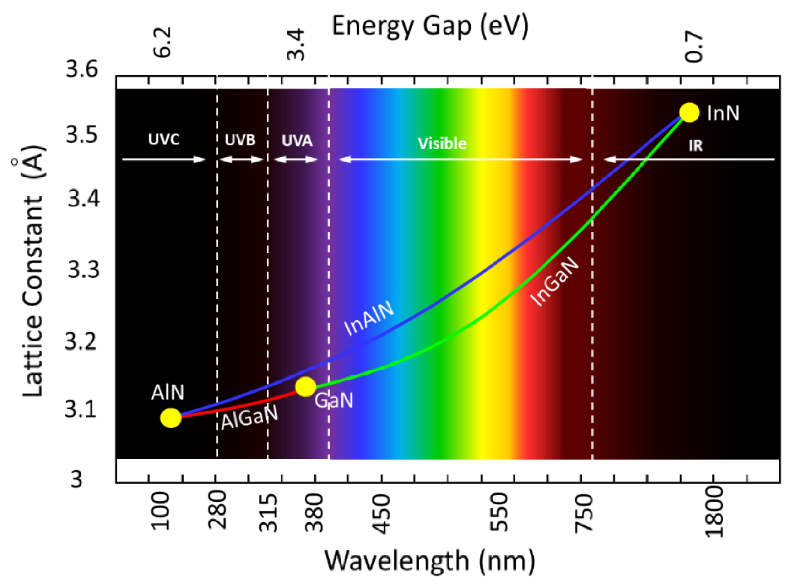
Figure 2.
(a) Schematic illustration of QCSE for single QW without (left) and with (right) internal electric field, F. EL denotes the luminescence energy, (b) calculated band profiles of InGaN/GaN MQW along c-axis of WZ structure.
Figure 2.
(a) Schematic illustration of QCSE for single QW without (left) and with (right) internal electric field, F. EL denotes the luminescence energy, (b) calculated band profiles of InGaN/GaN MQW along c-axis of WZ structure.
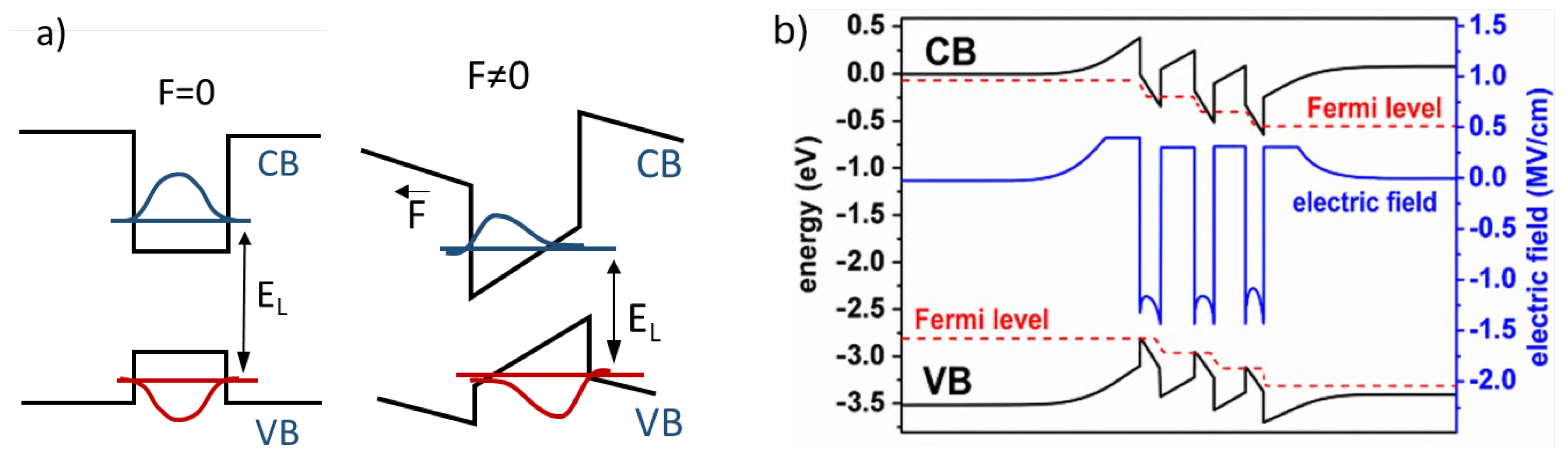
Figure 3.
Schematic of the (a) conventional InxGa1-xN/GaN QW, (b) two-layer staggered InxGa1-xN/InyGa1-yN QW and (c) three layer staggered InxGa1-xN/InyGa1-yN/InxGa1-xN QW structures.
Figure 3.
Schematic of the (a) conventional InxGa1-xN/GaN QW, (b) two-layer staggered InxGa1-xN/InyGa1-yN QW and (c) three layer staggered InxGa1-xN/InyGa1-yN/InxGa1-xN QW structures.
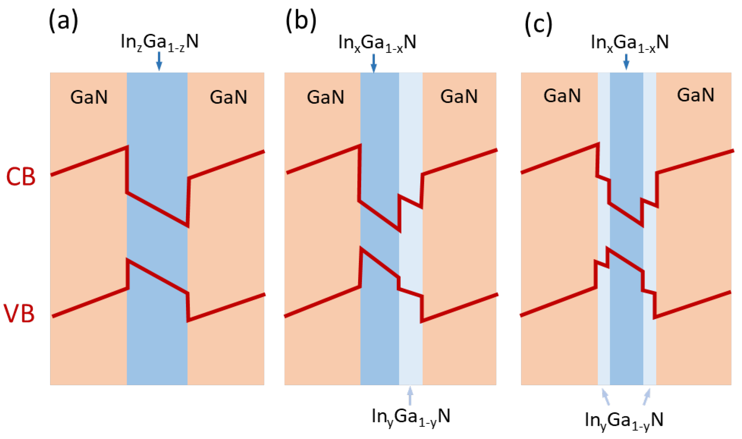
Figure 4.
Schematic of the valence band subbands in GaN and AlGaN.
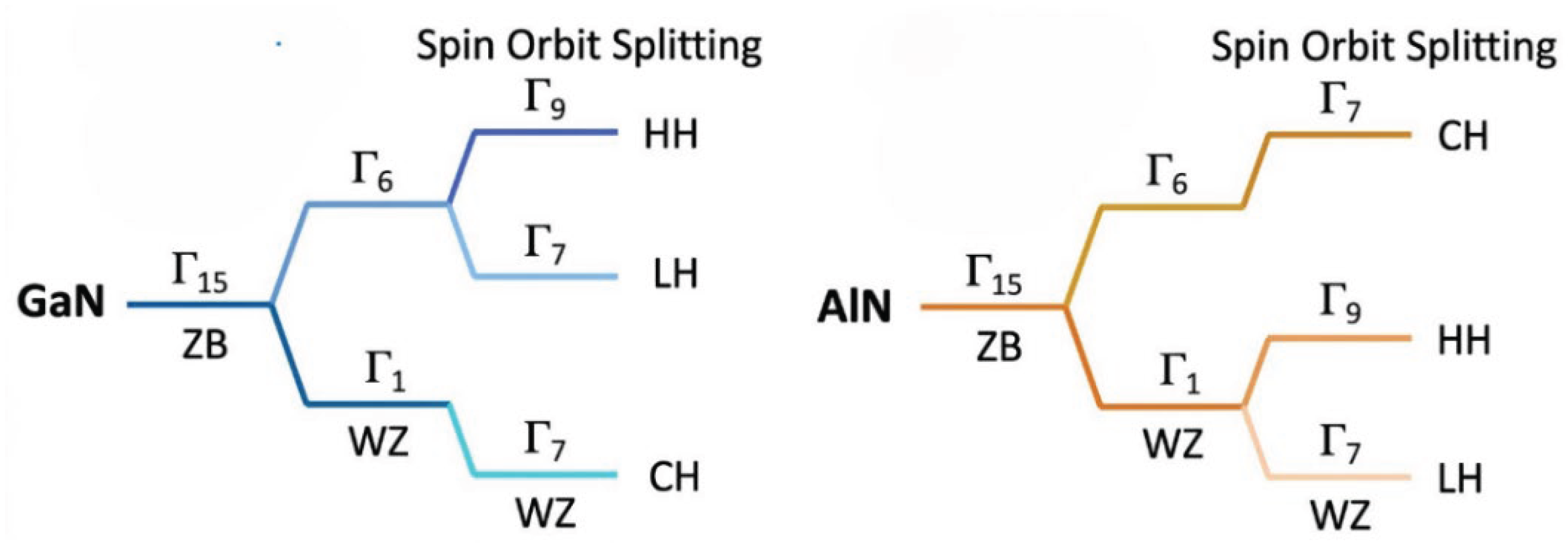
Figure 5.
Schematic diagram of a epitaxial layers of InGaN-based blue: (a) LEDs, (b) LDs.
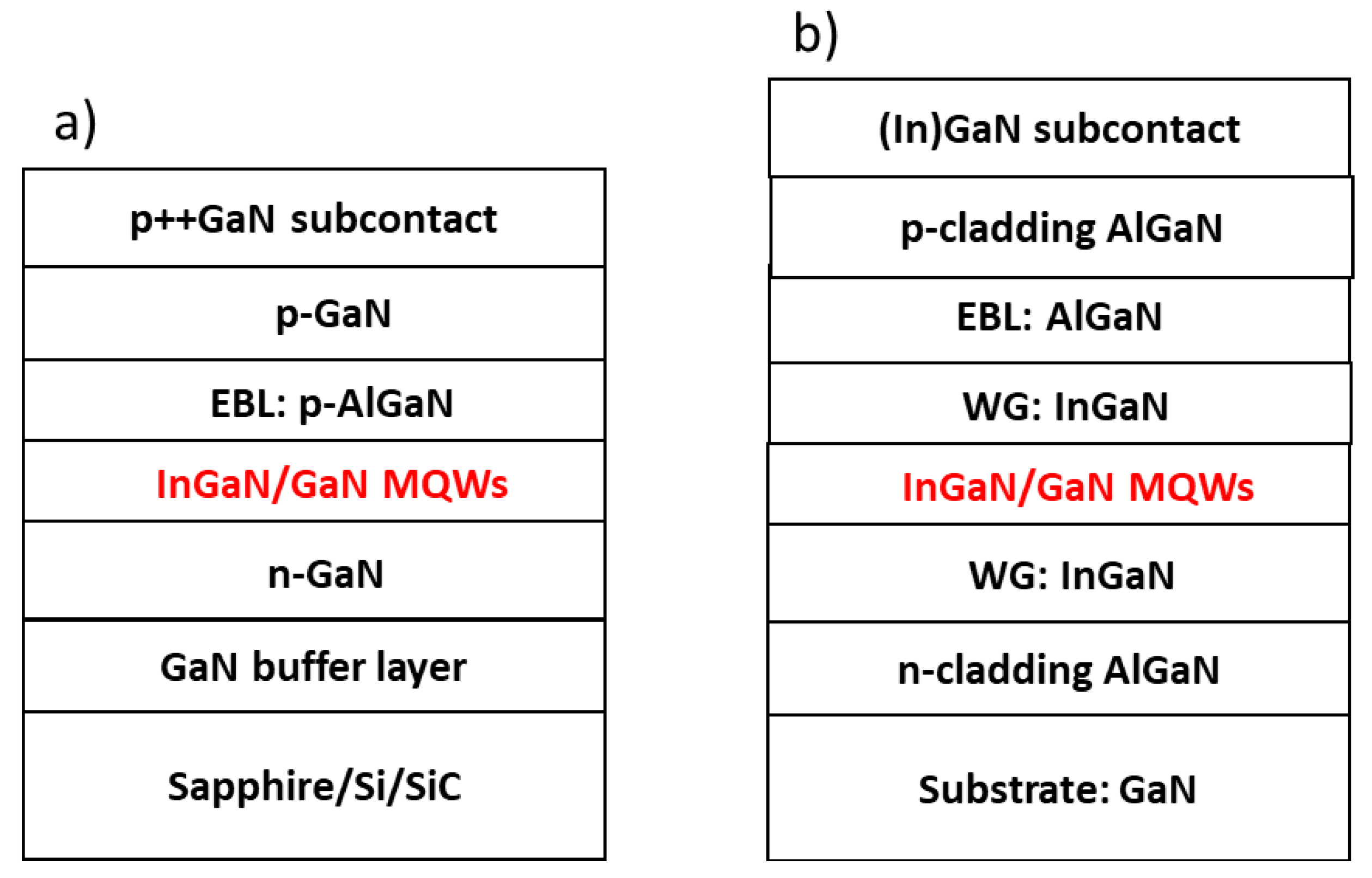
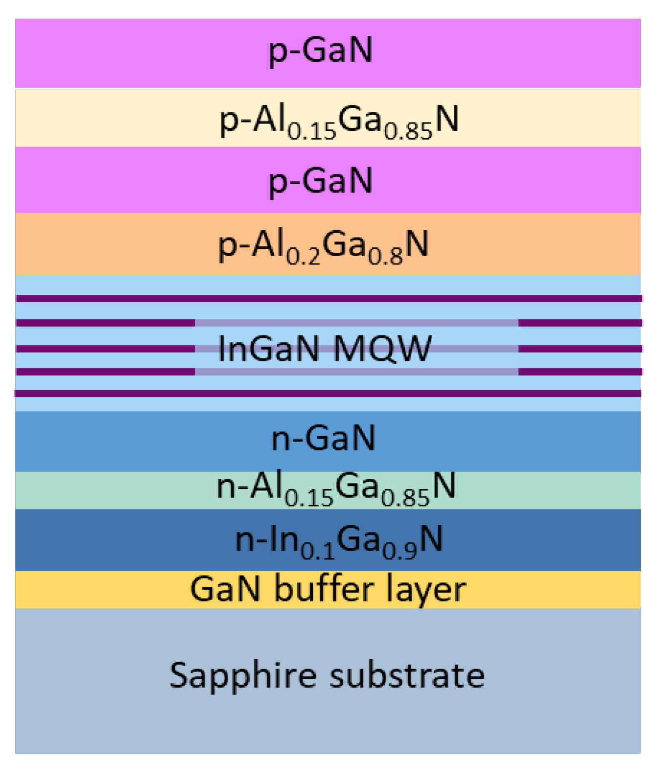
Figure 7.
The schematic of the UV LED epitaxial structure demonstrated by Li et al. [60] (based on their Figure 6).
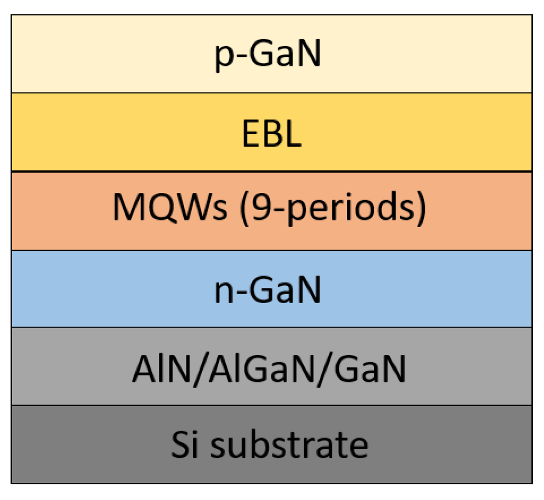
Figure 8.
The schematic of the UVA LD epitaxial structure fabricated by Taketomi et al. [65].
Figure 8.
The schematic of the UVA LD epitaxial structure fabricated by Taketomi et al. [65].
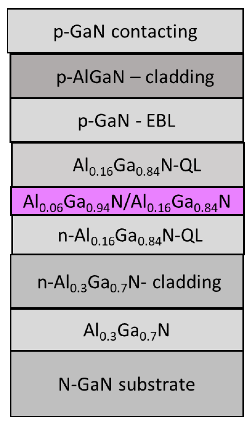
Figure 9.
EQE as a function of emission wavelength for UV, violet and blue emitters. Triangle refers to micro LED [79].
Figure 9.
EQE as a function of emission wavelength for UV, violet and blue emitters. Triangle refers to micro LED [79].
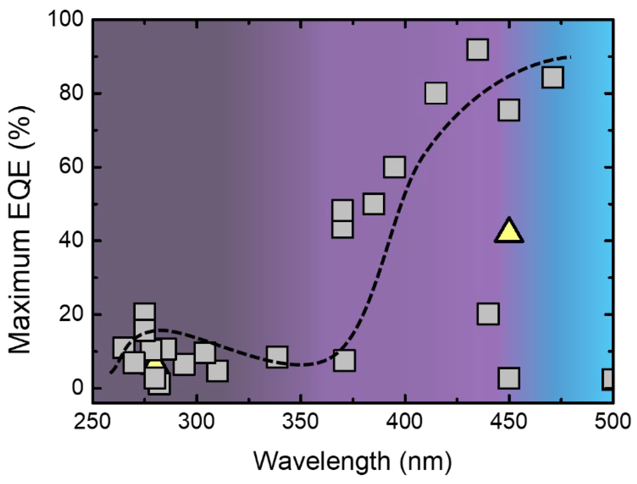
Figure 10.
Calculated band gaps, Eg, of mInN/nGaN and 1In0.33Ga0.67N/nGaN SLs as functions of effective In content, x=m/(m+n) in comparison with the experimental data (red dots). Based on Figure 1, Ref. [105] and on Figure 3, Ref. [107].
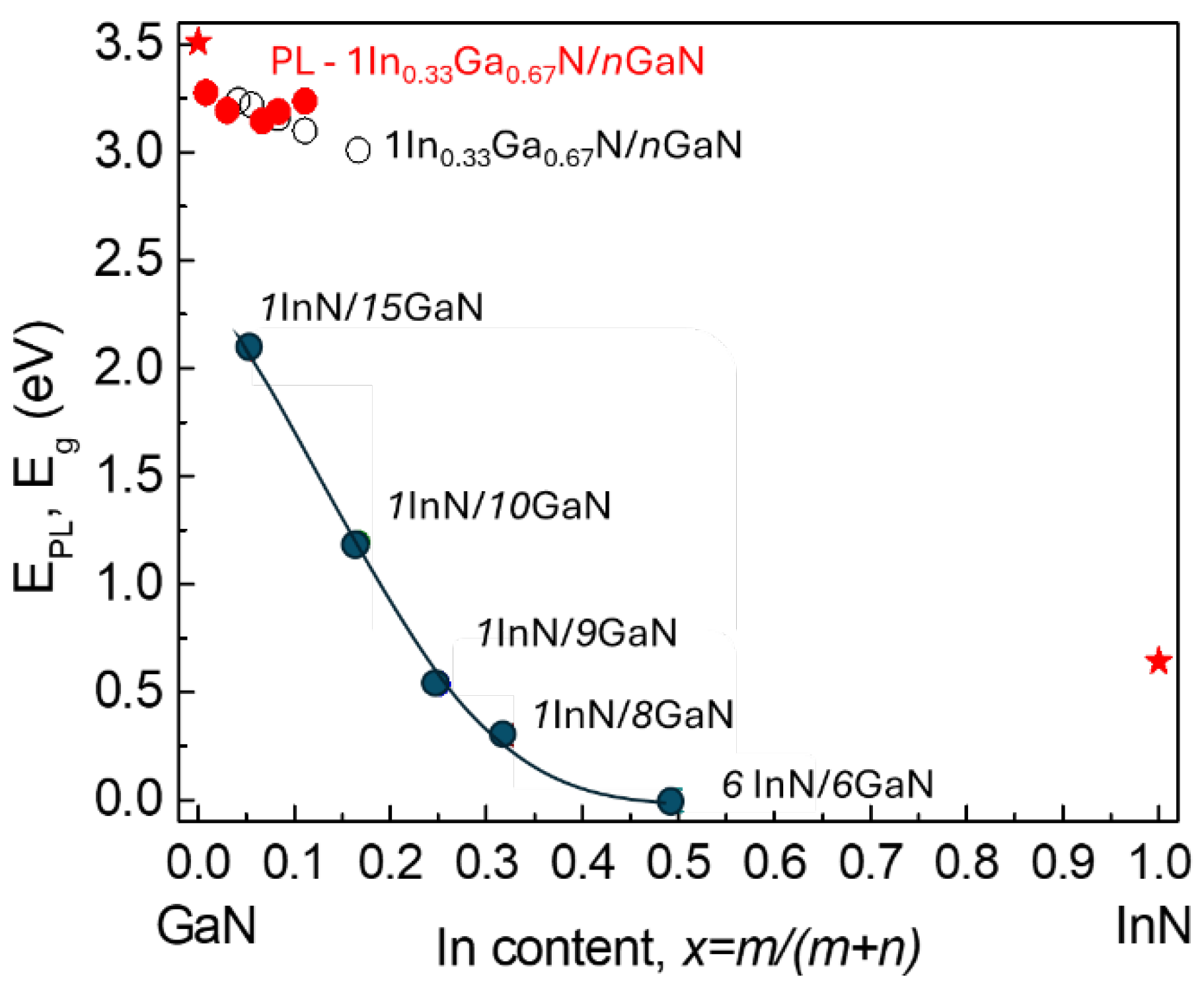
Figure 11.
Schematic diagram of the investigated in Ref. [112] SLs.
Figure 11.
Schematic diagram of the investigated in Ref. [112] SLs.
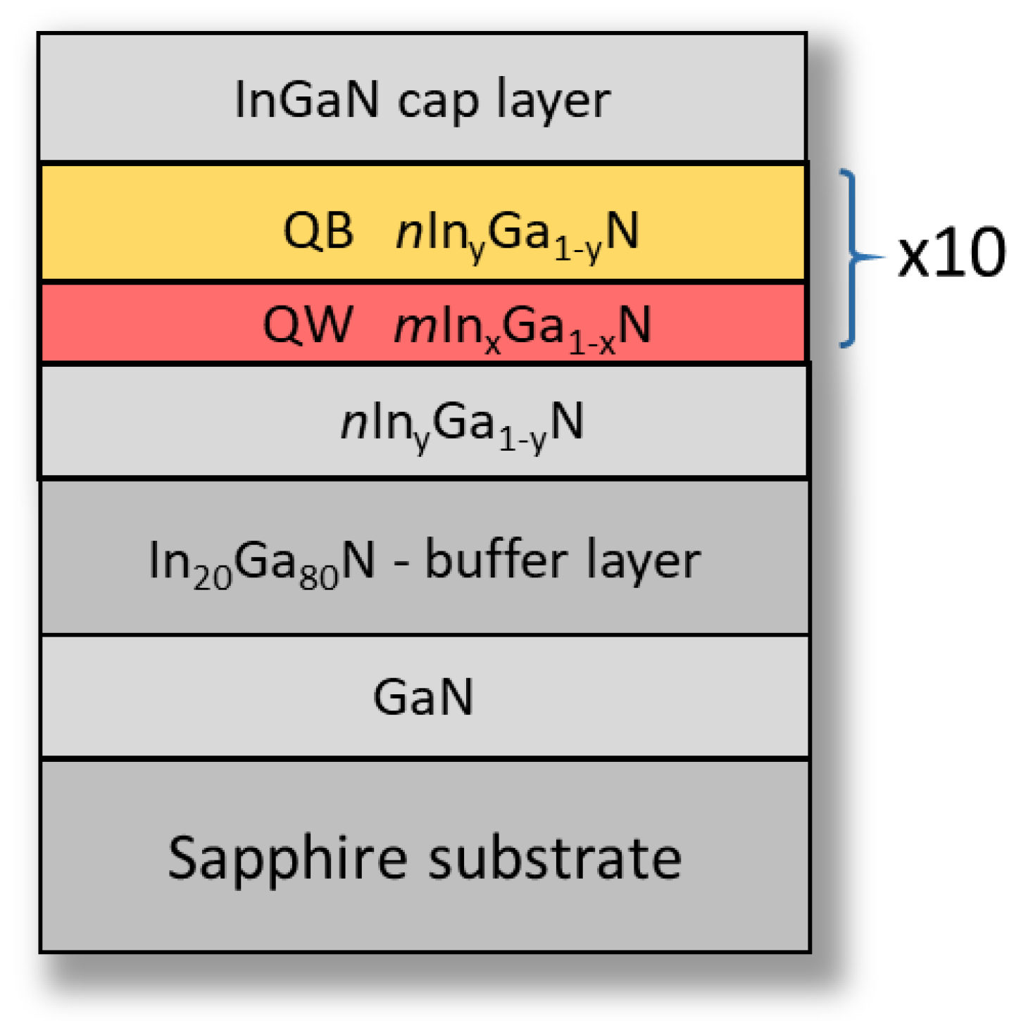
Figure 12.
Schematic of the epitaxial layer structure of the InGaN/GaN green LED described in the text. Based on Figure 1 of Ref. [116].
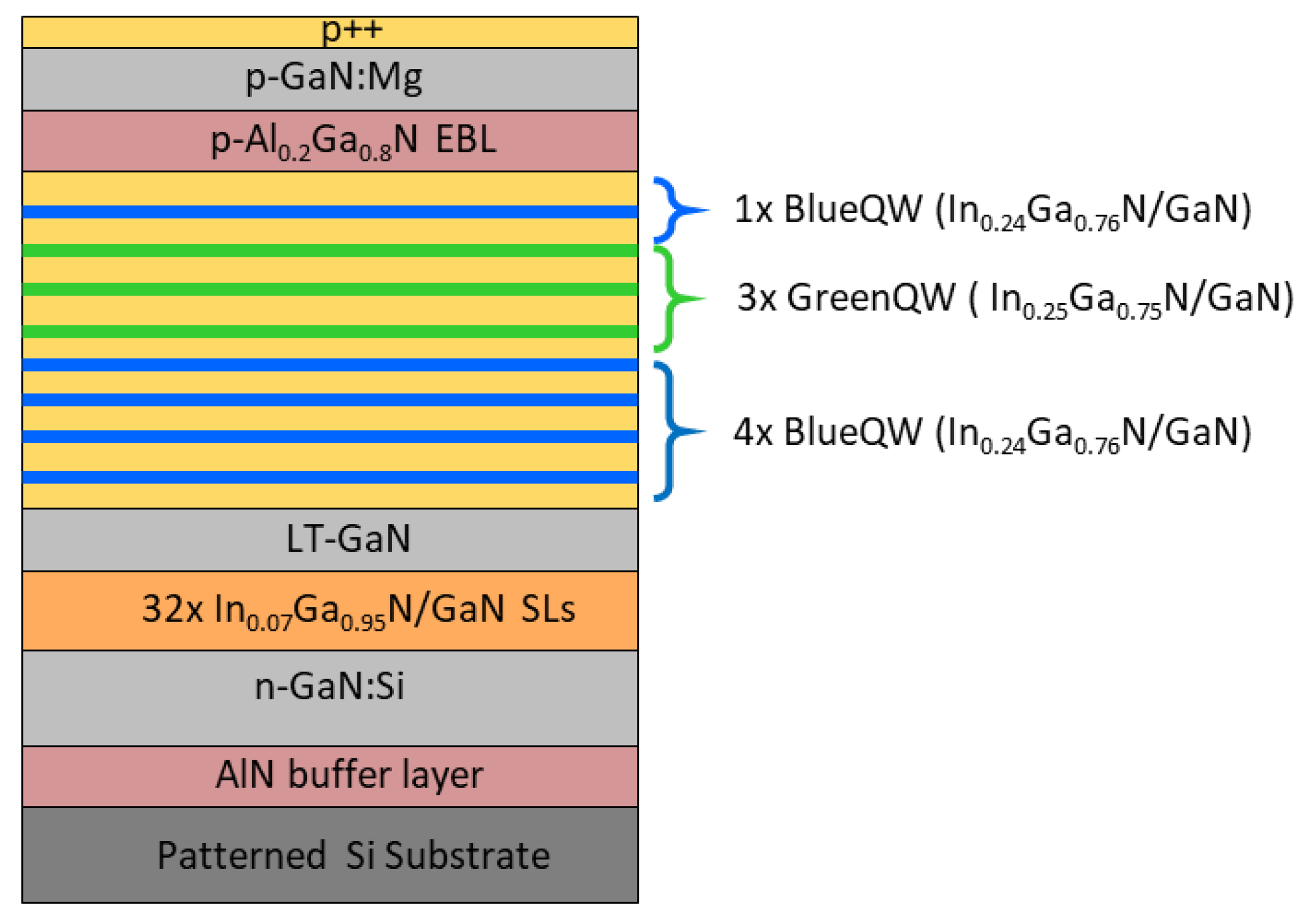
Figure 13.
The epitaxial layer structure of the cascaded blue and green μLEDs. Based on Figure 2, Ref. [49].
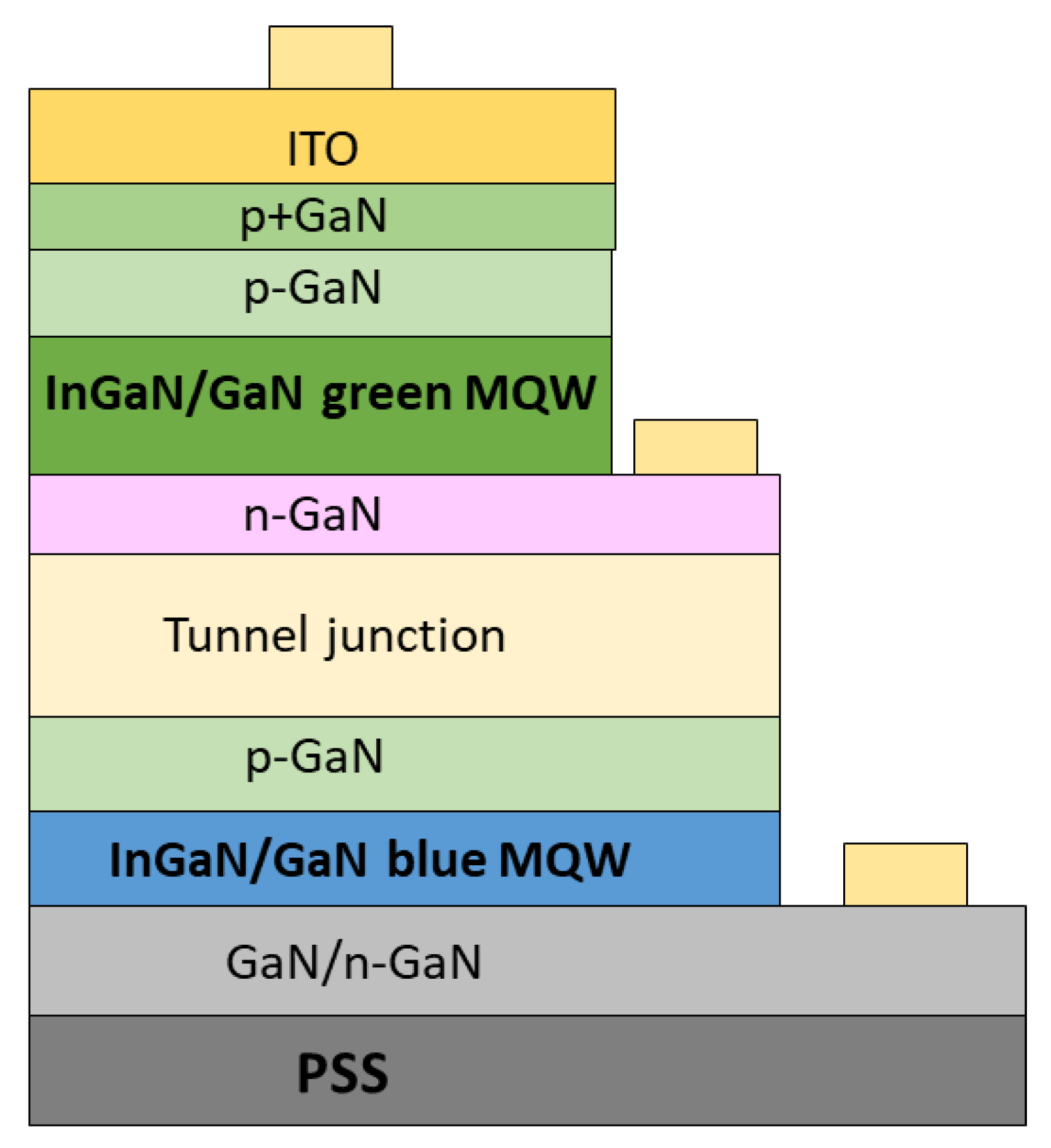
Figure 14.
Schematic of the N-polar InGaN/GaN nanowire excitonic LED heterostructure containing multiple quantum disks. Based on Figure 1 of Ref. [124].
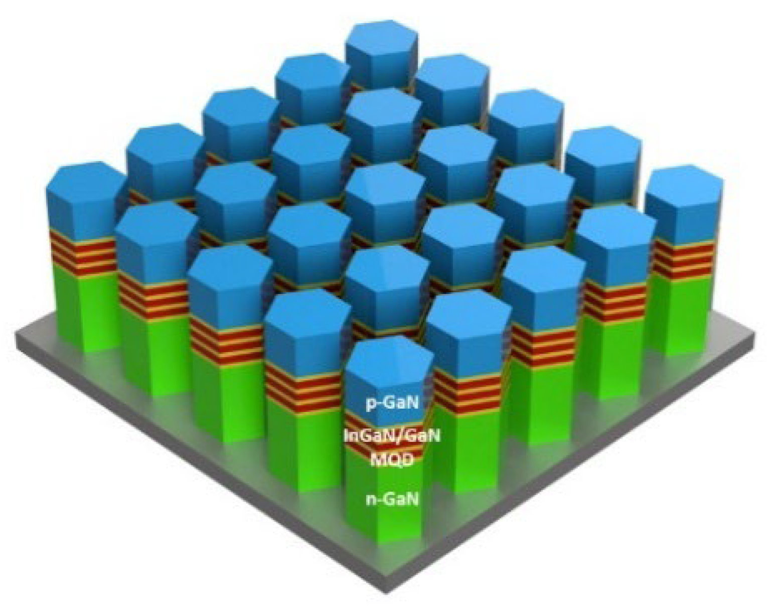
Figure 15.
EQE as a function of emission wavelength for all the emitters discussed in the text. Squares refers to conventional LEDs, triangle refers to micro LED.
Figure 15.
EQE as a function of emission wavelength for all the emitters discussed in the text. Squares refers to conventional LEDs, triangle refers to micro LED.
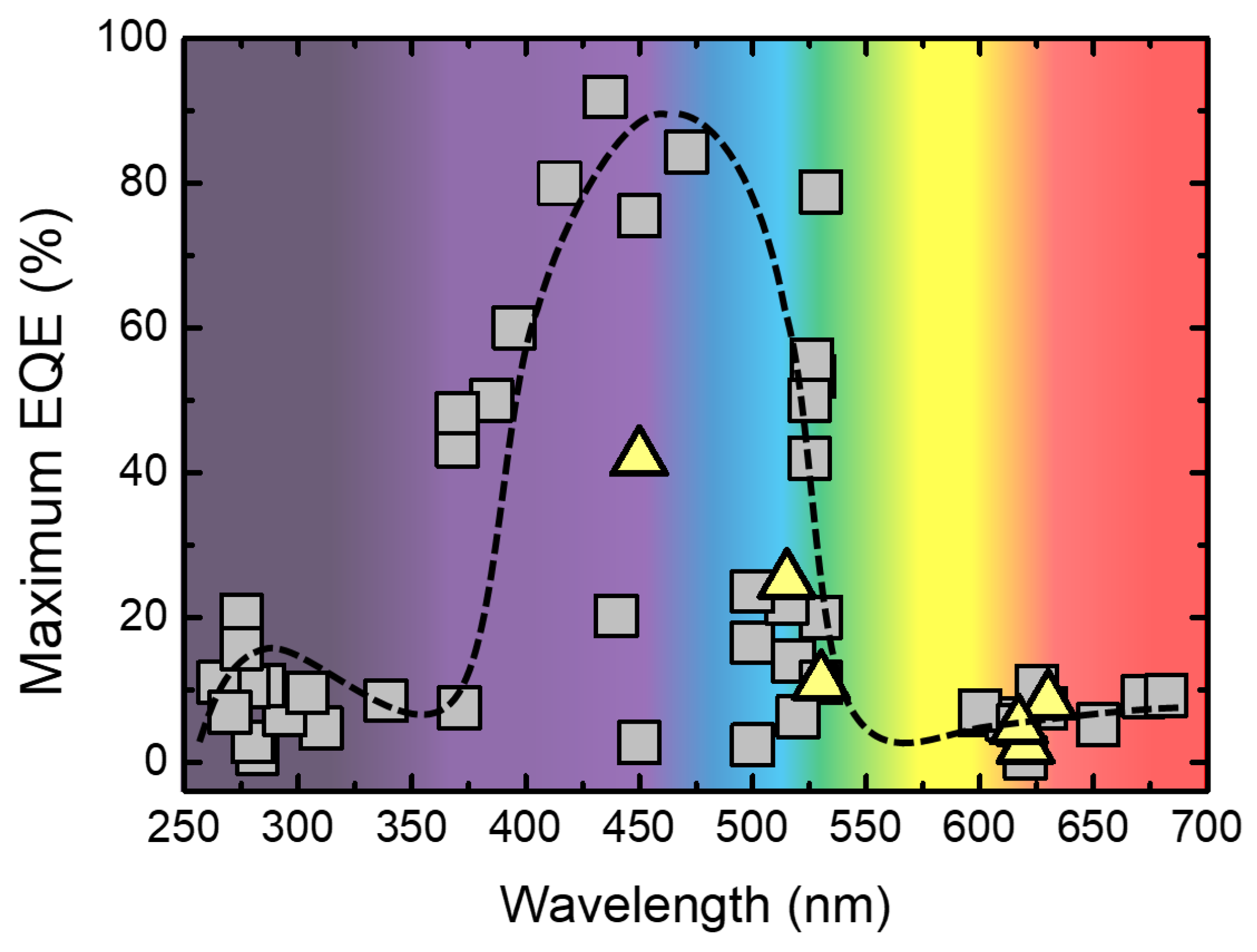
Figure 16.
The exemplary spectrum of white LED.
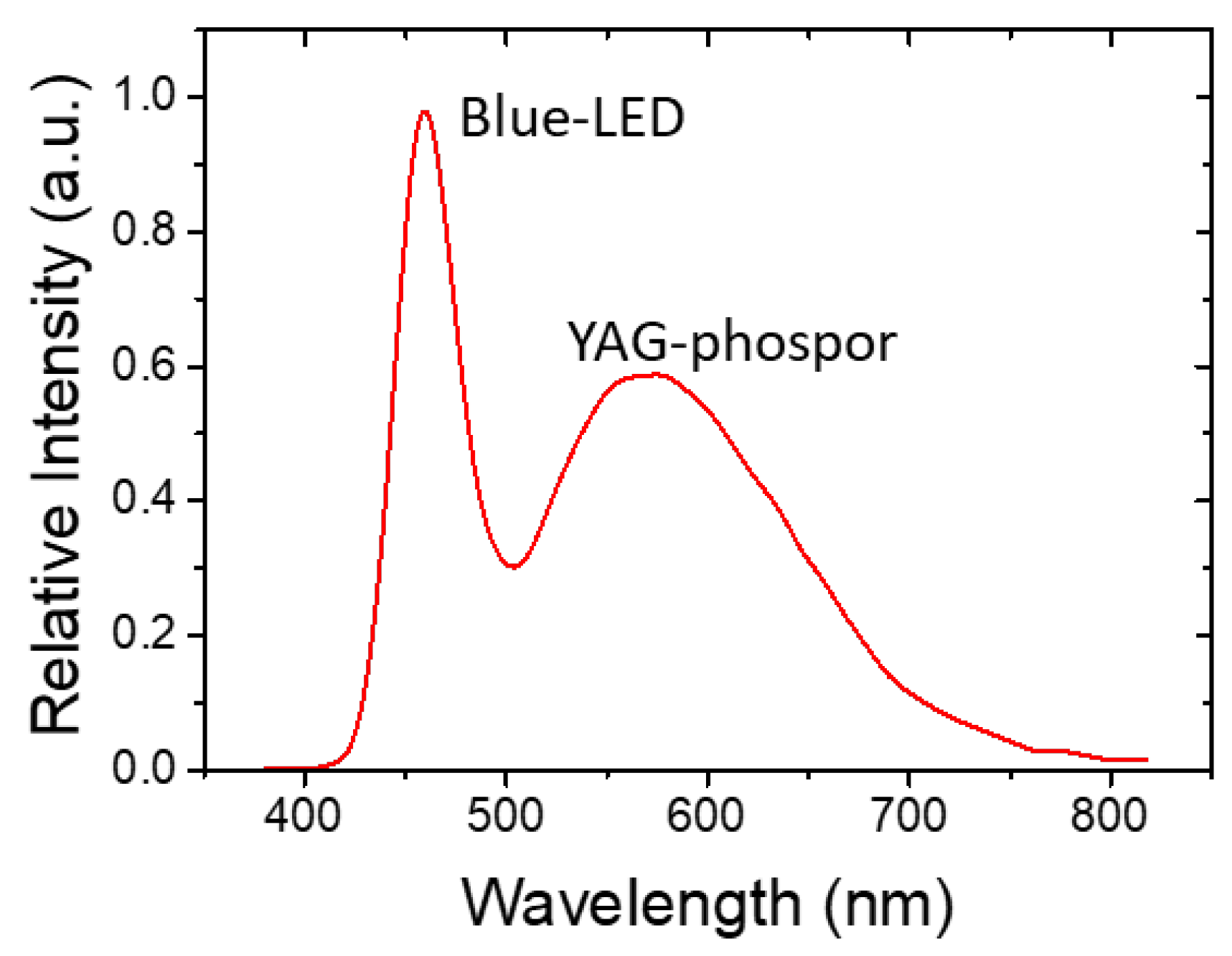
Figure 17.
Schematic of a) InGaN red, green, and blue MQW epitaxial structure, (b) the three-dimensional structure of the monolithic InGaN micro-LED. TJ denotes the tunnel junction. Based on Figure 2(a) and 3(c) of Ref. 145.
Figure 17.
Schematic of a) InGaN red, green, and blue MQW epitaxial structure, (b) the three-dimensional structure of the monolithic InGaN micro-LED. TJ denotes the tunnel junction. Based on Figure 2(a) and 3(c) of Ref. 145.
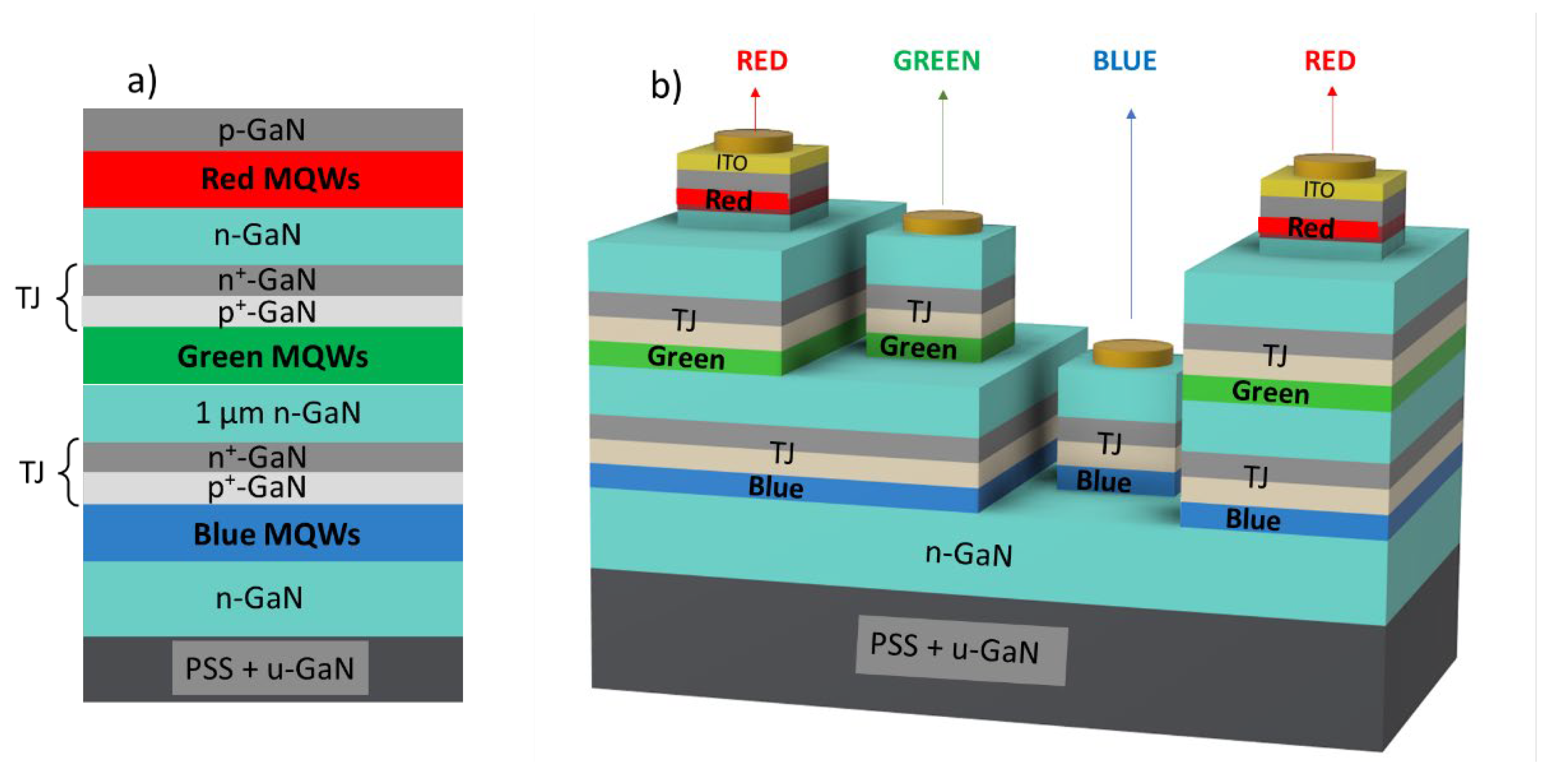

Table 1.
Comparison of different nitride blue, violet and UV light emitters.
| Characteristic | Wavelength | EQE | Year/Reference |
|---|---|---|---|
| Violet/blue | (nm) | (%) | |
| Zn-doped InGaN/GaN LEDs | 450 | 2.7 | 1994 Nakamura [43] |
| 2 nm thick InGaN/GaN SQW LEDs | 500 | 2.4 | 1994 Nakamura [44] |
| LEDs with optimized IQE and light extraction (ITO p-electrode and PSS) | 450 471 |
75.5 84.3 |
2006-2010 Narukawa [45,46,47] |
| LEDs with flip-chip architecture | 415 | 80 | 2015 Hurni [48] |
| cascaded micro-LEDs | 450 | 42 | 2021 Li [49] |
| nano-LEDs: sol-gel SiO₂ surface passivation | 440 | 20.2 | 2022 Sheen [50] |
| In0.15Ga0.85N/In0.02Ga0.98N LEDs | 435 | 91.9 | 2024 Choi [51] |
| In0.15Ga0.85N/In0.02Ga0.98N LDs * | 440 | 44.7 | 2024 Choi [51] |
| UVA | |||
| InGaN/AlGaN (In ~ 0) LEDs | 371 | 7.5 | 1998 Mukai [55] |
| LEDs with improved growth & technology | 385 | 49.8 | 2014 Muramoto [56] |
| Al0.06Ga0.94N/Al0.16Ga0.84N MQW LDs * | 338.6 | 8.5 | 2016 Taketomi [65] |
| Vertical LEDs with in situ AlN and ex situ AlGaN nucleation layer |
370 | 43.7 48.2 |
2018 Oh [57] |
| InGaN/GaN/AlGaN/GaN optimized LEDs | 395 | 60 | 2020 Li [60] |
| UVB | |||
| InAlGaN-based LEDs with high Al content | 282 | 1.2 | 2009 Hirayama [72] |
| LEDs with high-crystal-quality AlN templates | 280 | 2.78 | 2010 Fujioka [74] |
| LEDs with optimized carrier transport and AlGaN MQW design | 310 | 4.7 | 2020 Khan [75] |
| LEDs with increased Al content in AlGaN MQW | 294 | 6.5 | 2020 Khan [75] |
| Germicidal UV LED with heavily Si-doped n-AlGaN MQWs | 285 | 10.6 | 2023 Wang [77] |
| Ring-shaped micro-LEDs | 280 | 6.17 | 2024 Zhao [79] |
| LEDs with photonic crystal and nano-patterned substrates | 304 | 9.6 | 2025 Khan [76] |
| UVC—LEDs | |||
| Optimized chip encapsulation | 278 | 10.4 | 2012 Shatalov [84] |
| Improved growth, enhanced light extraction | 279 | 7.0 | 2014 Hirayama [85] |
| AlN template on PSS | 275 | 20.3 | 2017 Takano [87] |
| Optimized reflective p-electrodes | 279 | 9.0 | 2018 Maeda [88] |
| AlGaN/GaN/AlGaN tunnel junction | 265 | 11 | 2020 Pandey [89] |
| Nano-patterned light extraction | 273 | 5.19 | 2021 Zheng [90] |
| p-layer optical optimization | 275 | 15.7 | 2021Matsukura [91] |
| Optimized MQWs and tunneling junction | 270 | 6.9 | 2024 Liu [92] |
Table 2.
Comparison of different green-red LEDs.
| Characteristic | Wavelength | EQE | Year/Reference |
|---|---|---|---|
| Green | nm | % | |
| p-AlGaN/InGaN/n-GaN MQWs | 520 | 6.3 | 1995 Nakamura [113] |
| InGaN/GaN MQWs on c-plane patterned sapphire | 527 | 53.3 | 2018 Li [114] |
| Optimized V-pits in InGaN/GaN MQWs | 525 | 42 | 2018 Zhou [115] |
| Optimized InGaN/GaN MQWs on PSS | 526 | 55.6 | 2019 Lv [116] |
| AlGaN interlayers, Si substrate. | 525 | 50 | 2020 Guo [117] |
| In0.25Ga0.75N/In0.02Ga0.98N LEDs | 530 | 78.8 | 2024 Choi [51] |
| In0.25Ga0.75N/In0.02Ga0.98N LDs | 500 | 23.6 | 2024 Choi [51] |
| Cascaded μLEDs | 518 | 14 | 2021 Li [49] |
| Nanowire LEDs grown by PAMBE | 530 | 11.0 | 2022 Liu [123] |
| Submicron-scale μLEDs | 515 | 25.2 | 2023 Pandey [124] |
| 50 μm μLEDs | 500 | 16.5 | 2024 Smith [125] |
| Commercial LEDs | 520–540 | 15–35 | |
| Commercial LDs | 510–530 | 20–25 | |
| Yellow-amber | |||
| Hybrid MQW structures | 620 | 0.6 | 2016 Iida [131] |
| μLEDs based on QDs | 617 | 4.9 | 2022 Yu [132] |
| Stress relaxation + high carrier injection | 617 | 5.11 | 2022 Horng [133] |
| V-defect-engineered LEDs | 600 | 6.5 | Ewing [134] |
| QW engineering | 612 | 6.0 | 2023 Li [135] |
| 1μ μLEDs | 600 | 7.1 | 2024 Smith [125] |
| Red | |||
| Device-level engineering | 652 | 5.2 | 2022 Huang [137] |
| N-polar InGaN nanowires | 620 | 2.2 | 2022 Pandey [138] |
| Nanowire LEDs with optimized Mg doping | 630 | 8.3 | 2023 Pandey [139] |
| Grain coalescence in the composite buffer | 629 | 7.4 | 2023 Chen [140] |
| Planar InGaN LED-band engineering | 625 | 10.5 | 2023 Lee [141] |
| GaN on columnar structures on porous SiN | 672 | 9.1 | 2024 Xing [142] |
| GaN on columnar structures on porous SiN improved | 682 | 9.2 | 2025 Xing [143] |
Disclaimer/Publisher’s Note: The statements, opinions and data contained in all publications are solely those of the individual author(s) and contributor(s) and not of MDPI and/or the editor(s). MDPI and/or the editor(s) disclaim responsibility for any injury to people or property resulting from any ideas, methods, instructions or products referred to in the content. |
© 2026 by the authors. Licensee MDPI, Basel, Switzerland. This article is an open access article distributed under the terms and conditions of the Creative Commons Attribution (CC BY) license (http://creativecommons.org/licenses/by/4.0/).
Copyright: This open access article is published under a Creative Commons CC BY 4.0 license, which permit the free download, distribution, and reuse, provided that the author and preprint are cited in any reuse.


