

Submitted:
05 May 2026
Posted:
06 May 2026
You are already at the latest version
Abstract
This study investigates the effect of co-doping with nanographene on the properties of FTO layers produced by spray pyrolysis. The results show that co-doping with nanographene enhances phase separation processes within the bulk of the FTO layer. The inhomogeneities formed during phase separation are depleted of fluorine compared to the film bulk. Co-doping with nanographene also significantly modifies the optical properties of the FTO layers. Specifically, it alters the position and intensity of the peaks in the reflection spectra, indicating a change in the nature of the absorbing centers. Furthermore, the optical bandgap of the FTO layers decreases with an increasing degree of nanographene doping. Finally, co-doping with nanographene reduces the resistance of the FTO layers, which can be attributed to an increase in charge carrier mobility.
Keywords:
FTO (fluorine-doped tin oxide)
; graphene oxide
; spray pyrolysis
; transparent conducting oxides
; phase separation
; optical bandgap
; sheet resistance
; structural properties
; co-doping
; nanographene
1. Introduction
Currently, transparent conducting oxides are widely used in various fields of electronics, optoelectronics, and photovoltaics [1,2,3,4,5]. From a practical standpoint, indium tin oxide (ITO) appears to be the most promising, as it offers the best combination of high transparency and low resistivity among transparent conducting oxides [6,7]. However, its widespread use is constrained by the high cost of indium, since obtaining a material with the required combination of optical and electrophysical properties requires an indium oxide content of at least 90 wt% in ITO [8,9]. Among the materials considered as alternatives to ITO, fluorine-doped tin oxide (F-doped SnO₂ or FTO) attracts the greatest attention [10,11]. This material, having low cost and high technological availability, is almost comparable to ITO in terms of its optical properties. Furthermore, FTO films are thermally stable up to 300 °C and exhibit high resistance to aggressive chemical environments, which allows their use as substrates for the synthesis of active layers in various devices and structures of transparent electronics and photovoltaics [12,13]. At the same time, FTO films are inferior to ITO films in conductivity, which may adversely affect the performance of devices and structures based on them. In view of the foregoing, research efforts aimed at exploring ways to increase the electrical conductivity of FTO films are of significant scientific and practical interest.
FTO films obtained by physical and chemical deposition methods exhibit a micro- and nanocrystalline structure, and their conductivity is determined by the concentration of donor centers (interstitial Sn atoms, oxygen vacancies, and fluorine atoms in the oxygen sublattice) as well as by effects at the crystallite boundaries [14,15]; therefore, it depends on both the film composition and its structure. Recent studies have shown that introducing carbon nanostructures (fullerenes, nanotubes, and graphene) into the bulk of conducting oxides can significantly modify their structural and electrophysical properties [16,17,18,19]. However, the influence of carbon nanostructures on the characteristics of FTO layers remains poorly understood. This article presents the studies on the effect of co-doping with nanographene on the parameters of FTO layers produced via ultrasonic spray pyrolysis..
2. Experimental
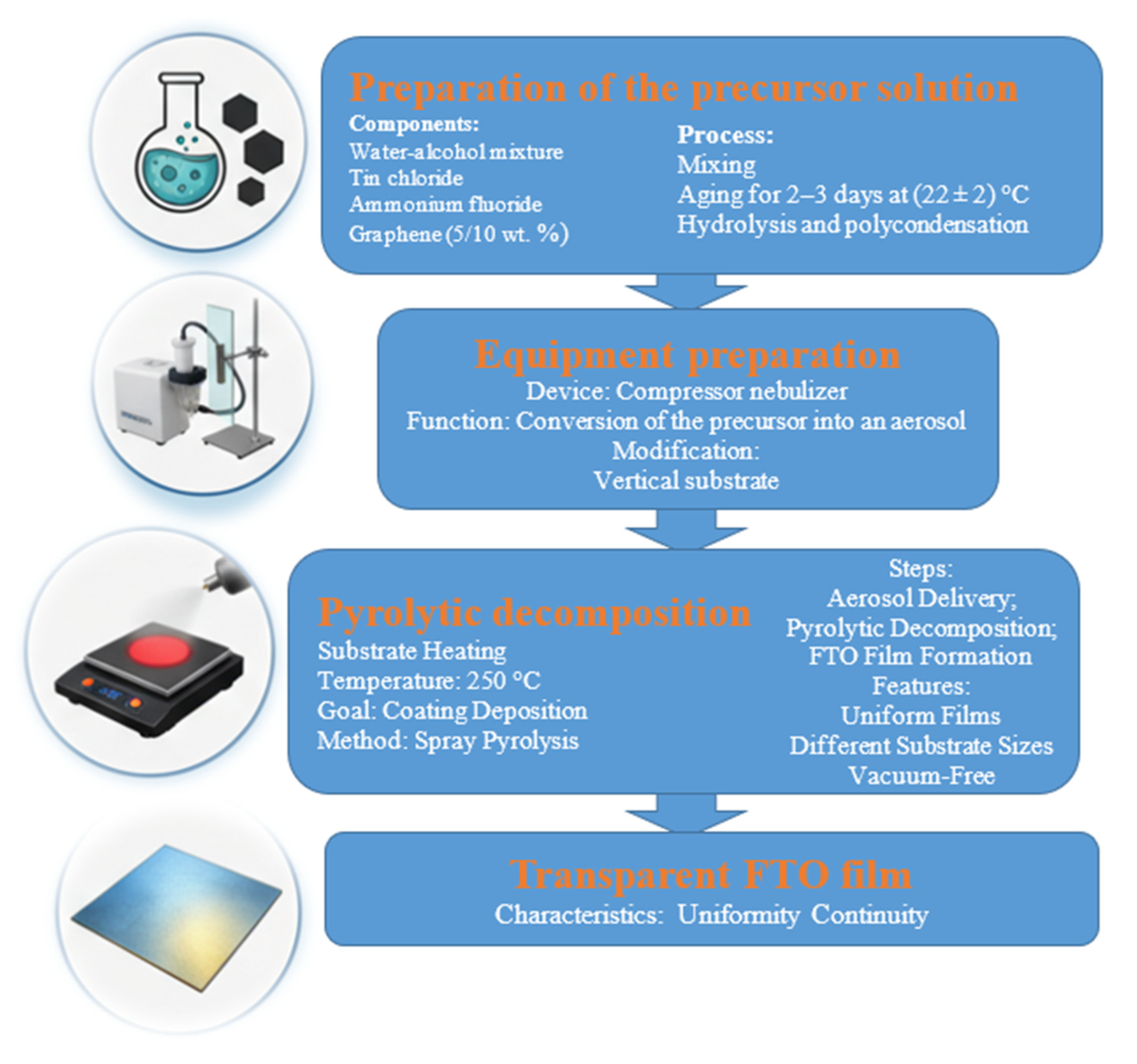
Transparent conducting films composed of fluorine-doped tin oxide (FTO), as well as those co-doped with nanographene (FTO:C), were prepared by spray pyrolysis using sol–gel technology. This approach enables the formation of uniform coatings on large-area substrates without the use of expensive vacuum equipment.
The examined layers were grown on a p-type silicon substrate with a resistivity of 4 Ω·cm. To form the FTO layers, a sol based on a water–alcohol mixture was prepared. Tin chloride and ammonium fluoride of at least ultrapure grade were selected as starting materials. An aqueous solution containing nanographene powder at a concentration of 2 mol% was introduced into the obtained sol. The concentration of the nanographene solution in the initial sol ranged from 6 to 12 mol%. The samples were labeled according to the content of the nanographene solution in the initial sol (FTO-0, the control sample containing no nanographene, and FTO-6 to FTO-12, samples containing from 6 to 12 mol% of the nanographene solution in the initial sol, respectively).
To break down agglomerates and ensure uniform particle distribution, the graphene-containing solutions were additionally subjected to ultrasonic treatment. Subsequently, all solutions were kept at room temperature (22 ± 2 °C) for 2–3 days to complete the hydrolysis processes and form a stable sol.
The films were deposited using a spray pyrolysis setup with pneumatic atomization. Cleaned Si substrates were fixed in the reaction chamber and heated to a temperature of 450–550 °C. A compressor jet nebulizer was employed to spray the solution, converting the sol into a finely dispersed aerosol under compressed air (pressure of about 2 atm). The aerosol stream was directed onto the heated substrate, resulting in the pyrolytic decomposition of the salts and the formation of the FTO film. Volatile reaction products and solvent residues were removed in the vapor phase. The vertical orientation of the substrate contributed to the uniformity of the resulting coatings. The spraying process persisted until the required film thickness was achieved, after which the samples were air-cooled.
The structural characteristics of the developed layers were studied using scanning electron microscopy and X-ray diffraction analysis, with a JEOL JSM-IT200 electron microscope and an Empyrean X-ray diffractometer from Malvern Panalytical. The band gap of the layers was determined by the Tauc method from adsorption spectra acquired with a YOKE M601S-x spectrophotometer. The sheet resistance (Rsheet) of the samples was measured by the four-probe method using a setup based on a Keithley 2805 source measure unit (SMU).
Figure 1.
Procedure for the fabrication of FTO films via spray pyrolysis.
3. Results and Discussion
Figure 2a–e present scanning electron microscopy images depicting the surface of FTO layers with different nanographene contents. Relief inhomogeneities are observed on the film surfaces, with both concentration and size exhibiting an increase corresponding to the rising content of nanographene in the analyzed layers. For instance, in FTO-12 layers the concentration of inhomogeneities per unit surface area is 2 to 2.5 times greater than that of layers without nanographene. Additionally, the average diameter of the inhomogeneities increases from 8–10 μm to 20–25 μm. This suggests that introducing nanographene into FTO films during synthesis stimulates phase separation processes.
Figure 2f shows an image of a cross-sectional cleavage passing through one of the phase inhomogeneities, obtained for the FTO-12 sample. The image reveals that the inhomogeneity extends throughout the entire thickness of the film, with its thickness surpassing the film thickness by a factor of 3 to 3.5.
To determine the composition of the phase inhomogeneities, studies of the elemental composition of the FTO films were conducted using energy-dispersive X-ray spectroscopy (EDS). Figure 3 illustrates the results of EDS mapping and the linear profile of the elemental composition obtained for the FTO-10 sample. The presented dependencies reveal that the observed inhomogeneities differ in composition from that of the film bulk. Specifically, in the region of the inhomogeneities, an increased intensity of tin and oxygen lines is observed, whereas the intensity of the fluorine line remains constant. Table 1 displays the elemental composition of the studied sample in mass and atomic fractions, averaged over the entire film surface shown in the image, as well as the composition determined at a point within a phase inhomogeneity.
The in-plane XRD pattern of the perovskite layer is shown in Figure 3. Strong diffraction peaks are observed at 14.2°, 28.5°, and 31.8°, which correlated to a crystal plane of (110), (220), and (310), respectively. The indexing of the peaks reveals that the CH3NH3PbI3-xClx perovskite layer has a tetragonal crystalline structure. The same structure is observed when perovskite is deposited on planar or nanotextured silicon substrates, coated with a TiO2 ETL [1,5]. Note also that a weak peak is observed at 12.6°, which corresponds to the crystal plane of (001). It shows that PbI2 was not fully converted into perovskite.
The results presented in Table 1 indicate that the inhomogeneities are enriched in tin and depleted in fluorine, which confirms the EDS mapping data. Meanwhile, the higher oxygen signal intensity obtained by EDS mapping does not indicate an increase in oxygen concentration within the phase formations, but is rather associated with an increase in the detection region thickness during EDS signal acquisition from the phase inhomogeneities. A slight increase in carbon concentration in the region of the phase inhomogeneity is also noted. However, a carbon background (12 to 14 at.%) is observed in the studied films, associated with traces of organic compounds used in the film synthesis. This makes it impossible to conclude whether the increase in EDS signal intensity is related to a higher content of nanographene particles in the region of the phase inhomogeneity.
Figure 4 presents the X-ray diffraction analysis data for graphene-containing FTO films. The spectra obtained indicate the presence of two crystalline phases of tin oxide in the studied films. Both phases belong to the space group P4₂/mnm, yet they exhibit different lattice parameters and unit cell volumes. These results may suggest that the crystalline structure of FTO in the bulk of the film and in the region of phase inhomogeneities has different parameters. Moreover, the differences in lattice parameters are attributed to the different fluorine content in the crystalline matrix of tin oxide – given that the ionic radius of fluorine exceeds that of oxygen, the lattice parameters of the phase inhomogeneities, which are depleted in fluorine, are smaller than those of the bulk layer with a higher content of F⁻ ions. These results also indicate that fluorine ions occupy positions in the oxygen sublattice during the synthesis of the studied films, rather than being localized at crystallite boundaries.
In the XRD patterns of the FTO-6 and FTO-12 samples, reflections associated with the (110) plane dominate, whereas in the spectra of the FTO-8 and FTO-10 samples, reflections associated with the (101) plane are dominant, indicating that these samples exhibit different preferred orientations of crystallization. Moreover, the samples with a preferred crystallization orientation (101) show higher crystalline quality, as evidenced by the higher intensity of the reflections in the XRD patterns and their smaller full width at half maximum.
Table 2 presents the dependence of the crystalline phase parameters of graphene-containing FTO layers. The variation of the lattice parameters with nanographene concentration is not monotonic. However, for samples with the same preferred crystallization plane, an increase in the difference between the unit cell volumes of different phases is observed with increasing nanographene content. This result confirms the electron microscopy data implying that an increase in graphene content within the FTO bulk promotes phase separation processes, leading to the development of a fluorine-depleted crystalline phase.
The process of fluorine-depleted phase formation during phase separation can be described in the following manner. Research indicates [16,19] that carbon nanostructures in polycrystalline FTO and SnO₂ films do not contribute to crystallite formation but are instead situated at the boundaries of these crystallites. When co-doping FTO films with graphene, certain fluorine ions, exhibiting higher electrical activity than oxygen ions, may adhere to graphene nanoparticles without engaging in the phase separation processes. However, it should be noted, that mechanisms underlying the intensification of phase separation processes in FTO layers co-doped with nanographene are not yet fully understood and necessitate additional investigation
Figure 5a shows the absorption spectra of the studied FTO films obtained at room temperature, and Figure 5b presents the same spectra plotted in Tauc coordinates.
The presented dependencies show that co-doping with nanographene significantly modifies the absorption spectra of the studied FTO layers. The FTO-0 sample contains no nanografen exhibits significant oscillations in absorptance. The observed positions of the maxima in the absorption spectrum are irregular, suggesting that these maxima are not associated with light reflection from the film–substrate interface, but instead arise from the wavelength dependence of the absorption coefficient. In the nanogaphene co-doped samples, these oscillations are substantially weaker, and the positions of the maxima differ from those in the FTO-0 sample. Furthermore, absorptance increases with increasing graphene content in the FTO layer and correlates with an increase in the concentration of phase inhomogeneities within its volume, suggesting that the increase in absorptance may be related to an increase in the content of phase inhomogeneities and the enhancement of the surface microrelief of the examined samples. The change in the positions of the absorptance oscillation maxima with increasing nanographene content is likely associated with a change in the nature of absorbing centers resulting from the phase separation processes.
The data presented in Figure 5b show that co-doping with nanographene leads to a decrease in the optical bandgap determined by the Tauc method. Specifically, the bandgap decreases from 4.4 eV in the graphene-free FTO-0 sample to 4.1 eV in the FTO-10 and FTO-12 samples, which have the highest nanographene content. Sheet resistance (Rₛₕₑₑₜ) measurements for the examined layers indicate that co-doping with nanographene produces a significant reduction (3–4 times) in Rₛₕₑₑₜ compared to undoped FTO layers (Table 3). This suggests that the observed change in the bandgap cannot be explained within the framework of the Burstein–Moss model but is apparently associated with a change in the lattice parameters of the FTO matrix during phase separation.
Notably, the Rₛₕₑₑₜ value depends non-monotonically on the nanographene content in the bulk of the FTO layer. The lowest Rₛₕₑₑₜ values are observed for the FTO-8 sample, while a further increase in graphene content leads to an increase in Rₛₕₑₑₜ.
Now consider the reasons that determine the effect of co-doping with nanographene on the sheet resistance of FTO layers. As it was shown above, during phase separation in FTO layers containing nanographene, fluorine-depleted phase inhomogeneities are generated, leading to a rise in fluorine content and, subsequently, in charge carrier concentration within the bulk of the main layer. However, EDS data reveal that the change in fluorine concentration due to phase separation processes is on the order of a few tenths of a percent, which is insufficient to explain the substantial reduction in sheet resistance observed. In our view, the decrease in sheet resistance in nanographene-co-doped samples is largely determined by an increase in charge carrier mobility. Indeed, studies [17,19] have reported an increase in charge carrier mobility in SnO₂ and FTO layers that are co-doped with graphene. Reference [19] attributes this increase in mobility to a lowering of potential barriers and a decrease in the concentration of scattering centers at crystallite interfaces due to the localization of nanographene particles at these interfaces. The rise in sheet resistance in the FTO-10 and FTO-12 samples correlates with an increase in size and number of phase inhomogeneities in the volume of FTO layers and could be related with increasing the intensity of charge carrier scattering on the interfaces of these inhomogeneities.
4. Conclusions
Thus, the present study demonstrates that co-doping with nanographene leads to significant changes in the structural, optical, and electrophysical properties of FTO layers obtained by spray pyrolysis. The incorporation of graphene induces the formation of fluorine-depleted phase inhomogeneities within the FTO bulk, and an increase in nanographene content intensifies the phase separation processes. The analysis of the absorption spectra reveals that both the absorption intensity and the nature of the absorbing centers depend on the graphene content in the FTO layers. The optical bandgap of the FTO layers decreases with increasing graphene content. This decrease is not associated with the Burstein–Moss effect; instead, it arises from changes in the lattice parameters of the FTO layer caused by phase separation. The incorporation of graphene into FTO leads to a decrease in sheet resistance, which is attributed to an increase in charge carrier mobility. The relationship between sheet resistance and graphene concentration exhibits a non-monotonic behavior, which is due to increased charge carrier scattering at the interfaces of phase inhomogeneities, the concentration of which rises with the level of co-doping. Thus, our results indicate that co-doping with graphene can be used for the controlled modification of the optical and electrophysical parameters of FTO layers.
The work was carried out with the support of the joint Uzbek–Belarusian project “Mechanisms of Formation and Photoelectric Properties of Complex Oxide Films with Tunable Bandgap for the Fabrication of Photosensitive Structures in the Short-Wavelength Range”, registration number in the Republic of Uzbekistan FL-8824063322, registration number in the Republic of Belarus BRFFI-T25UZB-111.
References
- Datt, R.; Alsayyed, H.; Dhall, S.; et al. Top electrode materials for semi-transparent perovskite solar cells: A review. Discov. Appl. Sci. 2025, 7, 1348. [Google Scholar] [CrossRef] [PubMed]
- He, Y.; Wang, X.; Gao, Y.; Hou, Y.; Wan, Q. Oxide-based thin film transistors for flexible electronics. J. Semicond. 2018, 39, 011005. [Google Scholar] [CrossRef]
- Untila, G.G.; Kost, T.N.; Chebotareva, A.B.; Timofeyev, M.A. Optimization of the deposition and annealing conditions of fluorine-doped indium oxide films for silicon solar cells. Semiconductors 2013, 47, 415–421. [Google Scholar] [CrossRef]
- Wager, J.F. Transparent Electronics. Science 2003, 300, 1245. [Google Scholar] [CrossRef] [PubMed]
- Kang, D.Y.; Kim, B.H.; Lee, T.H.; Shim, J.W.; Kim, S.; Sung, H.J.; Chang, K.J.; Kim, T.G. Dopant Tunable Ultrathin Transparent Conductive Oxides for Efficient Energy Conversion Devices. Nano-Micro Lett. 2021, 13, 211. [Google Scholar] [CrossRef] [PubMed]
- Aksenova, V.V.; Smirnova, I.P.; Markov, L.K.; Pavlyuchenko, A.S.; Yagovkina, M.A. Effect of oxygen on the formation process of nanostructured indium tin oxide films. Phys. Solid State 2023, 65, 2079. [Google Scholar]
- Khan, M.Z.H. Pretreatment of ITO Electrode and Its Physiochemical Properties: Towards Device Fabrication. Surf. Eng. Appl. Electrochem. 2016, 52, 547–564. [Google Scholar] [CrossRef]
- Kudryashov, D.A.; Maksimova, A.A.; Vyacheslavova, E.A.; Uvarov, A.V.; Morozov, I.A.; Baranov, A.I.; Monastyrenko, A.O.; Gudovskikh, A.S. Study of the influence of the design features of a magnetron sputtering system on the electrical and optical properties of indium tin oxide films. Semiconductors 2021, 55, 360. [Google Scholar]
- Deng, W.; et al. Characteristics of Indium Tin Oxide Films Deposited by DC and RF Magnetron Sputtering. Jpn. J. Appl. Phys. 2001, 40, 3364. [Google Scholar] [CrossRef]
- Saehana, S.; Iswomiharjo, D.; Aprilia, A. Investigation of experimental parameters in fabrication of Fluorine-doped Tin Oxide (FTO) using spray pyrolysis. Int. J. Heat Technol. 2025, 43, 1076–1084. [Google Scholar] [CrossRef]
- Kumar, K.D.A.; Valanarasu, S.; Jeyadheepan, K.; et al. Evaluation of the physical, optical, and electrical properties of SnO₂:F thin films prepared by nebulized spray pyrolysis for optoelectronics. J. Mater. Sci. Mater. Electron. 2018, 29, 3648–3656. [Google Scholar] [CrossRef]
- Kafle, M.; et al. Effect of calcination environments and plasma treatment on structural, optical and electrical properties of FTO transparent thin films. AIP Adv. 2017, 7, 075101. [Google Scholar] [CrossRef]
- Plá Cid, C.C.; Spada, E.R.; Sartorelli, M.L. Effect of the cathodic polarization on structural and morphological proprieties of FTO and ITO thin films. Appl. Surf. Sci. 2013, 273, 603–606. [Google Scholar] [CrossRef]
- Ramaiah, K.S.; Raja, V.S. Structural and electrical properties of fluorine doped tin oxide films prepared by spray-pyrolysis technique. Appl. Surf. Sci. 2006, 253, 1451–1458. [Google Scholar] [CrossRef]
- Agashe, C.; Hüpkes, J.; Schöpe, G.; Berginski, M. Physical properties of highly oriented spray-deposited fluorine-doped tin dioxide films as transparent conductor. Sol. Energy Mater. Sol. Cells 2009, 93, 1256–1262. [Google Scholar] [CrossRef]
- Abdulzahraa, H.G.; Mohammed, M.K.A.; Raoof, A.S.M. Tin oxide/reduced graphene oxide hybrid as a hole blocking layer for improving 2D/3D heterostructured perovskite-based photovoltaics. Surf. Interfaces 2022, 31, 102092. [Google Scholar] [CrossRef]
- Das, P.; Pal, B.; Datta, J.; Das, M.; Sil, S.; Ray, P.P. Improved charge transport properties of graphene incorporated tin oxide based Schottky diode over pure one. J. Phys. Chem. Solids 2021, 148, 109706. [Google Scholar] [CrossRef]
- Go, L.; Macaraig, L.; Enriques, E. Few-layer-graphene as intercalating agent for spray-pyrolysed fluorine-doped tin oxide transparent conducting electrode. Bull. Mater. Sci. 2020, 43, 65. [Google Scholar] [CrossRef]
- Wenhao, C.; Wang, L.; Wang, L.; Wang, G.; Yu, J.; Zhao, H. Preparation of Fluorine-doped Tin Oxide-Graphene Composite Films and Study of Its Structure and Properties. J. Chin. Ceram. Soc. 2019, 47, 1484. [Google Scholar]
Figure 2.
Scanning electron microscopy images of the surface of FTO layers co-doped with graphene: (a) FTO-0; (b) FTO-6; (c) FTO-8; (d) FTO-10; (e) FTO-12; (f) cross-sectional cleavage image passing through a phase inhomogeneity of the FTO-12 sample.
Figure 2.
Scanning electron microscopy images of the surface of FTO layers co-doped with graphene: (a) FTO-0; (b) FTO-6; (c) FTO-8; (d) FTO-10; (e) FTO-12; (f) cross-sectional cleavage image passing through a phase inhomogeneity of the FTO-12 sample.
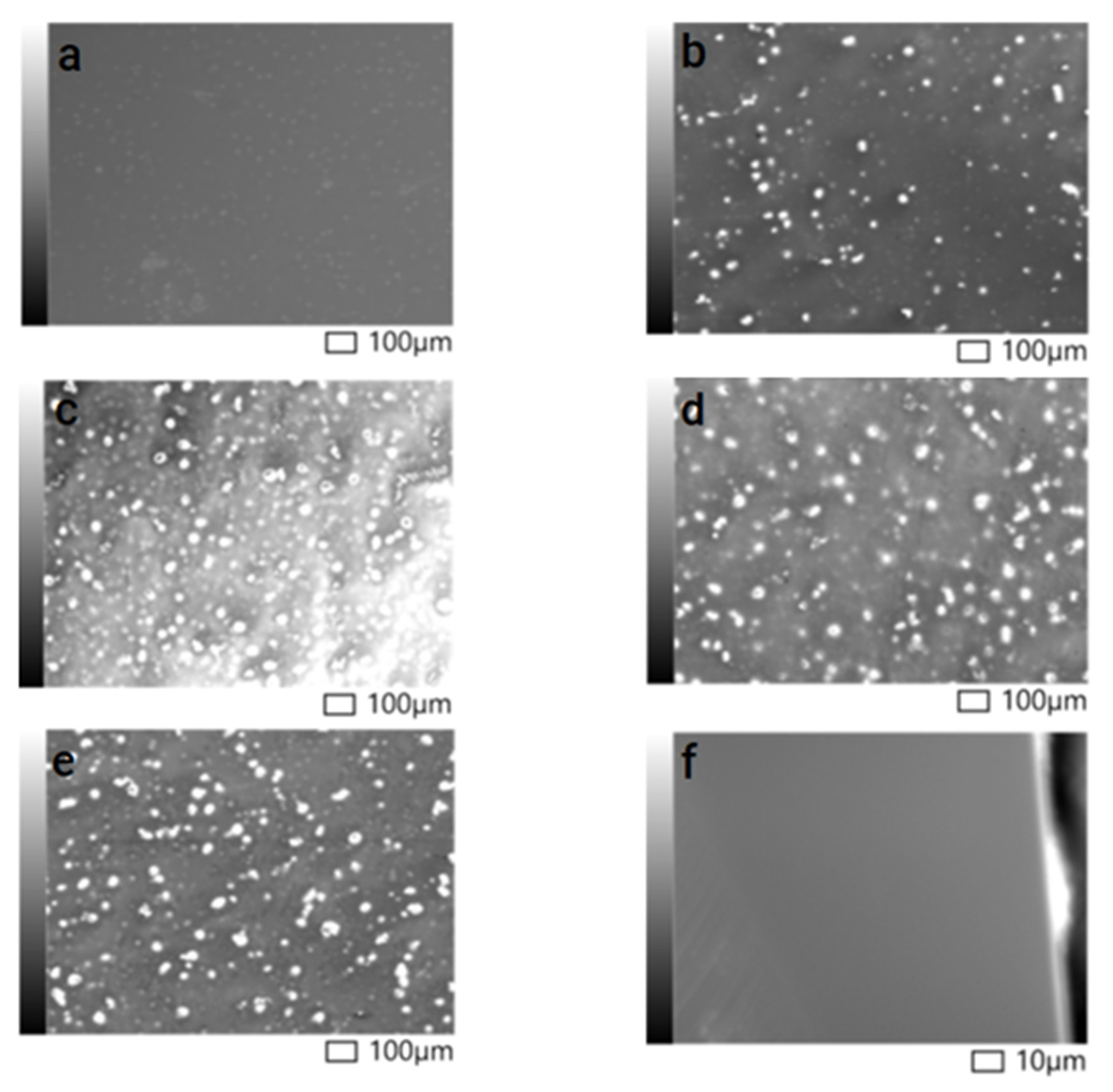
Figure 3.
Image of a phase inhomogeneity (a) and EDS mapping results in the region of the phase inhomogeneity (b–e) obtained for the FTO-10 film; (f, j) EDS mapping of the FTO-10 film along the line shown in Figure 2f.
Figure 3.
Image of a phase inhomogeneity (a) and EDS mapping results in the region of the phase inhomogeneity (b–e) obtained for the FTO-10 film; (f, j) EDS mapping of the FTO-10 film along the line shown in Figure 2f.
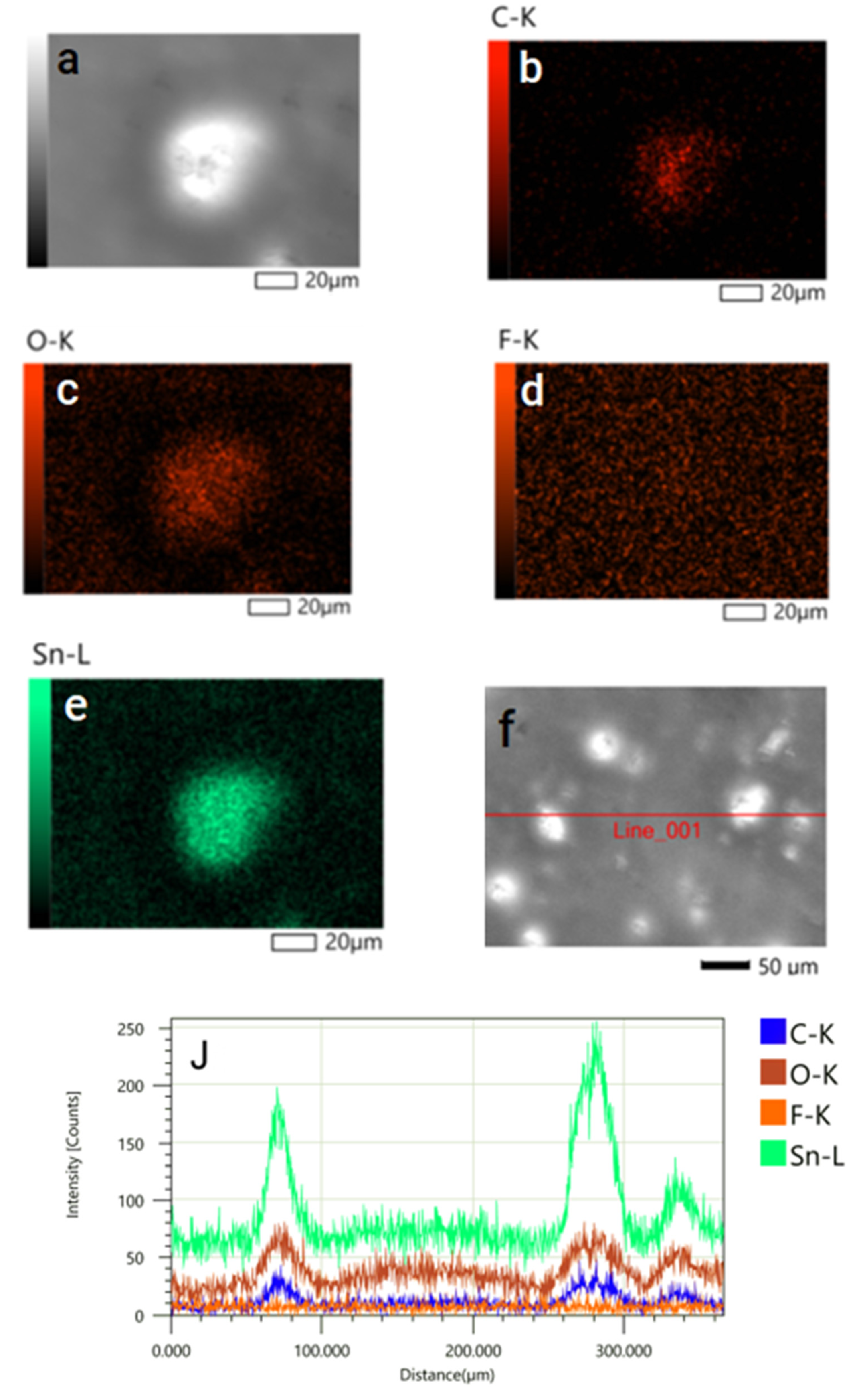
Figure 4.
XRD analysis data for FTO films containing nanographene: (1) FTO-6, (2) FTO-8, (3) FTO-10, (4) FTO-12. The arrows indicate the positions of peaks corresponding to different phases for the FTO-10 and FTO-12 samples.
Figure 4.
XRD analysis data for FTO films containing nanographene: (1) FTO-6, (2) FTO-8, (3) FTO-10, (4) FTO-12. The arrows indicate the positions of peaks corresponding to different phases for the FTO-10 and FTO-12 samples.
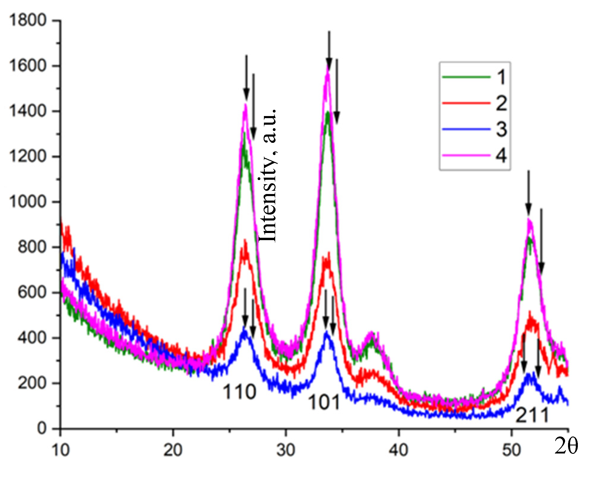
Figure 5.
Absorption spectra of the studied FTO layers (a); reflection spectra of the FTO layers plotted in Tauc coordinates (b).
Figure 5.
Absorption spectra of the studied FTO layers (a); reflection spectra of the FTO layers plotted in Tauc coordinates (b).
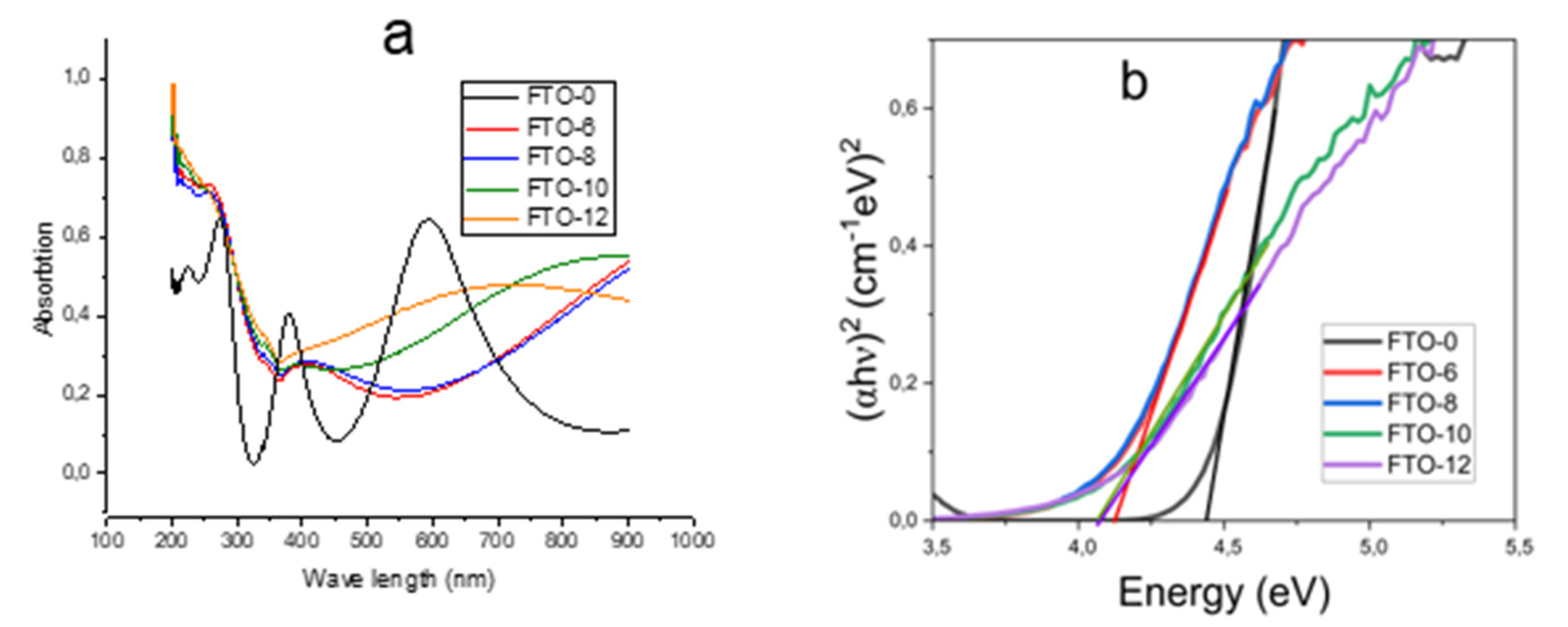

Table 1.
Elemental composition of the FTO-10 film according to EDS mapping.
| Element | Surface-averaged value | Value at the phase inhomogeneity point | ||
|---|---|---|---|---|
| mass % | atomic % | mass % | atomic % | |
| С | 6.23±0.0 2 | 12.36±0.05 | 6.23±0.02 | 12.88±0.04 |
| О | 52.21±0.18 | 77.78±0.27 | 49.39±0.16 | 76.70±0.25 |
| F | 1.44±0.09 | 1.80±0.11 | 1.03±0.07 | 1.35±0.09 |
| Sn | 40.12±0.12 | 8.06±0.02 | 43.35±0.11 | 9.07±0.02 |
Table 2.
Elemental composition of the FTO-10 film according to EDS mapping.
| FTO-6 | FTO-8 | FTO-10 | FTO-12 | |
|---|---|---|---|---|
| Preferred crystallographic plane | 101 | 110 | 110 | 101 |
| a1 | 4.7900 | 4.7552 | 4.7840 | 4.7552 |
| a2 | 4.7150 | 4.7380 | 4.6855 | 4.6537 |
| с1 | 3.1990 | 3.1992 | 3.2160 | 3.1992 |
| с2 | 3.1940 | 3.1180 | 3.1679 | 3.1577 |
| V1/V2 | 73.40/71.01 | 72.34/69.99 | 73.60/69.55 | 72.34/68.39 |
Table 3.
Sheet resistance values of FTO samples co-doped with graphene.
| FTO-0 | FTO-6 | FTO-8 | FTO-10 | FTO-12 | |
|---|---|---|---|---|---|
| Rsheet (Ω/□) | 64030 | 14850 | 12450 | 13500 | 18540 |
Disclaimer/Publisher’s Note: The statements, opinions and data contained in all publications are solely those of the individual author(s) and contributor(s) and not of MDPI and/or the editor(s). MDPI and/or the editor(s) disclaim responsibility for any injury to people or property resulting from any ideas, methods, instructions or products referred to in the content. |
© 2026 by the authors. Licensee MDPI, Basel, Switzerland. This article is an open access article distributed under the terms and conditions of the Creative Commons Attribution (CC BY) license (http://creativecommons.org/licenses/by/4.0/).
Copyright: This open access article is published under a Creative Commons CC BY 4.0 license, which permit the free download, distribution, and reuse, provided that the author and preprint are cited in any reuse.


