
Submitted:
11 February 2026
Posted:
12 February 2026
You are already at the latest version
Abstract
Preserving critical data, preventing unauthorized access, securing communication are aspects of information security. To implement them as hardware is more reliable than software. There are various hardware solutions that suggest using a separate computational unit which is capable of providing various security enhancements. This article describes a heterogeneous security architecture with a tightly coupled security core to the CPU. A security interface that allows direct control and monitory of the security core over the CPU is proposed. In the article analysis of how the interface interacts with the controlled and monitored CPU is done. This analysis explains the benefits and why for certain aspects control is implemented seeking performance while for others - using less logic.
Keywords:
security
; information security
; security coprocessors
; cryptoprocessors
1. Introduction
Electronic devices obtain, process and transmit data. Data is the most valuable part of any system - small or large-scale. The CIA Triad model defines information security having three components - confidentiality, integrity, and availability [1]. In terms of data this translates to protection of manipulation, secure storage and distribution. The most valuable part of a system is the most targeted by any type of threads.
Based on when the security thread is applied there can be three options:
- During design or fabrication of the system [2].
- During the boot-up process.
- When the system is operational.
Design and fabrication threads are avoided only following strict processes preventing zero-day vulnerabilities because they are difficult to discover or to restrict their effect at a later point.
The boot-up process is critical to the correct operation of the system. It consists of executing firmware to configure devices and passing control to the operating system. The earlier any code is executed, the higher the execution privileges it has. If this process is altered, the behavior of the entire operating system may be compromised. This can go unnoticed or become unrepairable by software [3].
Run-time threads can result in temporary or permanent performance degradation or inaccessibility which can be identified if a user is working with the system, but they can also go unnoticed. Behavior anomalies detection can be classified by:
- By method – statistically or machine learning.
- Observing an application behavior.
- By anomaly type detection – especially for data manipulation or access.
- By detecting latency [4].
For software and especially kernel behavior – a keep-alive counter for instance can detect if the correct code is executed. Another option is monitoring hardware resources like the program counter.
While software resolving software issues is not always possible hardware has al-ways control over what is executed. Many of the security tasks can be implemented as hardware, resulting in higher security and improved performance at the price of additional logic.
There are various features that a hardware security device might have, each of which boosts the confidence in the provided protection. This includes isolation of hardware and software resources between the security features and the rest of the system; execution with different privileges [5,6]; protected storage, especially in terms of storing encryption keys [7]; hardware implemented encryption algorithms; resources dedicated to real-time monitoring of the system behavior; remote administration; physically unclonable function (PUF) to uniquely identify a device [8]; true random number generators used for encryption [9] etc.
The idea of using a coprocessor for security purposes has evolved for many years and since its early stages has defined that a device will execute the part of the application that must be protected from adversaries, which will be specialized at security computations and will keep the system “secrets” from an attacker [10].
This article adopts the idea of having a separate security dedicated processor which is isolated from any software and CPU hardware resources. If anything within the CPU domain becomes exposed, the secure domain will remain untouched and be able to restore the entire system health. The new concept we propose is to further enhance existing security processor ideas by tightly coupling the security dedicated core to one or more CPUs. The idea of tightly coupling is that a small RISC-V processor has a Security Interface that allows snooping, directly reading or writing and controlling critical CPU resources, both internal and external. This will allow further control and ease the detection of any malicious activity while staying isolated. At the same time, the core provides recovery capabilities in case even this protection gets broken.
There are devices available that implement some or all the listed hardware features, some are already industry standards while others are suggesting new architectural solutions like active processor control. The latter is implemented in a Secure Heterogeneous Architecture which contains a RISC-V security core which aims at providing all listed hardware security aspects [11]. Choosing RISC-V as a target architecture is based on that it is a modern, open-source, still evolving including in terms of security [12].
2. Related Work
According to recent analysis on security coprocessors or processor cores features, they must ensure 4 key properties:
- Confidentiality - information is available only to those authorized.
- Integrity – control over any data manipulation.
- Availability – access to system is reliable and predictable.
- Authenticity - information is from the source it claims to be from [13].
Cryptoprocessors or cryptographic processors are specialized hardware components designed to accelerate execution by performing cryptographic operations efficiently freeing CPU from this task [14]. A Survey of Secure Processors analyzes the main functions a cryptoprocessor must serve, based on existing solutions:
- Ensure security of the boot process.
- Establish Trusted Execution Environment (TEE).
- Provide memory and cryptographic attack resistance [15].
Our goal was development of Secure Heterogeneous Architecture [16] which should have the following features:
- Create a two-processor architecture with one core specifically dedicated to security.
- The two cores should be proprietary to be able to experiment with hardware solutions to increase protection.
- The platform is intended to be embedded system for small devices especially in the IoT field so area and power consumption should be minimized while preserving performance and high level of security using lightweight cryptography.
- Security processor core should adopt the RISC-V ISA.
In recent years there have been many cryptoprocessor platforms introduced and RISC-V is often selected due to the large number of available open-source processors. One such solution utilizes a pre-developed 32-bit processor core as part of SoC that interacts with various security accelerator cores through a Wishbone Interconnect Bus [17]. This platform is intended to use lightweight encryption algorithms executed by the accelerators. This solution does not provide isolation between executed program code and utilization of accelerators. Hardware based accelerators have better performance over software, but this is minimized when there’s a dedicated co-processor which is optimized to execute such algorithms. Furthermore implementing 4 accelerators requires significant resources but does not match the flexibility of a small-sized processor – the processor software can be updated at any time thus patching security holes or adding entirely new capabilities.
Another advantage of using open-source ISA for cryptoprocessors, especially proprietary ones, is the ability to add instructions which optimize cryptography operations [18]. Cryptography algorithms deal with large arrays of data so in this case 64-bit or even 128-bit RISC-V extension will produce much better results. Because of this, the Secure Heterogeneous Architecture 64-bit extension was selected.
Having separate processing unit and security dedicated core allows to establish Root-of Trust (RoT) by checking operating system and software integrity before the CPU starts. It can also be responsible to maintain Chain-of-Trust – do on the run cryptography tasks like key maintenance and authorization which ultimately leads to establishing a Trusted Execution Environment (TEE) for the CPU to operate in [19]. However, in many cases this secure co-processor will remain idle for a certain amount of time, when the CPU is not working with it. This is a loss of performance so our suggestion is to implement additional hardware resources that will allow it to be able to actively monitor what the CPU does all the time. As performance of a RISC-V core might not be the best, the secure core interacting with the CPU and communication buffering optimization are required [20,21].
For real-time platforms it is important that active security dedicated processor should support the ability to implement various algorithms for anomaly detection [22]. Such an example is SecuPilot which is a Security Coprocessor-integrated platform for autonomous Unmanned Aerial Vehicles [23]. In cases of failure for such systems, we believe the best solution is not only detecting and reporting the problem and if possible, continuing to work but having the ability to restore critical system components to a working state as soon as possible.
The idea of implementing a security coprocessor is also adopted in new commercial products with wide variety of capabilities. The most well-known Trusted Platform Module (TPM) defines a standard to store pre-run time configuration parameters and at boot time to determine that a PC is not trustworthy but cannot provide run-time control [24] or are intended to offload the CPU from performing cryptographic tasks [25,26] and not performing active tasks. Some of these are adding memory protection capabilities [27].
The RISC-V architecture and exploiting its benefits is still not common for commercial applications although there are already solutions utilizing the 128-bit extension to optimize cryptographic tasks [28] or using this ISA scalability to adapt it for IoT small-sized devices [29]. As with the previous group, active control, especially at a low level as well as recovery options are not considered.
A different approach targeted at adding run-time protection is ARM TrustZone – a system-on-chip approach used on ARMv6 and later architectures. Separate computing resources for TEE and non-secure world on one and the same core are used. As it turns out, this solution is prone to exploits as these two communicate directly with one another [30].
3. Secure Heterogeneous Architecture
Based on a survey of different hardware architectures and elements that provide information security [31] a Secure Heterogeneous Architecture was defined. It has a security RISC-V core at its base and relies on isolation of security critical resources to be accessible only by this security core while also allowing it to have full control over the entire system. This security core applications execute at virtually higher privilege mode compared to the central processing unit software although the two work in parallel. This frees the central processor performance from doing all security related tasks.
Figure 1 shows a top-level block diagram of the Secure Heterogeneous Architecture. The secure address space is in red and the central processing unit – in light blue. Outlined in blue are resources that are used for security purposes. The Central Processor Core ad-dress space is a subset of the Security Core address space which means that the Security Core can access all addressable resources while the CPU cannot.
There are three ways the Security Core can control the execution of the CPU:
- Unnoticed access to any CPU resources, which doesn’t affect or has minimal performance impact on its execution.
- By halting the CPU until security checks and operations are performed.
- By software-implemented communication protocol between the two cores, which allows them to cooperate.
The implementation of this architecture aims at:
- Provide as much isolation between the cores as possible, while still allowing them to communicate in controlled manner.
- To minimize the performance impact on the execution of the CPU core for security operations.
- To minimize the access of software and CPI hardware to security resources.
- To minimize the additional security related hardware resources.
Figure 2 shows an overview of the architecture of the two processor cores – the CPU and the Secure Core. It is a classic five stage RISC-V architecture – Fetch (FS), Decode (ID), Execute (EX), Load/Store (L/S) and Write-Back (WB). Fetch Stage contains the logic to get instructions from memory. Instruction Decode Stage interprets instruction fields, sets data manipulation control signals, reads operands from Register File, selects operands and controls the flow of instructions. In Execution Stage the ALU does the actual computations on operands. Load/Store Stage accesses Data Memory, CSRs and any peripheral devices or external resources through the Load/Store Unit (LSU). Not all instructions take any action in Load/Store Stage. In Wire-back Stage most instructions are storing their result in the Register File.
The Pipeline is parameterized in many ways – for example it can be 32-bit or 64-bit. For this architecture it is fixed to RV64I instruction set (base 64-bit integer instructions) with Instruction and Data Memories instead of caches along with other options to minimize the area and complexity of the design. 64-bit version was selected to optimize security operations, especially encryption and speed-up communication between the cores. 64-bit secure core can also easily be adapted to work with 32-bit CPU if additional minimization is needed.
The two cores have similar architecture regarding processing to simplify the design process but the control and secure options as well as many details in the blocks on Figure 2 differ – Load/Store Units, CSR Blocks and Interrupt Controllers, Branch Controls, Instruction Fetches, Core Controls etc. The intent is also for this architecture to be able to swap the CPU with another one or even other architecture by implementing the same security features in it.
This core is a proprietary architecture aiming at the possibility to further optimize it or implement additional features, especially instructions to speed-up security tasks.
Besides the two pipelines, the Secure Heterogeneous architecture has instances of other blocks outside of the cores. Shared access memory and peripheral devices and protected security devices are accessed through external address decoding blocks. This is depicted in Figure 3.
Figure 3 also shows what was discussed to be missing in other related solutions – secured communication and direct control over the CPU. To optimize and secure communication between the two processors, two communication buffers are implemented. The concept is that each buffer transfers data in one direction only in atomic transactions that once issued cannot be modified.
If the CPU wants to send information to the Secure Core, it checks if the lock bit of the communication buffer is set, if it is – the CPU waits until it is cleared and then writes the desired data into the buffer. After completing the writes in the buffer, it sets a CSR bit that is mapped to a maskable Secure Core interrupt, signaling that there’s something to be read in the buffer. The Secure Core may or may not service the interrupt. If it does, it locks the buffer, checks the validity of the information stored, clears the interrupt and unlocks the buffer. Based on the information, the Secure Core can also decide whether to send back data in the Egress Communication Buffer or not.
Communication in the opposite direction is similar with three differences:
- The CPU cannot lock the Communication buffer preventing the CPU to block communication in case of a security problem.
- The CPU cannot mask the interrupt from the Secure Core which prevents altered software ignoring incoming requests.
- The Secure Core can also read the Egress Communication Buffer for debug purposes.
The CPU is not expected to check incoming data as its origin is the secure domain and only the Secure Core can generate it.
4. Security Interface for Execution Control
One of the most crucial resources of the Secure Heterogeneous Architecture that allows system protection and specifically control over the execution of the CPU is the Security Interface for Execution Control. This interface allows the security core to access the entire addressable space of the CPU as an externally mapped device to its load/store unit. This includes two things – directly addressing various monitoring points of the CPU pipeline and accessing its load/store unit hence everything that the CPU can address.
Figure 4 shows how the security interface connects the two cores. Before accessing a certain device three steps of address decoding are performed.
When a load/store instruction is executed by the security core, its address is decoded by the security core load/store unit address decoder which checks whether an external to the core resource is being addressed. The External Address Decoder, found on top level of the Secure Heterogeneous Architecture, is switching between accessing the CPU resources or other top-level devices. Another load/store unit and decoding are registering the input of the security interface and decodes which sub-device or logic unit is to be accessed.
The security interface should provide real-time access to every point in order the security core to be able to monitor what exactly the CPU does and at the same to have complete control over every aspect of the execution. This means that the security core should have higher privilege compared to the CPU, to be able to manipulate its instructions and data, to allow stopping it and resuming its work.
Table 1 shows the generic minimalistic set of Security Interface signals. The Secure Core decoded address segments related to the Security Interface are shown on Table 2.
Based on the typical structure of a RISC pipeline, these sub-devices and logical units can be divided into two groups – flow control related and data control related. Since performance is always a critical point and most of the time, especially for limited resources devices, so is the amount of logic, it is very important to analyze the pros and cons of how access to every accessible point is established. For example, if a device can be made accessible through the security interface with a reasonable amount of logic added but allowing this device to be accessed without interfering and most importantly without stopping the CPU then this should be the decision.
4.1. Flow Control Mechanisms
In terms of flow control there are three important aspects which are considered malicious to the work of the processor:
- Altering the sequence of program execution.
- Manipulating the executed code.
- Manipulating control and status registers that might alter the processor state.
- These three translate into three specific processor resources:
- Program counter value.
- Content of instruction memory.
- Register file and content of control and status registers.
4.1.1. Program Counter
The program counter is a multi-bit register with complex logic to calculate its new value. To read it, it is sufficient to just increase the fanout and connect it to the read data inputs of the Load/Store Unit. To manipulate its value a couple of muxes and branching control signal is required. This will swap the PC value, calculated by the CPU logic, with the desired value from the Security Core. Both can be done in real time and read out will be transparent to the CPU.
Figure 5 shows the CPU logic for generation of the two PCs for taken and not taken branch that address the Instruction Memory. The two muxes in red are overriding these two PCs with the configured by the Security Core security jump address upon security access request.
4.1.2. Instruction Memory
As fore-mentioned, in this architecture, the CPU Instruction Memory is dual-port and allows fetching two instructions from independent addresses simultaneously. This optimization acts as simple branch prediction and allows gaining one additional clock cycle upon branching. This means that at any time one of the two ports will be used to fetch instruction, which doesn’t allow to easily read the content of IMEM without affecting the execution of the CPU as both ports are likely to be in use.
The simplest solution is to use a three-port memory instead and have one port dedicated to access from the security core. Three-port memories however have significantly larger area compared to two-port memories.
Alternately, when the security core accesses IMEM the optimization to fetch two instructions simultaneously can be temporarily disabled. This also has major drawbacks:
- Pipeline control will be more complex.
- The Secure Heterogeneous Architecture was developed considering the idea of easily replaceable CPU of any architecture which in general means that a second instruction fetch port might not be even existing.
- Even in the case of this architecture, where a dual-port memory is utilized, the Secure Core might conflictingly try to modify a piece of code that the CPU is executing.
Based on these considerations it was decided that access to IMEM will only happen when the Secure Core halts the CPU in advance. Furthermore, checking executed code is likely to happen primarily during system initialization or when a system failure was detected by other means so performance degradation can be disregarded.
4.1.3. Register File
A large number of RISC-V instructions are three-operand. This means that for these instructions two read ports and one write port of the Register File will be in use. This can be implemented with a three-port memory or by using two dual-port memory units, working in parallel. The second solution is selected for the two pipelines in this architecture. The decision is based on the target to map this architecture on an FPGA platform which in general has only single or dual-port memories onboard.
Figure 6 shows block diagram of register file implemented with two dual-port memories. One port is used for writing back data rd. This applies to the two memories so at every time both memories contain identical data. The second port of each memory is used to fetch an operand – rs0 and rs1.
It is very difficult to add parallel write and read to the register file considering that 31 address locations (operands 1 to 31, operand 0 is tied to 0) mean very high probability of conflicting writes and reads from the CPU core and from the Secure Core. Additionally, Register File is placed in one of the pipeline bottlenecks, and adding too much control logic might critically impact timing closure so even stalling the CPU in case of conflicting access is not suitable.
This leaves no other option but to halt the CPU in case the Register File needs to be written through the Security Interface.
For reads adding a third dual-port memory can be implemented.
Figure 7 shows implementing a three-memory register file to allow real-time readout. This can provide significant monitoring benefits to the Secure Core. Still even a small memory added to register file might be a large resource, so another option is to replicate a third copy of only registers that are critical to execution:
- Return address (x1);
- Stack pointer (x2);
- Global pointer (x3);
- Thread pointer (x4).
An attacker, however, knowing this limitation, might use the rest of the registers to execute malicious code going unnoticed by the Security Core.
4.1.4. Control and Status Registers
Similarly, as with the program counter, each of these registers can be written and read, with minimum amount of additional logic, without the CPU knowing when this happens even for writes. For reads this is hooking up the registers to muxing logic driving the Security Core Load/Store Unit read data. Writes add an address decoder, controlling a set of muxes, one for each register, which updates the stored value, with priority of the Secure Core over the CPU writes. It is important, however, to guard writing to some of the registers by the software executed on the Secure Core in order not to break the CPU execution.
4.2. Data Control Mechanisms
Data, the CPU uses to perform its operations on, comes from two major sources:
- Internal or read-only data memory.
- External storage and other peripheral devices.
The current CPU architecture uses the pipeline dedicated Load/Store Unit to access both. When implementing mechanism to deal with concurrent requests for it, the following was taken into account:
- Access to external devices in most cases will be slow and will require the CPU to be stalled.
- Only load and store instructions will work with the Load/Store Unit or in other words, the majority of the instructions are just bypassing the Load/Store Unit.
- The Load/Store Unit typically works with more than once external device so it is possible that the two concurrent requests – from the Secure Core and from the CPU might address different resources.
With small amount of logic, simultaneous access to different devices can be provided. If the two cores try to access the same device at the same time, the Secure Core will always have priority. If the CPU accesses a slow device and is stalled waiting for completion and if before the transaction completion the Secure Core issues a request to the same device, the CPU request is overtaken, the Secure Core request is serviced and only after that the CPU request is issued again. This is illustrated in Figure 8.
5. Discussion
In this project, we developed a platform that allows to experiment with different hardware security aspects. Based on analysis of existing solutions and problems with da-ta protection to be addressed, we found that robust control of a security dedicated core can provide benefits to a secured system by allowing real-time monitoring, full privileged control and raw recovery options along with well-established secure co-processor features like resource isolation, cryptographic optimization, establishing RoT and TEE as well as offloading the CPU and performance optimization as a result.
The secure core is optimized to be small but still have enough bandwidth to handle all tasks. This is yet to be validated. Interaction between the two cores via the Security Interface has proven to be working in logical simulations but needs to be further analyzed by adding additional programs to be executed on both cores and elaborate on the results.
Because the Some Secure Heterogeneous Architecture is a project developed from scratch, there are many aspects to it to be analyzed, optimized or further developed. For example, some peripherals are placeholders as of now like the PUF. For these an already existing solution can be implemented, or they can be a subject to entirely new study and development.
6. Conclusions
Table 3 summarizes the considerations for each monitored point in terms of performance and additional logic.
Although the Security Interface for Execution Control is not perfect, it provides a huge improvement to the capabilities of a tightly coupled security dedicated core.
One of the negative sides of the security interface is that it requires additional logic. Even this logic is not sufficient to make access to the CPU resources transparent, without affecting 100% the execution of the main program. At the same time, it is still not an instant detection mechanism of any interference with the CPU work but relies on software implemented algorithms to detect it.
The positives however are still greater – the decline in CPU performance is minimal, the nature of the access to any “infected” resources is one-way which protects the security core itself, and this architecture also allows complete recovery of the system with high probability of complete CPU data recovery correlating only with how optimal the security algorithms are.
Author Contributions
Conceptualization, S.S., N.K. and M.M.; methodology, M.M. and N.K.; software, S.S.; validation, N.K. and M.M.; writing—original draft preparation, S.S.; writing—review and editing, N.K.; visualization, S.S.; supervision, M.M.; funding acquisition, N.K. All authors have read and agreed to the published version of the manuscript.
Funding
This research was funded by the European Regional Development Fund within the OP “Research, Innovation and Digitalization Programme for Intelligent Transformation 2021-2027”, Project CoC “Smart Mechatronics, Eco- and Energy Saving Systems and Technologies”, No. BG16RFPR002-1.014-0005.
Data Availability Statement
Data are contained within the article.
Conflicts of Interest
The authors declare no conflicts of interest.
Abbreviations
The following abbreviations are used in this manuscript:
| CSR | Control and/or Status Register(s) |
| CPU | Central Processing Unit |
| FPGA | Field Programmable Gate Array |
| IMEM | Instruction Memory |
| IoT | Internet-of-Things |
| ISA | Instruction Set Architecture |
| LSU | Load/Store Unit |
| PUF | Physically Unclonable Function |
| RISC | Reduced Instruction Set Computing |
| RoT | Root-of-Trust |
| RTL | Register Transfer Logic |
| TEE | Trusted Execution Environment |
| TRNG | True Random Number Generator |
References
- ‘Confidentiality, Integrity, and Availability: The CIA Triad’, Washington University in St. Louis. Available online: https://informationsecurity.wustl.edu/items/confidentiality-integrity-and-availability-the-cia-triad/ (accessed on 26 October 2025).
- Mukhopadhyay, D.; Chakraborty, R. S. Hardware Security: Design, Threats and Safeguards; CRC Press, 2014; ISBN 9781439895832. [Google Scholar]
- ‘There’s a Hole in the Boot’. Eclypsium. 29 July 2020. Available online: https://eclypsium.com/blog/theres-a-hole-in-the-boot/ (accessed on 4 December 2025).
- Ayan, A.; Ahmed, B. S. ‘IoT Anomaly Detection Methods and Applications: A Survey’. Internet of Things 2022. [Google Scholar] [CrossRef]
- Ljubuncic. ‘Chapter 6 - Getting Very Geeky – Application and Kernel Cores, Kernel Debugger’. In Problem-Solving in High Performance Computing; Morgan Kaufmann, 2015; pp. 137–210. [Google Scholar]
- Li, Jun. ‘TEEm: Supporting Large Memory for Trusted Applications in ARM TrustZone’. IEEE Access 2024, (99) 1–1. [Google Scholar] [CrossRef]
- Furtak. ‘Cryptographic Keys Generating and Renewing System for IoT Network Nodes—A Concept’. Sensors 2020, Internet of Things 2020, 20. [Google Scholar] [CrossRef] [PubMed]
- Al-Meer, A.; Al-Kuwari, S. ‘Physical Unclonable Functions (PUF) for IoT Devices’. ACM Computing Surveys 2023, 55, 1–31. [Google Scholar] [CrossRef]
- Klimushyn, P. ‘Crypto-Resistant Methods and Random Number Generators in Internet of Things (IoT) Devices’. Innovative Technologies and Scientific Solutions for Industries 2022, no. 2, 22–34. [Google Scholar] [CrossRef]
- Smith, S.W.; Palmer, E.R.; Weingart, S. Using a high-performance, programmable secure coprocessor. In Financial Cryptography. FC 1998. Lecture Notes in Computer Science; Hirchfeld, R., Ed.; Springer: Berlin, Heidelberg, 1998; vol 1465. [Google Scholar] [CrossRef]
- Stoyanov, S.; Kakanakov, N.; Marinova, M. ‘Survey on Hardware Components Providing Information Security’. (2025) AIP Conference Proceedings 3274(1), art. no. 040007. [CrossRef]
- Boubakri, M.; Zouari, B. ‘A Survey of RISC-V Secure Enclaves and Trusted Execution Environments’. Electronics 2025, Secure Hardware Architecture and Attack Resilience 2025, 14.21. [Google Scholar] [CrossRef]
- Unterguggenberger, M. ‘Security Co-Processors, Digital System Integration and Programming’. Graz University of Technology, 25 November 2020. Available online: https://www.isec.tugraz.at/wp-content/uploads/2020/07/security_co_processors.pdf.
- Kakoulli, E.; Zacharioudakis, Lefteris. ‘Survey on Cryptoprocessors Advances and Technological Trends’. unpublished paper delivered at The Third International Conference on Innovations in Computing Research (ICR’24), Athens, Greece, August 2024. [Google Scholar]
- Sau, Suman; Sau, S.; Haj-Yahya, J.; Wong, M. M.; Lam, K. Y.; Chattopadhyay, A.; Survey of Secure Processors’; July 2017; pp. 253–60. Survey of secure processors. 2017 International Conference on Embedded Computer Systems: Architectures, Modeling, and Simulation (SAMOS), Pythagorion, Greece, 2017; pp. 253–260. [Google Scholar] [CrossRef]
- Stoyanov, S.; Kakanakov, N.; Marinova, M. ‘FPGA Prototyping of Heterogeneous Security Architecture for Educational Purposes’. (2025) Engineering Proceedings 100(1), art. no. 18. [CrossRef]
- Ma, Khai-Minh. Design of an SoC Based on 32-Bit RISC-V Processor with Low-Latency Lightweight Cryptographic Cores in FPGA’, Future Internet 2023. Internet of Things 2023, 186. [Google Scholar] [CrossRef]
- Uzuner, H.; Kavun, E. B. NLU-V: A Family of Instruction Set Extensions for Efficient Symmetric Cryptography on RISC-V’, Cryptography 2024. Feature Papers in Hardware Security II 2024, 9. [Google Scholar] [CrossRef]
- Kieu-Do-Nguyen, B. ‘A Trusted Execution Environment RISC-V System-on-Chip Compatible with Transport Layer Security 1.3’. Electronics 2024, 13.13 2024, 2508. [Google Scholar] [CrossRef]
- Duong, Le Vu Trung. ‘RVCP: High-Efficiency RISC-V Co-Processor for Security Applications in IoT and Server Systems’ 2024, 602–07. [CrossRef]
- Hong, Duc; Le, An. ‘High-Efficiency RISC-V-Based Cryptographic Coprocessor for Security Applications’. unpublished paper delivered at 2024 21st International SoC Design Conference (ISOCC), Sapporo, Japan, August 2024. [Google Scholar] [CrossRef]
- Niu, Hao. ‘Exploring Multi-Modal LLMs for Time Series Anomaly Detection’. unpublished paper delivered at Comput. Sci. Math. Forum 2025 The 11th International Conference on Time Series and Forecasting 2025. [Google Scholar] [CrossRef]
- Agarwal, Y.; Raghunathan, V. ‘SecuPilot: A Security Coprocessor-Integrated Platform for Autonomous UAV Security’. ACM Transactions on Embedded Computing Systems 2025, 24.5s. [Google Scholar] [CrossRef]
- ‘Trusted Platform Module (TPM) Summary’. Trusted Computing Group. 24 September 2008. Available online: https://trustedcomputinggroup.org/resource/trusted-platform-module-tpm-summary/ (accessed on 1 August 2026).
- IBM. ‘IBM PCIe Cryptographic Coprocessor’. Available online: https://www.ibm.com/products/pcie-cryptographic-coprocessor (accessed on 26 November 2025).
- ‘Protecting Data at Rest with Rambus Root of Trust and Root of Security IP’, Rambus. Available online: https://www.rambus.com/security/root-of-trust/ (accessed on 14 December 2025).
- ‘TI Processor Security’. Texas Instruments. Available online: https://dev.ti.com/tirex/explore/node?node=A__Ac0doA9XaM..34MPJrMhXQ__AM64-ACADEMY__WI1KRXP__LATEST (accessed on 27 November 2025).
- ‘Design and Implementation of a Hardened Cryptographic Coprocessor for a RISC-V 128-Bit Core’. Codasip. 26 March 2025. Available online: https://codasip.com/2025/03/26/design-and-implementation-of-a-hardened-cryptographic-coprocessor/ (accessed on 16 December 2025).
- ‘PUFcc: An Essential Crypto Coprocessor for RISC-V’. PUFSecurity. 16 September 2021. Available online: https://www.pufsecurity.com/document/pufcc-an-essential-secure-coprocessor-for-risc-v/ (accessed on 16 December 2025).
- Li, X.; Tyagi, A. ‘Cross-World Covert Channel on ARM Trustzone through PMU’. Sensors 2022, Lightweight Security Integrity and Confidentiality for Internet of Things (IoT) 2022, 22. [Google Scholar] [CrossRef] [PubMed]
- Stoyanov, S.; Kakanakov, N.; Marinova, M. ‘Secure Heterogeneous Architecture Based on RISC-V and Root-of-Trust’. ACM International Conference Proceeding Series (CompSysTech '23), 2023; pp. 19–23. [Google Scholar] [CrossRef]
Figure 1.
Secure Heterogeneous Architecture.
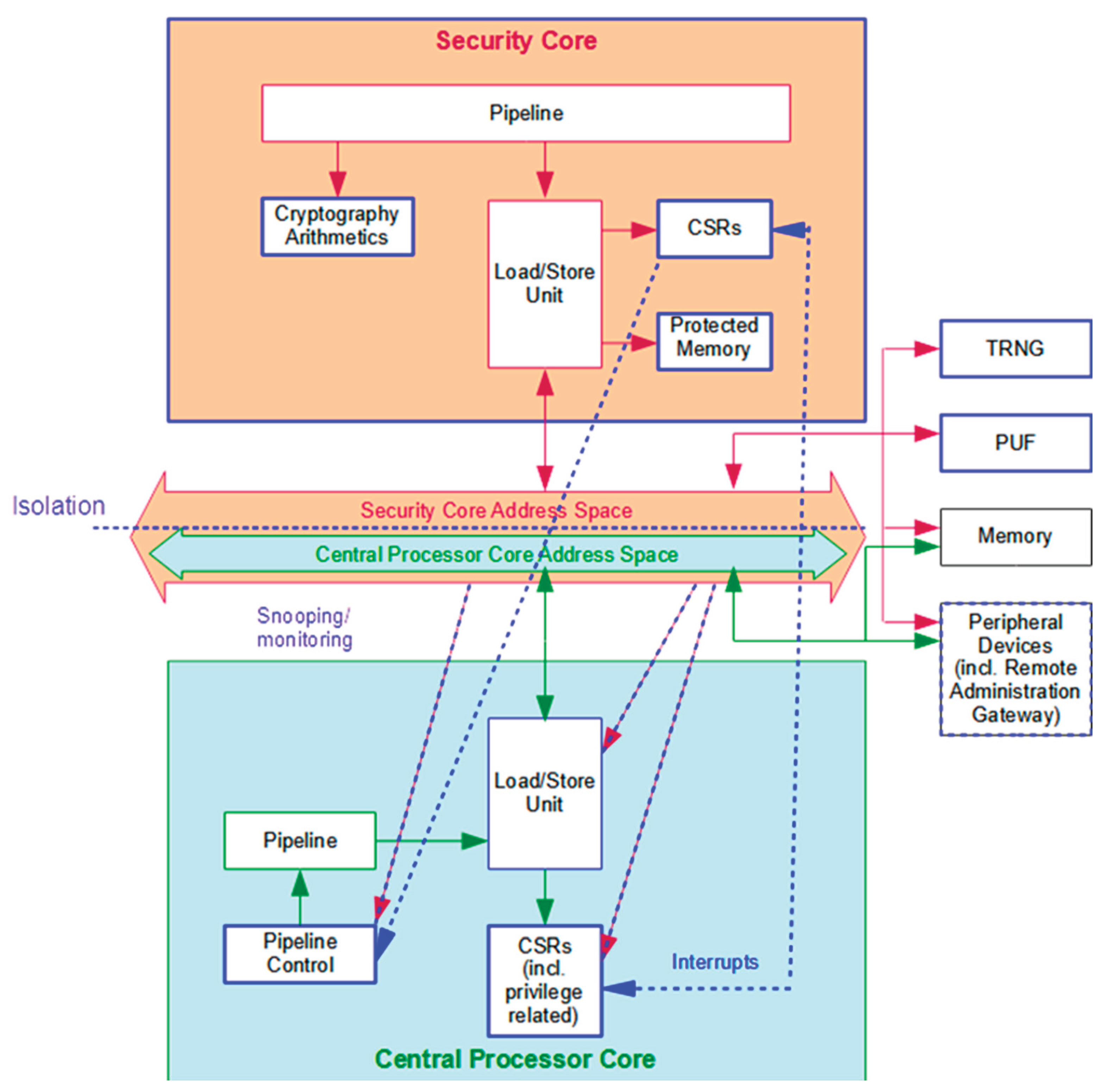
Figure 2.
Pipeline Architecture Block Diagram.
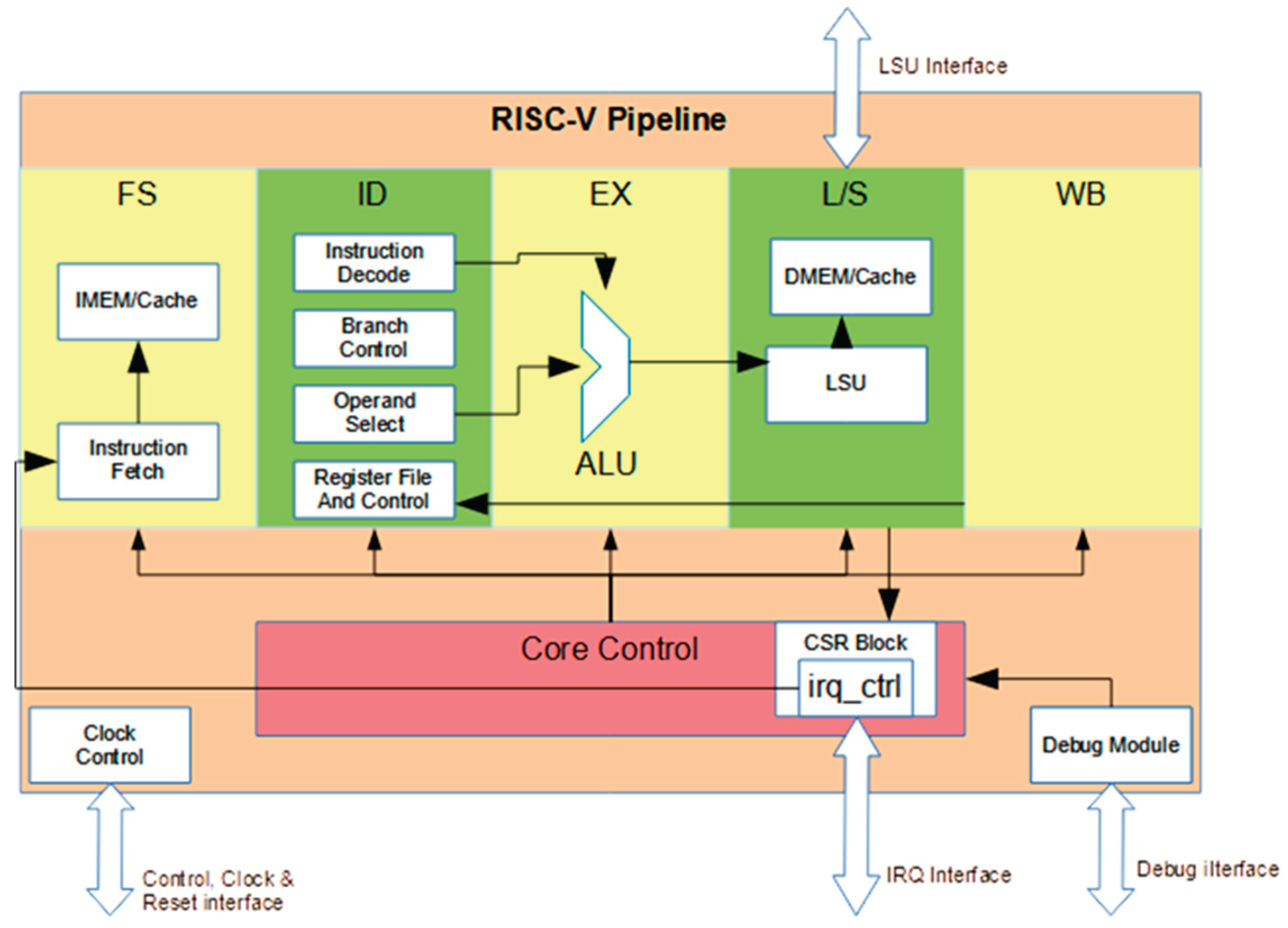
Figure 3.
Inter-System Communication.
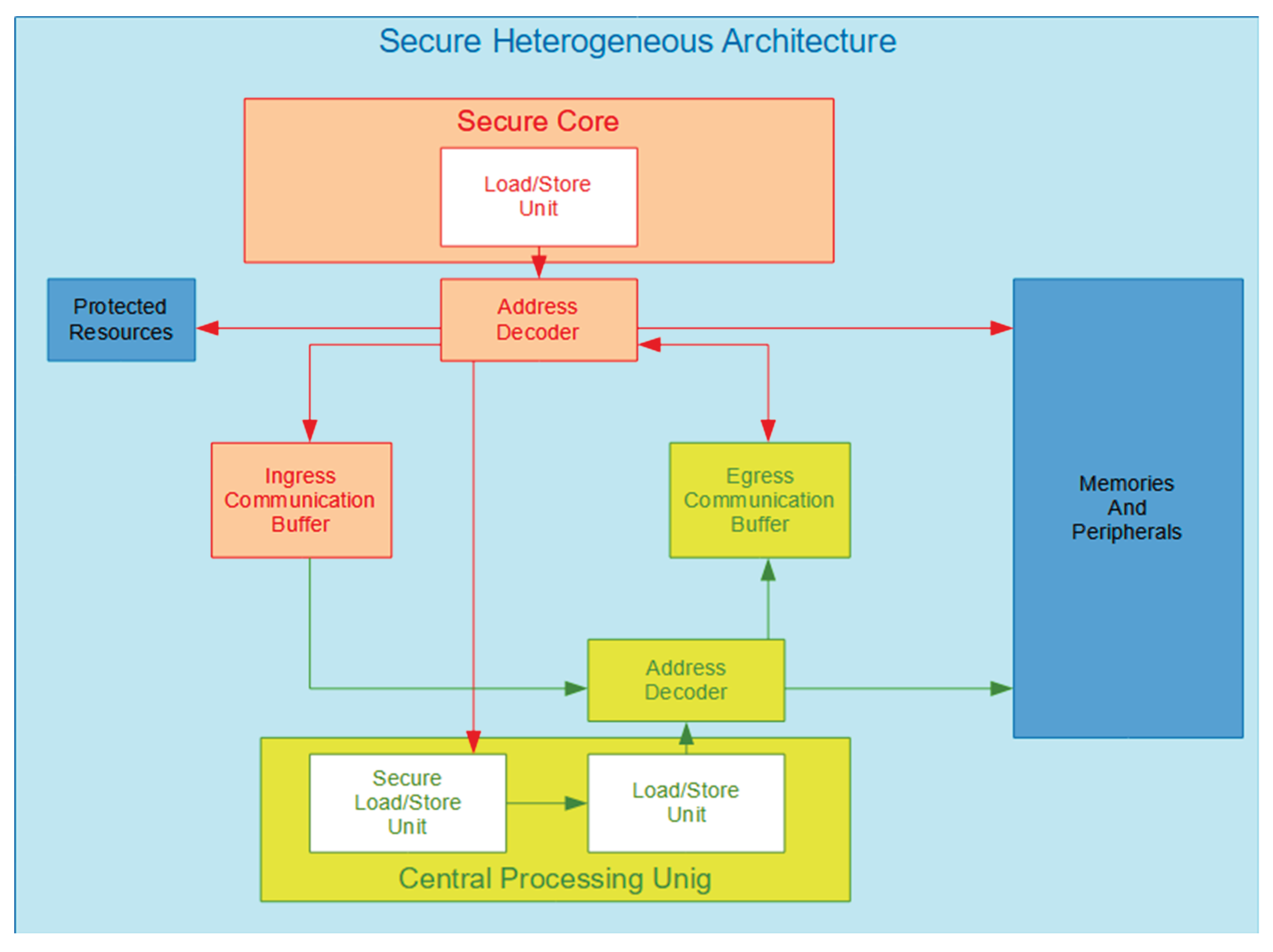
Figure 4.
Security Interface for Execution Control.
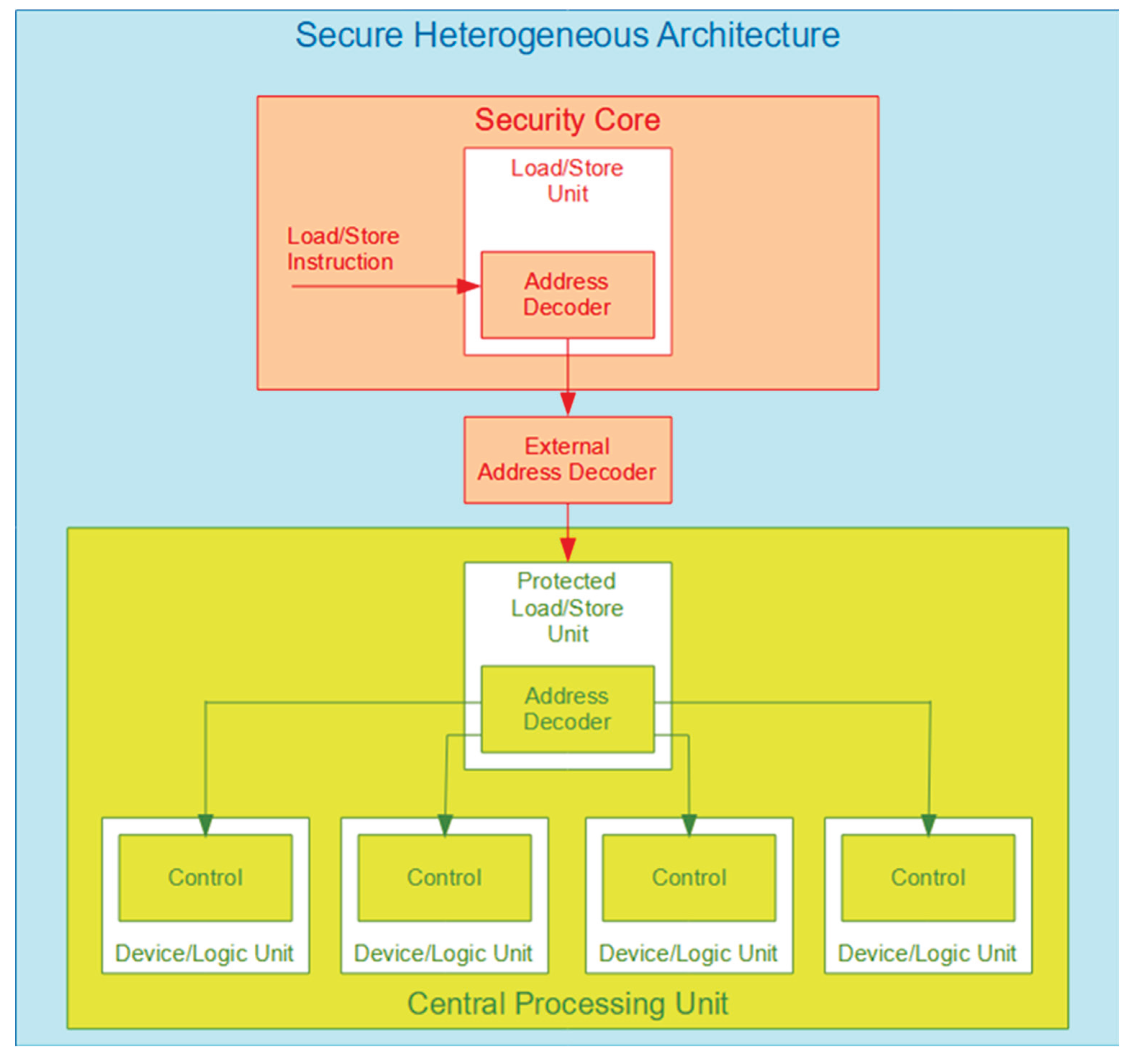
Figure 5.
Controlling CPU Program Counter.
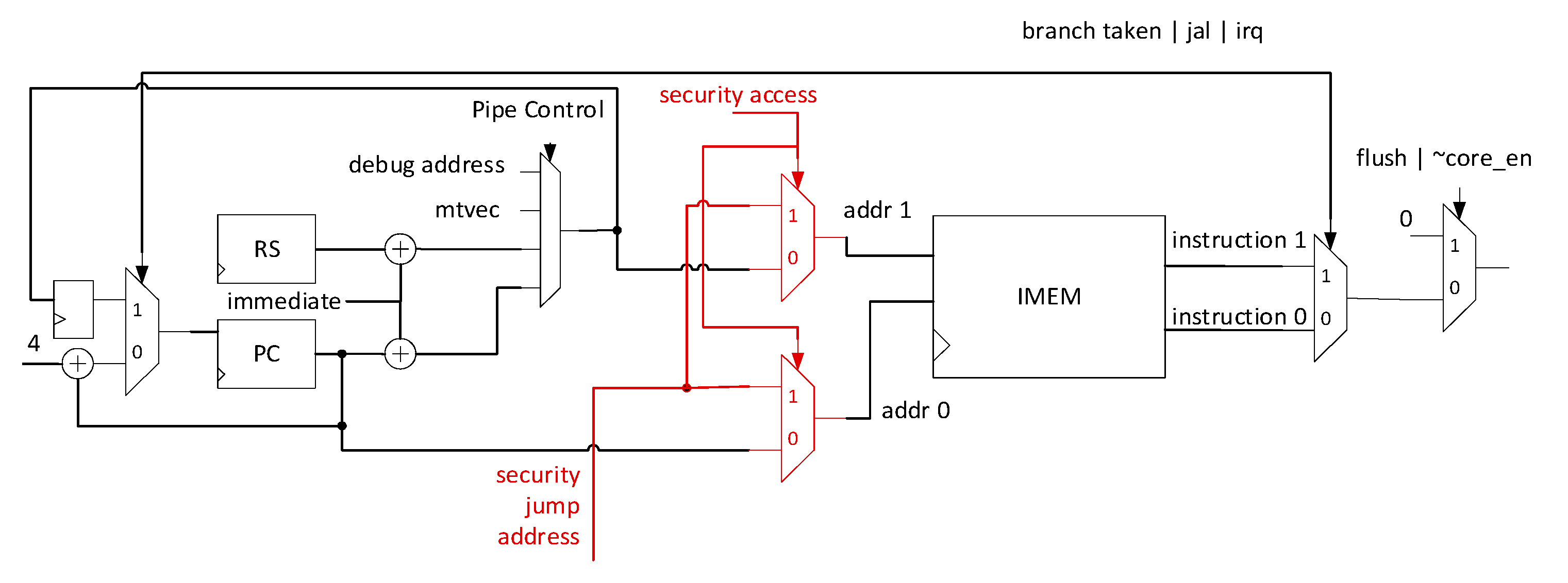
Figure 6.
Register File with two dual-port memories.
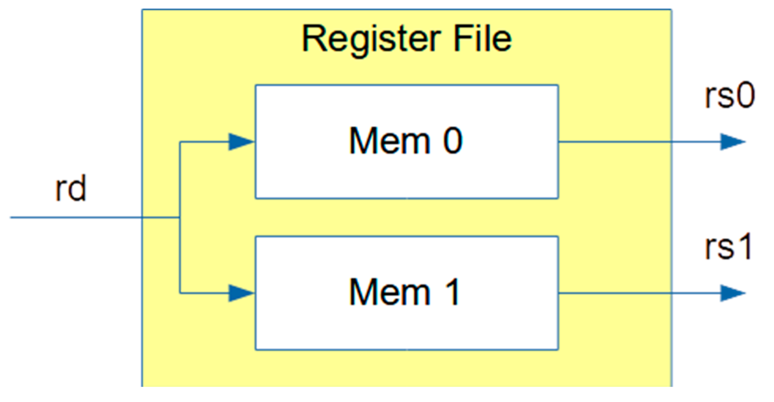
Figure 7.
Three-read port register file.
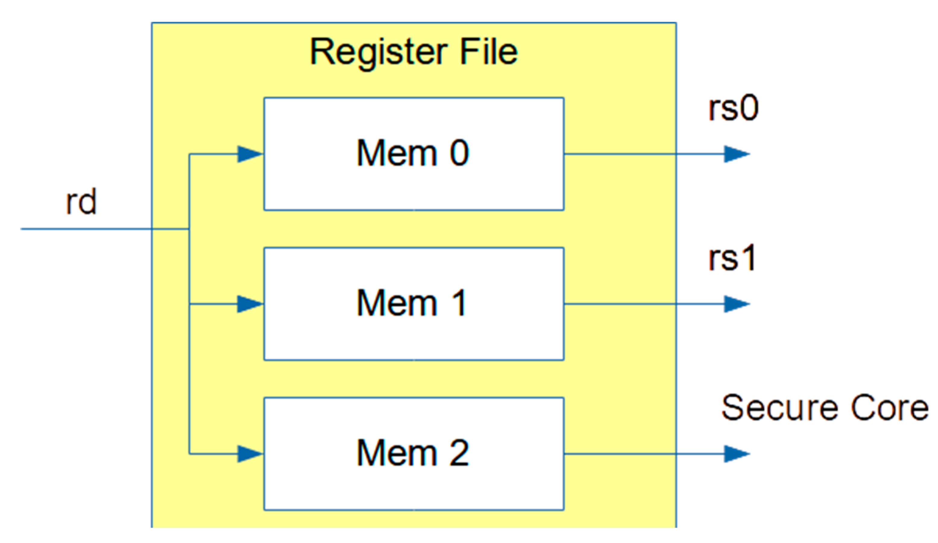
Figure 8.
Servicing concurrent CPU Load/Store Unit requests.
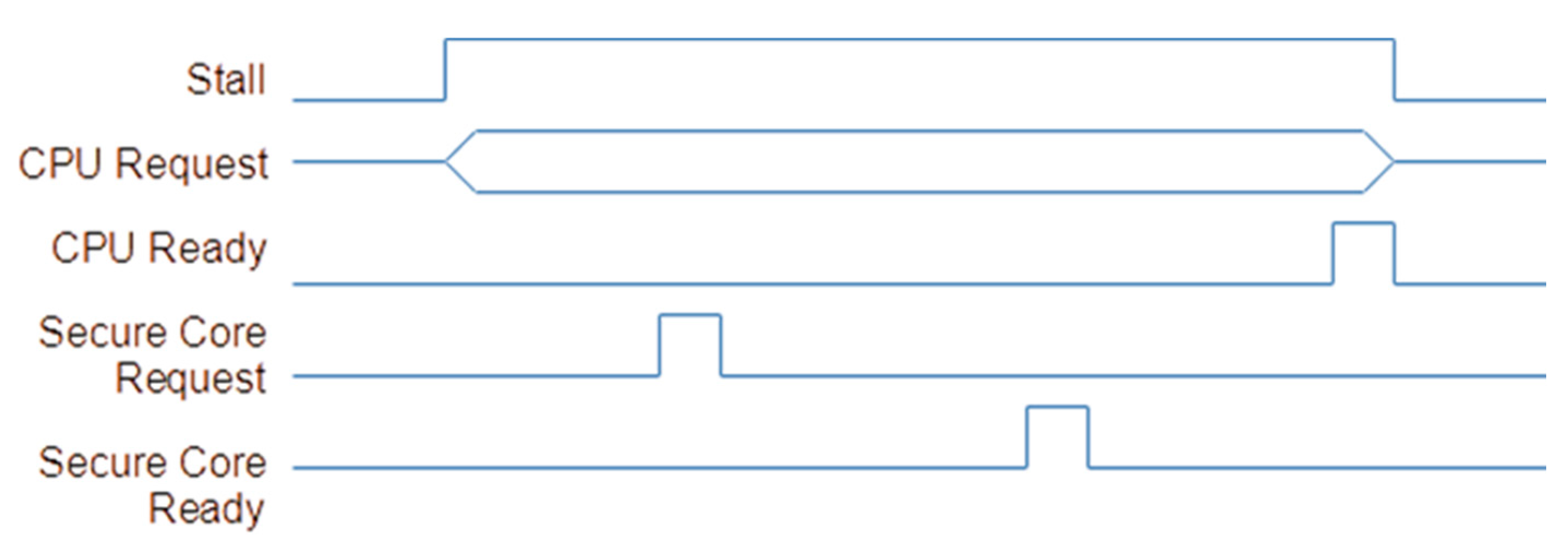

Table 1.
Security Interface signals.
| Signal | Direction | Width | Description |
| sec_if_req | Sec -> CPU | 1 | Secure Core requests CPU resource access |
| sec_if_rdy | CPU -> Sec | 1 | CPU response – immediate on write, with read data on read |
| sec_if_we | Sec -> CPU | 1 | Write enable |
| sec_if_addr | Sec -> CPU | 32 | Address to decode a CPU resource |
| sec_if_wdata | Sec -> CPU | 64 | Write data |
| sec_if_rdata | CPU -> Sec | 64 | Muxed read data |
Table 2.
Secure Core decoded address bits.
| Address bits | Value | Decoded Resource |
| 25:24 | 0 | Security Interface |
| 22:20 | 0 | CPU Program Counter |
| 22:20 | 1 | CPU Instruction Memory |
| 22:20 | 2 | CPU Load/Store Unit |
| 22:20 | 3 | CPU CSRs |
| 22:20 | 4 | CPU Register File |
| 19:18 | 2 | External Core Interface |
Table 3.
Monitored points effectiveness.
| Component | Performance Impact (for Reads) | Additional Logic | Component | Performance Impact (for Reads) | ||
| Program Counter Instruction Memory Register File |
None | Minimal | Advisory to halt CPU | Minimal * | ||
| Need to halt CPU | Minimal | Need to halt CPU | Minimal | |||
| None | Some | Need to halt CPU | Minimal | |||
| CSRs Load/Store Unit |
None | Minimal | None | Minimal | ||
| Depends on simultaneous software access probability | Minimal | Depends on simultaneous software access probability | Minimal | |||
| Program Counter Instruction Memory Register File CSRs |
None | Minimal | Advisory to halt CPU | Minimal * | ||
| Need to halt CPU | Minimal | Need to halt CPU | Minimal | |||
| None | Some | Need to halt CPU | Minimal | |||
| None | Minimal | None | Minimal | |||
| Load/Store Unit Program Counter |
Depends on simultaneous software access probability | Minimal | Depends on simultaneous software access probability | Minimal | ||
| None | Minimal | Advisory to halt CPU | Minimal * | |||
| Instruction Memory | Need to halt CPU | Minimal | Need to halt CPU | Minimal |
*Program Counter logic is typically a timing bottle neck, so even minimal logic might be critical.
Disclaimer/Publisher’s Note: The statements, opinions and data contained in all publications are solely those of the individual author(s) and contributor(s) and not of MDPI and/or the editor(s). MDPI and/or the editor(s) disclaim responsibility for any injury to people or property resulting from any ideas, methods, instructions or products referred to in the content. |
© 2026 by the authors. Licensee MDPI, Basel, Switzerland. This article is an open access article distributed under the terms and conditions of the Creative Commons Attribution (CC BY) license (http://creativecommons.org/licenses/by/4.0/).
Copyright: This open access article is published under a Creative Commons CC BY 4.0 license, which permit the free download, distribution, and reuse, provided that the author and preprint are cited in any reuse.


