Submitted:
15 December 2025
Posted:
17 December 2025
You are already at the latest version
Abstract
Hardware-in-the-Loop (HIL) simulation has become an indispensable tool for rapid and cost-effective development and validation of power electronic systems. This paper presents a detailed experimental characterization and validation of a PLECS-based HIL model for a Dual Active Bridge (DAB) DC-DC converter controlled using Single Phase Shift (SPS) modulation. An extensive experimental investigation is conducted to characterize the converter's performance across a wide range of operating conditions. The primary objective of this work is to validate and fine-tune the PLECS-based HIL model of a single DAB converter, laying the foundation for building more complex models, such as configurations with multiple converters connected in series or parallel. A DAB prototype has been characterized by varying the PWM phase shift angle between the input-output full-bridges over a range of equivalent input-output voltage levels. The power flow and efficiency were also analyzed at different voltage gains (M = 0.6, 1, and 1.4). In addition, the influence of key parameters like switching frequency and leakage inductance on the converter’s power flow and efficiency was experimentally evaluated. The experimental efficiency trends and power characteristics across the operating points provide valuable insight into the optimal modulation range and loss mechanisms of the DAB converter under SPS control. The HIL model is thoroughly tested against the experimental hardware prototype by comparing key metrics, including transferred power and system efficiency. The results demonstrate a high degree of accuracy between the HIL model and the physical system across all tested operating conditions. This work provides a validated, high-fidelity HIL model and a comprehensive dataset that confirms the effectiveness of the PLECS platform for the development and optimization of DAB converters, thereby reducing design time and mitigating risks in subsequent prototyping stages.
Keywords:
Dual Active Bridge (DAB)
; Hardware in the Loop (HIL)
; PLECS RT Box
; Single Phase Shift (SPS) modulation
; efficiency
; power flow characterization
; DC-DC converter
; voltage gain
1. Introduction
In recent years, the introduction of Renewable Energy Sources (RES), such as photovoltaics and fuel cells, has been actively promoted as a means of addressing environmental issues. To accelerate the use of RES, independent distribution systems, often defined as micro or nanogrids, have become a solution for overcoming the power fluctuations of RES. Among them, the DC MicroGrid is gaining rapid attention from researchers as an auxiliary solution to the existing power network, as it facilitates the integration of Battery Energy Storage Systems (BESS) and EV fleets [1,2].
In a DC microgrid, converting power between different voltage levels requires features such as high-power density and bidirectional power flow. Additionally, when interconnecting a medium-voltage bus to a low-voltage bus, galvanic isolation becomes essential. This is to avoid the propagation of fault and improve the grid safety, as well as giving the possibility to maintain two different grounding schemes. The isolation can be achieved by utilizing High Frequency Transformers (HFT) due to their light weight and low volume. Thus, isolated bi-directional DC-DC converters, utilizing fast switching semiconductor devices, are considered as the most suitable candidates to provide an interlink between DC buses operating at different voltage levels [3]. Figure 1 shows a general block diagram of a DC microgrid, where a DC-DC converter is employed for providing a link between two DC buses for power flow regulation.
Various isolated DC–DC converters have been investigated in the literature for bidirectional operation. Among them, the DAB converter poses to be an ideal solution because of its unique features, such as a wide range of operating voltages (high voltage gain), a wide Zero Voltage Switching (ZVS) region, bidirectional power transfer, high power density, enhanced power flow capability, and galvanic isolation. In addition, DAB contains fewer components than resonant converters and forms an integral part of a solid-state transformer or smart transformer [4].
Various control techniques are proposed in the literature for regulating the performance of conventional DAB, each having its own advantages and limitations [5]. The modulation schemes of DAB converters can be mainly classified into four kinds according to the control variables or the degrees of control freedom. The simplest method with only one control freedom to control the output power of DAB converters is Single Phase Shift (SPS) modulation [6,7] that controls the phase shift ratio between the primary side full bridge and the secondary side full bridge. It has high efficiency at full load and a unity voltage conversion ratio, due to ZVS. However, when there is a deviation of the voltage conversion ratio from unity, especially at light load, it loses ZVS and undergoes hard switching, thus leading to increased switching losses. Moreover, it also increases reactive power (circulating power) and current stress, which reduces its efficiency. To overcome the aforementioned limitations, Extended Phase Shift (EPS) [8,9] and Dual Phase Shift (DPS) [10,11] techniques were proposed. For the EPS modulation scheme, the internal phase-shift duty ratio of one full bridge can be adjusted additionally. Similarly, by modifying the SPS control, the DPS modulation scheme can regulate the internal phase-shift duty ratios of both full bridges for the DAB converter with the same value. Both EPS and DPS modulation schemes have two control variables. The Triple Phase Shift (TPS) modulation scheme [12,13,14], which controls the duty ratios of two full bridges and the phase shift ratio between them individually, facilitates the greatest degree of control freedom with the constant switching frequency. Hence, SPS control, EPS control, and DPS control can be considered as special cases of TPS control.
Typically, the first step in developing a physical prototype of a power electronic converter for a particular application is to verify the feasibility and the basic technical characteristics of the proposed concept. For these purposes, various computer simulation tools are used to simulate the electrical behavior of the converter. Two main approaches are commonly used to simulate the power section and control system of the converter. The first (also traditional) approach is the implementation of only off-line simulation, also known as Software-In-the-Loop (SIL) simulation, while the second one involves on-line simulation using the Hardware-In-the-Loop (HIL) system [15].
With the traditional approach, computer simulation programs mainly model the electrical behavior of the power section of the converter. Offline simulation experiments are followed by choosing the necessary components and the development of a physical model of the power section of the electronic converter. Thereafter, a series of laboratory tests is carried out together with a control electronic module. Errors detected during these tests usually require modifications to the converter’s power and control section, leading to several iterations of the design process. An increased number of iterations necessarily leads to higher costs and longer times of the converter design process [16]. On the other hand, in the HIL simulation approach, a physical converter prototype is not developed immediately after offline simulations of the power section. Instead, the prototype is realized only after the control electronics have been tested and verified. The model of the power section of the converter, simulated offline, is uploaded to a real-time emulator that reproduces its operation. Using its analog/digital inputs and outputs, this emulator is connected to a control electronics module with a built-in control algorithm. Especially when the converter topology is complex or multiple power-conversion stages must be interconnected, this approach accelerates the system design, making it more efficient and more cost-effective than designs based solely on offline simulations [17]. However, validation of each stage model is essential to avoid propagation of modelling errors or underestimated effects. This paper presents the key steps in designing the HIL simulation model of the DAB DC-DC converter using PLECS RT BOX 1 CE real-time power electronics emulator from Plexim, and the relative validation through an experimental prototype.
Over the years, the theory behind DAB converters and HIL simulations has been well established through a number of studies, yet one crucial area still needs to be addressed by the researchers, and that is the full experimental validation of HIL models in situations where the converter is operating in the multi-variable design space. Most of the findings of the previous studies are limited by the operational points of the models, which are usually nominal points, and variations in phase shift and power transfer are mainly considered [18,19,20,21]. On the other hand, a detailed experimental study, which at the same time investigates the impact of different parameters on power transfer and efficiency, is completely missing. This includes parameters like phase shift, voltage gain, switching frequency, inductance, and PWM duty ratio, which are central to DAB optimization. This is necessary for the precise validation of HIL models and the understanding of converter behavior in the real world. The present paper fills this gap by carrying out a very thorough, multi-faceted experimental characterization and validation of a PLECS-based HIL model of the DAB converter, systematically evaluating converter performance across a wide matrix of operating conditions, thus providing valuable insight into its steady-state and efficiency characteristics.
The rest of this paper is structured as follows: Section II presents the operational principle of a DAB converter, while Section III talks about the basics of DAB HIL setup in PLECS. Furthermore. Section IV shows the experimental testbench and different characterizations performed on the DAB converter. The multi-variable comparative results derived from both the HIL setup and experiments are also presented in this section, and the work is concluded in Section V.
2. Operating Principle of DAB Converter Under SPS Modulation
The simplicity of SPS modulation makes it the most widely used power flow control technique for the DAB converter. The basic topology of a DAB converter is shown in Figure 2. It is composed of two full-bridge converters, an isolating HFT, and an energy storage inductor, which could be an external inductor or the lumped leakage inductor of the transformer.
As shown in Figure 2, the converter’s two H-bridges (full bridges) transform the DC input and output voltages into high-frequency 2-level square waves (V1 and V2). We can control the power flow by adjusting the phase shift between these square waves using SPS. Figure 2 shows the possible directions of power flow (positive or negative). The direction depends on the sign of the phase shift angle. A positive angle means V2 lags behind V1, resulting in positive power flow. On the contrary, a negative angle means that V1 lags behind V2, leading to negative power flow. Figure 3 shows typical steady-state operational waveforms for a DAB converter operating in buck mode (Vin > Vout) with positive power flow using SPS modulation. In this mode, both bridges operate at the same switching frequency with a 50% duty cycle [22,23,24].
By ignoring the resistive losses in the converter, the average transmitted power can be expressed by (1), where fs is the switching frequency of the converter, and L is the equivalent inductance and given by (2). In (2), Ltr1 and Ltr2 are respectively the leakage inductances of the primary and secondary sides of the HFT, while Ls is the additional series inductance.
According to (1), the magnitude of the power transferred in the positive direction increases as the phase shift angle (φ) increases up to a maximum at π/2, after which any increase in phase shift angle causes a decrease in power sent. A similar pattern is found in the reverse direction, with the highest reverse power obtained at -π/2.
3. Hardware-in-the-Loop Modelling of DAB Converter Using PLECS
In HIL testing, the DAB power converter with the load represents the physical Device Under Test (DUT) and is therefore the plant. This plant model is implemented in the RT BOX 1 CE power electronics emulator from Plexim with a PLECS circuit simulator. The control algorithm is implemented in an STM32F446RE microcontroller development board from ST-Microelectronics. The physical connection between RTBOX CE and the STM32 microcontroller is provided by the interface boards, thus enabling real-time emulation of the DAB power stage. These boards connect and protect the input-output pins between the microcontroller and the RTBOX CE. Figure 4 shows the block diagram of HIL testing.
During the development of the HIL simulation model, both the physical limitations of RTBOX CE hardware and the need for optimization to improve simulation accuracy must be carefully considered. One key optimization step involves employing either sub-cycle averaging or nanostep models of the switching devices in combination with the PWM Capture components implemented on the RTBOX CE FPGA. This real-time optimization strategy enables the use of smaller simulation time steps and allows the evaluation of significantly higher converter switching frequencies. Furthermore, with an appropriate choice of discretization time step, the PLECS hybrid power modules can accurately depict the main switching ripple characteristics of the converter and reduce the number of ideal switches and diodes in the model, which lowers the quantity of state-space matrices needed to describe a power converter. With these optimizations, a reduction of the computational load of real-time simulations can be achieved. The plant model of the DAB HIL setup in the PLECS environment is shown in Figure 5.
4. Experimental Setup, Characterization, and Results
An experimental prototype of the DAB converter was assembled as shown in Figure 6. The converter uses a motherboard that hosts four half-bridges implemented with wide-bandgap GaN power transistors from EPC (EPC23102). GaN devices were selected to enable higher switching frequencies while keeping dynamic switching losses low, which is particularly advantageous for the low DC-link voltages targeted in this work (≤ 50 V). Two ITECH IT-M3902C-85-40SAS bidirectional power supplies were used to set the input and output voltages of the DAB converter. The experimental setup also includes an oscilloscope (Teledyne LeCroy WaveSurfer 3024z) for monitoring PWM switching waveforms, currents, and voltages, as well as auxiliary fans for active cooling. A FLIR A325 thermal imaging camera was employed to detect any potential overheating during the tests. Particular attention was given to the GaN power transistors, inductors, and transformers, as these are the components most subject to heat dissipation. Table 1 shows the converter specifications adopted for the initial tests. The converter control and characterization were done using an STM32F446RE development board.
The results of the power transfer and efficiency obtained for different series inductors’ inductances (L), voltages, and switching frequencies (fsw) when the converter normalized gain is M = Vout/(n×Vin) = 1 (i.e., in this case, Vout = Vin) are shown in Figure 7 and Figure 8. As outlined in Figure 7, four different configurations were tested: (a) a single 10 µH inductor at 100 kHz; (b) a parallel combination of three 33 µH inductors (resulting in an effective inductance value of 11 µH ) at 50 kHz; (c) the same 11 µH parallel inductor bank at 100 kHz; and (d) a parallel combination of two 10 µH inductors (resulting in 5 µH ) at 200 kHz. These variations allow for the analysis of the impact of the characteristic impedance Z = jωL (where ω = 2πfsw, and ) on power transfer, soft-switching, and overall efficiency.
All the curves in Figure 7 show that for any given phase shift, the magnitude of the power transfer increases proportionally as the voltages increase from 10 V to 48 V, confirming the direct relationship between power flow and voltage amplitude according to equation (1). Moreover, the power curves at all the voltages increase as the phase shift increases, with the peak power occurring when the normalized phase shift is 0.5. Also noticeable is that the power transfer curves of Figure 7a and Figure 7d are nearly identical despite the different inductances and switching frequencies. This is because both configurations have the same characteristic impedance (i.e., their reactances are Xa = ωaLa = 2π×100×103×10×10–6 = 2π Ω and Xd = ωdLd = 2π×200×103×5×10–6 = 2π Ω). If we compare all four plots at 20 V, it is observed that Figure 7b provides the largest power transfer simply because its characteristic impedance is the smallest, i.e., Xb = ωbLb = 2π×50×103×11×10–6 = 2π×0.55 Ω.
The efficiency curves of Figure 8 show that at a particular voltage, efficiency increases as power demand increases up to an optimal point, after which efficiency drops. As we move from one voltage level to the other, the zone of higher efficiency changes. In all cases, the light load efficiency is highest when the voltage is smallest due to lower switching losses, while the heavy load efficiency is highest when the voltage is largest. The efficiency curves of Figure 8d are higher than those of Figure 8a, mainly because the DC resistance of the inductor is lower (1 mΩ // 1 mΩ = 0.5 mΩ), hence the conduction losses are reduced.
An extraction of the maximum power and efficiency points at different voltages for the case given in Figure 7a and Figure 8a gives the plot shown in Figure 9, where it is clearly seen that as the input/output voltage increases, the maximum efficiency increases up to a maximum of 96% when the voltage is 48 V.
Figure 10 shows the DAB power transfer and efficiency curves when the DAB converter is characterized at different gain values of M = 0.6 (Vin = 30 V, Vout = 18 V), M = 1 (Vin = 30 V, Vout = 30 V), and M = 1.4 (Vin = 30 V, Vout = 42 V). It is observed in Figure 10a that as the gain increases, more power can be transferred for every increase in the phase shift. Moreover, Figure 10b shows that the efficiency of the converter at light load is higher when the converter gain is lowest (M = 0.6), whereas the efficiency at heavy load is highest when the converter gain is highest, and finally, at medium loads, the efficiency is highest when M = 1.
The efficiency trends in Figure 10b can be explained by the distribution of conduction and switching losses at different operating points. Operating at light load with a lower gain (M = 0.6) minimizes circulating current and core excitation, leading to reduced conduction and magnetizing losses and therefore higher efficiency. At heavy load, however, a higher gain (M = 1.4) reduces the required phase shift to deliver the same power, which lowers RMS currents and conduction losses, improving efficiency. At medium loads, the system operates closest to its nominal design point when M = 1, balancing both conduction and switching losses and resulting in the highest efficiency at that gain level.
Figure 11 shows a power flow comparison of the HIL setup with the experimental setup under different operating conditions.
It can be observed that at all operating conditions tested, the HIL model accurately reproduces the power-flow behavior of the converter for positive phase-shift values. In this region, the HIL and experimental curves exhibit nearly parallel trends, with power scaling consistently with the applied voltage, and both traces closely following the same power envelope as a function of phase shift. For negative phase shifts, the HIL model remains accurate at low power levels. However, as the transferred power increases, a modest deviation emerges between the HIL predictions and the measured responses, with the greatest difference being when M = 1.4. This discrepancy can be attributed to the non-idealities of the real prototype not modelled in the HIL model, such as transformer parasitics, dead-time effects, magnetizing inductance, and switching nonlinearities, which become increasingly significant at high power levels. Overall, the proposed HIL model provides a robust and reliable representation of the physical system and is therefore suitable for further control development and testing.
5. Conclusions
This paper presents a validated, high-fidelity PLECS-based HIL simulation methodology for the development and validation of DAB converters controlled with SPS modulation. Through systematic experimental characterization across a broad range of operating points including multiple voltage levels (10 V, 20 V, 30 V, and 48 V), voltage gains (M = 0.6, 1, and 1.4), switching frequencies, and leakage inductances, we demonstrate that the HIL model reproduces the measured power-transfer trends with close agreement under both nominal and extended conditions. The detailed comparison between HIL simulations and experimental measurements validates the suitability of this approach for rapid prototyping and control validation. A modest divergence at the higher converter gains highlights the limitations of idealized device models and switching approximations and points to clear opportunities for improvement by incorporating more detailed device characterization (for example, non-ideal switch transitions, device parasitics, and thermal effects) and communication/timing jitter into the HIL model.
The comprehensive dataset generated during this investigation confirms that PLECS RT Box platforms, when properly interfaced with real-time DSP controllers like STM32F4466RE, can reliably emulate the DAB’s dynamic behavior in real time, thus providing a reliable, cost-effective, and lower risk alternative to hardware prototyping for DAB converter design and optimization.
Overall, this work establishes a validated foundation for future research, for instance, advanced modulation strategies, multi-port DAB architectures, and real-time fault or stress analysis within high-power conversion systems, and demonstrates that the methodologies and validation approaches presented are transferable to other power-conversion topologies. Consequently, the proposed HIL workflow can help designers shorten development cycles and reduce prototyping risk in modern power-electronics systems.
Author Contributions
Conceptualization, Armel Asongu Nkembi and Danilo Santoro; methodology, Armel Asongu Nkembi and Danilo Santoro; software, Armel Asongu Nkembi; validation, Armel Asongu Nkembi and Danilo Santoro; formal analysis, Armel Asongu Nkembi; investigation, Armel Asongu Nkembi and Danilo Santoro; resources, Danilo Santoro; data curation, Armel Asongu Nkembi; writing—original draft preparation, Armel Asongu Nkembi; writing—review and editing, Danilo Santoro, Nicola Delmonte and Paolo Cova; visualization, Danilo Santoro; supervision, Nicola Delmonte; project administration, Paolo Cova; funding acquisition, Paolo Cova. All authors have read and agreed to the published version of the manuscript.
Funding
This research was funded by the “National Recovery and Resilience Plan (NRRP), Mission 4 Component 2 Investment 1.5—Call for tender No. 3277 of 30 December 2021 of Italian Ministry of University and Research funded by the European Union—NextGenerationEU. Project code: ECS00000033, Concession Decree No. 1052 of 23 June 2022 adopted by the Italian Ministry of University and Research, CUP D93C22000460001, Project title: Ecosystem for Sustainable Transition in Emilia-Romagna”.
Data Availability Statement
No new data were created or analyzed in this study. Data sharing is not applicable to this article.
Acknowledgments
The authors acknowledge the use of Microsoft Copilot (GPT-5 model) during the preparation of this manuscript for assistance in refining text. The authors have reviewed and edited all AI-generated content and take full responsibility for the final version of the publication.
Conflicts of Interest
The authors declare no conflicts of interest.
Abbreviations
The following abbreviations are used in this manuscript:
| DAB | Dual Active Bridge |
| HIL | Hardware-in-the-Loop |
| SPS | Single Phase Shift |
| EPS | Extended Phase Shift |
| DPS | Dual Phase Shift |
| TPS | Triple Phase Shift |
| PWM | Pulse Width Modulation |
| RES | Renewable Energy Sources |
| BESS | Battery Energy Storage Systems |
| EV | Electric Vehicle |
| HFT | High Frequency Transformer |
| SIL | Software-in-the-Loop |
| DUT | Device Under Test |
| RT BOX | Real-Time Box (Plexim hardware) |
| GaN | Gallium Nitride |
References
- Y. Eto, Y. Noge, M. Shoyama and T. Babasaki, "Stability Analysis of Bidirectional Dual Active Bridge Converter With Input and Output LC Filters Applying Power-Feedback Control," in IEEE Transactions on Power Electronics, vol. 38, no. 3, pp. 3127-3139, March 2023. [CrossRef]
- S. Ghosh, D. Das, B. Singh, S. Janardhanan and S. Mishra, "Frequency-Domain Modeling of Dual-Active-Bridge Converter Based on Harmonic Balance Approach," in IEEE Journal of Emerging and Selected Topics in Industrial Electronics, vol. 3, no. 1, pp. 166-176, Jan. 2022. [CrossRef]
- D. Yadeo and P. Chaturvedi, "Performance Characterization of T-Type Multilevel Dual Active Bridge DC-DC Converter," in IEEE Transactions on Industry Applications, vol. 59, no. 2, pp. 1877-1886, March-April 2023. [CrossRef]
- C. Yu et al., "High Efficiency Bidirectional Dual Active Bridge (DAB) Converter Adopting Boost-Up Function for Increasing Output Power," in IEEE Transactions on Power Electronics, vol. 37, no. 12, pp. 14678-14691, Dec. 2022. [CrossRef]
- A. Tong, L. Hang, G. Li, X. Jiang and S. Gao, "Modeling and Analysis of a Dual-Active-Bridge-Isolated Bidirectional DC/DC Converter to Minimize RMS Current With Whole Operating Range," in IEEE Transactions on Power Electronics, vol. 33, no. 6, pp. 5302-5316, June 2018. [CrossRef]
- T. -Q. Duong and S. -J. Choi, "Deadbeat Control with Parameter Identification under Single Phase-Shift Modulation for Dual Active Bridge Converters," 2022 IEEE Applied Power Electronics Conference and Exposition (APEC), Houston, TX, USA, 2022, pp. 1222-1227. [CrossRef]
- Duong, Tan-Quoc, Hoai-An Trinh, Kyoung-Kwan Ahn, and Sung-Jin Choi. 2024. "Adaptive Extended State Observer for the Dual Active Bridge Converters" Sensors 24, no. 8: 2397. [CrossRef]
- F. Bagheri, N. Guler, H. Komurcugil and S. Bayhan, "An Adaptive Sliding Mode Control for a Dual Active Bridge Converter With Extended Phase Shift Modulation," in IEEE Access, vol. 11, pp. 91260-91274, 2023. [CrossRef]
- X. Li, X. Zhang, F. Lin, C. Sun and K. Mao, "Artificial-Intelligence-Based Hybrid Extended Phase Shift Modulation for the Dual Active Bridge Converter With Full ZVS Range and Optimal Efficiency," in IEEE Journal of Emerging and Selected Topics in Power Electronics, vol. 11, no. 6, pp. 5569-5581, Dec. 2023. [CrossRef]
- S. Bal, D. B. Yelaverthi, A. K. Rathore and D. Srinivasan, "Improved Modulation Strategy Using Dual Phase Shift Modulation for Active Commutated Current-Fed Dual Active Bridge," in IEEE Transactions on Power Electronics, vol. 33, no. 9, pp. 7359-7375, Sept. 2018. [CrossRef]
- Z. Guo and M. Li, "An Optimized DPS Control Strategy for LCL Resonant Dual Active Bridge Converter for Wide Voltage Conversion Ratio," in IEEE Journal of Emerging and Selected Topics in Industrial Electronics, vol. 2, no. 4, pp. 501-512, Oct. 2021. [CrossRef]
- S. M. Akbar, A. Hasan, A. J. Watson and P. Wheeler, "FEA Based Transformer Loss Analysis for Dual Active Bridge DC–DC Converter Using Triple Phase Shift Modulation," in IEEE Journal of Emerging and Selected Topics in Power Electronics, vol. 10, no. 4, pp. 4347-4360, Aug. 2022. [CrossRef]
- S. M. Akbar, A. Hasan, A. J. Watson and P. Wheeler, "Model Predictive Control With Triple Phase Shift Modulation for a Dual Active Bridge DC-DC Converter," in IEEE Access, vol. 9, pp. 98603-98614, 2021. [CrossRef]
- Y. Dai, S. Luo and Z. Li, "Direct Power Based Control Strategy for DAB DC-DC Converter With Cooperative Triple Phase Shifted Modulation," in IEEE Access, vol. 9, pp. 147791-147800, 2021. [CrossRef]
- A. Perić, H. Pauković, M. Miletić and V. Šunde, "Development of voltage source converter using HiL simulation system," 2019 42nd International Convention on Information and Communication Technology, Electronics and Microelectronics (MIPRO), Opatija, Croatia, 2019, pp. 168-173. [CrossRef]
- K. Takacs and M. Frivaldsky, "Hardware-in-the-loop modeling of three-phase T-type neutral point clamped voltage source inverter for battery charging stations," 2023 IEEE 32nd International Symposium on Industrial Electronics (ISIE), Helsinki, Finland, 2023, pp. 1-5. [CrossRef]
- G. Arena, G. Aiello, G. Scelba, M. Cacciato and F. Gennaro, "A Cost-Effective Hardware in the Loop Implementation of Dual Active Bridge for Fast Prototyping of Electric Vehicles Charging Controls," 2021 23rd European Conference on Power Electronics and Applications (EPE'21 ECCE Europe), Ghent, Belgium, 2021, pp. P.1-P.10. [CrossRef]
- Y. Xie, J. Sun and J. S. Freudenberg, "Power Flow Characterization of a Bidirectional Galvanically Isolated High-Power DC/DC Converter Over a Wide Operating Range," in IEEE Transactions on Power Electronics, vol. 25, no. 1, pp. 54-66, Jan. 2010. [CrossRef]
- Nalamati, Chandra Sekhar and Gupta, Rajesh, Frequency Domain Power Flow Characterization in Lossy Dab Converter for Battery Energy Storage. Available at SSRN: https://ssrn.com/abstract=5209443 or http://dx.doi.org/10.2139/ssrn.5209443. [CrossRef]
- J. Saelens et al., "Instantaneous Current and Average Power Flow Characterization of a DC-DC-DC Triple Active Bridge Converter," 2024 IEEE Power and Energy Conference at Illinois (PECI), Urbana, IL, USA, 2024, pp. 1-6. [CrossRef]
- M. Neubert, A. Gorodnichev, J. Gottschlich and R. W. De Doncker, "Performance analysis of a triple-active bridge converter for interconnection of future dc-grids," 2016 IEEE Energy Conversion Congress and Exposition (ECCE), Milwaukee, WI, USA, 2016, pp. 1-8. [CrossRef]
- Wang, Suhua, Fei Yu, and Jiaming Qi. 2025. "Model Predictive Voltage Control Strategy for Dual Active Bridge Converters Based on Super-Twisting Integral Sliding Mode Observer" Electronics 14, no. 8: 1496. [CrossRef]
- Henao-Bravo, Elkin Edilberto, Carlos Andrés Ramos-Paja, and Andrés Julián Saavedra-Montes. 2022. "Adaptive Control of Photovoltaic Systems Based on Dual Active Bridge Converters" Computation 10, no. 6: 89. [CrossRef]
- Flux control modulation for the dual active bridge DC/DC converter: . [CrossRef]
Figure 1.
Architecture of a possible DC microgrid.
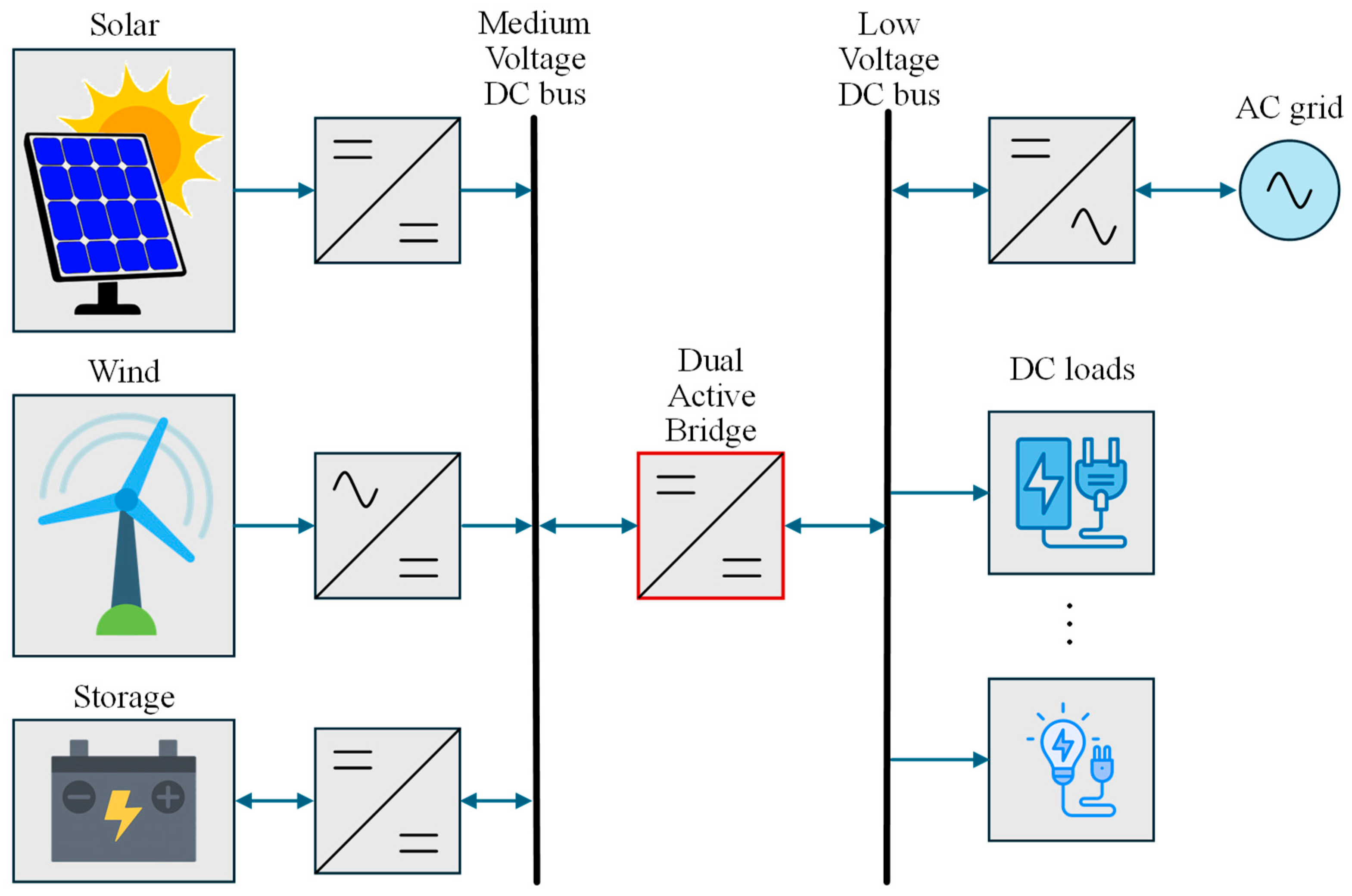
Figure 2.
Basic architecture of a DAB converter.
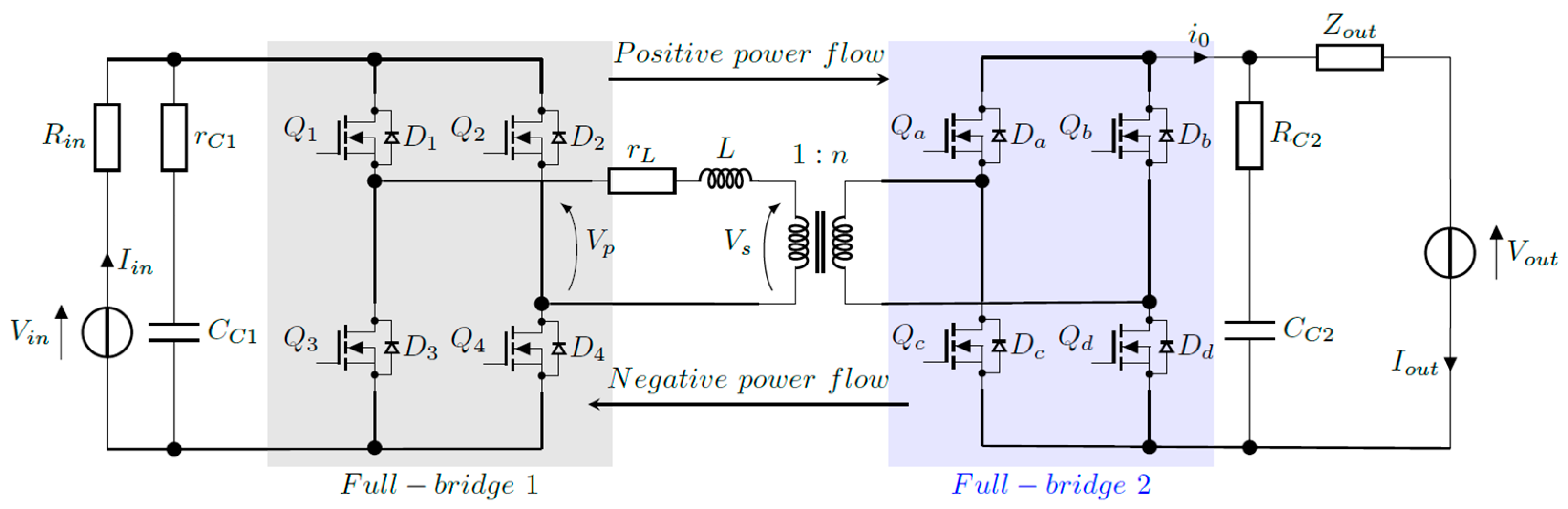
Figure 3.
Typical theoretical waveforms of the DAB converter under SPS modulation.
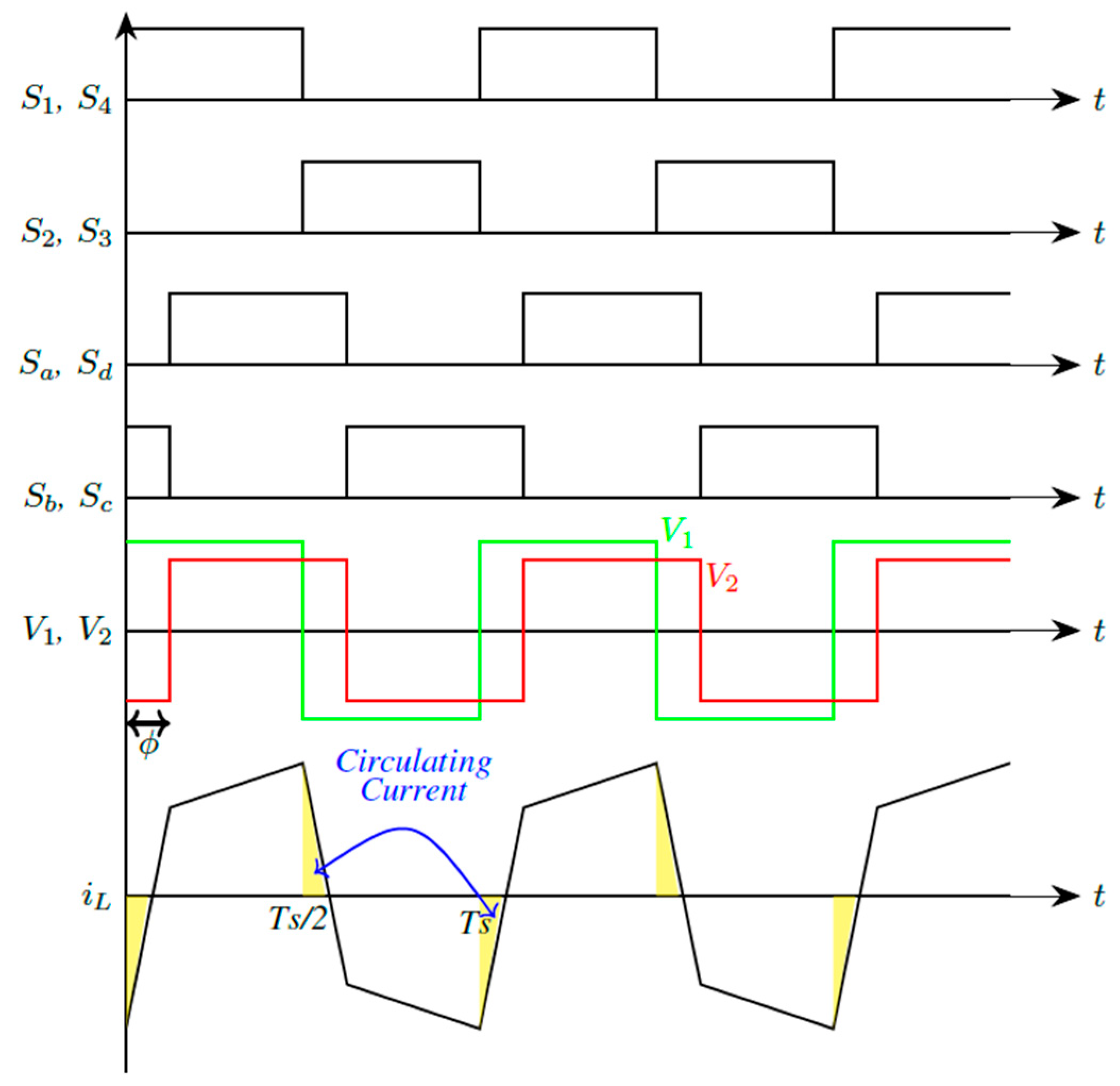
Figure 4.
Block diagram of HIL Testing.
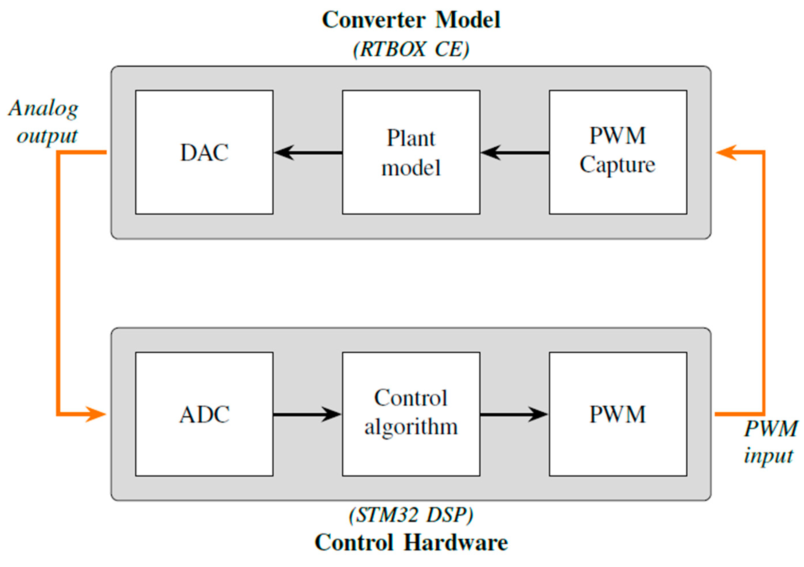
Figure 5.
Plant model of the HIL testing in PLECS.
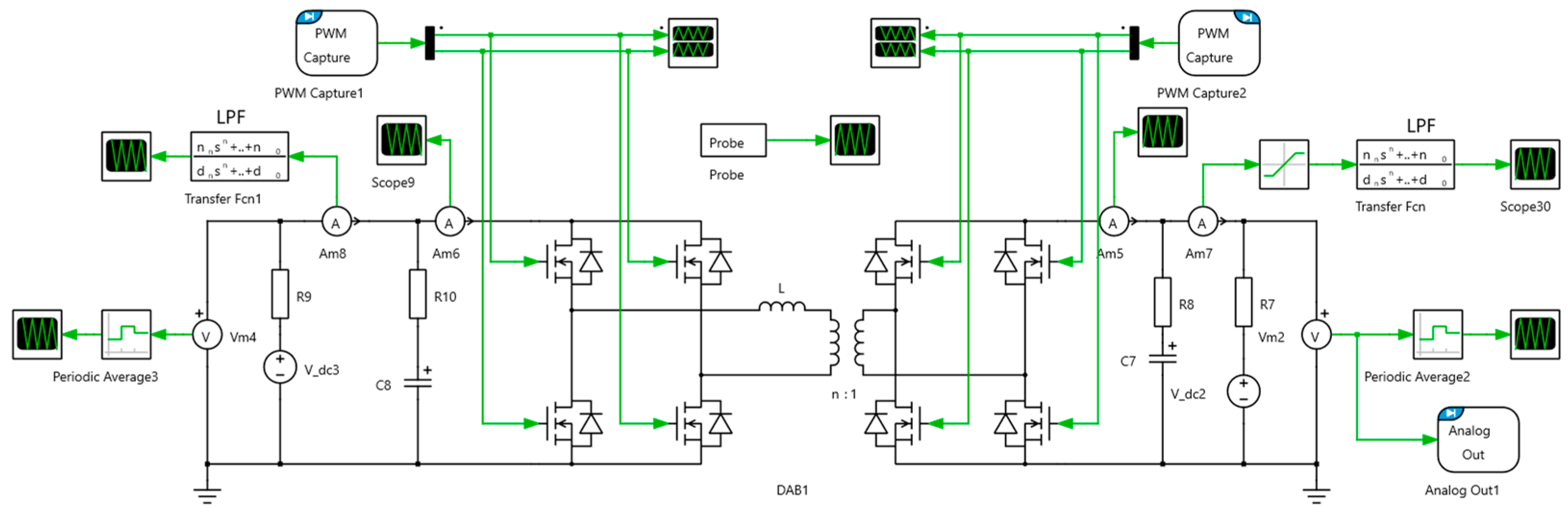
Figure 6.
Picture of the DAB experimental test bench for carrying out tests. From left to right: A) Bidirectional power supply ITECH IT-M3902C-85-40SAS, B) PC for microcontroller monitoring, C) Thermal IR camera FLIR A325, D) Multimeter FLUKE 83V, E) DAB prototype, F) PC for thermal imaging monitoring, G) Multimeter HP 34401A, H) Power supply TTI CPX400DP, I) Power supply Keysight E3646A, J) Multimeter Keysight 34450A, K) Multimeter FLUKE 45, L) Oscilloscope Teledyne LeCroy WaveSurfer 3024z.
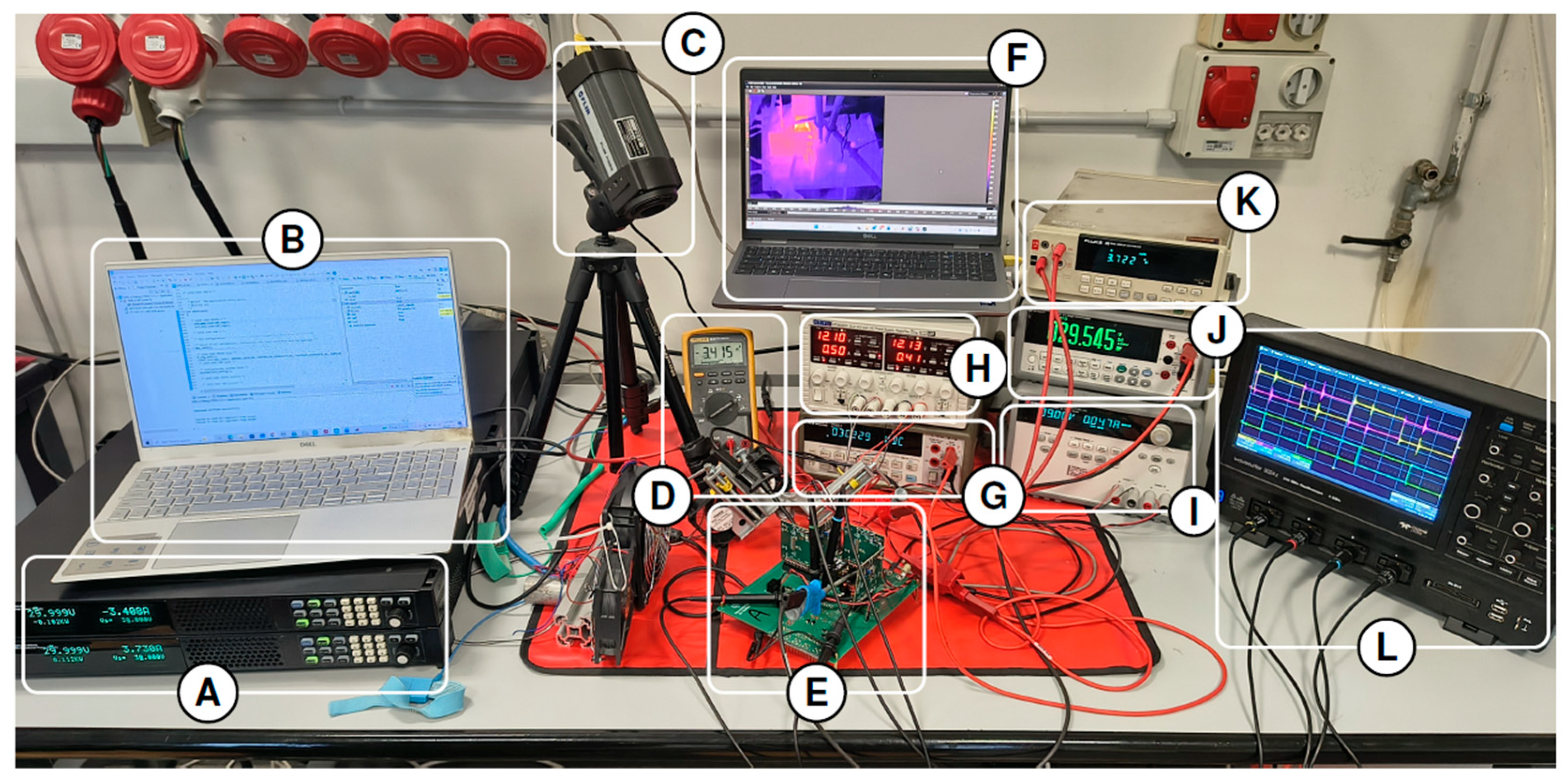
Figure 7.
Power transfer characterization at different voltages, frequencies, and inductances, V = n×Vin = Vout.
Figure 7.
Power transfer characterization at different voltages, frequencies, and inductances, V = n×Vin = Vout.
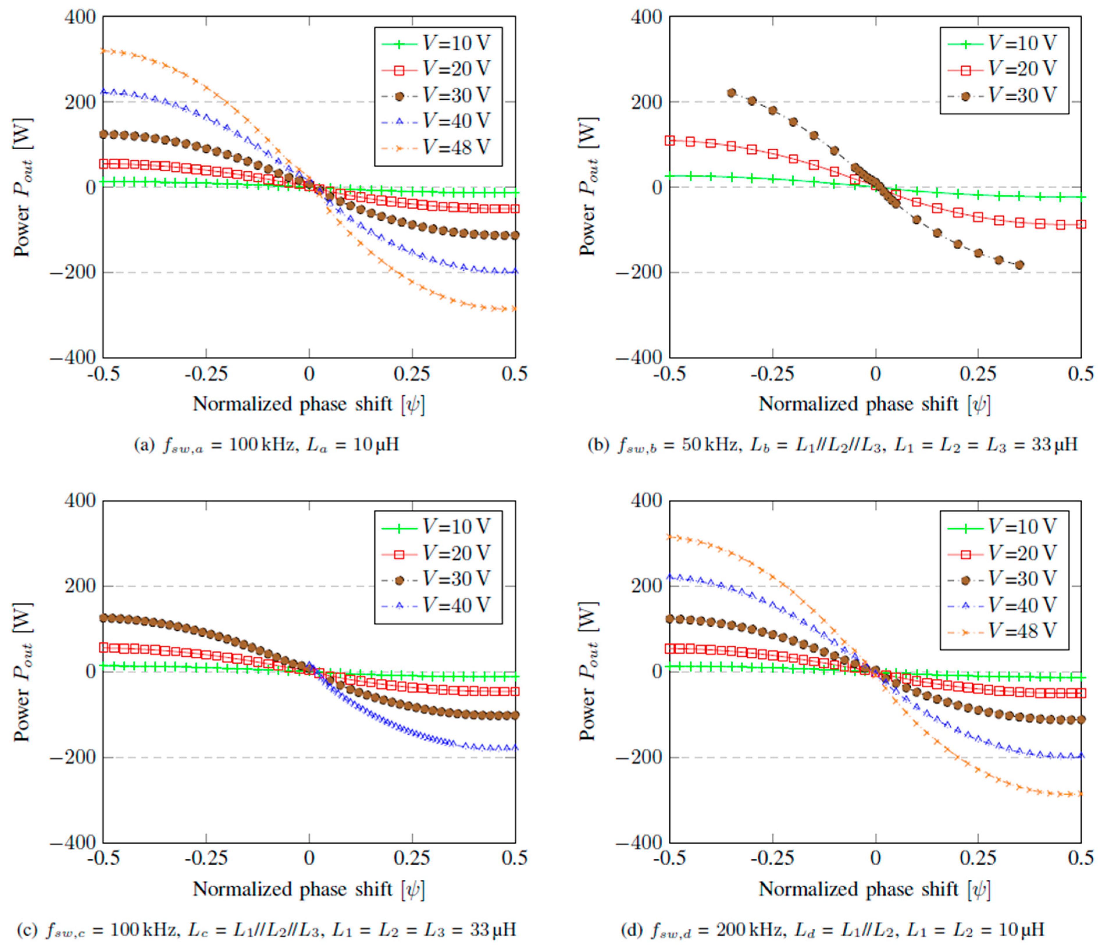
Figure 8.
Efficiency characterization at different voltages, frequencies, and inductance values, V = Vin = Vout.
Figure 8.
Efficiency characterization at different voltages, frequencies, and inductance values, V = Vin = Vout.
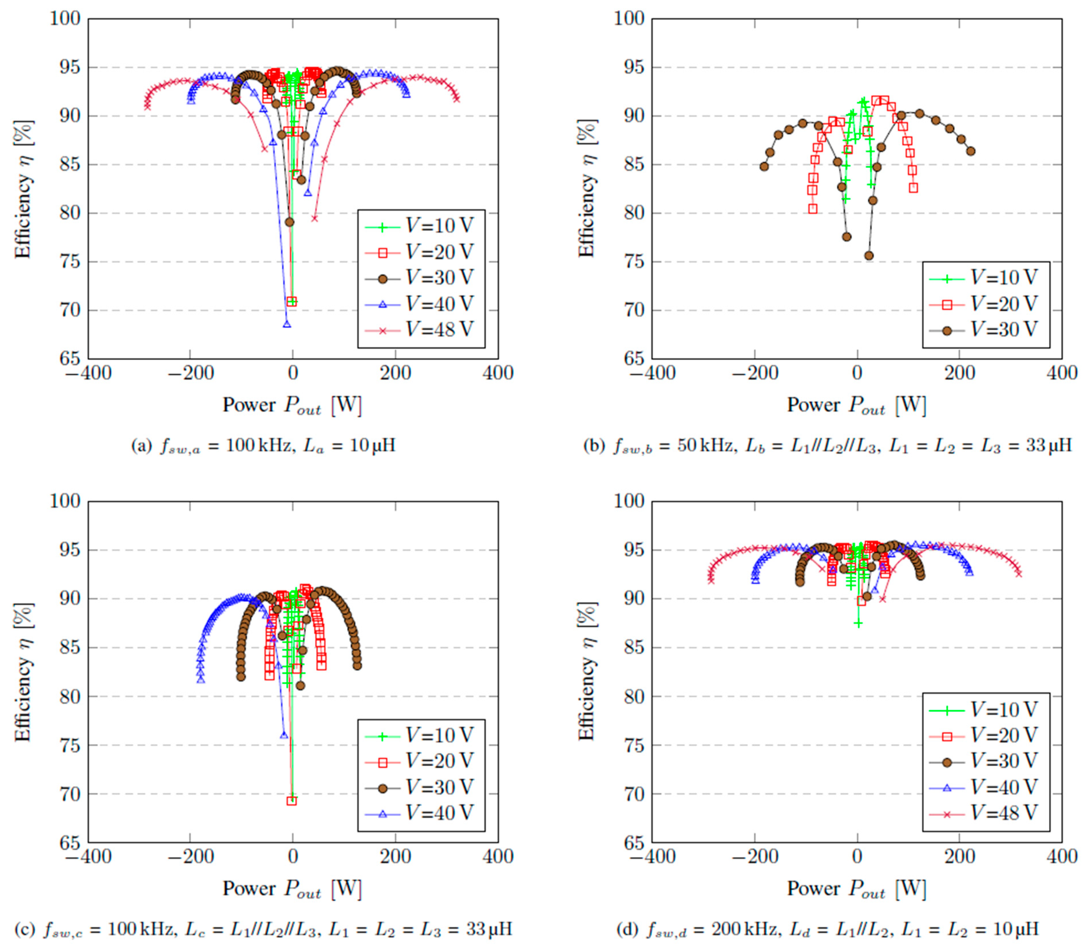
Figure 9.
Power points and maximum efficiency for different bus voltages (fsw = 100 kHz, L = 10 μH).
Figure 9.
Power points and maximum efficiency for different bus voltages (fsw = 100 kHz, L = 10 μH).
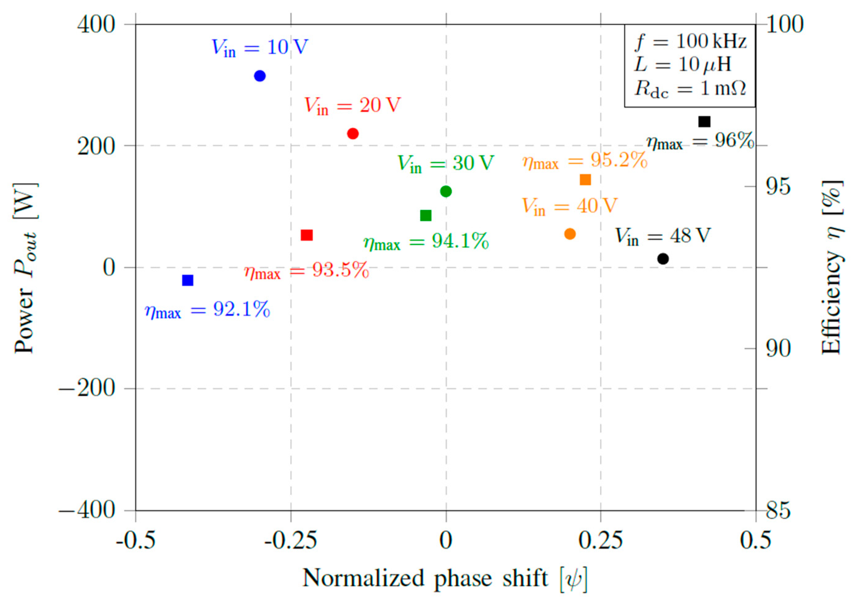
Figure 10.
Characterization of the different converter gains at M = 0.6, 1, and 1.4.
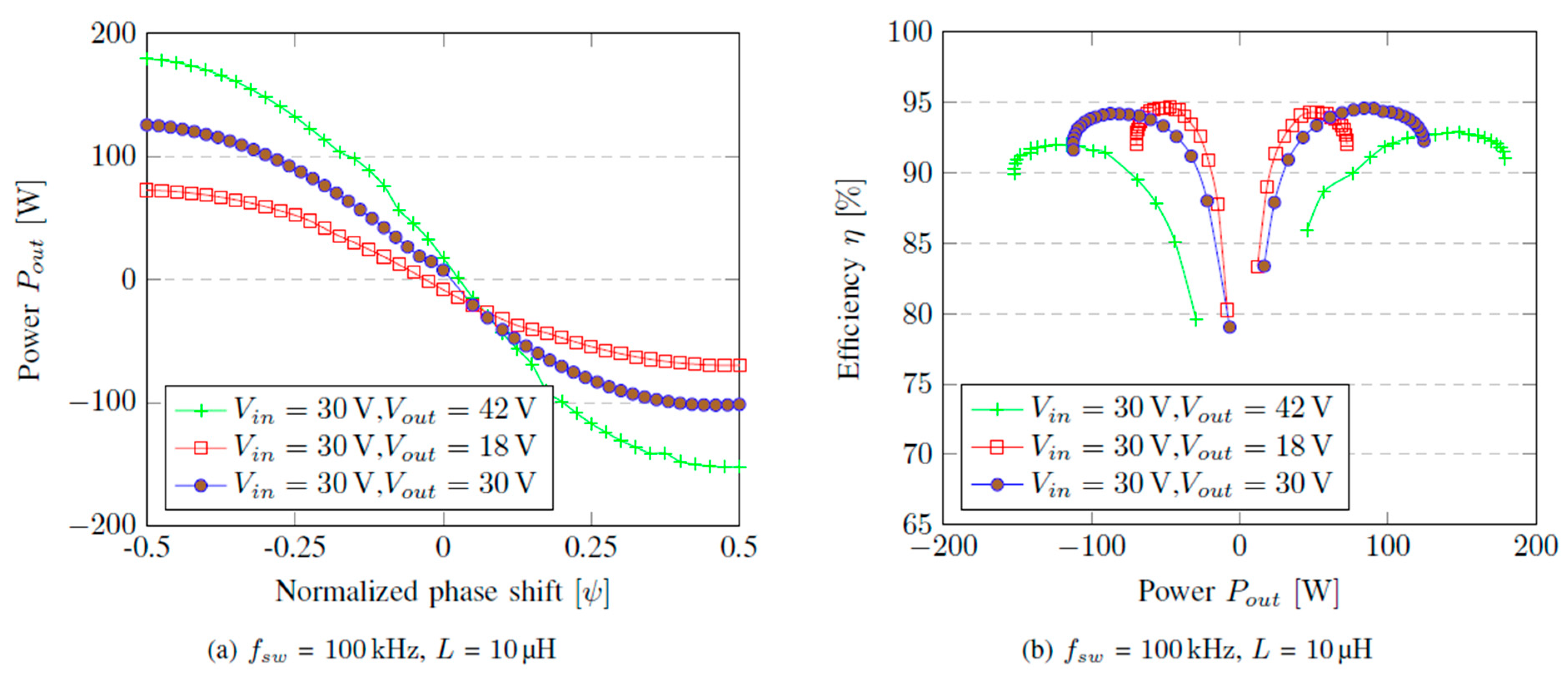
Figure 11.
HIL and experimental results, with L = 10 µH, fsw = 100 kHz, and different input and output voltages.
Figure 11.
HIL and experimental results, with L = 10 µH, fsw = 100 kHz, and different input and output voltages.
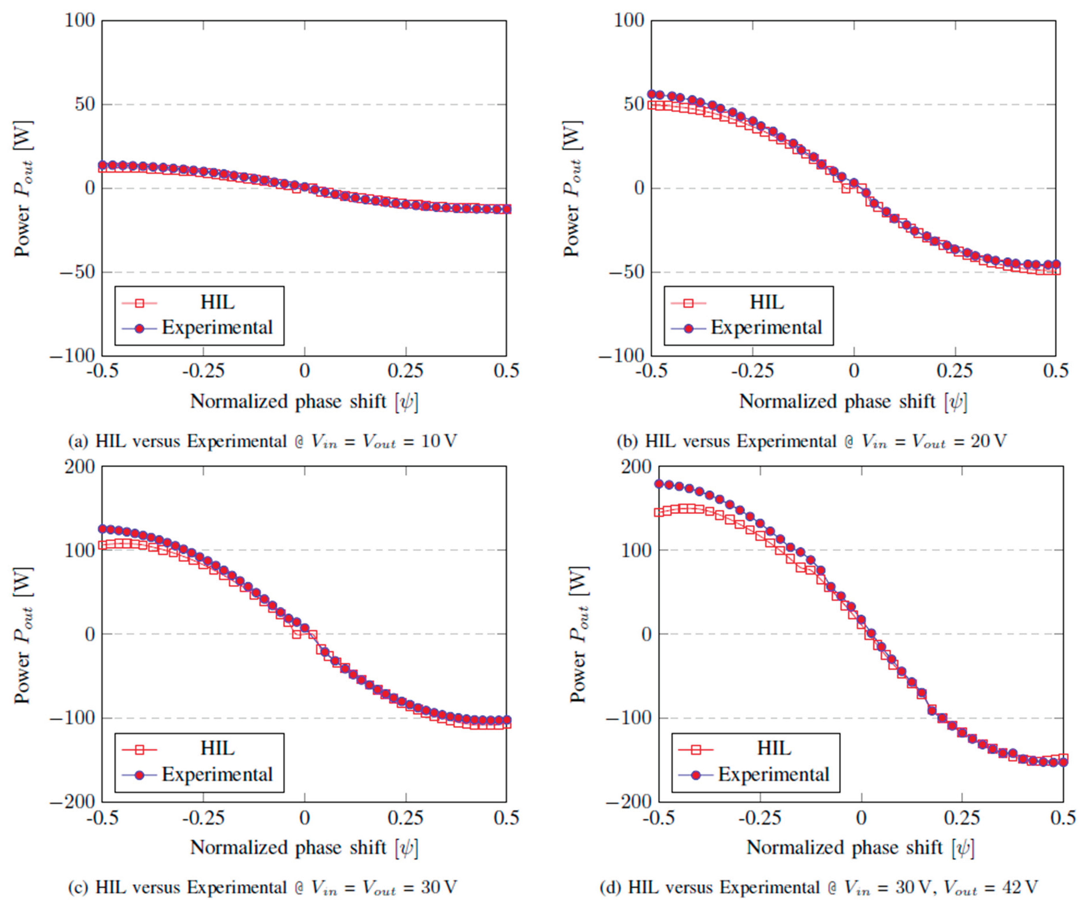

Table 1.
Specifications of the DAB converter of the early test.
| Parameters | Value |
|---|---|
| DC input voltage (Vin) | 10 V |
| DC output voltage (Vout) | 10 V |
| Transformer type | Coilcraft PL300-100L |
| Transformer turns ratio (1:n) | 1:1 |
| Series inductor L | 13 µH |
| HF filter capacitance C1, C2 | 58.6 µF, 58.6 µF |
| Primary-side and secondary-side MOSFETs | EPC23102 |
| Switching frequency | 100 kHz |
Disclaimer/Publisher’s Note: The statements, opinions and data contained in all publications are solely those of the individual author(s) and contributor(s) and not of MDPI and/or the editor(s). MDPI and/or the editor(s) disclaim responsibility for any injury to people or property resulting from any ideas, methods, instructions or products referred to in the content. |
© 2025 by the authors. Licensee MDPI, Basel, Switzerland. This article is an open access article distributed under the terms and conditions of the Creative Commons Attribution (CC BY) license (http://creativecommons.org/licenses/by/4.0/).
Copyright: This open access article is published under a Creative Commons CC BY 4.0 license, which permit the free download, distribution, and reuse, provided that the author and preprint are cited in any reuse.


