
Submitted:
28 November 2025
Posted:
01 December 2025
You are already at the latest version
Abstract
In the presented research, aluminum-doped zinc oxide (AZO) thin films were synthe-sized on high-power transmission lines using the RF magnetron sputtering process. The impact of deposition power (160 W to 280 W) and deposition pressure (2 Pa to 5 Pa), on the structural, surface, wettability and anti-icing properties of the films was thoroughly investigated. Key characteristics like material composition, wettability, an-ti-icing behavior, and average crystal size were analyzed. The optimization of wetta-bility and anti-icing performance was carried out using two-factor, four level design of the Taguchi method. Considerable variation in water contact angle from 92.3° to 123.6°, has been observed suggesting an enhancement in hydrophobic nature with op-timized condition. Anti-icing tests demonstrated that the coated surface delayed ice accumulation by approximately 4.56 times compared to the uncoated surface. X-ray diffraction (XRD) analysis was carried out to confirm notable changes in the intensity of the (002) peak along the c-axis, directly correlating with grain size modification. The change in surface roughness was studied using AFM and results were compared to es-tablish relation between surface roughness and average grain size. Overall, the find-ings highlight the critical role of deposition parameters and their interactions in modi-fying the surface and structural properties of AZO thin films, which demonstrates their potential application for improving the anti-icing performance of transmission lines.
Keywords:
thin film coating
; AZO thin film
; anti-icing property
; Taguchi
1. Introduction
The requirement of advance materials are increasing with each passing day. More advance materials with wide range of application are becoming heart of any industry. The development of these advance materials can be done by several methods, one of which is thin film coating. Thin films are useful for improving surface properties of any material. Various surface properties such as wettability, anti-icing, frictional property, surface roughness etc. can be controlled using nanoparticles.
Recent variations in global atmospheric circulation, including the displacement of polar air masses and fluctuations in the jet stream, have introduced extreme cold conditions in regions not typically exposed to such climates. Concurrently, the impacts of climate change are leading to snowfall in atypical geographic locations, thereby intensifying the problem of ice deposition across a wide range of engineering applications. In high-voltage power transmission systems, wind turbines, and aircraft, the accumulation of ice significantly compromises operational safety and efficiency. For example, in transmission lines, the additional load imposed by ice can overstress conductors and supporting towers, potentially resulting in mechanical failure. Conventional methods to resolve this issue which includes ice electrolysis system, pulse electro-thermal deicer, LC spiral rods, DC current method, etc, requires high operational costs, energy consumption, and the need for continuous supervision. Here considering that ice accumulation is fundamentally related with surface–water interactions, modification in surface property using surface engineering provides a promising route to mitigate this challenge. Typically, the icing accumulation progresses through two successive stages, first one being the deposition of super cooled water droplets on a surface, followed by their solidification into ice under subfreezing conditions. There are many materials which provides hydrophobic surface and holds potential to develop a good anti-icing properties which can be justified by the lotus effect [9].
Transparent Conducting Oxides have become the buzz of the field in recent years. Many materials have been researched extensively with an aim to develop transparent and conductive coating [1]. One of the most known oxide is ITO also known as In2O3 : Sn is most used Transparent Conducting Oxides (TCO), however the availability of ITO material is matter of concern. It has been observed that Zinc Oxide also hold identical properties and since Zinc is easily available and can be designed effectively, ZnO can become an alternative to ITO. Here ZnO is an n-type semiconductor, doping with suitable anionic or cationic elements is essential to reduce its resistivity. Materials like aluminum, indium, gallium, copper, cadmium etc [2]. can be used as dopant which will increase the free electrons into the semiconductor material’s crystal lattice and these electrons will become majority of charge carriers, ultimately increasing the conductivity of the semiconductor. Aluminum is one of the well-researched dopant for this application. Various methods like pulsed deposition method [3], chemical vapor deposition [4], atomic layer deposition [5], sputtering process [6] and even sol-gel [7] method can be used to develop such Aluminum doped – ZnO coating [8].
A limited body of literature is available on the wettability characteristics of aluminum-doped zinc oxide (AZO) thin films and their correlation with anti-icing behavior, particularly when applied to curved surfaces. To address this gap, the present study conducts a detailed investigation aimed at understanding the material’s performance in such applications. Thin films of AZO were deposited on high-voltage power transmission wire substrates using the RF magnetron sputtering technique. The influence of deposition power and chamber pressure on key properties—including wettability, anti-icing behavior, surface morphology, and average crystal size—was systematically examined.
2. Materials and Methods
For optimization, Taguchi has been implemented for identification of impact of power and pressure on wettability and anti-icing property. A two factor four level designed is implemented using orthogonal table of Taguchi design. For implementation of SN ratio, “HB” characteristic also known as “Higher is better” is implemented, Equation for the same is presented in Equation (1).
The Higher is Better (HB) characteristic:
Where,
n = number of observation
y = observation data
i = number of experiment which in this case is 16.
Orthogonal table for the experiment is shown in Table 1 with information regarding various factors and levels.
For deposition process magnetron sputtering process is used and deposition of parameters are shown in Table 2. Substrates are cleaned using acetone. And pre-sputtered for 10 mins in order to remove all the contaminants from the surface. For the purpose of material and chemical composition identification of deposited thin films, Cu-K radiation equipped X-ray Diffractometer (Bruker D2 phaser) with wavelength of 1.54 is used. For calculation of average grain size Scherrer formula shown in Equation (2) is used. Surface morphology of the thin film is analyzed using the AFM (Bruker Multimode Nanoscope-IV) and for study of topography of thin film Scanning Electron Microscopy is utilized. The study of wettability was carried out using a goniometer (Rame Hart 290). The identification of effect of Aluminum doped Zinc Oxide thin film on anti-icing property of surface is done using a customized Peltier platform developed using P-N junction, ice was kept on the side of heat sink in order to obtain low temperature.
3. Results
The identification of chemical composition and existence of aluminum doped zinc oxide thin film on surface was done using X-Ray Diffractometer. Thin films deposited with deposition power of 160W, 200W, 240W and 280W and deposition pressure with 2Pa, 3Pa, 4Pa, and 5Pa were studied using XRD. The change in peak intensity varies with change in each parameter for (002) peak and is shown in Figure 1. The observations indicate that an increase in deposition power results in a corresponding enhancement of peak intensity, which can be observed by the illustrated Figure 1 more over with increase in deposition pressure the intensity of peak decreases as illustrated in each individual graph shown Figure 1. The same results has been observed by N Patel and K Chauhan [10] for Al-ZnO thin film in their research which shows that with increase in deposition pressure the peak intensity decreases and with increase in power the high intensity peak with better crystallite is obtained. Yu G., Liu Y. et.al. [11] carried out a research in which they observed that peak intensity is directly in proportion with deposition power.
The average grain size for each sample was calculated using the Scherrer equation, as presented in Equation (2). This parameter was subsequently analyzed to understand the effect of deposition power and deposition pressure on the structural evolution of the thin films, Taguchi optimization was employed. Figure 2 illustrates the main effects plot for the means of grain size with respect to deposition power and deposition pressure. The results indicate that grain size increases with increase in deposition power. This behavior can be because of the enhanced energy of sputtered atoms at higher power levels, which improves their surface mobility and promotes the growth of larger crystallites. Conversely, an increase in deposition pressure leads to a reduction in grain size. This results can be justified by the higher probability of atomic collisions at higher pressures, which reduces the kinetic energy of sputtered atoms, which ultimately obstructs crystallite growth and resulting in smaller grain sizes. Similar findings have been reported by Brassard et al., who observed an increase in grain size with increasing deposition power [12,13,14,15].
A considerable variation in grain size was observed, with the average grain size ranging from 22.42 nm to 31.85 nm which is approximately 42.06% higher than the least favorable deposition condition, as presented in Figure 3. Similar trends were reported by Qian Shi et al. [17] in 2014, where it was demonstrated that crystallite size displays a direct dependence on deposition power and an inverse dependence on deposition pressure. Here Table 3 can be used to understand the change in average grain size.
The study of surface morphology was conducted from the images obtained from the SEM as shown in Figure 4. The examination of surface morphology at a deposition pressure of 5 Pa with different deposition power shows relative dependency of grain formation on deposition power. Specifically, it was observed that with increase in deposition power the crystal size also increases. This behavior can be attributed to the enhanced energy of sputtered particles at higher power levels, which promotes improved adatom mobility on the substrate surface, thereby facilitating the formation of larger crystalline structures [18]. This observation provides a supporting proof to our previous analysis obtained from the XRD data. When the deposition power was increased, the energy obtained by the sputtering atom also increased, leading to more freely movement of atoms on the surface of thin film, and eventually providing a better crystal structure to the thin film.
To study the topography of deposited thin film Atomic Force Microscopy is implemented. Figure 5(a) represents the Main Effects Plot for Means of surface roughness and its relation with deposition pressure and deposition power. The results distinctly indicate that an increase in deposition power leads to a corresponding rise in surface roughness. This phenomenon can be explained by the observed variation in grain size, wherein higher deposition power enhances the energy of incident particles, promoting greater adsorbed atom mobility and facilitating the growth of larger crystallites. The enlargement of these crystallites contributes to increasing the overall surface roughness. Such a correlation between deposition power, grain size, and surface roughness highlights the strong interdependence between deposition parameters and the morphological characteristics of the thin films. While if we consider the impact of deposition pressure which reduces the surface roughness and provides smoother surface. M. Marikkannan et al. reported similar findings, demonstrating that an increase in deposition power leads to higher surface roughness. Furthermore, their study highlighted that variations in surface roughness significantly influence the surface quality, wherein optimized conditions yield comparatively smoother surfaces [19]. This phenomenon reveals the fact that when the bombardment energy was increased upto certain level the surface roughness also increased along with the crystal size and the smoothness of the surface decreased subsequently. While Figure 5(b) represents the main effects plot for SN ratio. Results obtained from SN ratio showed that surface roughness is largely impacted by deposition power while if we consider deposition power, its effect on surface roughness is considerably less compared to power.
Here Figure 6 represents images obtained from AFM. The variation in surface roughness with deposition power and deposition pressure is presented in Figure 7. Which represents a significant variation in surface roughness from 290 nm to 766 nm which is 164.13% higher than the least favorable deposition parameters.
For optimization study of wettability, response table for Signal to Noise ratios is shown in Table 4. The results conclude variation in wettability from 92.3o to 123.6o, which is 33.91% higher than the least favorable deposition parameter and 62.63% higher than the uncoated surface. The delta value of Power is 2.07 and of Pressure it is 0.42, which clearly states the impact of each parameter. Change in deposition power impacts wettability significantly higher than pressure. The same conclusion is observed for surface roughness as well. The relation between surface roughness and wettability can be explained by Cassie – Baxter model, which states that with increase in surface roughness the wettability also increases, which leads to better hydrophobic nature [20]. The relationship between surface roughness and wettability is illustrated in Figure 8, which demonstrates a consistent pattern, indicating that variations in surface roughness are directly reflected in corresponding changes in wettability [21].
For the study of anti-icing property, a device known as Peltier platform was used to identify the ice accumulation on the surface. In this study the delay in ice accumulation was studied as a function of deposition power and deposition pressure. In order to identify the delay in ice accumulation the heat sink of Peltier platform was placed on surface of ice with temperature of -15oC. For the deposition power of 160W, 200W, 240W and 280W and pressure is varied from 2Pa to 5Pa, time delay of 4.556x is obtained when compared with uncoated conductor as shown in Figure 9.
The key factors affecting the ice accumulation is surface energy and the water contact angle. When low surface energy with high contact angle is obtained, which leads to significant delay in ice accumulation. The same results were observed and validated by S. Noormohammed and D. Sarkar [22], who provided the observation that when the contact angle increases and surface energy decreases the ice accumulation can be delayed significantly with decrease in ice adhesion to the surface [23].
5. Conclusions
The deposition of Al-doped zinc oxide thin film was studied with a function of deposition power and deposition pressure. Here in this study the XRD results showed that with at low deposition power and higher deposition pressure the peak intensity of (002) is comparatively week however with increase in deposition power and decrease in deposition pressure higher peak intensity with better crystal structure is obtained. Consideration of average grain size with variation in deposition parameter led to a conclusion that when high pressure is provided to sputtered atom, a better crystallite is generated leading to increase in average grain size, at the same time if we study the effect of high deposition pressure, it leads to a conclusion that with increase in deposition pressure, the collision probability of free atoms increased, leading to smaller grain size with smoother surface. A variation from 22.42nm to 31.85nm is observed in grain size, here a significant variation of 42.06% is observed from most favorable deposition parameter to least deposition parameter. The roughness of surface also increased with increase in deposition power and decrease in deposition pressure, a direct relation has been observed between grain size and surface roughness. Here in the presented research the surface roughness increases from 290 nm to 766 nm which is significant increment of around 164.13%. A maximum water contact angle of around 123.6o was obtained at the deposition power of 280W and deposition pressure of 2Pa and comparison showed that it is approximately 33.91% higher than least favorable condition and 62.63% higher than the uncoated surface. Due to change in value of contact angle the time for ice accumulation was delayed by 4.556 fold while comparing with uncoated substrate which is a significant improvement of 455.6%.
References
- B. Szyszka et al., “Recent developments in the fi eld of transparent conductive oxide fi lms for spectral selective coatings , electronics and photovoltaics,” vol. 12, pp. 2–11, 2012. [CrossRef]
- S. T. Khlayboonme and W. Thowladda, “Impact of Al-doping on structural , electrical , and optical properties of sol-gel dip coated ZnO : Al thin films Impact of Al-doping on structural , electrical , and optical properties of sol-gel dip coated ZnO : Al thin fi lms.”.
- G. Socol et al., “substrates,” Appl. Surf. Sci., no. November, 2012. [CrossRef]
- D. Kim, I. Yun, and H. Kim, “Fabrication of rough Al doped ZnO films deposited by low pressure chemical vapor deposition for high efficiency thin film solar cells,” Curr. Appl. Phys., vol. 10, no. 3, pp. S459–S462, 2010. [CrossRef]
- A. Di, M. Cantarella, G. Nicotra, and V. Privitera, “Applied Catalysis B : Environmental Low temperature atomic layer deposition of ZnO : Applications in photocatalysis,” "Applied Catal. B, Environ., vol. 196, pp. 68–76, 2016. [CrossRef]
- S. C. Target, “Sprayed Composite Target,” 2021.
- K. Daoudi, B. Canut, M. G. Blanchin, C. S. Sandu, V. S. Teodorescu, and J. A. Roger, “Densification of In 2 O 3 : Sn multilayered films elaborated by the dip-coating sol – gel route,” vol. 445, no. 03, pp. 20–25, 2003. 2003; 25. [CrossRef]
- D. Mendil et al., “US,” 2019.
- B. Stieberova, M. Zilka, M. Ticha, F. Freiberg, and E. Lester, “Application of ZnO nanoparticles in Self-Cleaning Coating on a Metal Panel : An Assessment of Environmental Benefits.”.
- N. P. Patel and K. V Chauhan, “Effect of sputtering power and substrate temperature on structural , optical , wettability and anti-icing characteristics of aluminium doped zinc oxide Effect of sputtering power and substrate temperature on structural , optical , wettability and anti-icing characteristics of aluminium doped zinc oxide.”.
- G. Yu, Y. Liu, D. Hong, D. Li, and J. Zang, “Influence of Sputtering Power and Substrate Temperature on properties of Al 2 O 3 -doped ZnO Films,” vol. 559, pp. 1945–1949, 2012. [CrossRef]
- Brassard, D. K. Sarkar, and J. Perron, “Applied Surface Science Studies of drag on the nanocomposite superhydrophobic surfaces,” Appl. Surf. Sci., vol. 324, pp. 525–531, 2015. [CrossRef]
- T. Guo et al., “Superlattices and Microstructures Optimization of oxygen and pressure of ZnO : Al films deposited on PMMA substrates by facing target sputtering,” Superlattices Microstruct., vol. 64, pp. 552–562, 2013. [CrossRef]
- A. B. Gurav et al., “Superhydrophobic surface decorated with vertical ZnO nanorods modi fi ed by stearic acid,” Ceram. Int., vol. 40, no. 5, pp. 7151–7160, 2014. [CrossRef]
- D. Kim et al., “Materials Science in Semiconductor Processing Effects of oxygen concentration on the properties of Al-doped ZnO transparent conductive films deposited by pulsed DC magnetron sputtering,” Mater. Sci. Semicond. Process., vol. 16, no. 3, pp. 997–1001, 2013. [CrossRef]
- S. Mustapha, M. M. Ndamitso, A. S. Abdulkareem, and J. O. Tijani, “Comparative study of crystallite size using Williamson-Hall and Debye- Comparative study of crystallite size using Williamson-Hall and Debye-Scherrer plots for ZnO nanoparticles,” 2019.
- Q. Shi, K. Zhou, M. Dai, S. Lin, H. Hou, and C. Wei, “Growth of high-quality Ga – F codoped ZnO thin fi lms by mid-frequency sputtering,” Ceram. Int., vol. 40, no. 1, pp. 211–216, 2014. [CrossRef]
- P. Zhang, R. Y. Hong, Q. Chen, and W. G. Feng, “On the electrical conductivity and photocatalytic activity of aluminum-doped zinc oxide On the electrical conductivity and photocatalytic activity of aluminum-doped zinc oxide,” Powder Technol., vol. 253, no. April, pp. 360–367, 2022. 2022. [CrossRef]
- M. Marikkannan, A. Dinesh, J. Mayandi, V. Vishnukanthan, and J. M. Pearce, “Properties of Al-Doped Zinc Oxide and In-Doped Zinc Oxide Bilayer,” Mater. Lett., 2018. 2018. [CrossRef]
- J. Lee, B. He, and N. A. Patankar, “A roughness-based wettability switching membrane device for hydrophobic surfaces,” vol. 591. [CrossRef]
- S. K. Rawal, A. Kumar, V. Chawla, R. Jayaganthan, and R. Chandra, “Structural , optical and hydrophobic properties of sputter deposited zirconium oxynitride films,” Mater. Sci. Eng. B, vol. 172, no. 3, pp. 259–266, 2010. [CrossRef]
- S. Noormohammed, “Nanostructured Titanium Dioxide Coating on Aluminum Alloy for Icephobic Applications,” 2021.
- Y. Wu et al., “An extremely chemical and mechanically durable siloxane bearing copolymer coating with self-crosslinkable and anti-icing properties,” Compos. Part B, vol. 195, no. March, p. 108031, 2020. [CrossRef]
Figure 1.
X-ray diffraction spectra for Al:ZnO.
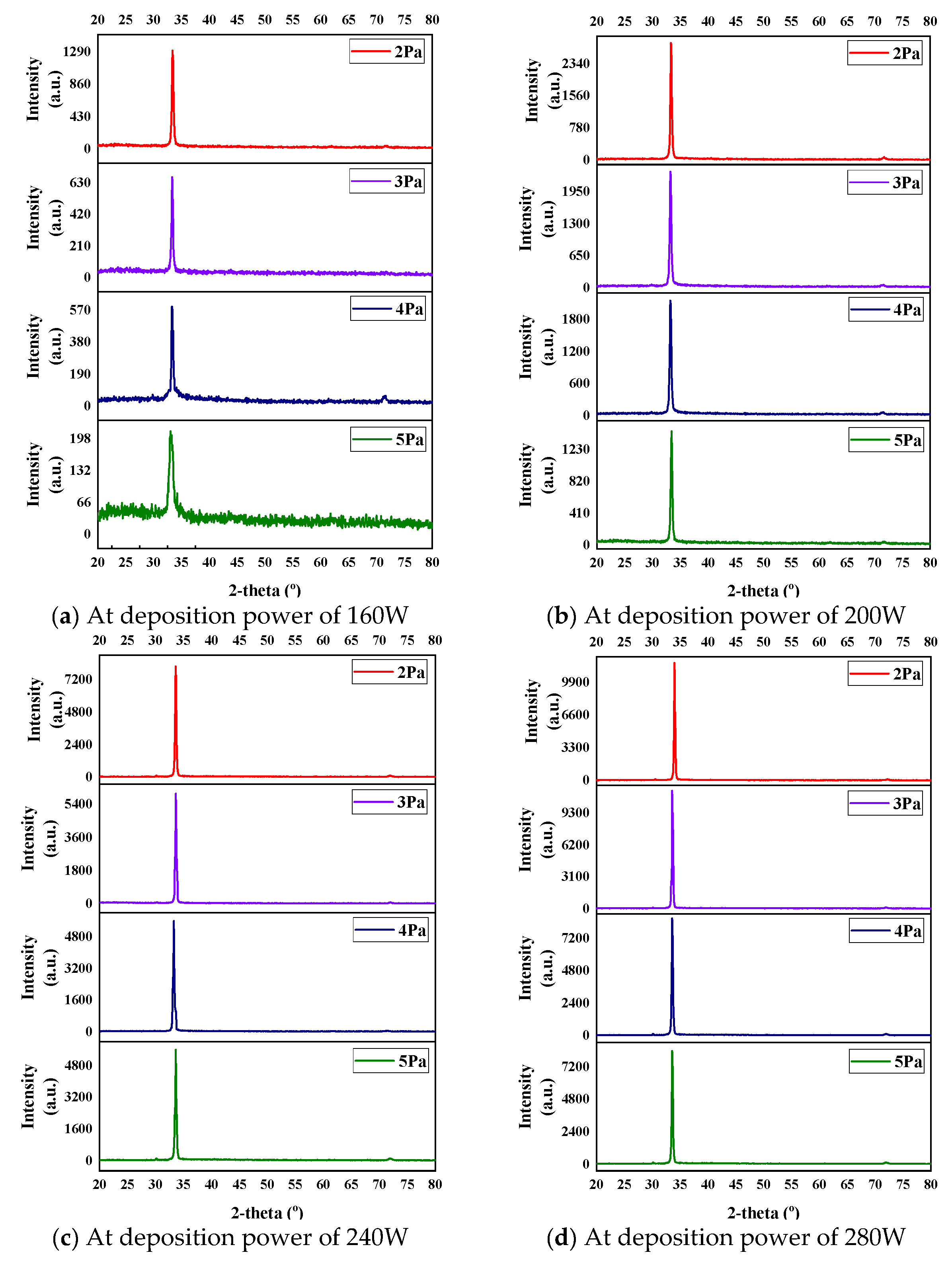
Figure 2.
Main Effects Plot for Means: GRAIN SIZE versus POWER and PRESSURE.
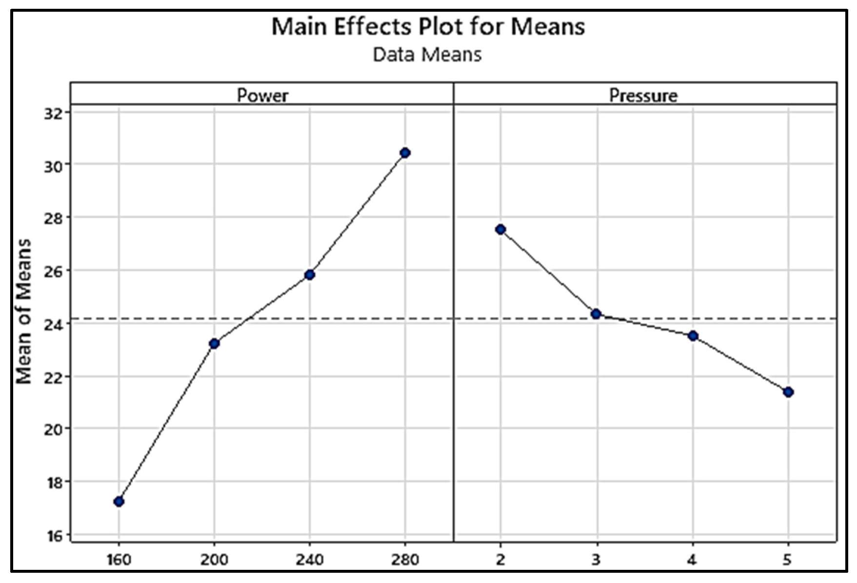
Figure 3.
Change in average grain size with respect to sputtering power and deposition pressure for aluminum doped zinc oxide thin film.
Figure 3.
Change in average grain size with respect to sputtering power and deposition pressure for aluminum doped zinc oxide thin film.
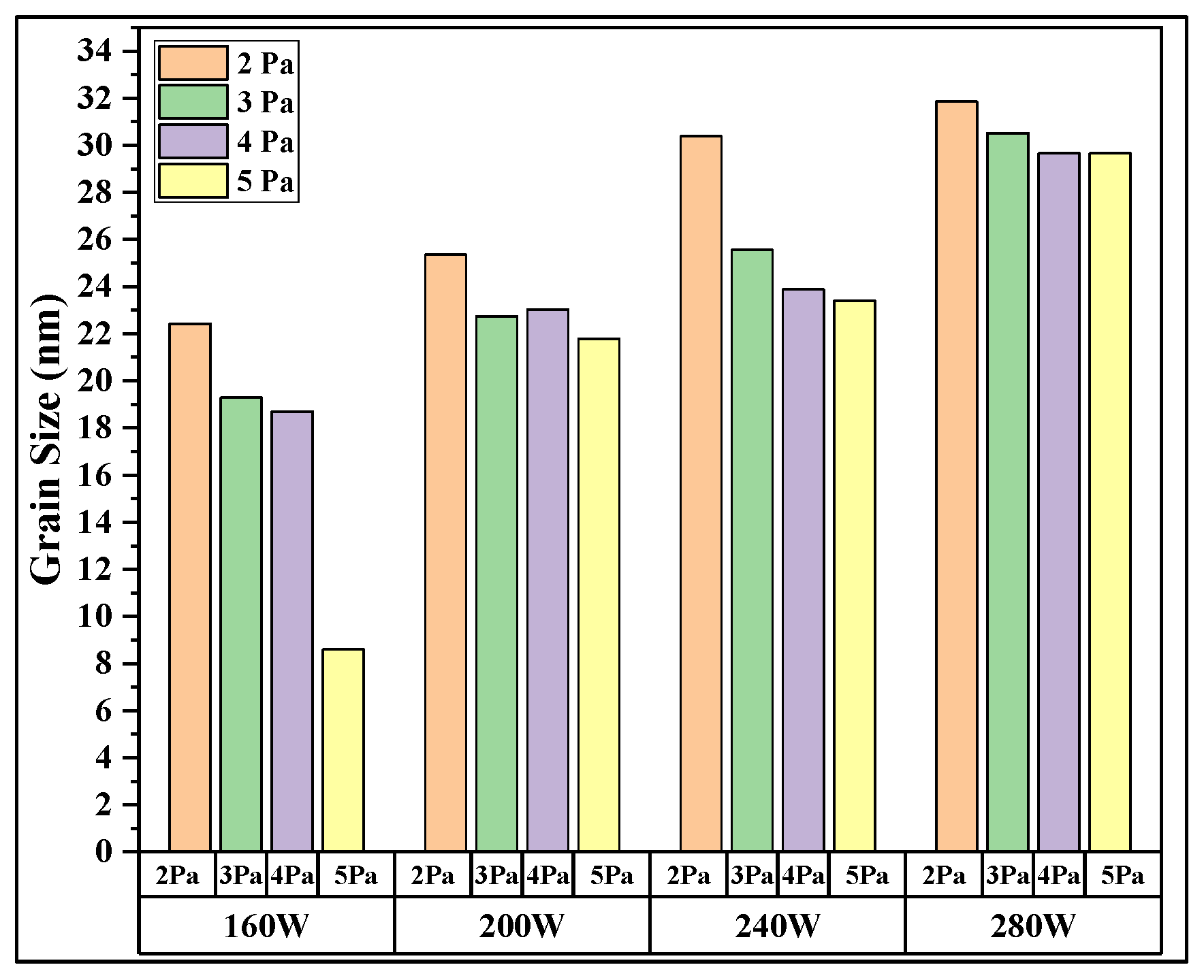
Figure 4.
Image obtained from Scanning Electron Microscope for (a) 160W, (b) 200W, (c) 240W and (d) 280W for Al:ZnO thin film at 5 Pa.
Figure 4.
Image obtained from Scanning Electron Microscope for (a) 160W, (b) 200W, (c) 240W and (d) 280W for Al:ZnO thin film at 5 Pa.
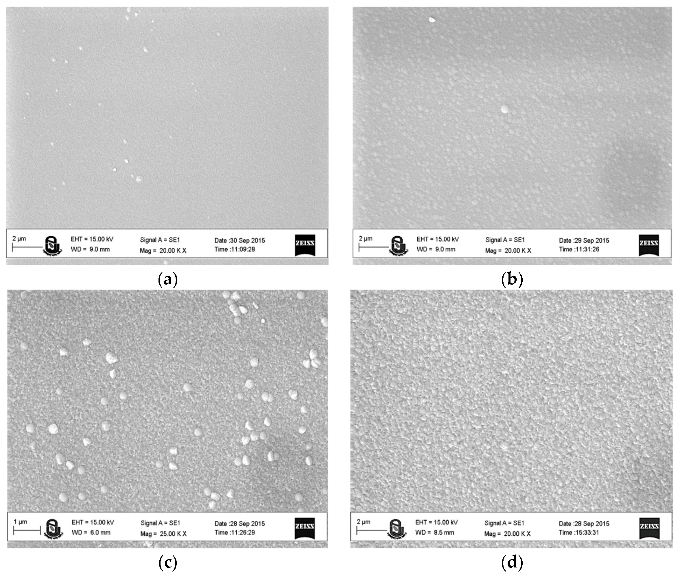
Figure 5.
(a) Main Effects plot for means for surface roughness VS deposition power and deposition pressure. (b) Main Effects plot for SN ratio for surface roughness VS deposition power and deposition pressure.
Figure 5.
(a) Main Effects plot for means for surface roughness VS deposition power and deposition pressure. (b) Main Effects plot for SN ratio for surface roughness VS deposition power and deposition pressure.
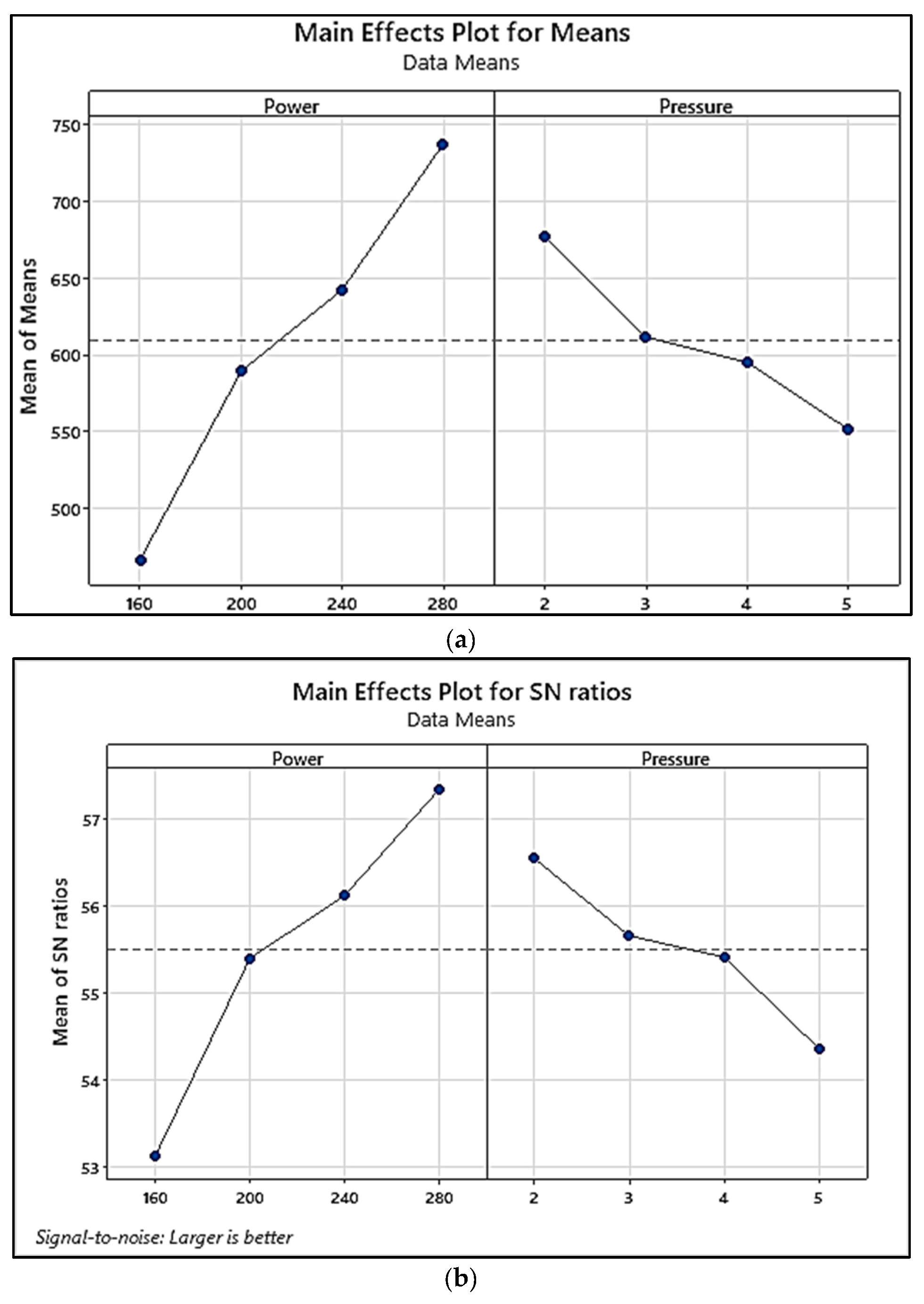
Figure 6.
AFM output of as deposited film.
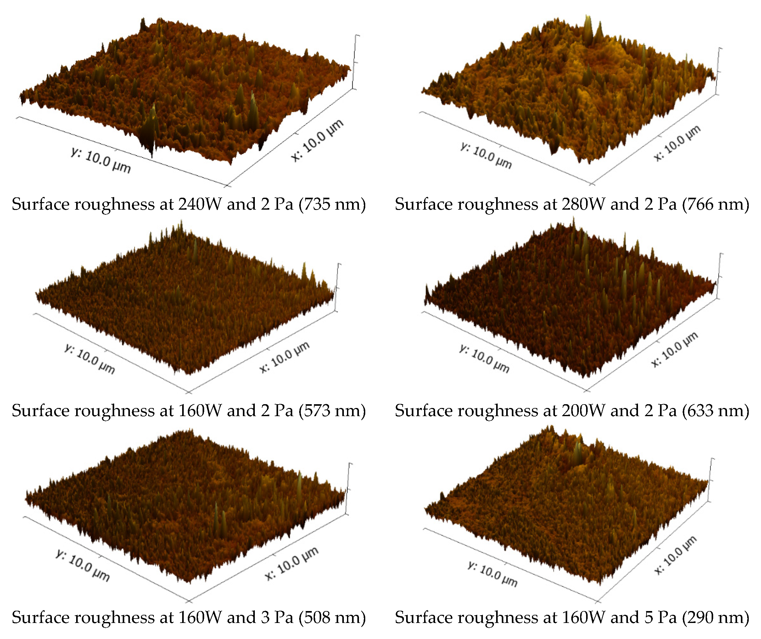
Figure 7.
Variation in surface roughness of Al-doped ZnO thin film for different RF deposition power and pressure.
Figure 7.
Variation in surface roughness of Al-doped ZnO thin film for different RF deposition power and pressure.
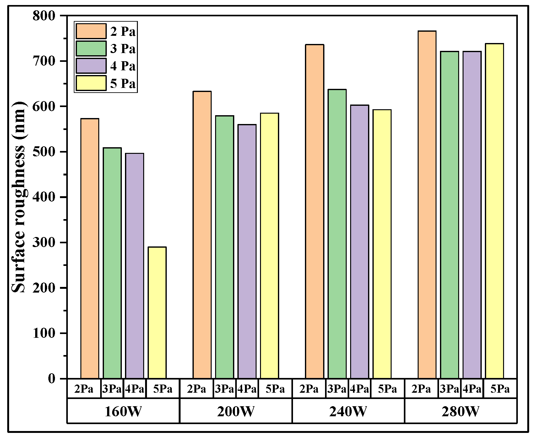
Figure 8.
Effect of deposition power and deposition pressure on surface roughness and wettability of aluminum doped zinc oxide thin film.
Figure 8.
Effect of deposition power and deposition pressure on surface roughness and wettability of aluminum doped zinc oxide thin film.
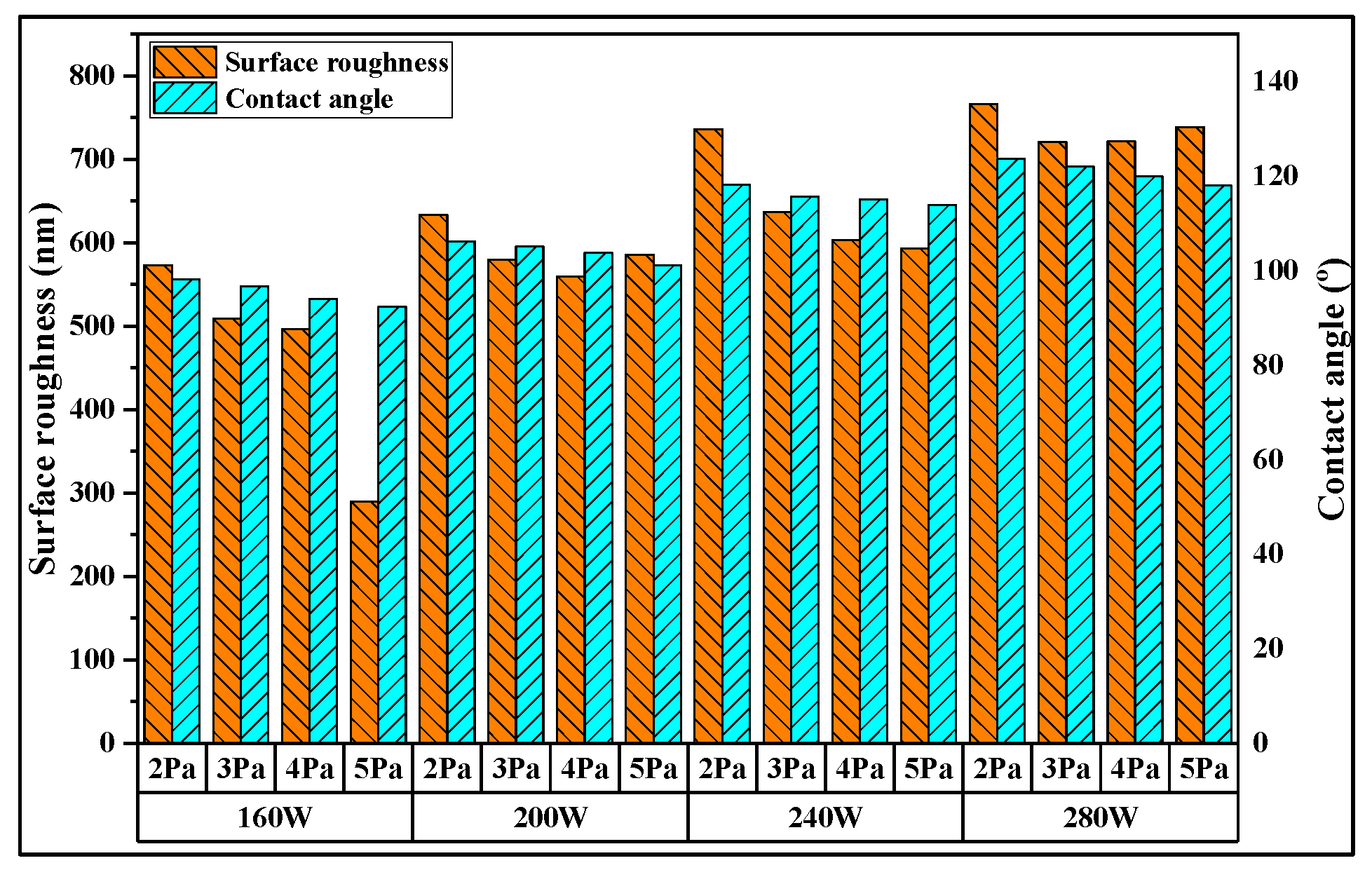
Figure 9.
Effect of deposition power and deposition pressure on delay in ice accumulation of aluminum doped zinc oxide thin film.
Figure 9.
Effect of deposition power and deposition pressure on delay in ice accumulation of aluminum doped zinc oxide thin film.
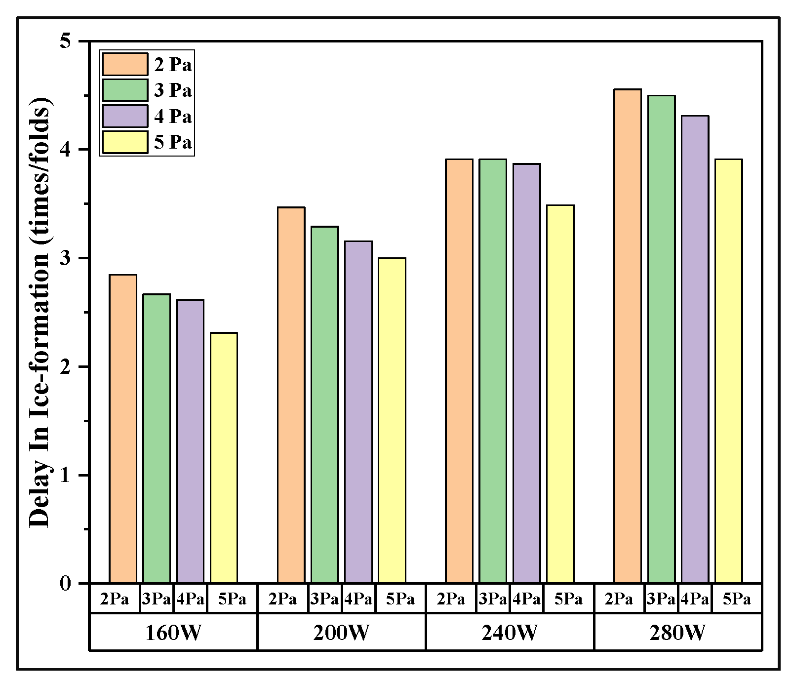

Table 1.
Deposition parameters for Development of Al doped Zinc Oxide thin film.
| Substrate :- | High Power transmission line (Panther conductor), Corning glass | ||||||
| Target material :- | AZO (99.999% purity) | ||||||
| Base Pressure :- | 1 * 10-3 Pa | ||||||
| Substrate to target distance :- | 50 mm | ||||||
| Substrate temperature :- | Room temperature | ||||||
| Deposition time :- | 30 min | ||||||
| Sputtering gas :- | Ar ( with flow rate of 10 SCCM) | ||||||
|
Target gas symbol |
Control factors | Level 1 | Level 2 | Level 3 | Level 4 | ||
| A | Deposition Power (W) | 160 | 200 | 240 | 280 | ||
| B | Deposition Pressure (Pa) | 2 | 3 | 4 | 5 | ||
Table 2.
Deposition parameter for synthesis of Al doped zinc oxide thin film using RF sputtering process.
Table 2.
Deposition parameter for synthesis of Al doped zinc oxide thin film using RF sputtering process.
| Design Summary :- | ||||||||||
| Taguchi Array :- L16 (4^2) | ||||||||||
| Factors :- 2 | ||||||||||
| Runes :- 16 | ||||||||||
| Columns of L16 (4^2) array : 1 2 | ||||||||||
| Deposition temperature :- Room temperature | ||||||||||
| Deposition time :- 30 min | ||||||||||
| Sputtering gas :- Ar with gas flowrate of 10SCCM | ||||||||||
| Sample name | Encoded factors | Decoded factors | ||||||||
| A (W) | B (Pa) | Power (W) | Pressure (Pa) | |||||||
| Sample 1 | 1 | 1 | 160 | 2 | ||||||
| Sample 2 | 1 | 2 | 160 | 3 | ||||||
| Sample 3 | 1 | 3 | 160 | 4 | ||||||
| Sample 4 | 1 | 4 | 160 | 5 | ||||||
| Sample 5 | 2 | 1 | 200 | 2 | ||||||
| Sample 6 | 2 | 2 | 200 | 3 | ||||||
| Sample 7 | 2 | 3 | 200 | 4 | ||||||
| Sample 8 | 2 | 4 | 200 | 5 | ||||||
| Sample 9 | 3 | 1 | 240 | 2 | ||||||
| Sample 10 | 3 | 2 | 240 | 3 | ||||||
| Sample 11 | 3 | 3 | 240 | 4 | ||||||
| Sample 12 | 3 | 4 | 240 | 5 | ||||||
| Sample 13 | 4 | 1 | 280 | 2 | ||||||
| Sample 14 | 4 | 2 | 280 | 3 | ||||||
| Sample 15 | 4 | 3 | 280 | 4 | ||||||
| Sample 16 | 4 | 4 | 280 | 5 | ||||||
Table 3.
Change in average grain size derived suing Scherrer formula.
| Sample name | Decoded factors | Results | ||
| Power (W) | Pressure (Pa) | Average grain size (nm) | SN ratio | |
| Sample 1 | 160 | 2 | 22.4289 | 27.0162 |
| Sample 2 | 160 | 3 | 19.2921 | 25.7076 |
| Sample 3 | 160 | 4 | 18.699 | 25.4364 |
| Sample 4 | 160 | 5 | 8.6039 | 18.694 |
| Sample 5 | 200 | 2 | 25.3631 | 28.084 |
| Sample 6 | 200 | 3 | 22.7393 | 27.1356 |
| Sample 7 | 200 | 4 | 21.7846 | 26.763 |
| Sample 8 | 200 | 5 | 23.0297 | 27.2458 |
| Sample 9 | 240 | 2 | 30.3812 | 29.6521 |
| Sample 10 | 240 | 3 | 25.5565 | 28.15 |
| Sample 11 | 240 | 4 | 23.8829 | 27.5617 |
| Sample 12 | 240 | 5 | 23.394 | 27.3821 |
| Sample 13 | 280 | 2 | 31.8523 | 30.0628 |
| Sample 14 | 280 | 3 | 29.667 | 29.4455 |
| Sample 15 | 280 | 4 | 29.6698 | 29.4463 |
| Sample 16 | 280 | 5 | 30.5163 | 29.6906 |
Table 4.
Relation of wettability with deposition power and pressure with response table of Signal to Noise Ratios.
Table 4.
Relation of wettability with deposition power and pressure with response table of Signal to Noise Ratios.
| Deposition temperature :- Room temperature | |||||||||
| Deposition time :- 30 min | |||||||||
| Sputtering gas :- Ar with gas flowrate of 10SCCM | |||||||||
| Sample name | Factors | Results | |||||||
| Power (W) | Pressure (Pa) | Contact angle (o) | SNR | ||||||
| Sample 1 | 160 | 2 | 98.2 | 39.84223 | |||||
| Sample 2 | 160 | 3 | 96.7 | 39.70853 | |||||
| Sample 3 | 160 | 4 | 94 | 39.46256 | |||||
| Sample 4 | 160 | 5 | 92.3 | 39.30403 | |||||
| Sample 5 | 200 | 2 | 106.2 | 40.52249 | |||||
| Sample 6 | 200 | 3 | 105.1 | 40.43205 | |||||
| Sample 7 | 200 | 4 | 103.7 | 40.31558 | |||||
| Sample 8 | 200 | 5 | 101.1 | 40.09502 | |||||
| Sample 9 | 240 | 2 | 118.2 | 41.45235 | |||||
| Sample 10 | 240 | 3 | 115.6 | 41.25916 | |||||
| Sample 11 | 240 | 4 | 115 | 41.21396 | |||||
| Sample 12 | 240 | 5 | 113.8 | 41.12285 | |||||
| Sample 13 | 280 | 2 | 123.6 | 41.84037 | |||||
| Sample 14 | 280 | 3 | 122 | 41.7272 | |||||
| Sample 15 | 280 | 4 | 120 | 41.58362 | |||||
| Sample 16 | 280 | 5 | 118 | 41.43764 | |||||
| Response table Signal to Noise ratio | |||||||||
| Larger is Better | |||||||||
| Level | Power | Pressure | |||||||
| 1 | 39.58 | 40.91 | |||||||
| 2 | 40.34 | 40.78 | |||||||
| 3 | 41.26 | 40.64 | |||||||
| 4 | 41.65 | 40.49 | |||||||
| Delta | 2.07 | 0.42 | |||||||
| Rank | 1 | 2 | |||||||
Disclaimer/Publisher’s Note: The statements, opinions and data contained in all publications are solely those of the individual author(s) and contributor(s) and not of MDPI and/or the editor(s). MDPI and/or the editor(s) disclaim responsibility for any injury to people or property resulting from any ideas, methods, instructions or products referred to in the content. |
© 2025 by the authors. Licensee MDPI, Basel, Switzerland. This article is an open access article distributed under the terms and conditions of the Creative Commons Attribution (CC BY) license (http://creativecommons.org/licenses/by/4.0/).
Copyright: This open access article is published under a Creative Commons CC BY 4.0 license, which permit the free download, distribution, and reuse, provided that the author and preprint are cited in any reuse.


