

Submitted:
27 October 2025
Posted:
28 October 2025
You are already at the latest version
Abstract
A compact 8–15 GHz Doherty power amplifier (DPA) is proposed and fabricated in 22-nm FD-SOI CMOS. The proposed DPA relies on quadrature-hybrid splitter and combiner to replace the bulky λ/4 impedance inverters at the input and the output of the conventional DPA enabling load modulation over a large fractional bandwidth (FBW=61%) with efficient and compact integration. The proposed DPA achieves a peak gain of 19.6 dB; ≥ 17 dB across 8–15 GHz, 18 dBm P1dB, 19.5 dBm Psat, and a peak PAE of 21% at 10 GHz, while sustaining 17% PAE at 6 dB back-off. The proposed DPA enables a modulation BW up to 200 MHz for a 256-QAM single carrier (SC) signal with a peak to average power ratio (PAPR) of 6 dB. Under this setting, the average output power (Pavg) is measured at 12.5 dBm with an RMS error vector magnitude (EVM) of −24.3 dB and an average PAE of 15%. Within the scope of CMOS power amplifiers in 22-nm FD-SOI, we found no published example that jointly demonstrates 8–15 GHz coverage and sustained PAE at 6 dB back-off using a quadrature hybrid.
Keywords:
Doherty power amplifier (DPA)
; X-band
; Ku-band
; CMOS
; 22-nm FD-SOI
; quadrature hybrid coupler
; impedance inverter
; millimeter-wave integrated circuits
1. Introduction
Next-generation microwave transmitters—including satellite payloads, phased arrays, and high-capacity backhaul—demand power amplifiers (PAs) that are both compact and efficient across wide frequency spans to enable low-cost, large-scale integration. Achieving these targets in nanoscale CMOS is challenging due to reduced supply voltages, device breakdown limits, and RF substrate losses that depress output power and power-added efficiency (PAE) [1].
In silicon technologies, substrate-induced loss and parasitics in passives and interconnects are first-order constraints on achievable efficiency and bandwidth. Silicon-on-insulator (SOI) platforms alleviate loss compared with bulk CMOS; however, aggressive scaling of the buried oxide and metal stack can reintroduce attenuation and phase error in on-chip lines and networks. For example, in 22-nm FD-SOI, on-chip transmission lines may incur on the order of 0.5 dB/mm loss around 10–12 GHz, with commensurate phase dispersion that penalizes Doherty load modulation if not co-optimized [2].
The Doherty power amplifier (DPA) is a leading architecture for high efficiency at output back-off, but classical quarter-wave () impedance inverters are area- and loss-prohibitive at X/Ku bands: even with slow-wave structures, sections are millimeters long and introduce multi-dB loss, eroding PAE and narrowing bandwidth [3,4].
To mitigate these limits, prior works explored alternative load-modulation networks and multi-input DPAs, trading off complexity, area, or broadband performance [5,6].
This work leverages a compact quadrature hybrid as a unifying element for both the input splitter and the output combiner, thereby realizing the load modulation for Doherty operation while simultaneously improving bandwidth and reducing footprint. The fabricated DPA in GlobalFoundries 22-nm FD-SOI shows a continuous operating band from 8 to 15 GHz (Ku-band coverage in addition to X-band), aligning closely with electromagnetic and circuit co-simulations. Across this 8–15 GHz span, the proposed DPA maintains relatively high gain and back-off efficiency while benefiting from the hybrid’s inherent phase balance and low insertion loss, enabling wideband load modulation without bulky sections [7].
Main contributions. (i) A compact quadrature-hybrid-based Doherty topology that replaces lossy on-chip inverters while preserving the Doherty load-line trajectory; (ii) wideband 8–15 GHz measured operation in 22-nm FD-SOI with maintained back-off efficiency; and (iii) a passive co-design methodology that accounts for on-chip attenuation and phase dispersion to sustain hybrid balance and DPA linearity over a large fractional bandwidth.
This paper has been organized as follows. Section 2 briefly discusses the quadrature hybrids operating as impedance inverters for the DPA, while Section 3 provides an insight on the proposed DPA relying on the hybrid splitter / combiner. Measurements of the fabricated DPA have been presented in Section 4, which also provides a comparison with the state-of-the-art. Finally, conclusions have been drawn in Section 5.
2. Quadrature Hybrids as Impedance Inverters: Robust DPA Operation Alongside Broader Bandwidth
A miniaturized quadrature hybrid coupler is proposed as an alternative for the lossy transmission lines in the conventional DPA, shown in Figure 1, to perform impedance inversion and coherent power combining/splitting.
The targets of this section are:
(i) validation for the quadrature hybrid combiner as an impedance inverter ensuring stable and robust operation for the DPA.
(ii) Proving the broader bandwidth operation due to using a quadrature hybrid as a splitter / combiner instead of transmission lines. In the end of this section, the layout of the proposed hybrid combiner is introduced associated with a brief characterization for that output combiner.
2.1. Validation of DPA Load Modulation Using a Quadrature Hybrid Combiner
Assuming an ideal quadrature hybrid is used as an output combiner for a DPA. For this implementation, Port-1 to Port-4 are connected to the output of the main amplifier, the output of the auxiliary amplifier, the load, and 50 termination, respectively.
With ports 3 and 4 terminated in , the four-port reduces to the driving-point two-port seen at ports 1–2 [8]:
Treat the PA outputs as Norton sources with main current and auxiliary current in quadrature with :
As depicted, by using a quadrature hybrid as an output combiner, the impedance seen at the drain of the main amplifier is inversely proportional to the auxiliary amplifier current. This is similar to the load modulation when the transmission lines are used as impedance inverters in the conventional DPAs [9] as shown in Figure 2.
However, Equation (3) shows that for all , while crosses zero at . An indication for unstable operation if an ideal quadrature hybrid is used as an output combiner. In fact, silicon non-idealities and finite output conductance of the main and the auxiliary amplifiers eliminate that instability condition.
Silicon non-idealities are captured by (i) a common insertion-loss factor (voltage) in the hybrid/passives, a small dissipative offset referred to the ports, and (ii) a net auxiliary-path deficit factor (extra loss and/or gain imbalance). These map the physical ratio to an effective ratio at the drains:
where is the physical sizing (aux:main). With loss only (no quadrature error), the baseline loads remain real:
Let and be the devices’ shunt output conductance at the main and auxiliary drains. The actual driving-point impedances are the parallel combinations
Since (5) are real, the exact real part reduces to
so if .
In the 6 dB back-off peak PAE design, the reachable effective ratio is bounded as
The worst-case (most negative) baseline for the main occurs at :
From (7), a single design-time bound on guarantees for all :
Because , , and , the threshold (10) is modest and the instability condition is eliminated; the auxiliary path is unconditionally positive since for all .
2.2. Why a Quadrature Hybrid Yields Wider Doherty Bandwidth than a Inverter
1) inverter off the design frequency.
Consider a transmission line of characteristic impedance and electrical length , terminated in a real [10]:
At the design frequency , the line is a quarter-wave () and (11) reduces to the ideal real inversion . For a small fractional detuning, write with
Using and the series , the input impedance expands to first order as
Implication. The inverter accumulates a reactive error that is linear in frequency detuning (). In a Doherty, this dispersive reactance corrupts the intended real load-modulation and phasing as we move off , rapidly collapsing back-off efficiency over wide fractional bandwidth.
2) Quadrature hybrid (3 dB, ) across frequency.
The driving-point matrix seen at the PA drains (ports 1–2) is
where is the common (voltage) insertion factor, a small coupling-magnitude ripple, and the quadrature phase error. With Doherty phasing (), the active-seen main impedance is
For small errors (, ),
Implication. The hybrid’s frequency dependence enters only through the small variations and . The reactive error is first order in a small angle (typically a few degrees), not first order in the detuning as in (13). Thus the hybrid preserves the Doherty load-modulation trajectories and near- phase balance across substantially larger fractional bandwidth.
3) Quantitative comparison at 8–15 GHz.
Let GHz. At the band edges
(a) inverter: using (13) with, e.g., (a typical inversion ratio in Doherty), the reactive error magnitude at the edge is
(b) Hybrid: with , rad, and near the mid–high-power region, (17) gives
Result. For the same wide 8–15 GHz span, the inverter accumulates a reactive error on the order of (case-dependent via ), whereas the hybrid’s reactive error stays at only a few ohms— more than an order of magnitude smaller. This directly translates to a far less distorted load-line and a wider back-off efficiency plateau with the hybrid.
4) Takeaways for Doherty bandwidth.
(i) The inverter embeds the dispersion, yielding a reactive error ; Doherty load modulation and the condition degrade rapidly away from . (ii) The quadrature hybrid’s driving-point law (15) is almost frequency-invariant to first order; only small and ripples appear, so the Doherty trajectories and phase quadrature are preserved across large FBW. Consequently, quadrature-hybrid combining is intrinsically wider-band for Doherty operation than -based inversion.
2.3. The Proposed Quadrature Hybrid Combiner: Layout and Characterization
The proposed hybrid, shown in Figure 3, is designed using a branch-line topology with stacked microstrip lines. For this implementation, Port-1 to Port-4 are connected to the output of the main amplifier, the output of the auxiliary amplifier, the load, and 50 termination, respectively.
Load modulation is realized by designing the hybrid combiner to transform the load impedance from to from the start of operation of the auxiliary amplifier at 6 dB back-off to Psat , an impedance transformation ratio of 0.5, when the outputs of the main and auxiliary amplifiers maintain a phase difference. Figure (a) shows the simulated impedance transformation ratio at the drain of the main amplifier versus the phase difference of the signals at the output of the main and auxiliary amplifiers at 10 GHz. As indicated, a transformation ratio of 0.5 is obtained at phase difference. Simulation results in Figure (b) show that the hybrid achieves an insertion loss below 1.2 dB and a phase imbalance within ±3° across the frequency range from 8 to 15 GHz.
3. The Proposed DPA: Design Details
The Doherty power amplifier employing the proposed hybrid is depicted in Figure 4.
3.1. The Driver Stage
The driver stage employs a two-stacked FET differential amplifier for effective AM–AM linearization, operating from a 3 V supply. The width (-) is half that of the main-stage FETs, ensuring a 3 dB drive margin and improved PAE. A linearization loop senses the RF input and adjusts the gate bias, compensating AM–AM distortion in both the driver and the DPA [11].
The driver output is converted to single-ended I/Q signals by a BALUN and quadrature hybrid, identical to the output stage, thereby ensuring the required phase difference between the main and auxiliary inputs/outputs. The passive input network introduces ≈ 4 dB insertion loss. The driver output matching (C21, C24) is co-optimized with the BALUN and quadrature hybrid for conjugate matching at the DPA input.
3.2. The DPA Stage
The proposed Doherty PA employs a Class-AB biased main amplifier and a Class-C biased auxiliary amplifier, which is activated only at high output power levels.
We begin the design of the main amplifier core with choosing a current density of 100 µA/µm, which is slightly below the peak Ft current density of 120 µA/µm. This margin is maintained to safely operate within the electro-migration limits, especially after current ramping. By applying this current density across various sizes of the ednFET (the optimal FET for power amplifiers in the GF22nm CMOS node [12]), it was determined that a total current of 3 mA through a unit FET of 30 µm/24 nm results in a self-heating of 20 degrees Celsius above ambient temperature. The main amplifier core transistors (-) consist of three units of these with a total gate width of to set the maximum power that can be delivered to the load to 20 dBm. The drain-source breakdown voltage (Vds) of the ednFET is 2.2 volts. Consequently, a configuration of three stacked FETs is chosen, with a 3 volts supply to allow a maximum voltage swing of 2 volts per device, corresponding to a theoretical maximum Psat level of 18 dBm. This level goes up to dBm after being combined with the auxiliary amplifier in addition to the losses of the matching network and the combiner. Capacitor values (-) and bias points (Vbias 1 - Vbias 3) were chosen carefully to adjust the voltage swings equally over the three stacked FETs.
For a two-way Doherty, the back-off efficiency knee is set by
In the ideal conventional DPA, the sizing of the main and the auxiliary PAs should be equal to get dB but realistic non-idealities enforce the FET size of the auxiliary amplifier to be larger than that of the main amplifier to achieve peak PAE at 6 dB back-off yielding the theoretical asymmetric DPA to achieve the theoretical PAE of the symmetric DPA. Figure 5 shows the simulated DPA PAE at 10 GHz versus the ratio between the FET size of the auxiliary amplifier and the FET size of the main amplifier (n). Also, Figure 5 compares the simulated PAE of the proposed DPA to the PAE of the class B PA. Choosing n=2 yields the DPA to have superior PAE compared to the DPA of n=1 and class B PA.
The drain impedance of the two cores are primarily determined by the quadrature hybrid and the ratio between the main and the auxiliary amplifiers as shown in equation 3. In practice, unavoidable parasitics and layout effects shift these ideal values. Load-pull simulations with directly combined cores show the main PA optimum impedance is about (50+j10) when the auxiliary is active and (75+j25) when inactive. With the hybrid combiner, the main port instead sees ≈25 and ≈50 . So, the main output network steps these impedances to the required , while the auxiliary matching presents to its drain, ensuring effective load modulation.
4. Measurements
The micrograph of the PA implemented in GF 22-nm FD-SOI is shown in Figure 6. The two-stage PA occupies 0.5 . RF and dc biasing signals are applied and monitored using on-wafer probing to reduce losses and mismatches introduced by measurements. Differential GSGSG pads are employed for the input, while single-ended GSG pads are utilized for the output. Figure 7 shows measured and simulated S-parameters where a peak gain of 19.6 dB is achieved with 3-dB small signal gain bandwidth from 8 to 15 GHz.
Figure 8 shows that the saturated output power, Psat, of the proposed PA is 19.5 dBm at 10GHz while the P1dB is 18 dBm. A peak PAE of 21% is achieved at 10 GHz, and it is 17% at 6 dB back-off.
Figure 9 compares measured and simulated Psat across the target frequency range from 8 to 15 GHz while Figure 10 shows a similar comparison for the PAE.
Figure 11 compares measured and simulated AM-AM where the P1dB is set to be at while Figure 12 shows that The measured AM-PM of the PA exhibits less than 9 degrees at the P1dB of the PA.
From 8 to 15 GHz, the DPA achieves at least a 17 dB gain with more than 17.9- dBm Psat, over 19% peak PAE proving robustness over a large FBW. The measurement results are well correlated to simulations with slight variance due to the measurement setup.
For modulated signal measurements shown in Figure 13, the PA exhibits an EVM of dB for a 100-MHz single carrier (SC) 256- QAM signal at an average Pout of 12.5 dBm with 15% average PAE as shown in Figure 14. EVM is -24.1 dB for a 200-MHz signal.
Table 1 summarizes performance against state-of-the-art CMOS DPAs. These measurement results indicate that the hybrid can be used as an impedance transformer of the DPA offering a compact and efficient replacement of the transmission lines, also enabling load modulation for a broader Bandwidth.
5. Conclusions
A compact 8–15 GHz Doherty PA was proposed in 22-nm FD-SOI CMOS using a quadrature-hybrid-based output combiner in place of /4 inverters. A detailed analysis was presented to demonstrate the validity of quadrature hybrids in DPAs and their impact on the operating bandwidth. The DPA achieved 19.6 dB gain, 18 dBm P1dB, 19.5 dBm Psat, 21% peak PAE, 17% PAE at 6-dB back-off and an EVM of dB for a 100 MSym./sec 256 QAM single carrier signal. Compared with prior CMOS DPAs, the proposed design offered robust performance in a larger FBW, highlighting the effectiveness of quadrature-hybrid combiners in mitigating loss and enhancing load modulation for broadband applications. These results demonstrate scalability, broadband compatibility, and suitability for practical, compact, efficient 5G/6G X-band and Ku-band transceivers. In addition, the presented architecture offered scalability to millimeter-wave bands.
Author Contributions
Mohamed El-Nozahi was responsible for identyfying the concepts and deriving mathematical proofs. Mohamed K. Hussein was resposbile for the design and layout of the proposed DPA. Mostafa G. Ahmed was responsible for verification of the amplifier. Hani Fikri Ragaai was responsible for the paper manuscript. Adham Nafee was responsible for the measurements of the DUT.
Funding
The Tapeout of the DPA was funded by Analog Devices, Egypt Design Center.
Data Availability Statement
The data presented in this study are available on request from the corresponding author.
Acknowledgments
The authors would like to thank all the colleagues at Analog Devices, Egypt Design center for their continuous help during the tapeout and the measurements of the DUT.
Conflicts of Interest
The authors declare no conflict of interest.
References
- Hedayati, M.K.; et al. Challenges in on-chip antenna design and integration with RF receiver front-end circuitry in nanoscale CMOS for 5G communication systems. IEEE Access 2019, 7, 43190–43204. [CrossRef]
- Nyssens, L.; et al. High-resistivity with PN interface passivation in 22-nm FD-SOI technology for low-loss passives at RF and millimeter-wave frequencies. Solid-State Electronics 2023, 205, 108656. [CrossRef]
- Camarchia, V.; Pirola, M.; Quaglia, R.; Jee, S.; Cho, Y.; Kim, B. The Doherty power amplifier: Review of recent solutions and trends. IEEE Transactions on Microwave Theory and Techniques 2015, 63, 559–571. [CrossRef]
- Grebennikov, A.; Bulja, S. Doherty Power Amplifiers: A Tutorial. IEEE Microw. Mag. 2012, 13, 100–114.
- Nikandish, G.; Staszewski, R.B.; Zhu, A. Breaking the bandwidth limit: A review of broadband Doherty power amplifier design for 5G. IEEE Microwave Magazine 2020, 21, 57–75. [CrossRef]
- Ku, B.-H.; Baek, S.-H.; Hong, S. A wideband transformer-coupled CMOS power amplifier for X-band multifunction chips. IEEE Transactions on Microwave Theory and Techniques 2011, 59, 1599–1609. [CrossRef]
- Zhao, D.; et al. A 28-GHz Doherty power amplifier with a compact transformer-based quadrature hybrid in 65-nm CMOS. IEEE Microwave and Wireless Components Letters 2023, 33, 245–248. [CrossRef]
- Pozar, D.M. Microwave Engineering, 4th ed.; Wiley: Hoboken, NJ, USA, 2012.
- Cripps, S.C. RF Power Amplifiers for Wireless Communications, 3rd ed.; Artech House: Norwood, MA, USA, 2015.
- Bathich, K.; Hammi, O.; Ghannouchi, F.M. Frequency-Dependent Behavior of Doherty Power Amplifiers: Analysis and Design Considerations. IEEE Trans. Microw. Theory Techn. 2012, 60, 1390–1403.
- Chen, Y.-J.E.; Liu, C.-Y.; Luo, T.-N.; Heo, D. A High-Efficient CMOS RF Power Amplifier with Automatic Adaptive Bias Control. IEEE Microw. Wirel. Compon. Lett. 2006, 16, 615–617. [CrossRef]
- GLOBALFOUNDRIES. Integrated 5G mmWave Infrastructure and SATCOM FEMs Using 22FDX® RF and 22FDX RF+; White Paper, 2021. Available online: https://gf.com/resource/integrated-5g-mmwave-infra-structure-and-satcom-fems-using-22fdx-rf-and-22fdx-rf/ (accessed Oct. 19, 2025).
- Rostomyan, N.; Jayamon, J.A.; Asbeck, P.M. 15 GHz Doherty Power Amplifier with RF Predistortion Linearizer in CMOS SOI. IEEE Trans. Microw. Theory Techn. 2018, 66, 1339–1348. [CrossRef]
- Kim, M.-G.; Kim, T.-H.; Lee, M.-K.; Park, J.-D. An X-Band Hybrid Three-Stack Power Amplifier with High Reliability in 65-nm Bulk CMOS. IEEE Microw. Wirel. Technol. Lett. 2025, 35, 1412–1415. [CrossRef]
- Trinh, V.-S.; Nam, H.; Park, J.-D. A 20.5-dBm X-Band Power Amplifier with a 1.2-V Supply in 65-nm CMOS Technology. IEEE Microw. Wirel. Compon. Lett. 2019, 29, 234–236. [CrossRef]
- Zong, Z.; et al. A 28 GHz Voltage-Combined Doherty Power Amplifier with a Compact Transformer-Based Output Combiner in 22 nm FD-SOI. In Proceedings of the IEEE Radio Frequency Integrated Circuits Symposium (RFIC); Los Angeles, CA, USA, 2020; pp. 299–302. [CrossRef]
- Kim, S.; Park, H.-C.; Kang, D.; Minn, D.; Yang, S.-G. A 24.5–29.5 GHz Broadband Parallel-to-Series Combined Compact Doherty Power Amplifier in 28-nm Bulk CMOS for 5G Applications. In Proceedings of the IEEE Radio Frequency Integrated Circuits Symposium (RFIC); Atlanta, GA, USA, 2021; pp. 171–174. [CrossRef]
Figure 1.
Block Diagram of the Conventional DPA.
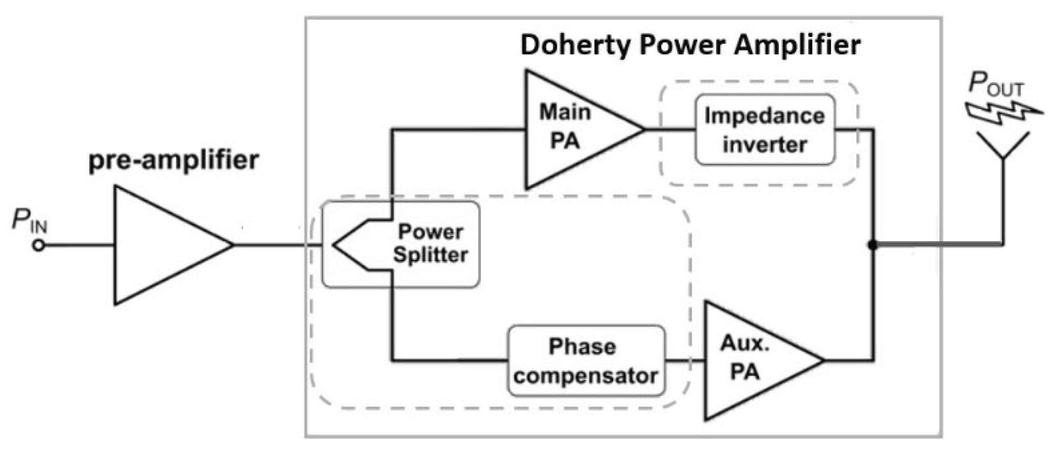
Figure 2.
Conceptual active load modulation in a two-way Doherty PA.
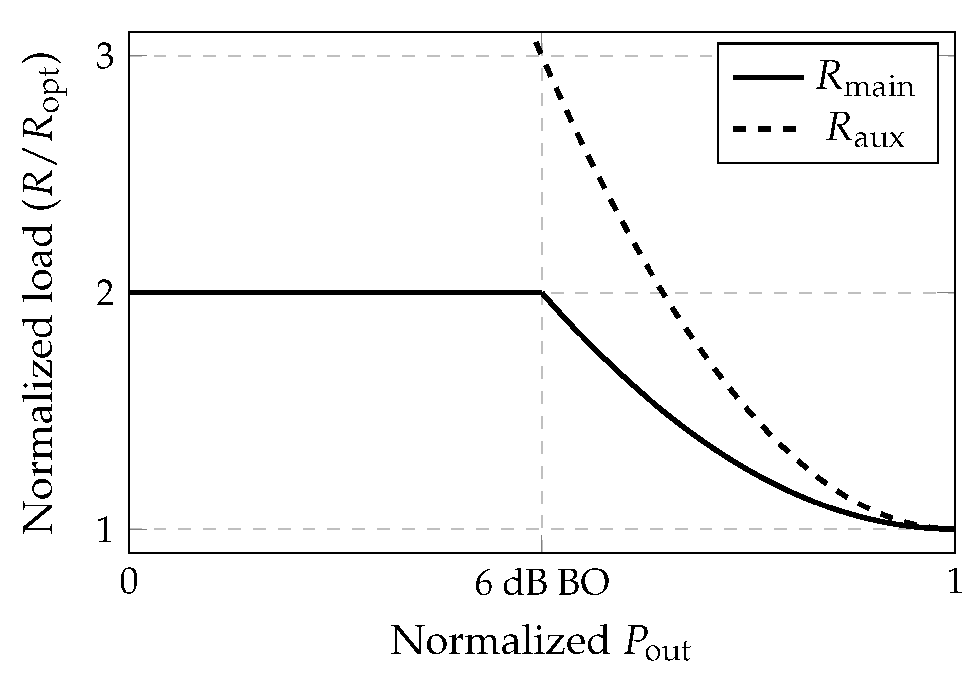
Figure 3.
Layout of the Quadrature Hybrid Combiner.
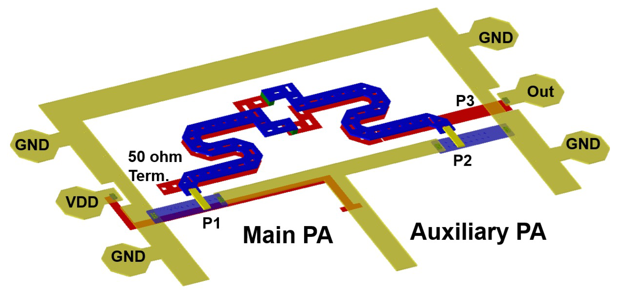
Figure 4.
Schematic diagram of the proposed DPA.
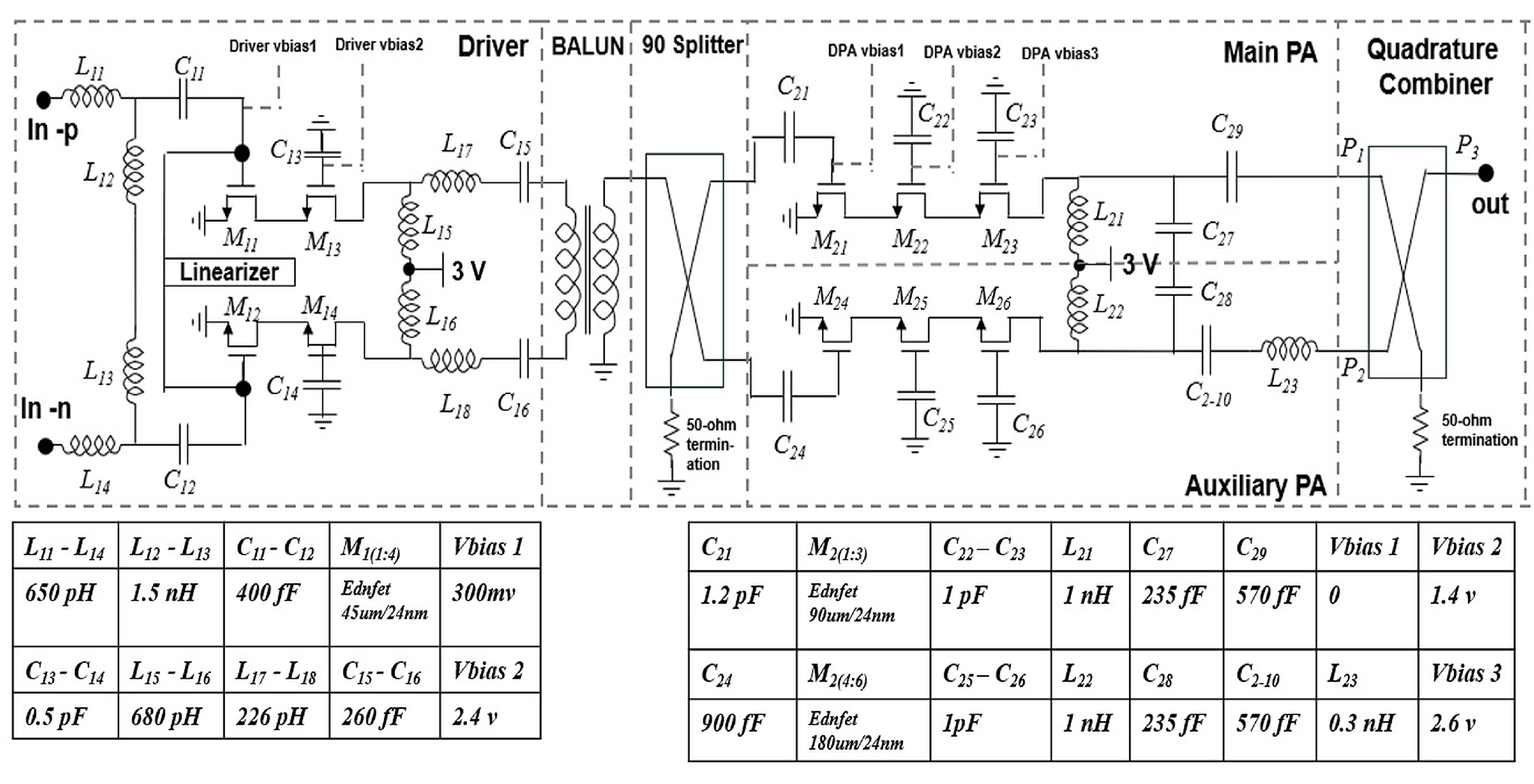
Figure 5.
Simulated Power–added efficiency at 10GHz versus output power. for a DPA with , DPA with , and Class B PA.
Figure 5.
Simulated Power–added efficiency at 10GHz versus output power. for a DPA with , DPA with , and Class B PA.
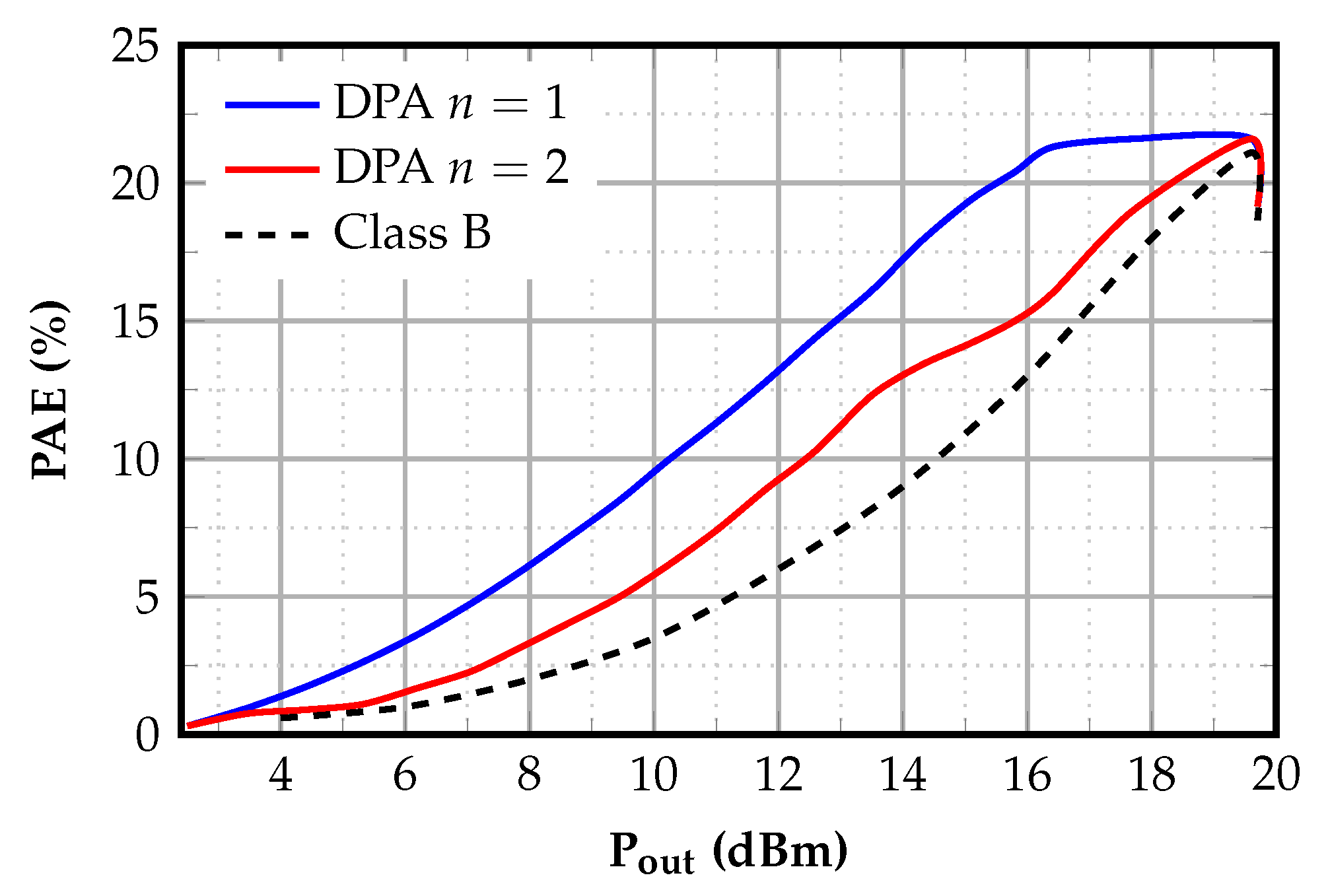
Figure 6.
DPA micrograph
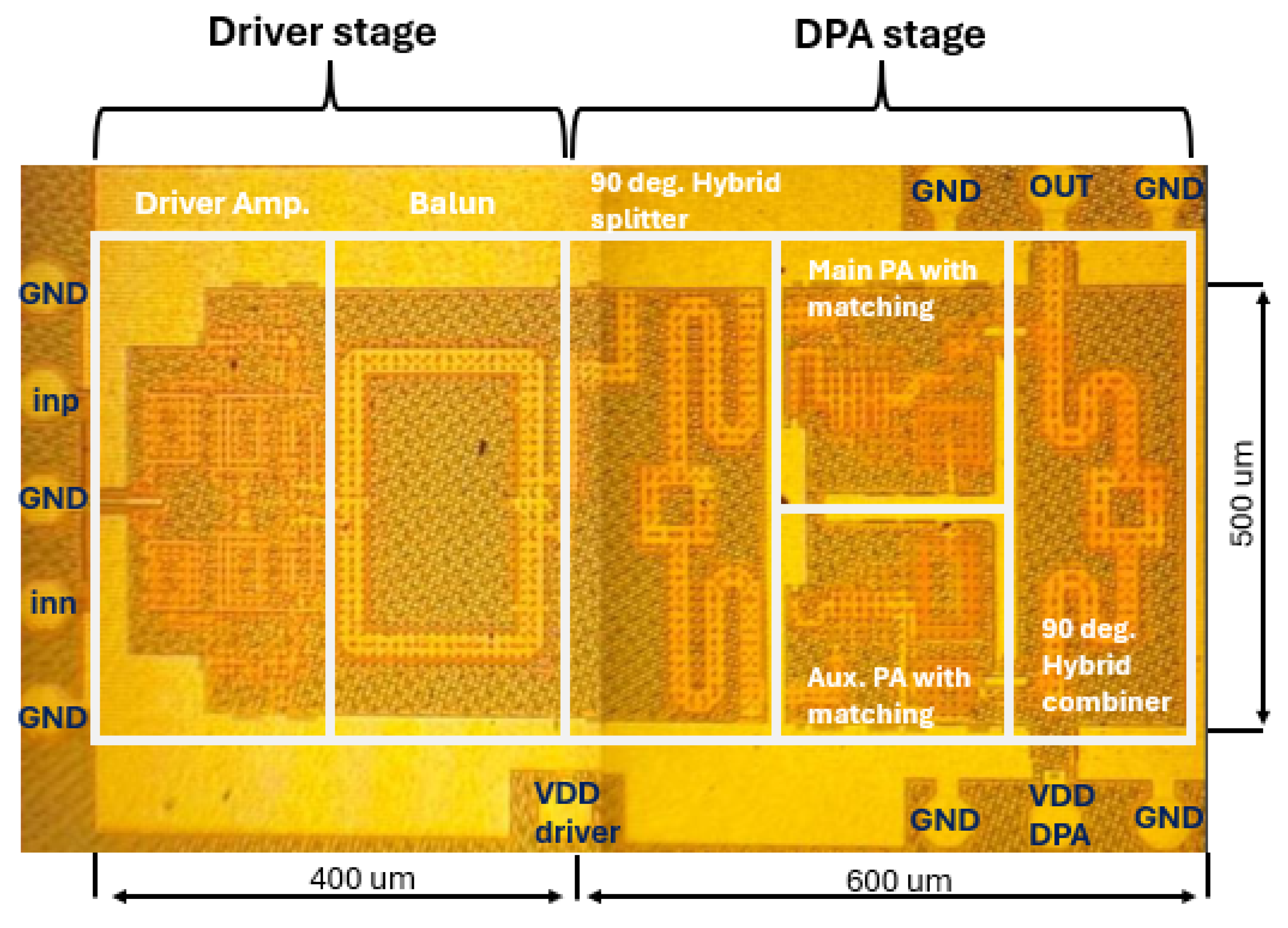
Figure 7.
Measured versus simulated , , and for the proposed DPA
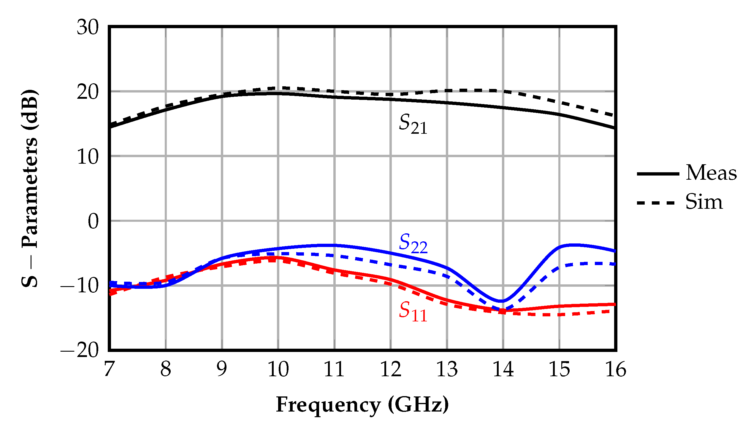
Figure 8.
Measured versus simulated PAE versus at 10GHz.
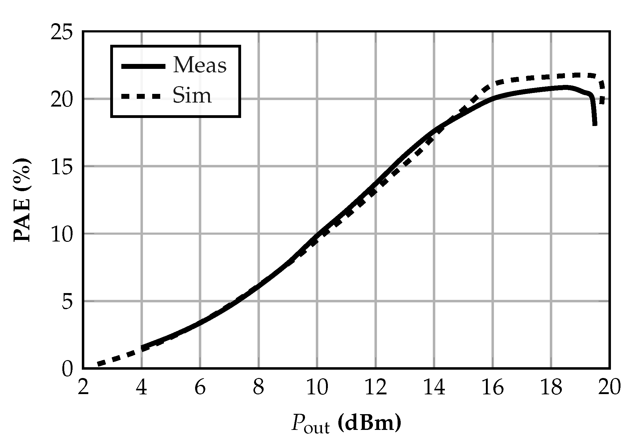
Figure 9.
Measured versus simulated across frequency.
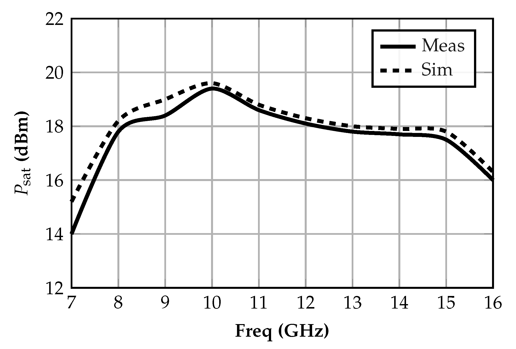
Figure 10.
Peak PAE versus frequency.
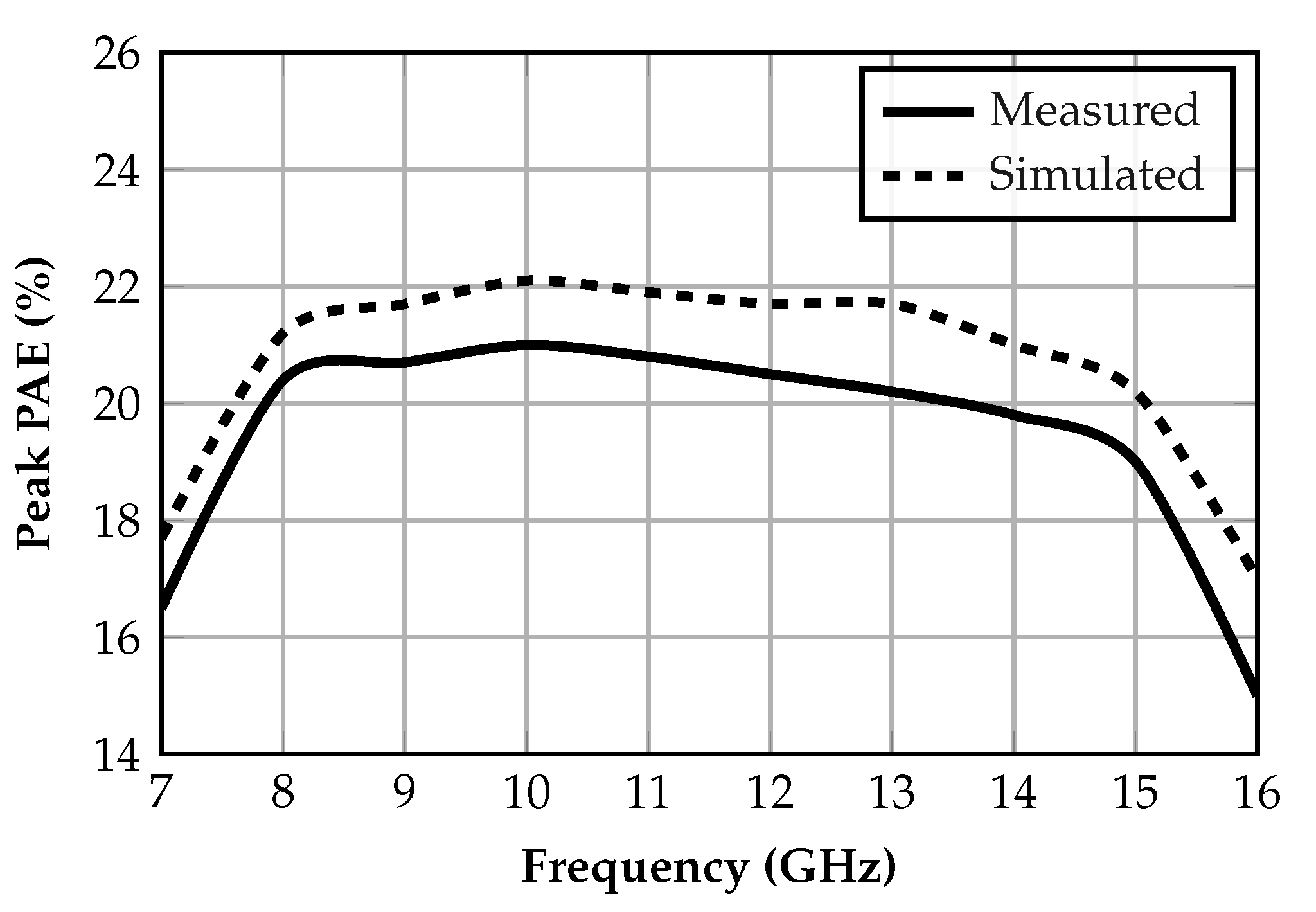
Figure 11.
Measured vs. simulated AM–AM at 10 GHz.
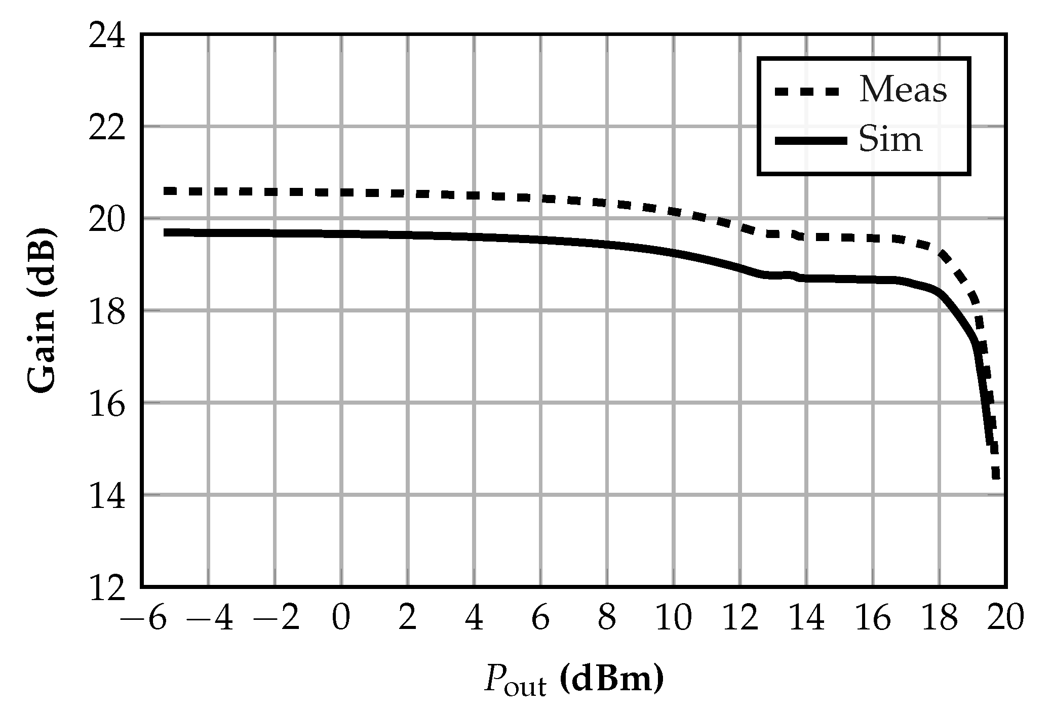
Figure 12.
AM–PM: normalized phase (degrees) versus output power (dBm).
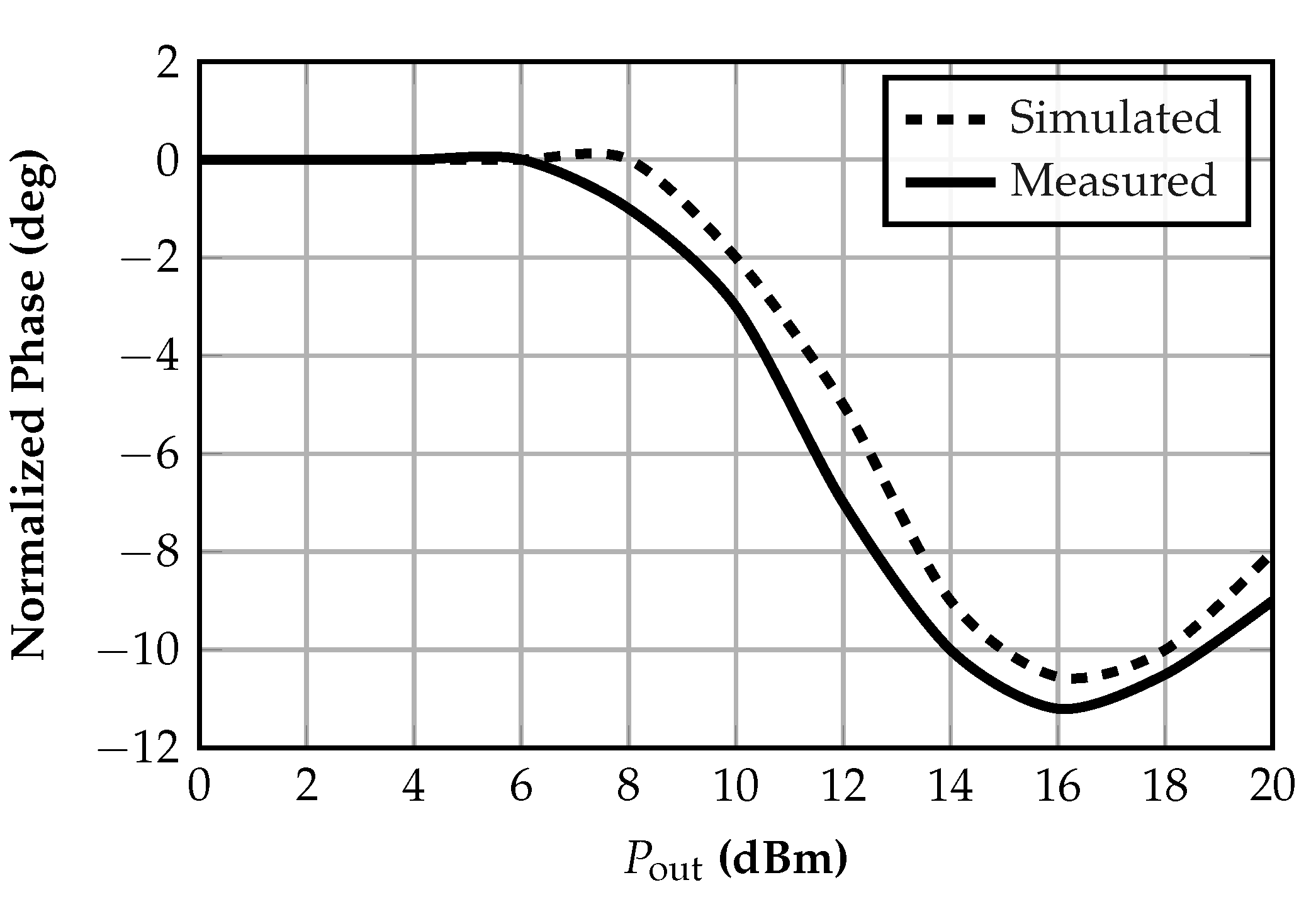
Figure 13.
Measured ACPR for 256 QAM SC
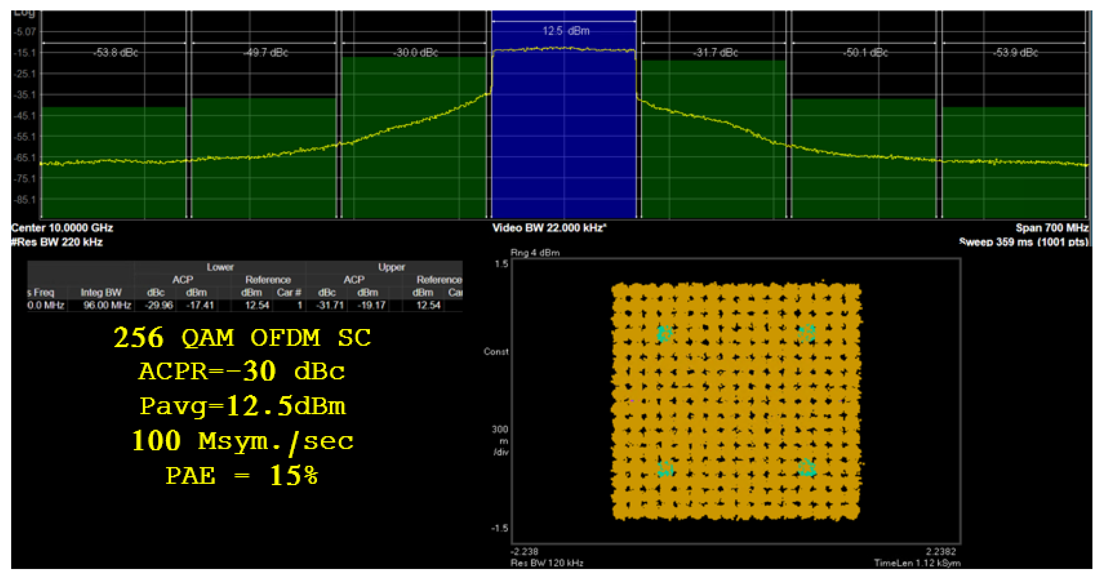
Figure 14.
Measured EVM (dB) versus for 100 MHz and 200 MHz modulation bandwidths.
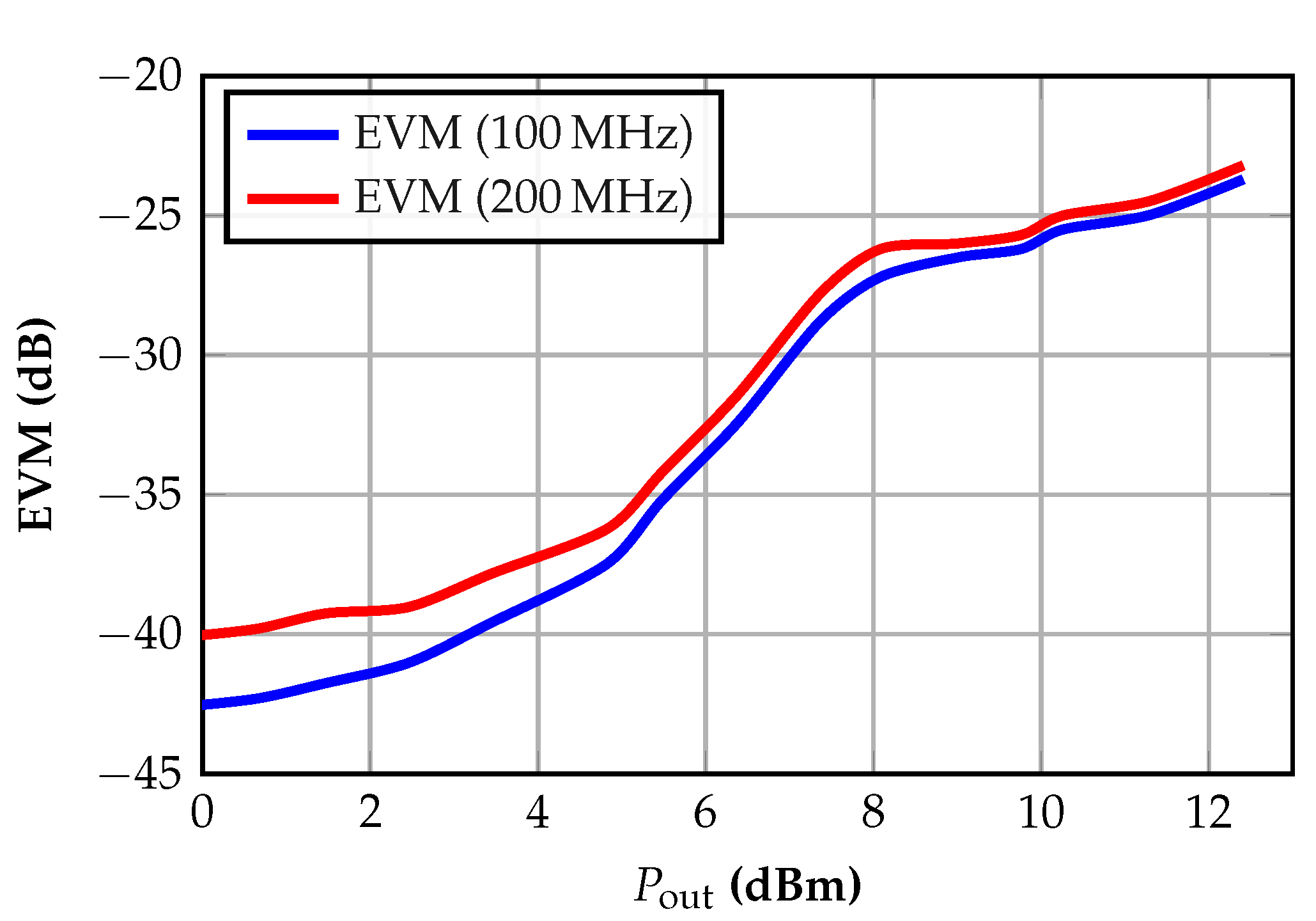

Table 1.
Comparison with state-of-the-art CMOS PAs
| Spec/Ref. | This work | [13]† | [14] | [15] | [16]† | [17]† |
|---|---|---|---|---|---|---|
| Technology | 22nm FD-SOI | 45 nm CMOS SOI | 65nm Bulk CMOS | 65nm Bulk CMOS | 22-nm FD-SOI | 28nm Bulk CMOS |
| Frequency () | 8–15 | 12-18 | 8.5-9.5 | 8–11.4 | 27–29 | 24.5-29.5 |
| FBW (%) | 61 | 40 | 11.1 | 35 | 7.1 | 18.5 |
| Gain () | 19.6 : 17 | 16 | 23.2 | 24.4 | 26.1 | 16.5 |
| Psat () | 19.5 | 25.5 | 20.9 | 20.5 | 22.5 | 18.8 |
| P1dB () | 18 | 25 | 16.5 | 15.2 | 21.1 | 17.5 |
| Peak PAE (%) | 21 | 31.9 | 24 | 24.5 | 28.5 | 30 |
| PAE (%) at 6 dB PBO | 17 | 23 | N/A | 9 | 22.1 | 20 |
| Supply (V) | 3 | 2 / 4.8 | 3.3 | 1.2 | 2.4 | 1.8 |
| Modulation | 256 QAM SC | 64 QAM SC | 256 QAM SC | N/A | 256 QAM SC | 64 QAM SC |
| Data rate (MSym/sec) | 100 | 200 | 600 | N/A | 800 | 100 |
| EVM (dB) | -24.3 | -25 | -35.9 | N/A | -30 | -25 |
| Pavg (dBm) | 12.5 | 16.4 | 12.7 | N/A | 10.2 | 12.4 |
| PAE at Pavg (%) | 15 | 15 | 4.58 | N/A | 9 | 20 |
| Die size () | 0.5 | 1 | 0.22 | 0.48 | 0.2 | 0.16 |
Entries annotated by † are DPAs, FBW with .
Disclaimer/Publisher’s Note: The statements, opinions and data contained in all publications are solely those of the individual author(s) and contributor(s) and not of MDPI and/or the editor(s). MDPI and/or the editor(s) disclaim responsibility for any injury to people or property resulting from any ideas, methods, instructions or products referred to in the content. |
© 2025 by the authors. Licensee MDPI, Basel, Switzerland. This article is an open access article distributed under the terms and conditions of the Creative Commons Attribution (CC BY) license (http://creativecommons.org/licenses/by/4.0/).
Copyright: This open access article is published under a Creative Commons CC BY 4.0 license, which permit the free download, distribution, and reuse, provided that the author and preprint are cited in any reuse.