
Submitted:
17 October 2025
Posted:
17 October 2025
You are already at the latest version
Abstract
This paper presents an FPGA-accelerated hybrid architecture for key-value stores (KVS) such as Memcached, designed to overcome latency and congestion challenges that arise in software-based distributed caching systems. By offloading the network and data-index layers to hardware logic within an FPGA, the proposed system reduces context-switch overhead, avoids retransmission-induced congestion loops, and achieves significant power efficiency. Experiments on a Xilinx Zynq-7000 SoC evaluation board demonstrate improved throughput and reduced power consumption compared to conventional kernel-based KVS architectures. This paper outlines the motivation, architecture, experimental results, and implications for scalable, low-latency caching infrastructure.Experiments on a Xilinx Zynq-7000 SoC evaluation board demonstrate improved throughput and reduced power consumption compared to conventional kernel-based KVS architectures. Note: This Technical Note was originally implemented and documented in 2013–2014. It has been revisited and republished in 2025 with updated links and references to preserve technical relevance.
Keywords:
FPGA
; key-value store
; memcached
; lwIP
; TCP offload engine
; hardware acceleration
; congestion control
1. Introduction
In large-scale web systems, in-memory key-value stores (KVS) such as Redis [8], Memcached [9], and Kyoto Tycoon [10] are widely adopted to reduce backend database load and improve response latency. These systems, often distributed through consistent hashing, serve as critical caching layers in web infrastructure. However, when deployed at scale, distributed KVS architectures exhibit limited congestion tolerance under heavy network load. As throughput increases, per-transaction latency also rises, leading to retransmission storms and system instability. Since this phenomenon originates below the application layer, it cannot be fully mitigated through software control.
The study proposes a hardware–software hybrid KVS, implemented on FPGA, to alleviate these issues. By partially offloading the networking and indexing operations to hardware, the system achieves deterministic latency and improved stability under congested conditions.
2. System Overview
2.1. Background
A KVS can be modeled as a simple key-value pair map, such as `std::map<string, string>`. Many implementations, including Google BigTable, Amazon SimpleDB, Apache Cassandra, and Azure Table Storage, are software-based. While these software KVS solutions support distributed operation and scalability, they suffer from the following limitations under high load:
- Increased context-switch overhead between threads/processes.
- Skewed key access leading to uneven node utilization.
- TCP retransmission loops, causing repeated ACK timeouts and congestion collapse.
Conventional scale-out designs exacerbate these issues by distributing the congestion rather than eliminating it.
3. Objective
The objective of this study is to propose and implement a hybrid hardware–software KVS that resolves these bottlenecks:
- Reduce context-switch cost.
- Prevent key hot-spot induced performance degradation.
- Eliminate TCP ACK timeout loops via hardware-level offload.
4. Architecture and Design
4.1. Concept: Hardware-Hybrid KVS
"Hardware-hybrid" refers to accelerating the bottleneck portions of the KVS software application through FPGA hardware logic. In this design, a Memcached-compatible KVS engine is extended with FPGA-based NIC caching and TCP Offload Engine (TOE) logic. The result is a system that combines software flexibility with hardware-level determinism and power efficiency, as illustrated in Figure .
4.2. Comparison with Existing FPGA-Based Memcached
Prior work on FPGA-accelerated Memcached includes Convey Computer’s hw-memcached [1], which employed a hybrid X86-FPGA appliance architecture. While both approaches leverage FPGA acceleration, the design philosophies and implementation strategies differ significantly.
Convey hw-memcached utilized high-end X86 processors paired with large-scale FPGA coprocessors in a rack-mounted appliance configuration. Their approach focused on offloading the entire Memcached workload to FPGA fabric, requiring significant hardware resources and sophisticated host-FPGA communication infrastructure. This results in high performance but at the cost of:
- High capital cost: Multi-FPGA cards and enterprise-grade server platforms.
- Complex integration: PCIe-based FPGA accelerators require host OS and driver stack.
- Power consumption: 3U appliance with 1670W power supply; estimated >500W system power.
- Deployment complexity: Requires specialized hardware procurement and maintenance.
In contrast, this study’s hybrid KVS adopts a lightweight, SoC-centric approach using Xilinx Zynq (ARM + FPGA), focusing on congestion mitigation and deterministic latency rather than raw throughput maximization:
- Low-cost platform: Single-chip SoC eliminates host CPU and reduces BOM cost.
- Minimal OS footprint: lwIP raw mode removes kernel overhead; no Linux/driver complexity.
- Power efficiency: 5–10W per node (50–100× lower than X86-FPGA appliances).
- Congestion-focused design: NIC-cache and simple TOE target retransmission loops, not just acceleration.
- Ease of deployment: Zynq evaluation boards support rapid prototyping without custom PCB design.
The key distinction lies in the design goal: Convey’s hw-memcached prioritized maximum throughput through full hardware implementation, while this hybrid KVS emphasizes congestion resilience, power efficiency, and deployment simplicity. By selectively offloading only the congestion-critical path (NIC-cache + TOE), the proposed system achieves stable performance under heavy load with minimal hardware complexity.
This trade-off makes the hybrid KVS suitable for edge deployment scenarios, embedded caching appliances, and cost-sensitive distributed systems where power and complexity constraints dominate performance requirements.
4.3. NIC-Cache and Simple TOE
A small, FPGA-embedded cache region is directly connected to the network interface (NIC). This mechanism mitigates hot-spot key access by enabling near-NIC caching and early response before entering the software TCP/IP stack. It effectively prevents retransmission loops triggered by ACK delays—one of the major causes of congestion in software-based systems. When a cache miss occurs, the request is routed to the software stack (Figure 1). On a cache hit, the FPGA responds directly via the NIC cache without software intervention (Figure 2).
4.4. Lightweight Stack: lwIP (Raw Mode)
The software stack runs in a minimal configuration using lwIP (lightweight TCP/IP) in raw mode, coupled directly with the database module. By excluding the kernel (e.g., mutexes, pthreads, file systems), context switching is drastically reduced. This yields a deterministic execution environment where each request follows a fixed, low-latency path from network ingress to database lookup [2].
4.5. Software–Hardware Boundary
The hybrid KVS defines a clear boundary between software and hardware processing, as shown in Figure 3:
- Software region: TCP server (lwIP), packet parser, and API layer.
- Hardware region: Memory burst controller, DMA interface, and index search logic.
FPGA modules handle database index operations (search/insert/delete) using DMA streams, while the ARM processor executes higher-level protocol control. The FPGA is designed to tolerate duplicate index values for concurrent operations, improving access concurrency.
To ensure uniform latency under parallel request load, the design employs an AXI Multi-Ported Memory Controller (MPMC) [3]. The MPMC arbitrates multiple DMA ports accessing DDR3 memory in parallel, enabling concurrent burst transactions from independent FPGA logic blocks. This architecture prevents memory contention-induced latency spikes that typically occur in single-port designs under concurrent access.
By distributing memory bandwidth across multiple AXI ports, the system maintains deterministic read/write latency even when multiple index lookup operations execute simultaneously. This is critical for sustaining low-latency responses during traffic bursts, where conventional single-channel memory interfaces would introduce serialization delays.
4.6. Index Normalization
In conventional KVS designs, a key maps to a unique index—resulting in high search cost and collision risk. The hybrid KVS introduces a non-normalized index, where multiple records may share a hash-based key index. FPGA logic filters these candidates in parallel, checking actual key values through a lightweight string comparison. This transformation converts serial index lookup into parallel DMA streaming, improving throughput.
4.7. Congestion Reduction Mechanism
Most KVS systems depend on TCP/IP at the network layer. In distributed configurations, key skew can cause excessive load on specific nodes. The proposed hybrid KVS introduces FPGA-based congestion mitigation by intercepting Ethernet frames before they enter the lwIP stack. NIC–FPGA logic identifies frequently accessed keys and returns cached responses immediately, while updating sequence numbers to maintain TCP session integrity. This approach breaks the feedback loop that normally triggers ACK storms and retransmissions, as illustrated in Figure 4.
4.8. Context Switch Analysis
In conventional multi-core OS environments, each data request involves multiple context switches (network thread -> kernel -> database thread). As data count increases, this overhead grows linearly. In contrast, the hybrid KVS eliminates nearly all context switching by maintaining direct, event-driven execution between lwIP and the FPGA database module, as illustrated in Figure 5.
5. Evaluation and Results
5.1. Experimental Setup
The prototype was implemented on a Xilinx Zynq-7000 SoC (ZC706 Evaluation Kit) [4] with lwIP as the TCP/IP stack. Evaluation tests simulated 200,000 randomly generated records. Randomized set:get ratios of 2:8 were used for load measurement.
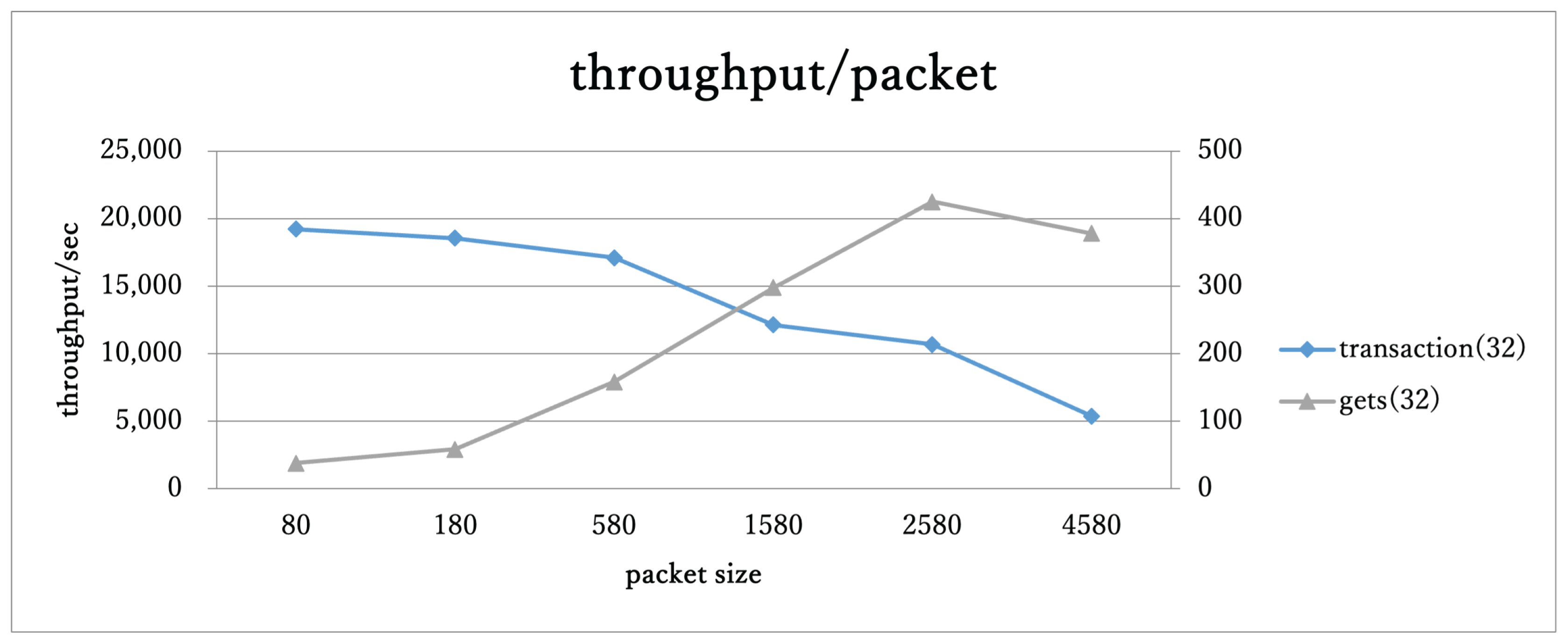
5.2. Random Access Performance
Throughput was measured in transactions per second (TPS) and throughput per packet (Mbps). Peak efficiency was observed when the packet size approached the Ethernet frame limit, 1518 bytes. Even without NIC-cache hits, the hybrid KVS achieved stable transaction throughput, with a 10% cache hit rate, total throughput increased by 10%, reaching 20,000 TPS / 480 Mbps, as shown in Figure 6.
5.3. Unit-Level Comparison
A 1U system (500W power budget) equipped with 24 hybrid KVS boards was compared to a conventional Xeon-based memcached cluster, as summarized in Figure 7.

Table 1.
Unit-Level Performance Comparison
| Metric | memcached (Xeon) | Hybrid KVS (FPGA) |
|---|---|---|
| TPS | 4,744 | 5,943 |
| Throughput (Mbps) | 4055 | 5943 |
| Error rate | High (timeouts) | None detected |
| Power per node | ∼62.5W | 5–10W |
5.4. Power Efficiency
Power consumption was reduced by more than 10 × per KVS instance. This directly translates into substantial operational cost savings in large-scale distributed cache deployments, particularly in data centers where energy efficiency is critical.
6. Discussion
The results demonstrate that hybridizing software KVS with FPGA logic significantly enhances reliability and scalability. By redefining the boundary between application, protocol stack, and hardware, the design effectively suppresses congestion propagation and TCP retransmission loops. Furthermore, the energy efficiency of the system suggests that FPGA-accelerated caching may become a key element in future low-latency web architectures.
At the time of development (2013–2014), only Xilinx Zynq SoCs supported this level of integration. However, with the later release of Intel (Altera) SoCs, similar hybrid KVS designs could be ported for broader evaluation.
This work anticipates trends later adopted in cloud-edge acceleration, where FPGA-assisted NICs (SmartNICs) and hardware offload engines have become industry standards.
7. Related Work
7.1. FPGA-Based Near-Memory
While the FPGA-Based Near-Memory Acceleration of Modern Data-Intensive Applications by Singh et al. [5] focuses on HBM-based near-memory computation, this study represents an earlier implementation (in fiscal year 2013) of a “Near-NIC Computing” architecture that consolidated the data path into FPGA logic placed near the network I/O hierarchy. The proposed FPGA-Hybrid KVS integrated NIC caching, TCP offload, and index lookup on an ARM–FPGA SoC, achieving 10× higher power efficiency than conventional CPU-driven KVS by suppressing communication latency and congestion retransmission at the physical layer. This design served as an early demonstration of minimizing data movement, a concept later inherited by SmartNIC and HBM-based near-memory computing architectures.
7.2. Plug and Offload: Transparently Offloading TCP Stack onto Off-path SmartNIC with PnO-TCP
Recent work by Nan et al. (2025) introduced Plug and Offload (PnO), a transparent TCP stack offloading framework that executes the entire TCP protocol stack on off-path SmartNICs (specifically, NVIDIA BlueField DPUs) without any application modification [6]. PnO-TCP, the core component of their framework, is a lightweight user-space TCP stack built on DPDK and optimized for ARM-based DPU cores. It employs PCIe DMA-based message rings to enable seamless communication between the host and the SmartNIC, achieving transparent TCP execution. Their evaluation using real-world applications such as Redis, Lighttpd, and HAProxy demonstrated significant CPU utilization reduction and performance improvement—up to 127% throughput gain for small packet workloads (<2KB).
In contrast, the present work by Sugisawa (2013) represents an earlier and on-chip realization of TCP offloading and near-network computation more than a decade before PnO-TCP. Our design integrates a hardware-embedded NIC cache and a simplified TCP Offload Engine (TOE) directly within a Xilinx Zynq SoC, coupling the FPGA fabric with ARM processors via the AXI interconnect. Furthermore, the system implements DMA-based parallel index operations for a Memcached-compatible key-value store, forming an early prototype of what can now be termed a Near-I/O Computing Architecture.
Whereas PnO-TCP focuses on off-path SmartNICs and transparent software compatibility through PCIe-based message passing, our system realizes an on-chip, on-path integration emphasizing deterministic latency, congestion resilience, and low power consumption. The FPGA logic layer directly intercepts TCP ACK loops and retransmission storms, preventing congestion collapse at the physical layer—an issue that PnO-TCP still mitigates in software.
Therefore, PnO-TCP can be regarded as a cloud-scale extension of the design principles demonstrated in our earlier FPGA-SoC-based hybrid architecture. Both studies address the same fundamental challenge—reducing TCP processing overhead while maintaining latency stability—but from complementary perspectives. Our work stands as an early embodiment of near-I/O and on-chip TCP offloading, predating SmartNIC- and DPU-based research such as FlexTOE and PnO-TCP, and providing an architectural foundation for subsequent offload frameworks targeting network–application co-design.
7.3. FPGA-Based Near-Memory Acceleration of Modern Data-Intensive Applications
Recent work by Zhang et al. (2021) presents a high-throughput parallel hash table design for FPGAs using XOR-based multi-ported memory [7]. Their architecture achieves deterministic throughput for all hash table operations—search, insert, update, and delete—by employing multiple Processing Engines (PEs) with XOR-encoded on-chip memories, thus eliminating data-dependent performance degradation. The design scales up to 16 PEs and attains 5,926 MOPS on Xilinx Alveo U250, surpassing the performance of prior FPGA-based hash tables such as FASTHash while maintaining full functionality and consistency across replicas. This work represents an important advancement in near-memory computing by maximizing the utilization of on-chip SRAM bandwidth to support fully parallelized key-value access. In contrast, our earlier work (Sugisawa, 2013) demonstrated an on-chip hardware–software hybrid architecture that integrates the network transport layer and key-value indexing logic within a Xilinx Zynq SoC. By embedding a NIC cache and a lightweight TCP Offload Engine (TOE) directly in FPGA fabric, and connecting them to the ARM processor through AXI DMA and multi-ported memory controllers, our system achieves deterministic low latency and congestion-free communication under heavy network load. Unlike Zhang et al.’s design—which focuses on intra-chip parallelism of memory operations—our work emphasizes inter-layer fusion, unifying the TCP/IP stack and application logic at the hardware level to suppress retransmission loops and eliminate kernel-level scheduling overhead. Conceptually, the two studies tackle complementary dimensions of near-memory computing: Zhang et al. optimize intra-FPGA memory concurrency, while our hybrid KVS explores near-network dataflow computation within a SoC-integrated FPGA. Notably, our design predates the emergence of SmartNIC and DPU architectures by over a decade, providing an early prototype of near-I/O computing that tightly couples communication, indexing, and caching within a single hardware substrate. From today’s perspective, the FPGA-Hybrid KVS can be regarded as a foundational precursor to modern near-memory accelerators such as XOR-based FPGA hash tables and SmartNIC-enabled key-value systems.
8. Conclusion
This study demonstrated a practical implementation of an FPGA-accelerated hybrid KVS that maintains Memcached protocol compatibility while resolving the key bottlenecks of software-based distributed caching systems.
The design achieves:
- Reduced context-switch latency.
- Improved congestion resilience.
- Deterministic low-latency performance.
- Up to 10 × power efficiency gain.
Future work includes:
- Rebuilding and evaluating the design on newer SoCs (Zynq Ultrascale, Intel Agilex).
- Deploying in real-world caching scenarios such as chat engines and session stores.
- Exploring patent protection for the hardware–software boundary and TOE module.
References
- Convey Computer Corporation, “Convey Revs Memcached with Hybrid X86-FPGA Appliance,” AI Wire, Sep. 2013. https://www.aiwire.net/2013/09/24/convey-revs-memcached-hybrid-x86-fpga-appliance/.
- lwIP - A Lightweight TCP/IP Stack, Savannah - GNU Project. https://savannah.nongnu.org/projects/lwip/.
- AMD (Xilinx), “AXI Multi-Ported Memory Controller (MPMC),” XAPP739 Application Note. https://docs.amd.com/v/u/en-US/xapp739_axi_mpmc.
- AMD (Xilinx), “Zynq-7000 SoC ZC706 Evaluation Kit,” Product Specification. https://www.amd.com/en/ products/adaptive-socs-and-fpgas/evaluation-boards/ek-z7-zc706-g.html.
- G. Singh, M. Alser, D. S. Cali, D. Diamantopoulos, J. Gomez-Luna, H. Corporaal, and O. Mutlu, “FPGA-Based Near-Memory Acceleration of Modern Data-Intensive Applications,” IEEE Micro, vol. 41, no. 4, pp. 39–48, Jul. 2021, . [CrossRef]
- H. Nan, Z. Zhe, and M. Yang, “Plug & Offload: Transparently Offloading TCP Stack onto Off-path SmartNIC with PnO-TCP,” arXiv preprint arXiv:2503.22930v1, Mar. 2025. https://arxiv.org/pdf/2503.22930v1.
- R. Zhang, S. Wijeratne, Y. Yang, S. R. Kuppannagari, and V. K. Prasanna, “A High Throughput Parallel Hash Table on FPGA using XOR-based Memory,” arXiv preprint arXiv:2108.03390v2, Aug. 2021. https://arxiv.org/pdf/2108.03390.
- Salvatore Sanfilippo and Pieter Noordhuis, Redis: An open source, in-memory data structure store, Available at: https://redis.io/, 2009.
- Brad Fitzpatrick et al., Memcached: A distributed memory object caching system, Available at: https://memcached.org/, 2003.
- FAL Labs, Kyoto Tycoon: A lightweight network DBM server with a scriptable interface, 2011. Available at: https://dbmx.net/kyototycoon/.
Figure 1.
Cache miss: request routed to software stack.
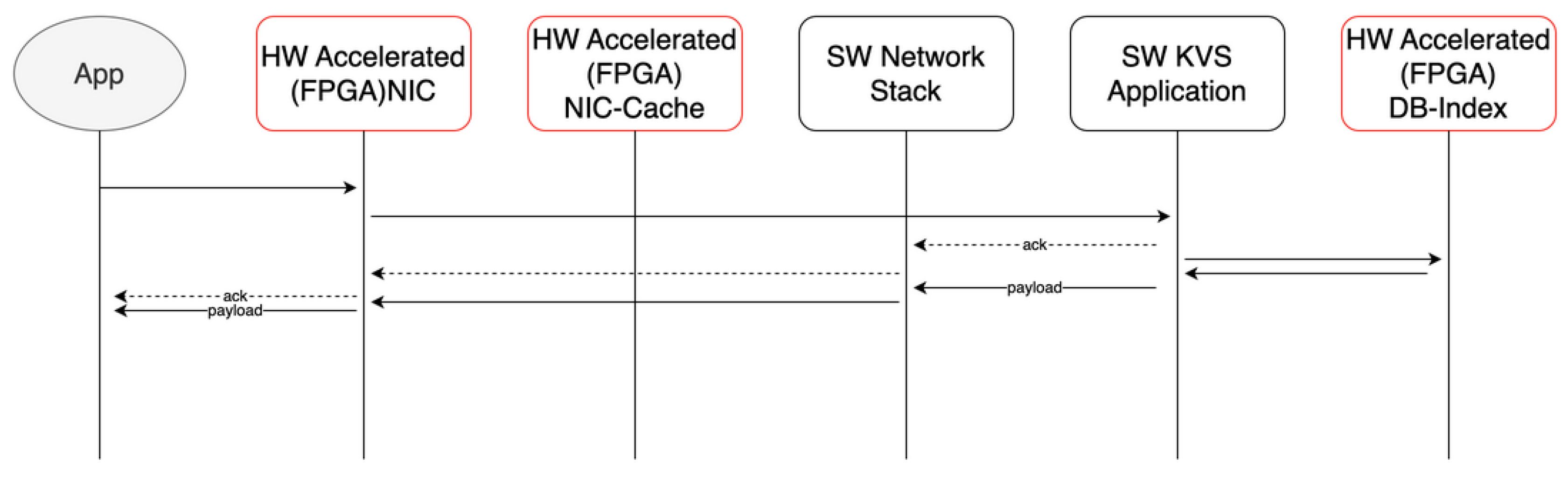
Figure 2.
Cache hit: direct FPGA response via NIC cache.
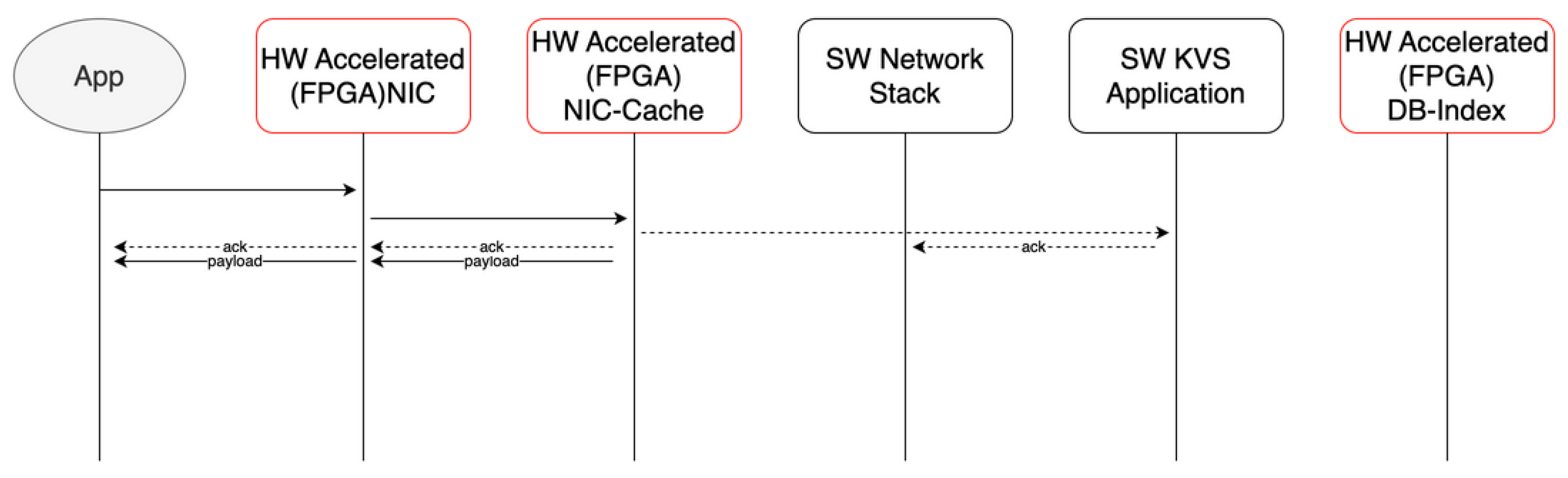
Figure 3.
Software–Hardware Boundary in Hybrid KVS (Zynq ARM + FPGA)
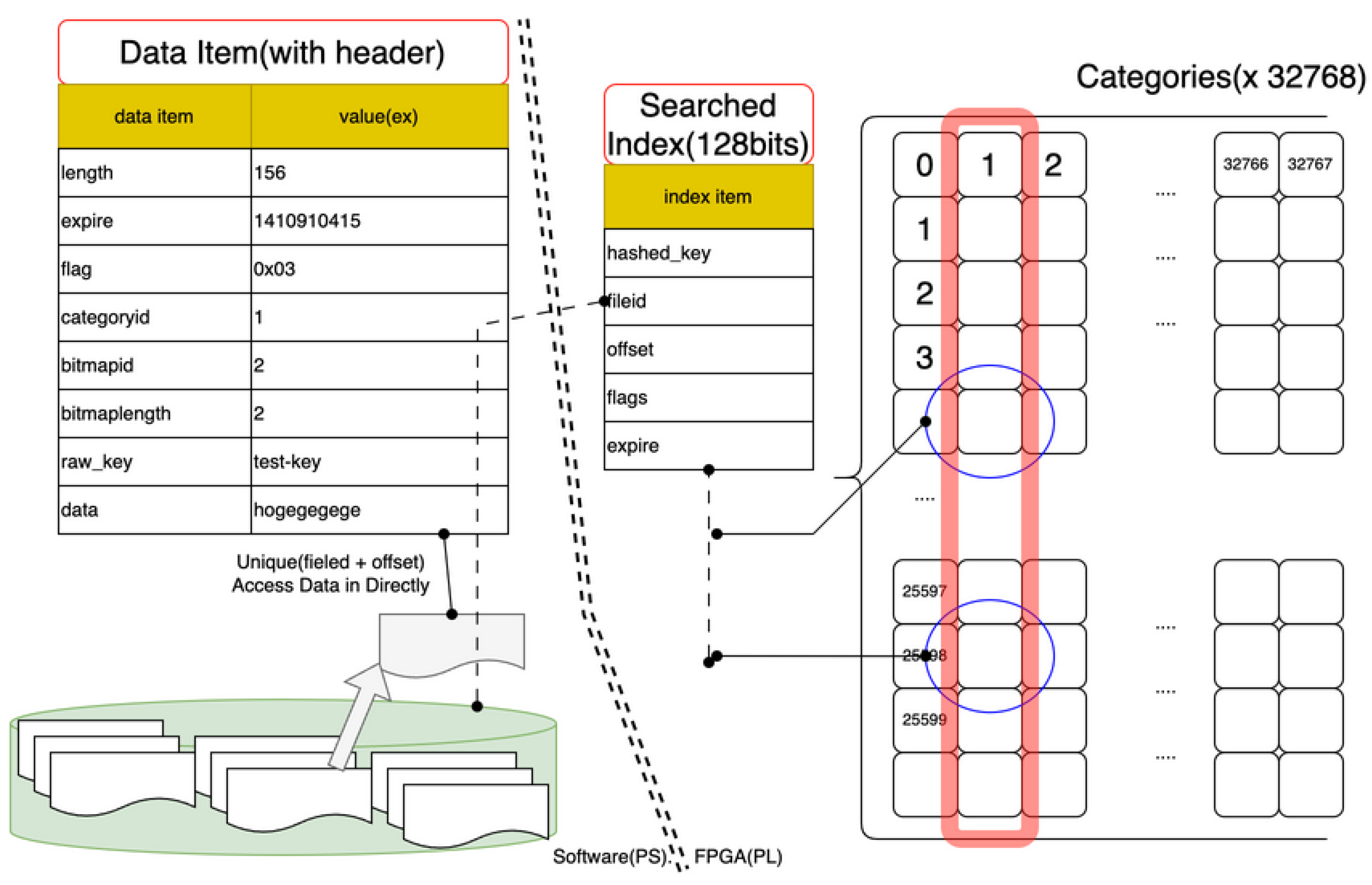
Figure 4.
NIC Cache Congestion Reduction Flow
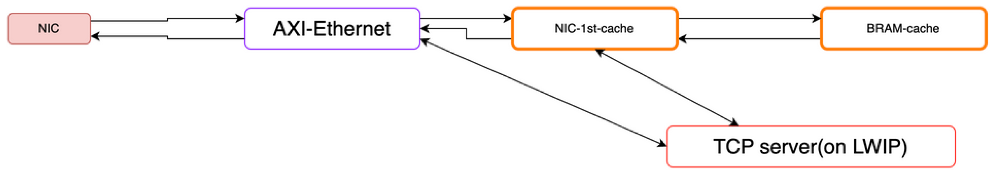
Figure 5.
Context switch comparison: Software KVS vs. Hybrid KVS
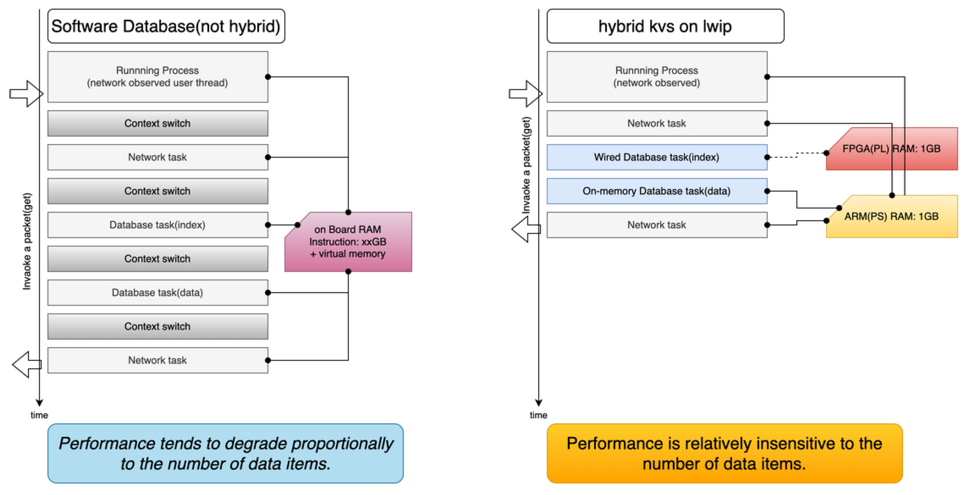
Figure 6.
Throughput vs. Packet Size (Hybrid KVS)
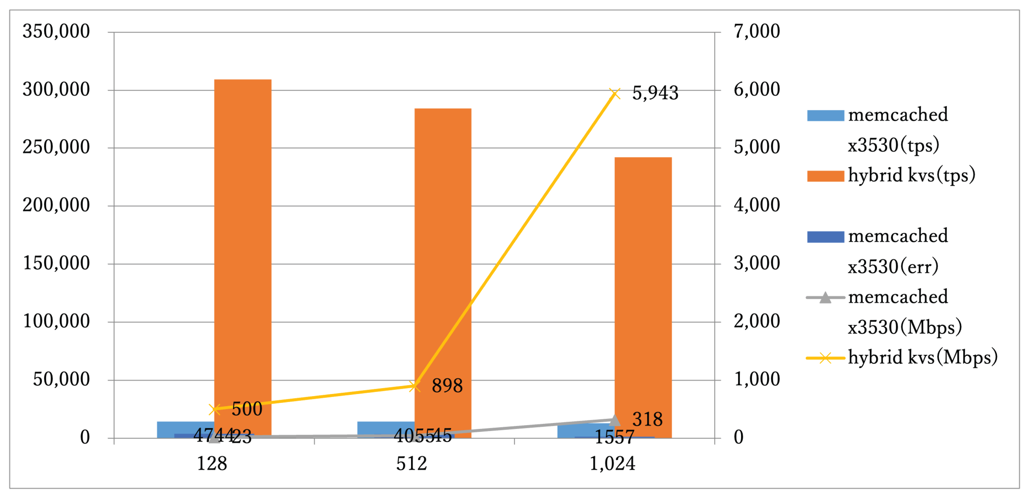
Figure 7.
Unit-Level Performance Comparison
Disclaimer/Publisher’s Note: The statements, opinions and data contained in all publications are solely those of the individual author(s) and contributor(s) and not of MDPI and/or the editor(s). MDPI and/or the editor(s) disclaim responsibility for any injury to people or property resulting from any ideas, methods, instructions or products referred to in the content. |
© 2025 by the authors. Licensee MDPI, Basel, Switzerland. This article is an open access article distributed under the terms and conditions of the Creative Commons Attribution (CC BY) license (http://creativecommons.org/licenses/by/4.0/).
Copyright: This open access article is published under a Creative Commons CC BY 4.0 license, which permit the free download, distribution, and reuse, provided that the author and preprint are cited in any reuse.


