
Submitted:
15 July 2025
Posted:
16 July 2025
You are already at the latest version
Abstract
This work investigates the effect of interface traps on the impedance spectra of dopant-free silicon solar cells. The studied device consists of a crystalline silicon absorber with an a-Si:H/MoOx/ITO stack as the front passivating hole-collecting contact and an a-Si:H/LiF/Al stack as the rear passivating electron-collecting contact. Experimental measurements, including illuminated current–voltage (I–V) characteristics and impedance spectroscopy, were performed on the as fabricated devices and after a soft annealing treatment. The annealed cells exhibit an increased open-circuit voltage and a larger Nyquist plot radius. To interpret these results, a numerical model was developed in a TCAD environment. Simulations reveal that traps located at the p/i interface (MoOx/i-a-Si:H) significantly affect the impedance spectra, with higher trap concentrations leading to smaller Nyquist plot circumferences. The numerical impedance curves were aligned to the experimental data, enabling extraction of the interfacial traps concentration. The results highlight the sensitivity of impedance spectroscopy to interfacial quality and confirm that the performance improvement after soft annealing is primarily due to reduced defect density at the MoOx/i-a-Si:H interface.
Keywords:
impedance spectroscopy
; TCAD
; annealing
; Nyquist plot
; dopant-free
; silicon solar cells
1. Introduction
Impedance spectroscopy (IS) is an alternating current (AC) characterization technique that allows the detailed investigation of physical mechanisms dominating the device under test (DUT). AC-based techniques are particularly effective in supporting device optimization, as they provide comprehensive information on charge transport and recombination dynamics. Among these techniques, IS offers significant advantages due to its capability to probe the physical phenomena occurring across the different layers of a multilayered structure by accessing only the external terminals of the DUT [1,2,3,4,5,6,7,8]. From IS data, it is possible to extract several key parameters, including interface quality and the presence of parasitic junctions within the device architecture [9,10,11,12,13]. Typically, impedance data are represented through Nyquist plots, which facilitate the derivation of an equivalent circuit model [14] describing the dynamic behavior of the DUT, such as a solar cell.
High-efficiency photovoltaic (PV) devices rely on three fundamental processes: efficient photogeneration of electron-hole pairs, spatial separation of charge carriers, and their selective extraction at the respective electrodes. In Silicon (Si)-based solar cells, which currently dominate the PV market, the availability of high-quality Si wafers ensures effective carrier photogeneration. Consequently, overall device efficiency is predominantly governed by the selectivity and effectiveness of the contact interfaces. At both the laboratory and industrial levels, selective contacts are typically realized through heavy doping of crystalline Silicon (c-Si) by means of dopant diffusion, as in the homojunction-based passivated emitter and rear cell (PERC) architecture [15]. Alternatively, in Silicon heterojunction (SHJ) solar cells, intrinsic and doped hydrogenated amorphous Silicon (a-Si:H) thin films are deposited on both surfaces of the c-Si wafer [16]. This configuration is particularly attractive, as it avoids high-temperature (>800 °C) diffusion processes and enables excellent electronic decoupling between the c-Si absorber and metal electrodes, resulting in high open-circuit voltages and record device efficiencies [17].
Despite the advantages offered by SHJ cells employing doped a-Si:H layers, they face certain limitations. The front-side doped layer is associated with parasitic absorption, thereby reducing the maximum achievable photocurrent [18,19,20], and its fabrication via plasma-enhanced chemical vapor deposition (PECVD) requires hazardous precursor gases. To overcome these limitations, alternative wide-bandgap materials processed at low temperatures through methods such as thermal evaporation or solution-based techniques are being investigated as potential replacements for doped silicon. Promising candidates include metal oxides [21,22], fluorides [23,24], sulfides [25], and organic semiconductors [26,27].
In this context, the development of dopant-free silicon solar cells has gained significant attention over the past decade [28]. Recent advances have demonstrated power conversion efficiencies exceeding 23% [29], with a record efficiency of 23.83% reported for a device employing an ultrathin Molybdenum oxide (MoOx) layer as a hole-selective contact, achieved through interfacial engineering at the a-Si:H/MoOx junction [30]. These dopant-free architectures are attractive due to their simplified fabrication processes, the elimination of high-temperature doping steps, and potential compatibility with flexible or temperature-sensitive substrates. However, the electrical performance of dopant-free contacts currently remains inferior to that of conventional doped interfaces, primarily due to their lower technological maturity. Achieving high levels of surface passivation and charge selectivity continues to represent a critical challenge, necessitating optimized process development. Furthermore, the physical origins of performance limitations are often linked to interfacial phenomena that are not yet fully understood.
In this work, we investigate impedance spectroscopy as a technique to provide insights into the quality of specific interfaces in dopant-free solar cells where MoOx is used on the front side as hole transport layer and Lithium fluoride (LiF)/Aluminium (Al) is used at the rear side for electron collection. In Section 2, we describe the structure of the experimental device and detail its fabrication process and the performed soft annealing treatment. Section 3 presents experimental measurements of current–voltage (I-V) characteristics under illumination and impedance spectroscopy data acquired both on the as-fabricated cells and after the soft anneal. In Section 4, we introduce a numerical model built in Sentaurus TCAD to interpret trends in experimental Nyquist data. The model is calibrated using the experimental data consisting of both I-V characteristics and impedance spectra obtained on the DUT as fabricated and after the soft anneal. Through this modelling approach, we extract the defect concentration at a targeted interface before and after soft anneal, providing a quantitative link between the electrical response and interfacial properties. Finally, Section 5 presents the main conclusions of this study.
2. Solar Cells Fabrication
The schematic structure of the solar cells under investigation is presented in Figure 1. Front-emitter devices with an active area of 4 cm2 were fabricated using flat, float-zone (FZ) crystalline silicon (c-Si) wafers with n-type <100> orientation, a resistivity of 1–5 Ω·cm, and a thickness of 270 μm. Surface passivation was achieved by depositing intrinsic a-Si:H layers via PECVD at a standard frequency of 13.56 MHz. The a-Si:H layers had thicknesses of 5 nm and 7 nm on the front and rear surfaces, respectively. Thermally evaporated MoOx and LiF/Al layers were subsequently applied to serve as selective hole and electron contacts, respectively.
The MoOx films were grown by thermal evaporation of high-purity stoichiometric MoO3 powder (99.95%) at a deposition rate of 1 Å/s from a tungsten boat, under a base pressure below 4 × 10⁻⁷ mbar [31]. No intentional substrate heating was applied during evaporation, allowing the substrate to remain near ambient temperature. Similarly, the LiF layers were thermally evaporated from 99.95% pure stoichiometric powder at a rate of 0.2 Å/s under the same vacuum conditions.
The LiF layer had a nominal thickness of approximately 1 nm and was capped with a full-area 100 nm-thick aluminum layer. The front-side MoOx layer was 8 nm thick and was overlaid with a 80 nm-thick indium tin oxide (ITO) transparent conductive oxide (TCO) deposited via RF sputtering, followed by the deposition of a 5 μm-thick aluminum collection grid.
Layer thicknesses were determined using variable-angle spectroscopic ellipsometry (VASE, J.A. Woollam Co., Lincoln, NE, USA). The ITO layer was deposited using an RF-sputtering system (Material Research Corporation, MRC mod. 643) operating at 13.56 MHz in argon plasma. Deposition conditions were set to 3.4 mTorr pressure and a power density of 0.88 W/cm2, using a tin-doped indium oxide (In2O3:Sn, 10 wt%) target. The resulting ITO film exhibited a sheet resistance of 54 Ω/sq.
It is well established that chemical passivation can degrade following TCO deposition due to plasma-induced effects, including luminescence and possible ion bombardment [32]. In SHJ devices utilizing doped silicon layers, the electronic quality of the interface can typically be recovered via thermal annealing at 180–200 °C for 30 minutes [33]. However, such treatments may be detrimental when MoOx is employed as the hole-selective layer, necessitating the exploration of alternative thermal processes [34]. In this work, a soft annealing procedure consisting of a 10-minute treatment at 100 °C on a hot plate in ambient air was evaluated.
3. Experimental Results
3.1. Current-Voltage Characteristics
The solar cells were characterized before and after the soft annealing by collecting both current-voltage characteristics and impedance data. The illuminated current-voltage (J-V) characteristics under AM1.5G spectrum were measured with a WACOM class AAA dual-lamp solar simulator. The results are shown in Figure 2. From this graph, it can be noted that the device after soft annealing treatment (red line in Figure 2) has a higher open circuit voltage, VOC, with respect to the device as fabricated (blue line in the same figure). This outcome could be in principle attributed to the recovery of chemical passivation [39].
3.2. Impedance Spectroscopy
Impedance was monitored using a Solartron 1260 Impedance Analyzer under illumination, employing the same solar simulator used for the I-V characteristics described in the previous section. Frequency was swept from 1 MHz to 100 mHz with a logarithmic sweep. The considered AC stimulus amplitude was set to 100 mV, while the DC bias was changed from 0 V to 1 V in steps of 0.2 V. IS data are commonly represented in the form of Nyquist plots. In these graphs the real part of the measured impedance is represented on the x-axis while the imaginary part is shown in the y-axis. Every point is taken for a certain frequency, while each curve is related to a given DC bias. In this work, the impedance data are shown in the form of 3D Nyquist plots. In these plots, the information of frequency is highlighted in the z-axis while the x-y axes contain the Nyquist plot in the classical form. The interpretation of Nyquist plot depends on the assumption that a single junction solar cell typically corresponds to a semicircle in the Nyquist plane, while multijunction-based solar cells are represented by a Nyquist plot with more lobes.
The Nyquist plots before (blue curve) and after soft anneal (red line) are shown in Figure 3 for VDC = 0 V, in Figure 4 for VDC = 0.2 V and Figure 5 for VDC = 0.4 V.
By observing the Nyquist plots in the Figure 3, Figure 4 and Figure 5, it is evident that the same solar cell, before and after soft annealing, exhibits a substantial variation in the impedance response, particularly in the radius of the Nyquist semicircle. At low bias voltages, the width of the Nyquist lobe is primarily associated with the shunt resistance of the device. Therefore, the larger semicircle observed after annealing suggests an increased shunt resistance, indicating a possible variation in the interfacial defect states. Impedance spectroscopy can reveal phenomena that remain hidden when relying solely on conventional I-V measurements. To investigate this effect in more detail, numerical simulations were performed to reproduce the experimental impedance behavior of the cell both before and after annealing.
4. Numerical Analysis
An accurate numerical model was developed using Sentaurus TCAD [35] to interpret the effect of interface traps on Nyquist plots. As a first step, a test structure composed entirely of Silicon is considered, as shown in Figure 6. The structure consists of a p-type doped layer and an n-type doped layer separated by an intrinsic layer. To perform the AC small-signal analysis in the numerical simulation, the schematic shown in Figure 7 was implemented. In this setup, the solar cell under test is connected to a DC voltage source to establish the operating point and to an AC sinusoidal generator to apply the small-signal excitation. This configuration mirrors the experimental setup. The imposed AC signal, VAC, has an amplitude of 100 mV and a frequency ranging from 1 MHz to 1 mHZ, while the imposed DC bias, VDC, has been swept from 0 V to 1 V. This signal has been applied to the anode of the DUT, while the cathode is connected to ground.
The obtained Nyquist plot is reported in Figure 8, as a green trace. At first, the trap distribution was confined to interface #1 only and later relocated exclusively to interface #2, as it can be seen in Figure 6. More specifically, both acceptor and donor type traps were considered in the modeling of the interface states. The former type is uncharged when unoccupied and they carry the charge of one electron when fully occupied, while the latter are uncharged when unoccupied and they carry the charge of one hole when fully occupied [34]. If we consider traps located in the proximity of the conduction band, the distance between the trap band center and the conduction band is called ETC; while for traps located near the valence band, the distance between the trap band center and the valence band is called ETV. The width of the trap band is named ETW. The traps concentration at the interface is Cit. In first case, when a traps distribution stands at the interface #1, the impedance data have been obtained for all the mentioned VDC and are shown for sake of brevity only for VDC = 0.2 V. The 3D Nyquist plots obtained with varying traps distribution properties are shown in Figure 8. The traps considered in the mentioned figure are acceptors and their distance from the conduction band is ETC = 0.3 eV, other details are reported in the caption. The Nyquist corresponding to the structure without traps, green curve in Figure 8, has a bigger radius with respect to the case where traps are considered (blue, black and red traces in the same Figure). The same analysis has been performed considering donors near the valence band. Donors located near the valence band have a similar effect to the case of acceptors located near the conduction band. Thus, if acceptor type or donor type traps are considered, the trend does not substantially modify. The structure without traps has Nyquist plot with a bigger semi-circle with respect to the structure with interface traps. Consequently, the trap distribution of either acceptors or donors has been described at the interface #2. The results are presented in Figure 9. It can be seen that all the Nyquist plots obtained for increasing trap concentration substantially overlap with the curve obtained when no traps are taken into account.
Since the aim of this numerical analysis is to interpret the experimental impedance results, the experimental structure under test, presented in Section 2, was described in Sentaurus, Figure 10. A MoOx layer was implemented as hole selective layer (HTL), while a LiF layer was considered as an electron transport layer (ETL). Between MoOx/LiF and the c-Si absorber a thin a-Si:H layer is inserted for passivation purposes. Front and rear contacts were considered ohmic in this analysis. The implemented physical parameters for the described layers were collected from existing literature and are reported in Table 1 [36,37,38,39,40]. The physical mechanisms considered for recombination are Shockley-Read-Hall and Auger recombination, while the considered model for mobility is the Arora model. The interface traps distribution was described at MoOx/a-Si:H interface, while no traps were considered at LiF/a-Si:H interface. The numerical framework is the same presented in Figure 7.
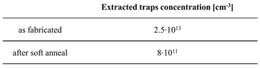
The simulations were compared with the experimental data through an automated routine that minimizes the error between the simulated and measured impedance spectra. This procedure enabled the extraction of interface trap concentrations for both the as fabricated and annealed device. The obtained values are summarized in Table 2. Nyquist plots obtained with the found concentrations are compared to the experimental impedance spectra in Figure 11 for a VDC = 0 V and in Figure 12 for a VDC = 0.2 V. To validate the accuracy of the extracted trap concentrations, the corresponding values for the as fabricated and annealed devices were implemented in simulations of the I–V characteristics (indicated by markers in Figure 13). The resulting numerical curves were then compared with the experimentally measured I–V curves (solid lines in Figure 13), demonstrating good agreement. This consistency confirms the reliability of the impedance-based method used to extract interface trap concentrations and highlights the critical role of interfacial defect states in determining device performance.
5. Conclusions
In this paper, an analysis of interface trap effects on impedance spectra of dopant free silicon solar cells has been performed. The experimental dopant free solar cell structure has been fabricated using c-Si solar cells with a-Si:H/MoOx/ITO as front passivating hole-collector and a-Si:H/LiF/Al as rear passivating electron-collector. The experimental data of the mentioned structure before and after soft anneal have been collected. The illuminated I-V curves show that the soft anneal is beneficial, allowing for a higher open circuit voltage. Correspondingly, the experimental impedance spectra show a larger radius in the Nyquist plots compared to the non-annealed structure. To investigate the differences between the impedance data, a numerical model has been built in TCAD environment. In the simulation, it has been found that a distribution of acceptors/donors traps at the p/i interface causes a change in the impedance spectra. More in detail, the Nyquist plots reduce their circumference as the trap concentration increases. The same analysis has been performed considering the traps distribution at the n/i interface revealing no significant differences in the impedance spectra.
The numerical analysis presented in this study successfully replicates the experimental impedance behavior of dopant-free silicon solar cells through detailed TCAD modelling. Incorporating realistic material parameters and physical mechanisms, as well as explicitly accounting for interface trap distributions at the MoOx/a-Si:H junction, the simulations provided a reliable match to the measured impedance spectra. The optimization routine enabled the extraction of interface trap concentrations for both the as fabricated and annealed devices, with values summarized in Table 2. The simulated Nyquist plots, generated using these concentrations, showed strong agreement with experimental data at different bias voltages. Furthermore, the extracted trap parameters were validated by implementing them in current-voltage simulations, which reproduced the experimental I-V characteristics with high accuracy. This correlation confirms the robustness of the impedance-based extraction method and emphasizes the impact of interface quality on overall device performance. Notably, impedance analysis provides access to electronic properties and interfacial phenomena that are not readily observable through standard I-V characteristics alone. As such, this technique offers valuable insights into the performance-limiting mechanisms of dopant-free solar cells and supports the optimization of their contact interfaces for enhanced device efficiency.
These findings demonstrate the effectiveness of impedance spectroscopy as a diagnostic tool for quantifying interface defect states and guiding the optimization of dopant-free contact architectures in silicon photovoltaic devices.
Author Contributions
Conceptualization, I.M., P.D.V, L.L, L.M and S.D.; methodology, I.M., and S.D., validation, I.M., and S.D.; resources, L.L, E.B., I.U., M.D.N., E.S., P.S., L.M., P.D.V., formal analysis, I.M., and S.D., investigation, I.M., and S.D.; data curation, I.M., and S.D.; writing—original draft preparation, I.M., L.L, L.M and S.D.; writing—review and editing, I.M., S.D.; supervision, P.D.V, L.M and S.D.; project administration, S.D and P.D.V.; funding acquisition, S.D and P.D.V. All authors have read and agreed to the published version of the manuscript.
Funding
This research received no external funding.
Data Availability Statement
Dataset available on request from the authors.
Acknowledgments
This work was supported by the Italian Ministry of Environment and Energy Security in the framework of the Operating Agreement with ENEA for Research on the Electric System and of the Project GoPV (CSEAA_00011) for Research on the Electric System.
Conflicts of Interest
The authors declare no conflicts of interest.
Abbreviations
The following abbreviations are used in this manuscript:
| AC | Alternate current |
| Al | Aluminium |
| a-Si:H | Amorphous Silicon |
| c-Si | Crystalline silicon |
| DC | Direct current |
| DUT | Device under test |
| ETL | Electron transport layer |
| HTL | Hole transport layer |
| IS | Impedance spectroscopy |
| ITO | Indium tin oxide |
| LiF | Lithium fluoride |
| MoOx | Molybdenum oxide |
| PECVD | Plasma-enhanced chemical vapor deposition |
| PERC | Passivated emitter and rear cell |
| SHJ | Silicon heterojunction |
| Si | Silicon |
| TCO | Transparent conductive oxide |
References
- Matacena, I., Lancellotti, L., Daliento, S., Alfano, B., De Maria, A., La Ferrara, V., ... & Guerriero, P. (2023). Impedance Spectroscopy of Perovskite Solar Cells With SnO 2 Embedding Graphene Nanoplatelets. IEEE Journal of Photovoltaics. [CrossRef]
- Yadav, P., Pandey, K., Bhatt, V., Kumar, M., & Kim, J. (2017). Critical aspects of impedance spectroscopy in silicon solar cell characterization: A review. Renewable and Sustainable Energy Reviews, 76, 1562-1578. [CrossRef]
- Sacco, A. (2017). Electrochemical impedance spectroscopy: Fundamentals and application in dye-sensitized solar cells. Renewable and Sustainable Energy Reviews, 79, 814-829. [CrossRef]
- Matacena, I., Guerriero, P., Lancellotti, L., Alfano, B., De Maria, A., La Ferrara, V., ... & Daliento, S. (2023). Impedance spectroscopy analysis of perovskite solar cell stability. Energies, 16(13), 4951. [CrossRef]
- Von Hauff, E., & Klotz, D. (2022). Impedance spectroscopy for perovskite solar cells: characterisation, analysis, and diagnosis. Journal of Materials Chemistry C, 10(2), 742-761. [CrossRef]
- Matacena, I., Guerriero, P., Lancellotti, L., Bobeico, E., Lisi, N., Chierchia, R., ... & Daliento, S. (2023). Capacitance–Voltage Investigation of Encapsulated Graphene/Silicon Solar Cells. IEEE Transactions on Electron Devices, 70(8), 4243-4250. [CrossRef]
- Fabregat-Santiago, F., Garcia-Belmonte, G., Mora-Seró, I., & Bisquert, J. (2011). Characterization of nanostructured hybrid and organic solar cells by impedance spectroscopy. Physical chemistry chemical physics, 13(20), 9083-9118. [CrossRef]
- Matacena, Ilaria, et al. “SiC MOSFETs capacitance study.” e-Prime-Advances in Electrical Engineering, Electronics and Energy 5 (2023): 100251. [CrossRef]
- Lancellotti, L., Bobeico, E., Della Noce, M., Veneri, P. D., & Matacena, I. (2018, June). Work function determination of transparent contact for a: Si/c-Si heterojunction solar cells. In 2018 IEEE International Conference on Environment and Electrical Engineering and 2018 IEEE Industrial and Commercial Power Systems Europe (EEEIC/I&CPS Europe) (pp. 1-5). IEEE.
- Lancellotti, L., Lisi, N., Veneri, P. D., Bobeico, E., Matacena, I., & Guerriero, P. (2019, July). Graphene-on-Silicon solar cells with graphite contacts. In 2019 International Conference on Clean Electrical Power (ICCEP) (pp. 199-203). IEEE.
- Gobbo, C., Di Palma, V., Trifiletti, V., Malerba, C., Valentini, M., Matacena, I., ... & Tseberlidis, G. (2023). Effect of the ZnSnO/AZO interface on the charge extraction in Cd-free kesterite solar cells. Energies, 16(10), 4137. [CrossRef]
- Matacena, I., Maresca, L., Riccio, M., Irace, A., Breglio, G., & Daliento, S. (2020, August). Evaluation of Interface Traps Type, Energy Level and Density of SiC MOSFETs by Means of CV Curves TCAD Simulations. In Materials Science Forum (Vol. 1004, pp. 608-613). Trans Tech Publications Ltd.
- Matacena, I., Maresca, L., Riccio, M., Irace, A., Breglio, G., Castellazzi, A., & Daliento, S. (2022, July). SiC/SiO2 interface traps effect on SiC MOSFETs Gate capacitance with biased Drain. In 2022 IEEE International Symposium on the Physical and Failure Analysis of Integrated Circuits (IPFA) (pp. 1-5). IEEE.
- Matacena, I. (2019, July). Equivalent circuit extraction procedure from Nyquist plots for graphene-silicon solar cells. In 2019 15th Conference on Ph. D Research in Microelectronics and Electronics (PRIME) (pp. 273-276). IEEE.
- Blakers A. Development of the PERC solar cell. IEEE J Photovolt.2019;9(3):629-635. [CrossRef]
- S. De Wolf, A. Descoeudres, Z.C. Holman, C. Ballif, 2012, , High-efficiency Silicon Heterojunction Solar Cells: A Review 27–24. [CrossRef]
- M. Green at al, Solar Cell Efficiency Tables (Version 65), Progress in Photovoltaics: Researc and Applications, 2025; 33:3–15. [CrossRef]
- Holman, Z. C. et al. Current losses at the front of silicon heterojunction solar cells. IEEE J. Photovolt. 2, 715 (2012). [CrossRef]
- Fujiwara, H. & Kondo, M. Eects of a-Si:H layer thicknesses on the performance of a-Si:H/c-Si heterojunction solar cells. J. Appl. Phys. 101, 054516 (2007). [CrossRef]
- de Nicolás, S. M., Muñoz, D., Ozanne, A. S., Nguyen, N. & Ribeyron, P. J. Proc. SiliconPV 2011 Conf. 1st Int. Conf. Cryst. Silicon Photovolt. Vol. 8, 226231 (2011).
- Battaglia, C., Yin, X., Zheng, M., Sharp, I. D., Chen, T., McDonnell, S., ... & Javey, A. (2014). Hole selective MoO x contact for silicon solar cells. Nano letters, 14(2), 967-971. [CrossRef]
- Gerling, L. G., Mahato, S., Morales-Vilches, A., Masmitja, G., Ortega, P., Voz, C., ... & Puigdollers, J. (2016). Transition metal oxides as hole-selective contacts in silicon heterojunctions solar cells. Solar Energy Materials and Solar Cells, 145, 109-115. [CrossRef]
- Bullock, J., Hettick, M., Geissbühler, J., Ong, A. J., Allen, T., Sutter-Fella, C. M., ... & Javey, A. (2016). Efficient silicon solar cells with dopant-free asymmetric heterocontacts. Nature Energy, 1(3), 1-7. [CrossRef]
- Wan, Y., Samundsett, C., Bullock, J., Allen, T., Hettick, M., Yan, D., ... & Cuevas, A. (2016). Magnesium fluoride electron-selective contacts for crystalline silicon solar cells. ACS applied materials & interfaces, 8(23), 14671-14677. [CrossRef]
- Xu, X., Bullock, J., Schelhas, L. T., Stutz, E. Z., Fonseca, J. J., Hettick, M., ... & Ager, J. W. (2016). Chemical bath deposition of p-type transparent, highly conducting (CuS) x:(ZnS) 1–x nanocomposite thin films and fabrication of Si heterojunction solar cells. Nano letters, 16(3), 1925-1932. [CrossRef]
- Zielke, D., Pazidis, A., Werner, F., & Schmidt, J. (2014). Organic-silicon heterojunction solar cells on n-type silicon wafers: The BackPEDOT concept. Solar Energy Materials and Solar Cells, 131, 110-116. [CrossRef]
- Nagamatsu, K. A., Avasthi, S., Sahasrabudhe, G., Man, G., Jhaveri, J., Berg, A. H., ... & Sturm, J. C. (2015). Titanium dioxide/silicon hole-blocking selective contact to enable double-heterojunction crystalline silicon-based solar cell. Applied physics letters, 106(12). [CrossRef]
- Bullock, J., Hettick, M., Geissbühler, J., Ong, A. J., Allen, T., Sutter-Fella, C. M., ... & Javey, A. (2016). Efficient silicon solar cells with dopant-free asymmetric heterocontacts. Nature Energy, 1(3), 1-7. [CrossRef]
- L. Cao, P. Procel, A. Alca˜niz, J. Yan, F. Tichelaar, E. ¨Ozkol, Y. Zhao, C. Han, G. Yang, Z. Yao, M. Zeman, R. Santbergen, L. Mazzarella, O. Isabella, 2023.
- Prog. Photovolt Res Appl. 2023;31:1245–1254; Nano Energy 131 (2024) 110282.
- Bobeico, E., Mercaldo, L. V., Morvillo, P., Usatii, I., Della Noce, M., Lancellotti, L., ... & Delli Veneri, P. (2020). Evaporated MoO x as general back-side hole collector for solar cells. Coatings, 10(8), 763. [CrossRef]
- B. Demaurex, J.P. Seif, S. Smit, B. Macco, W.M.M. Kessels, J. Geissbühler, S. De Wolf, C. Ballif, Atomic-layer-deposited transparent electrodes for silicon heterojunction solar cells, IEEE J. Photovolt. 4 (2014) 1387–1396. [CrossRef]
- Mercaldo et al. Solar Energy Materials and Solar Cells 169 (2017) 113–121.
- Essig et al., Sol. RRL 2018, 2, 1700227.
- Dev, Synopsys. “Simulation, TCAD Sentaurus Manual.”.
- Mehmood, H., Nasser, H., Tauqeer, T., & Turan, R. (2019). Simulation of silicon heterostructure solar cell featuring dopant-free carrier-selective molybdenum oxide and titanium oxide contacts. Renewable Energy, 143, 359-367. [CrossRef]
- Vijayan, R. A., Masilamani, S., Kailasam, S., Shivam, K., Deenadhayalan, B., & Varadharajaperumal, M. (2019). Study of surface passivation and charge transport barriers in DASH solar cell. IEEE Journal of Photovoltaics, 9(5), 1208-1216. [CrossRef]
- Khokhar, M. Q., Hussain, S. Q., Pham, D. P., Lee, S., Park, H., Kim, Y., ... & Yi, J. (2020). Simulation of silicon heterojunction solar cells for high efficiency with lithium fluoride electron carrier selective layer. Energies, 13(7), 1635. [CrossRef]
- Liu, J., Chen, W., & Feng, X. (2018). Numerical simulation of ultra-thin CdTe solar cells with a buffer layer of MoOx in the backwall configuration. Chinese Journal of Physics, 56(5), 1826-1833. [CrossRef]
- Khokhar, M. Q., Hussain, S. Q., Pham, D. P., Alzaid, M., Razaq, A., Sultana, I., ... & Yi, J. (2021). Role of electron carrier selective contact layer of lithium fluoride films with wide bandgap and low work function for silicon heterojunction solar cells. Materials Science in Semiconductor Processing, 134, 105982. [CrossRef]
Figure 1.
Schematic of the solar cells structure studied in this work.
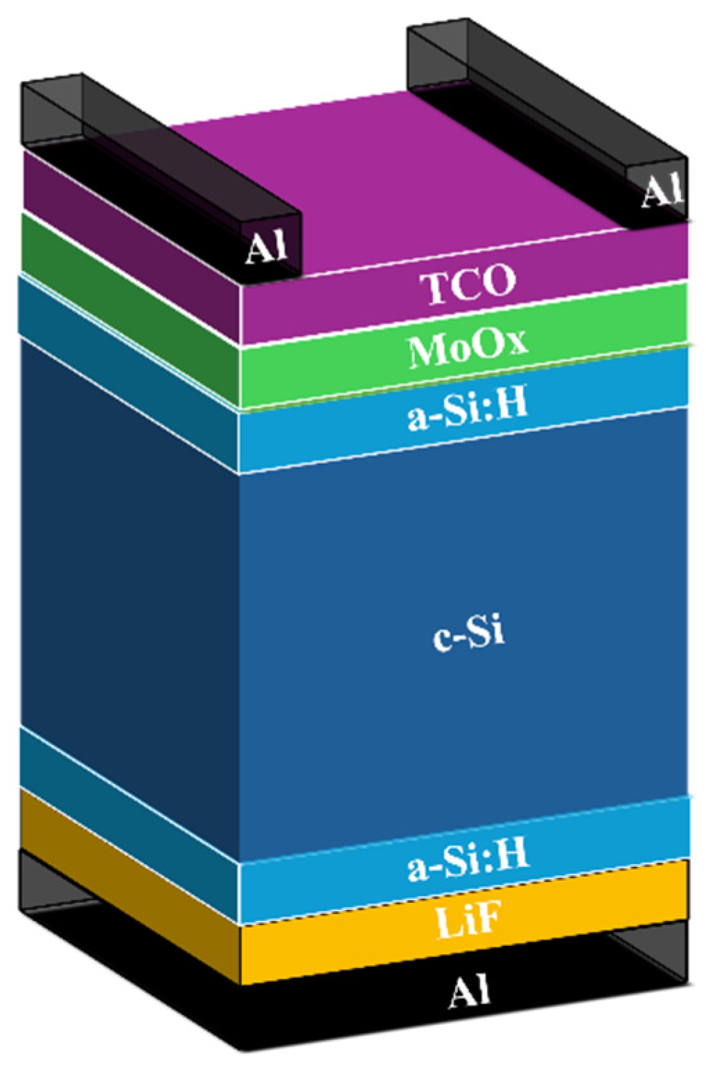
Figure 2.
Current density versus voltage characteristics under light conditions of device as fabricated, blue curve, and after the soft anneal, red curve. The inset reports the open circuit voltage obtained for both cases.
Figure 2.
Current density versus voltage characteristics under light conditions of device as fabricated, blue curve, and after the soft anneal, red curve. The inset reports the open circuit voltage obtained for both cases.

Figure 3.
3D Nyquist plots of the considered structure before and after annealing obtained for VDC = 0 V. The blue curve represents the structure before annealing while the red line has been obtained after the mentioned treatment.
Figure 3.
3D Nyquist plots of the considered structure before and after annealing obtained for VDC = 0 V. The blue curve represents the structure before annealing while the red line has been obtained after the mentioned treatment.
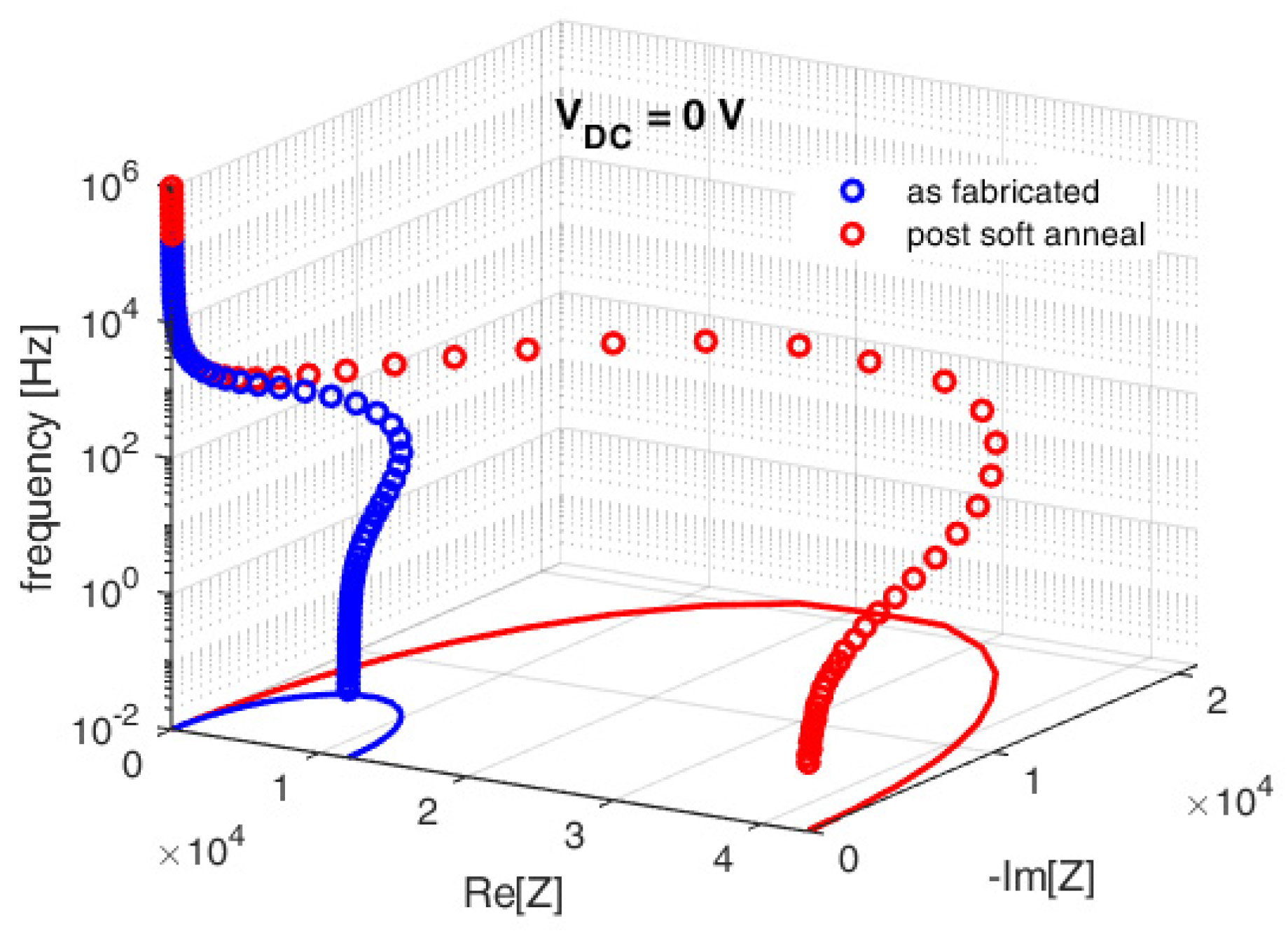
Figure 4.
3D Nyquist plots of the considered structure before and after annealing obtained for VDC = 0.2 V. The blue curve represents the structure before annealing while the red line has been obtained after the mentioned treatment.
Figure 4.
3D Nyquist plots of the considered structure before and after annealing obtained for VDC = 0.2 V. The blue curve represents the structure before annealing while the red line has been obtained after the mentioned treatment.
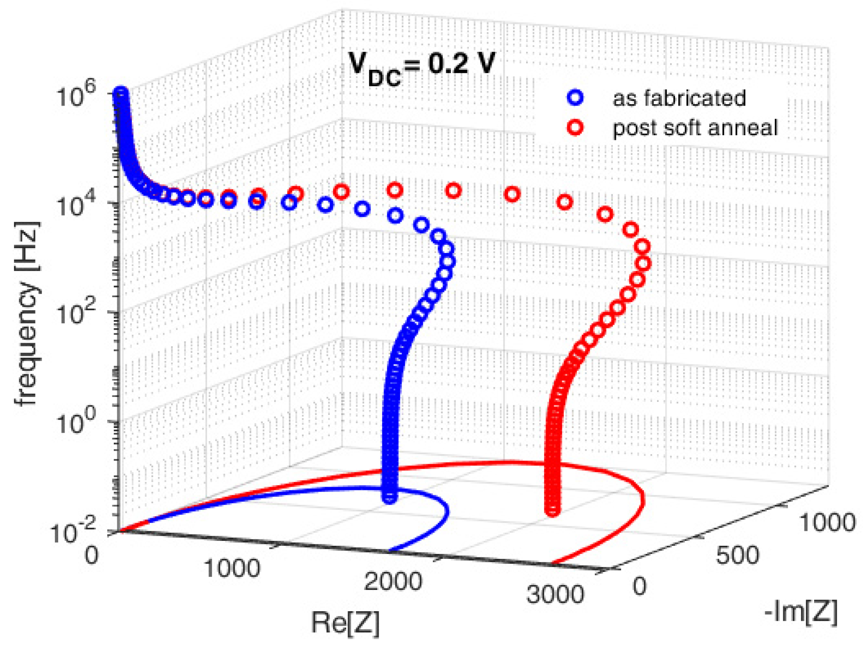
Figure 5.
3D Nyquist plots of the considered structure before and after annealing obtained for VDC = 0.4 V. The blue curve represents the structure before annealing while the red line has been obtained after the mentioned treatment.
Figure 5.
3D Nyquist plots of the considered structure before and after annealing obtained for VDC = 0.4 V. The blue curve represents the structure before annealing while the red line has been obtained after the mentioned treatment.
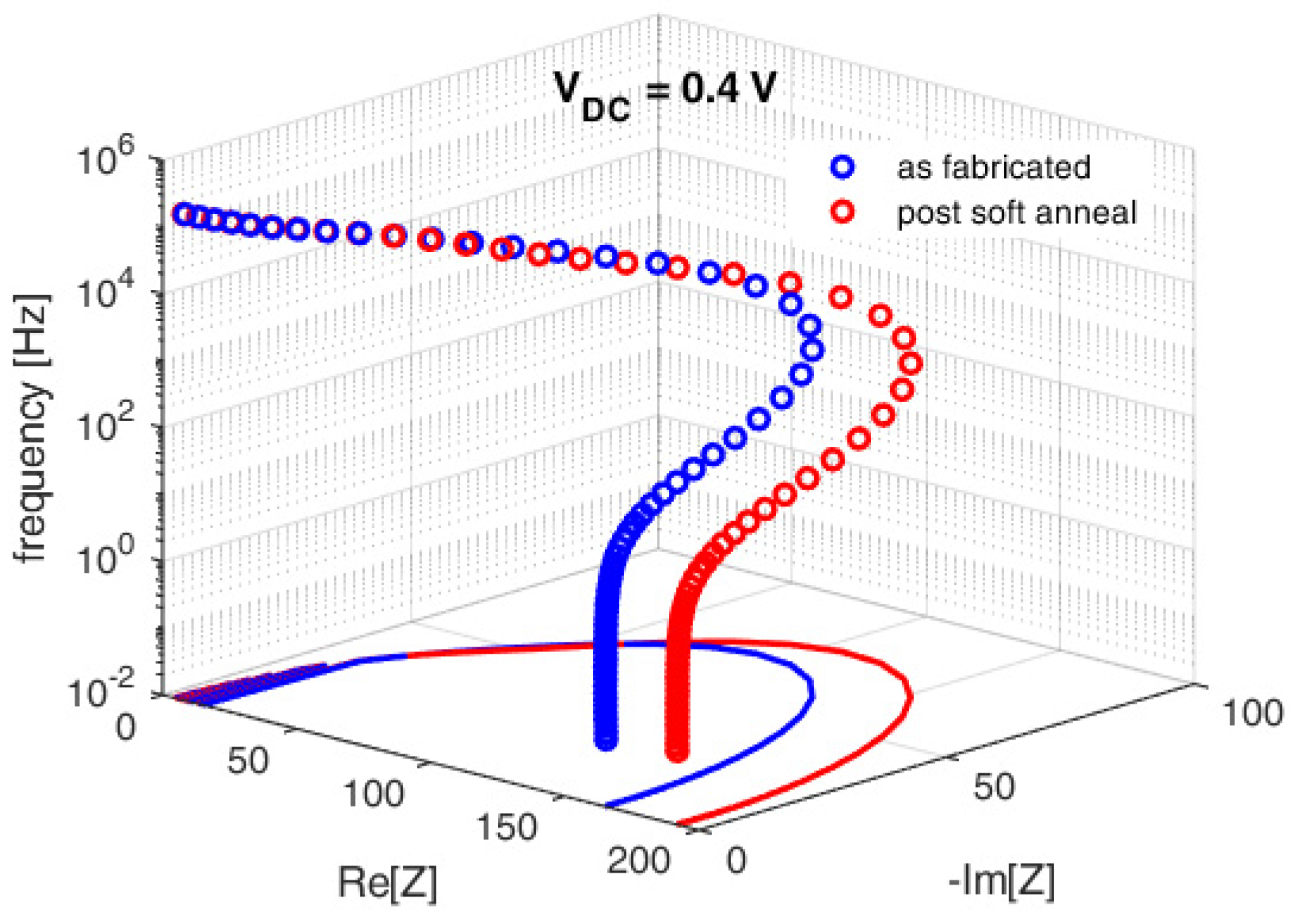
Figure 6.
Sketch of the test structure described in Sentaurus TCAD.
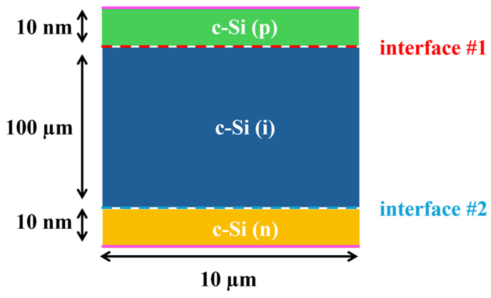
Figure 7.
Schematic implemented in Sentaurus TCAD to obtain Nyquist plots.
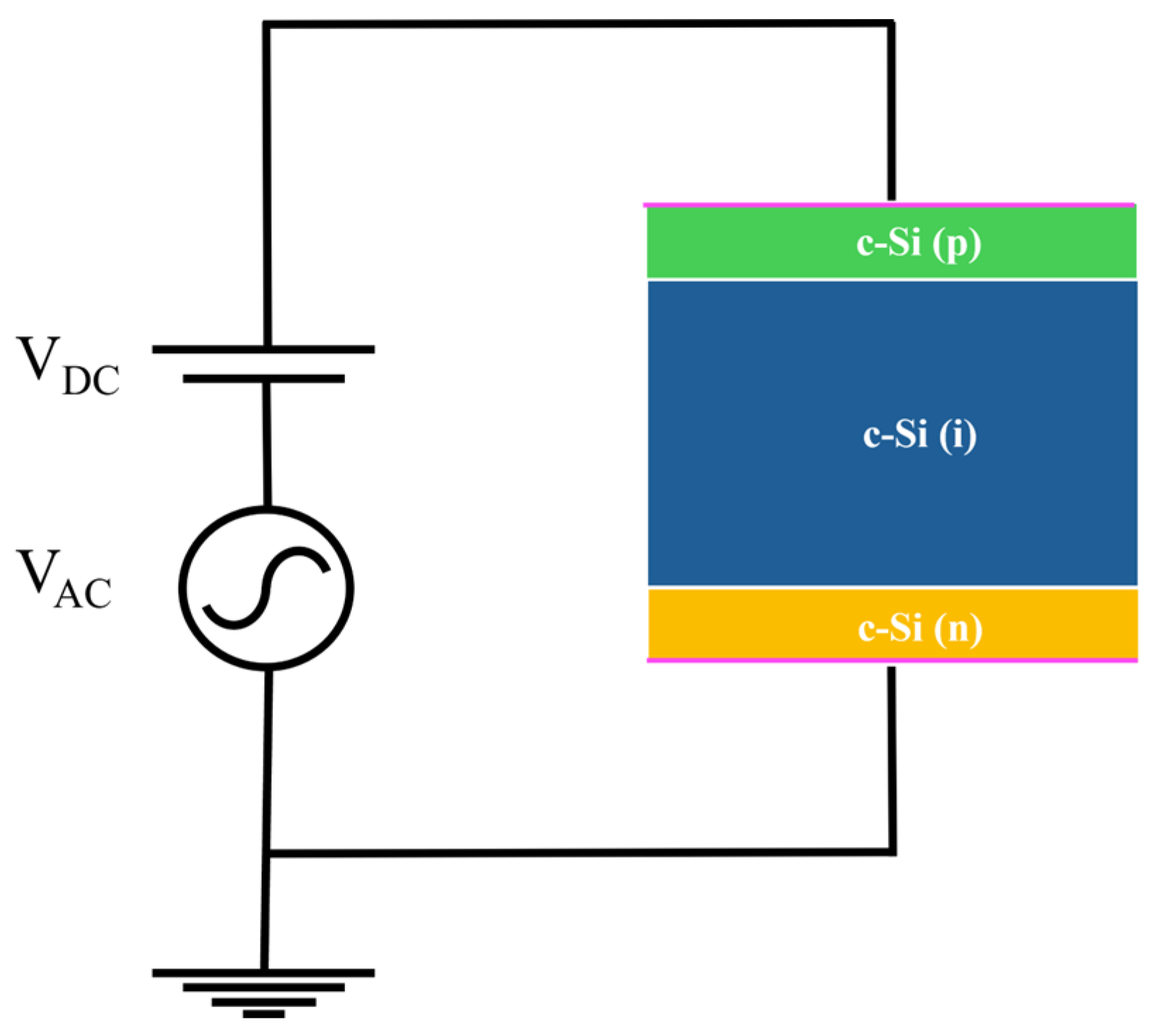
Figure 8.
Numerical Nyquist plot obtained at VDC = 0.2 V from structure of Figure 6 in the case no interface traps are considered, markers, and in the case acceptors traps are considered at interface #1. The concentrations considered are the following: Cit1 = 1∙1011 cm-2, Cit2 = 1∙1012 cm-2, Cit3 = 5∙1012 cm-2, Cit4 = 1∙1013 cm-2. The uniform trap band has a ETW = 0.2 eV, while the capture cross section for electron, σn, is equal to the hole capture cross section, σp = 1∙1016 cm2.
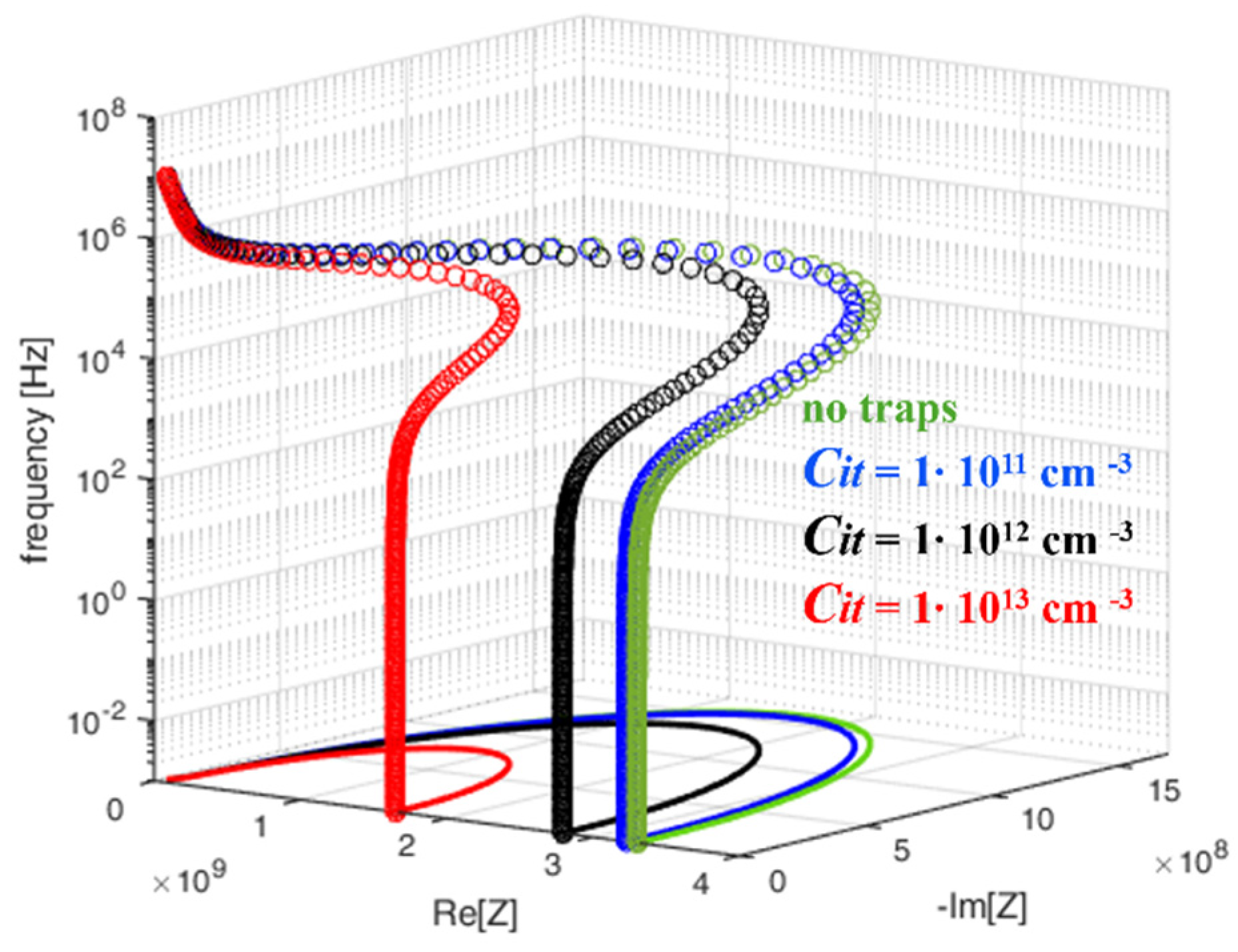
Figure 9.
Numerical Nyquist plot obtained at VDC = 0.2 V from structure of Figure 6 in the case no interface traps are considered, green markers, and in the case acceptors like traps are considered at the interface #2. The concentrations considered are the following: Cit1 = 1∙1011 cm-2, Cit2 = 1∙1012 cm-2, Cit3 = 5∙1012 cm-2, Cit4 = 1∙1013 cm-2.
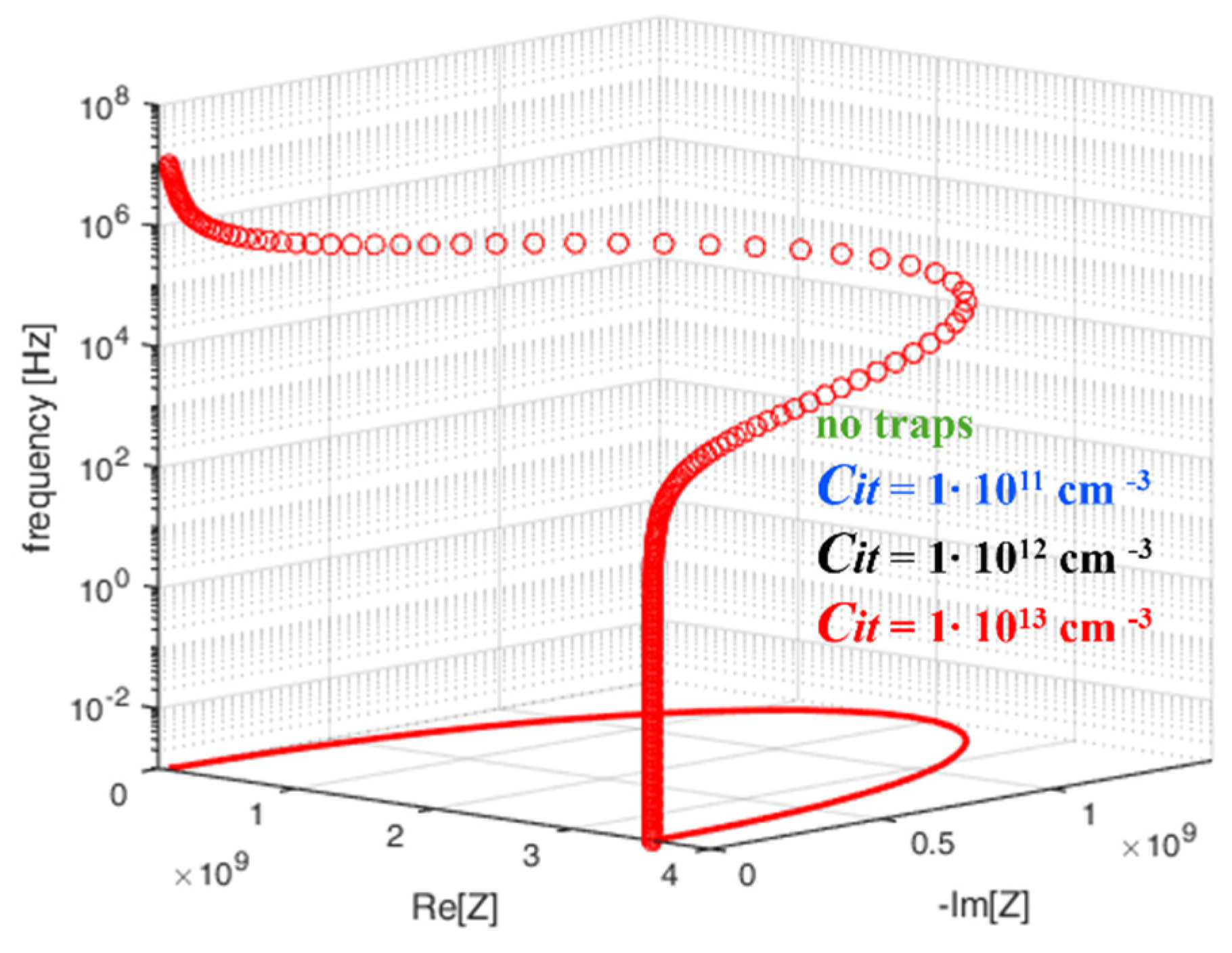
Figure 10.
Sketch of the experimental structure described in Sentaurus TCAD.
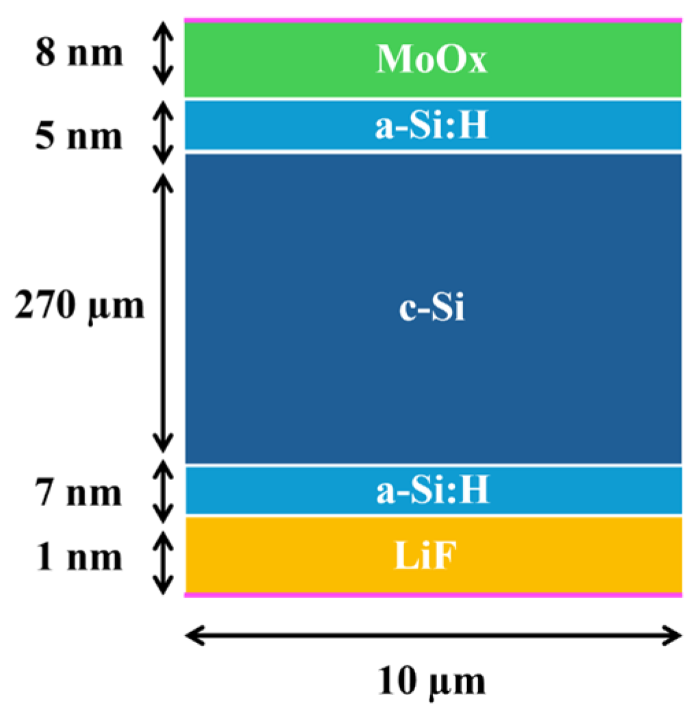
Figure 11.
Nyquist plots obtained at VDC = 0 V from numerical analysis as fabricated (blue markers) and after (red markers) compared to experimental results from structure as fabricated (blue line) and after (red line).
Figure 11.
Nyquist plots obtained at VDC = 0 V from numerical analysis as fabricated (blue markers) and after (red markers) compared to experimental results from structure as fabricated (blue line) and after (red line).
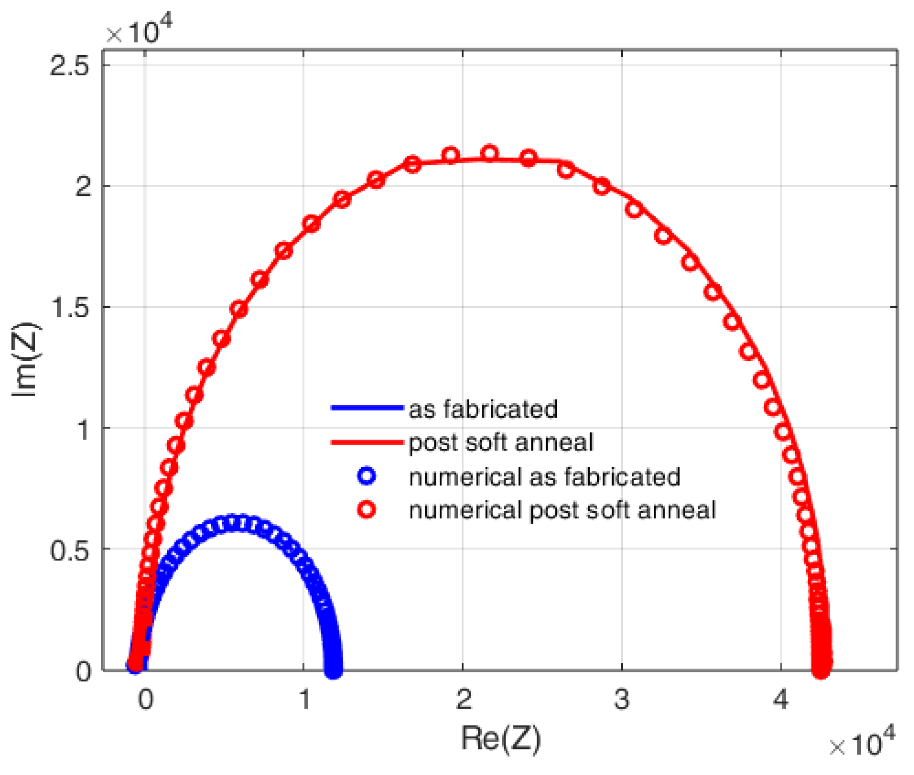
Figure 12.
Nyquist plots obtained at VDC = 0.2 V from numerical analysis as fabricated (blue markers) and after (red markers) compared to experimental results from structure as fabricated (blue line) and after (red line).
Figure 12.
Nyquist plots obtained at VDC = 0.2 V from numerical analysis as fabricated (blue markers) and after (red markers) compared to experimental results from structure as fabricated (blue line) and after (red line).

Figure 13.
Numerical current density versus voltage characteristics under light conditions of device as fabricated (blue markers) and after (red markers) compared to experimental results as fabricated (blue line) and after (red line).
Figure 13.
Numerical current density versus voltage characteristics under light conditions of device as fabricated (blue markers) and after (red markers) compared to experimental results as fabricated (blue line) and after (red line).
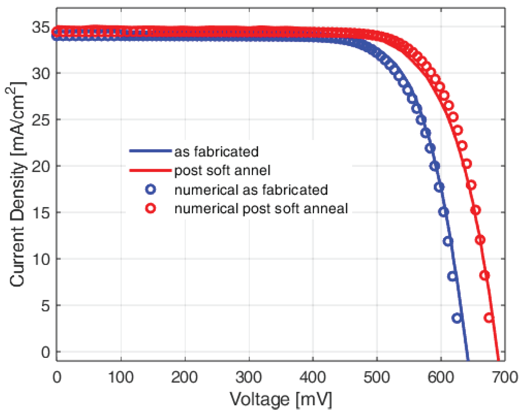

Table 1.
Physical properties used in TCAD environment.
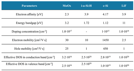 |
Table 2.
Extracted MoOx/a-Si:H interface traps concentrations.
 |
Disclaimer/Publisher’s Note: The statements, opinions and data contained in all publications are solely those of the individual author(s) and contributor(s) and not of MDPI and/or the editor(s). MDPI and/or the editor(s) disclaim responsibility for any injury to people or property resulting from any ideas, methods, instructions or products referred to in the content. |
© 2025 by the authors. Licensee MDPI, Basel, Switzerland. This article is an open access article distributed under the terms and conditions of the Creative Commons Attribution (CC BY) license (http://creativecommons.org/licenses/by/4.0/).
Copyright: This open access article is published under a Creative Commons CC BY 4.0 license, which permit the free download, distribution, and reuse, provided that the author and preprint are cited in any reuse.


