
Submitted:
11 July 2025
Posted:
14 July 2025
You are already at the latest version
Abstract
More and more chemosensors and biosensors are turning to electronic transistors, as ideal transducers, precise in current response, miniaturized in size and capable of providing sub-picomolar detection limits. Among these devices, ISFET transistors - Ion Sensitive Field Effect Transistors, have the capacity of integrating ion-sensitive layers together with field effect transistors of ultimate generations. Recent studies have indicated that nanoporous materials deposited or grown within the transistor gate space offer a dual advantage - a favorable environment for an optimal capture of liquid state receptors through capillary effects, but also of direct anchoring of these nanoporous structures on Si-wafer. This article aims to review the constructive evolutions of ISFET transistors along with some newer nano-wire devices, along with their co-integration techniques with nanoporous materials, beneficial in the optimization of many chemosensors, but of enzymatic biosensors, in particular.
Keywords:
nanoporous layers
; chemosensors
; ISFET
; silicon nano-wires
; sensitive film
1. Introduction
In the last five years, electronics has proposed the smallest Field-Effect Transistors (FETs) ever manufactured, generating 2 nm technology [1]. Their miniaturization in the coming years will be limited by the dimension of one atomic layer, up to 0.2 .... 0.5 nm [2]. For this reason, the roadmap of semiconductor devices has also been directed towards integrated sensors, especially chemosensor applications [2,3]. From the transducer point of view, the next biosensor families belong to the bio-receptors integrated near nano-transistors [3,4,5], sometimes Artificial Intelligence (AI) assisted [6], to produce different kinds of Biosensors-Field Effect Transistors (BioFET), [5,6,7,8].
On the other hand, chemoscience pays attention to those sensors that are technologically compatible with micro- and nano-electronic devices, [9]. What must be emphasized from the beginning concerns these smallest transistors, with dimensions of 1 .... 20 nm, which are mainly used for the manufacture of memories and computer processors, where the fight for supremacy in processing speed and packaging density is the strongest [10]. But nowadays analog electronics, or electronics for interfacing with real phenomena from the environment, such as the field of transducers for sensors, the 2 nm technology is not in use. More relaxed and very well-experienced technological nodes are used, such as the 150 nm Metal Oxide Semiconductor Field Effect Transistor (MOSFET) [11], or 300 nm for Ion Sensitive Field Effect Transistor (ISFET) sensor based, [12] or more than 300 nm for organic transistors [13,14].
A sub-field of chemosensors concerns the feeding tubes, consisting in capillaries that supply tiny amounts of liquids to lab-on-a-chip platforms [15]. MEMS (Micro-Electro-Mechanical System) integration techniques are often borrowed from micro-nano-electronics in these scopes, [16,17]. Another direction related to sensors concerns those methods able to grow nano-porous layers directly on glossy surfaces of Si, SiO2 or Si3N4 frequently encountered in the usual transistor’s technology [18,19,20,21]. The pores size is technological controlled, so that they are able to bind bio-receptors in liquid phase in the above layers, during the immobilization technological steps. If Ion Sensitive Electrodes (ISE) represent the receptors and FETs represent the transducers, then the resulting sensors work as an ISFET Transistor, [22].
Therefore, a main goal of this review is to find the optimum way of the sensitive layers integration on the top of the silicon-wafer, in the device proximity [23] or on a separate extended gate [24,25], as an Extended Gate Field Effect Transistor (EGFET), [26,27,28,29], aspects that will be approached in depth in this paper, too.
Another important technological aspect of this review consists of defining an optimal enzyme immobilization technology, using nanoporous materials [30,31], and the theory of viscous liquids captured by capillarity [32], with applications in biosensors [33], even paper-based devices [34]. In particular, the Enzyme-FETs fabrication requires these technological processes of bio-catalysts immobilization. Liquid enzyme solutions mixed with high concentrations of cross-linkers can lead sometimes to proper immobilization, but other-times accompanied by enzyme activity alleviation [35] and even poor adherence [36]. The first generations of biosensors used enzyme immobilization in gels [37,38], but later they switched their capture on nano-porous or nano-structured materials [39,40]. Therefore, a middle resolution would result from a combination between chemical immobilization methods and capillary-based physical methods.
A final topic of this paper concerns the finding of the optimal location for anchoring nano-porous materials used in chemosensors. The ideal location would be the proximity of the conduction channel of the transistor, to influence as sensitively as possible the current through this device. Some authors have proposed an optimum location just above the gate insulator [41,42]. Technological inconsistencies immediately arise: if we intend to use nano-transistors with extremely small gate areas, then the amount of enzyme that can be immobilized becomes negligibly small, which reduces the sensitivity of the sensor. In addition, during measurements with liquid droplets above the sensitive layer, contamination of the gate insulator with ions by the flat-band effect or accidental gate-source current leakage via liquid drop may occur [43]. Moving the entire sensitive area to the so-called Extended Gate, advantages such as electrical isolation successfully occur, but accompanied by disadvantages, such as poor influence of the ion charges generated in the extended gate area on the current through a distant channel [44]. However, a general opinion suggests attaching the sensitive layers just above the gate space [45]. Alternative transistors with Solution Gates FETs (SGFET) in contact with the liquid analyte solution would be a possibility for integration of a solid-state transducer with a liquid analyte solution [46,47]. However evaporation phenomena and possible secondary reactions at an electrode, make the SGFETs an imprecise and more degradable device than a silicon based ISFETs. ISFET transistors have accumulated over 50 years of experience [48] being the most resilient over years of use.
However, the discovery of a technology able to directly capture nanomaterials near low size transistors, technology which is also capable of immobilizing enzymes or other liquid bioreceptors, being also compatible with standard CMOS or ISFET technologies, is still a challenge [49,50]. This is the further argument for which this review is carried out, finally emphasizing the possible development directions for the next future.
2. ISFET Work Principle and Technological Challenges
2.1. From ISFET Theory to Materials Motivation
Bergvelt, the ISFET’s father, describes the evolution of this transistor after thirty years of existence [51], in conjunction with its sensitive layers integration. ISFET is essentially a Metal-Oxide Semiconductor Field Effect Transistor (MOSFET) [52], biasing the gate by a separate connection to a standard electrode placed in an aqueous electrolyte in connection with the Gate oxides, Figure 1.
The threshold voltage of an ISFET depends on the concentration of ions in the solution after a model reported in [8], corrected by an α parameter [53]:
where, V0 is the standard electrode potential, VFB is the flat-band voltage of the transistor, ϕF is the Fermi potential in semiconductor, kT/q is the thermal voltage, c is the analyte concentration, and α is a sensitivity factor depending on the ability of the oxide surface to supply or to acquire protons by the capacitance of the double-layer, while ΔV is the last term from eq. (1). The α parameter is ideally 1 for a maximum sensitivity, or it is subunitary for realistic compounds such as SiO2, Si3N4, Al2O3, Ta2O5, deposited over the usual gate oxide of a transistor [51].
The last term from eq. (1) was extracted from experimental ISFETs for each previous oxides [51] and computed for HfO2 oxide, after the model depicted in [8], considering as electrolyte NaCl (aq. solution at pH=5.8), Figure 2.
The α parameter depends on the capacitance of the double-layer at the electrolyte/oxide interface CD, and the surface capacity, Cs [53]:
The Cs value can be expressed in terms of the acidic or basic equilibrium constants of the related surface reactions [8,51]. For the above oxides, the α parameter takes sub-unitary values that is equivalent with sub-Nernstian sensitivities. Hence, ISFET transistors can use not only conductive materials ISE (Ion Sensitive Electrodes) as sensitive elements for the ions detection, but also different gate oxides that translate analyte concentration variations through the buffer capacity of the insulator surface.
2.2. ISFET Particular Technology
One dissimilarity between the ISFET and the MOSFET, besides some different gate oxide stacks, is that the S, D metal contacts are laterally spaced from the gate electrode. This requires particular long lateral S, D diffusions that extend from the gate oxides far toward the drain metallic contact. This effect is presented by the technology simulation, in Figure 3.a. These diffusions produce large series resistances that will lead to a decrease of the transconductance gm of a ISFET, versus gm of a MOSFET, [52], diminishing the device sensitivity.
Another specific technological process of the needle ISFET transistors, usable in vivo, is silicon etching, firstly described in 1978 by Esashi et al [54]. Later, the etching process was transferred to silicon on sapphire (SOS) wafer that is a particular silicon on insulator (SOI) technique [55]. The technological advantage of the buried insulator usage, as an excellent etching stop layer for silicon, propagates till nowadays [56]. The further SOI advantage is fulfilled: a complete isolate chip occurs, because the source and drain metallizations are placed on the top side, while the back gate is placed on the bottom side of the wafer [56]. To emphasize these particularities, an example of SOI structure is presented in Figure 3.b. The current vectors arise at the bottom of the Si-p film, if electrons are driven by the back-gate. Another technological incompatibility arises: a back gate integration with ion sensitive material on the top side of any Extended Gate structure becomes impossible, [24,25,26,27,28,29].
However, a full isolation of a Si-chip is expensive for a typical disposable sensor. If all terminals are on the same side of the chip, usually as top electrodes, there still exists another drawback of ISFET - its short-term stability. When it is in touch with aqueous ionic solutions, from the test samples, some corrosion processes occur near the gate electrode, reducing its lifetime [57]. To eliminate this effect, the ion-sensitive part was extended outside the electronic chip, as a longer electrode. This new device architecture is known as Extended-Gate-Field Effect Transistor (EGFET) [25,26,27,28,29] and was recently optimized [58,59]. The extended gate is essentially an elongation of the work electrode on the same chip, but outside of the electronic area. In this way, only the extended gate is in contact with the tested liquid, while the FET part rests completely dry.
3. Nano-Structured Oxides Used for Sensitive Layer Integration
3.1. Porous Si on Si-Wafer
It is expected that the materials most compatible with Si technology would be these suitable to be grown, deposited or converted directly onto the Si wafer. Therefore, among the first nanostructured materials to be directly anchored to Si was porous Si (PS). A very accurate study was performed by Hoover Tiffany on the technology of converting Si into porous Si with the pores measured distribution of 67 µm in the center of the wafer and 102 µm on the edges, with a pore width of 1.6 µm, [60]. Other authors reported the porous silicon manufacturing by electrochemical anodization of the top mono-crystalline Silicon surface, by electrolyte of hydrofluoric acid (HF) in Di-Methyl-Formamide (DMF), in order to serve to photovoltaic sensors [61]. The pores diameter took from a few nano-meters to a few microns, according to the silicon wafer properties and electrolyte formula, [61].
Further improvements were more recently described within some optimized technologies [62]. Porous silicon was prepared by electrochemical anodization of a monocrystalline Si-p-type wafer, <100> crystalline orientation. Macro-porous silicon was fabricated for the electrolyte composed by Di-Methyl-Sulfoxide (DMSO) combined with HF 45% at the volume ratio of 10:46 and a current density was 8 mA/ cm2. Meso-porous silicon was fabricated for an aqueous–alcoholic electrolyte composed by isopropanol, HF 45%, and deionized water, at a volume ratio of 1:1:3 and a current density was 30 mA/ cm2, 60 mA/ cm2, and 100 mA/ cm2 for a time of 20 sec, 22 sec, and 20 sec, respectively, Figure 4. Different pores size between 2 nm to 50 nm resulted.
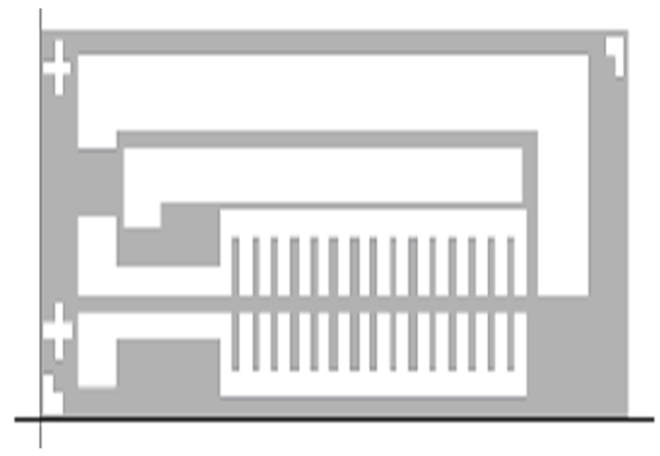
For the application of PS in the construction of gas sensors, a crystalline Si-substrate <100> orientation p- or n-type was the start wafer to produce PS with 45% porosity. The PS structures were fabricated in a Teflon electrochemical cell by hydrofluoric acid (HF) (48%) and almost pure ethanol (EtOH) (99.98%) as electrolyte, under a current density of 13.6 mA/cm2 for p-type and 10 mA/cm2 for n-type. The anodization time ranged between 64 - 825 sec, to achieve the proposed layers thicknesses between 1 to 10 μm [63]. For the sensor fabrication, Al electrodes were deposited by a geometric predefined pattern, of two electrodes. The electrodes contained two concentric rings of 1 mm width, and a trace connector of 1 mm width. Figure 5a shows the sizes of the geometric shape, while Figure 5b shows a photograph of the sensor with deposited aluminum on the Si-porous regions.
Few years later, metal-assisted chemical etching (MACE) method was applied to PS film on silicon wafer, making it able to be transferred to another substrate [64]. Few windows were opened on a Si-wafer covered by thin silver film by lift-off, that was subsequently immersed in an etch MACE cell, using a mixture of HF, H2O2, and deionized DI water. After the samples were completely etched and dried in the nitrogen environment, the horizontal cracks occurred; consequently, the PS film suffered self-peeling from the Si substrate. The Si-pores size was dependent on the ratio R of HF to H2O2 etchant: R = 5:5, 6:4, 7:3, 8:2, and 9:1, for 30 min, shown below through SEM imaging, Figure 6. The great advantage of this method is to define a robust technology of vertical transfer for large-area PS films onto inorganic and rather organic substrates.
In 2024, a step forward in the PS development was the transition to porous Silicon-nanotubes (PSi-NT), [65]. The synthesis of gold nanoparticles (Au-NPs) functionalized with 4-Merca-Ptophenyl-Boronic Acid (MPBA) on porous Si-nanotubes was possible using nanowires template initiated from ZnO seeds deposited on Si-wafers [65]. Finally, the ZnO was removed in NH4Cl at 500 °C for 120 minutes, using a helium environment. The accomplished typical nanotubes morphology of the processed PSi-NTs is demonstrated by some TEM images, Figure 7a. Then, the PSi-NTs surface is functionalized with 3-aminopropyltriethoxysilane (APTES), acting as a reducing agent. APTES also facilitates the Au-NPs synthesis, followed by the incubation of the Au-precursor solution. Different TEM images of the PSi-NTs structures are presented in Figure 7b-e, for Au-NPs uniform distribution. Figure 7f indicates the size distribution of the Au-NPs. Applications are still valid in glucose biosensor [65] or lithium storage batteries [66]. Ultimate developments in PS based biosensors show PS films able to immobilize amino-terminated anti-LF aptamers [67], for detection of some protein biomarkers, like lactoferrin (LF) [68]. The optimal pore width was 50 nm, being accomplished at a current density of 375 mA/cm2 during 10 - 35 seconds of etching [67].
3.2. Porous Al2O3 on Si-Wafer
One of the pioneering articles, in the field of nanostructured Al2O3 anchoring directly on Si wafer, was reported by the co-authors of this article since 2010 [21]. That proposed multilayer structure Si/SiO2/Si3N4/Al2O3 successfully entrapped a glucoseoxidase (GOX) enzyme within the work electrode. The device works as a glucose biosensor. It was designed as 4 electrodes electrochemical cell, although integrated in Si, but not transistor based. The mono-crystalline form of Al2O3 is known as sapphire.
Figure 8.
Four electrodes used in a glucose biosensor composed by 4 integrated electrodes in Si, where porous Al2O3 helps to GOX immobilization. (redrawn with Springer permission from [21]).
Figure 8.
Four electrodes used in a glucose biosensor composed by 4 integrated electrodes in Si, where porous Al2O3 helps to GOX immobilization. (redrawn with Springer permission from [21]).
Some experimental tests occurred on discrete structures of porous Al2O3 anchored in Si-wafer, still in the absence of a transistors co-integration. The Al film was deposited on a Si-wafer over the previous multilayer structure Si/SiO2/Si3N4, under vacuum conditions at a low deposition rate, with a thickness between 80 and 100nm . This process resulted in the formation of γ-type catalytic Al₂O₃. Figure 9a presents a SEM image of the porous Al2O3 synthesized layer, while Figure 9b shows the experimental current-time dependence during the Al film conversion into porous Al2O3 by anodization at a constant voltage 80 V, in diverse aqueous electrolytes: 1 - (HCOO)2, 2 - (H3PO4), 3 - (HCOO )2 : H3PO4, [69].
The anodic γ-type aluminum oxide offers two key advantages for chemosensors and biosensors: its high adsorptive capacity facilitates effective immobilization of enzyme solutions, and its favorable catalytic properties support the electro-oxidation of certain organic compounds.
Only relatively recent, some Field Effect Transistor FET based biosensors integrated Al2O3 [24] on MoS2 semiconductor and bioreceptor elements [70]. Despite achieving a very low detection limit for the prostate specific antigen (PSA) analyte, (LOD of 1 fg/ml), the use of atomic layer deposition (ALD) technology, multiple functionalization and the use of antigen receptors make it an expensive sensor. On the other hand, the exposure to moisture led to the hydration of aluminum oxide, demonstrating a rapid aging process. This phenomenon was observed in a sapphire gate ISFET [71]. A recent review paper on the ISFET [72] evolution stated that an optimized process use Al2O3 sensing film deposition, configured by the lift-off technology to laterally define this sensing layer.
To improve the adsorbent properties of the porous oxide, in 2025 some authors reported a novel transistor with 10 nm Al2O3 layer on a Ga2O3 layer of different thicknesses between 10 nm and 230 nm, exploring the device performances and revealing efficient reliability for those transistor-based biodetectors, with sub-10 nm Ga2O3 thickness, [73]. In general, there has been no particular focus on nanoporous Al2O3 in ISFETs. Looking for a metal biocompatible with living tissues, we find Ti in almost all prostheses [74,75]. Therefore, we will discuss the nano-structured titanium oxide, which is more widely used in the construction of transistor-based biosensors.
3.3. Nano-Structured TiO2 Grown on Si-Wafer
Another oxide material that can be converted by anodizing into a nanoporous or nanostructured material is titanium oxide. Our research group has been using nanostructured TiO2 for enzyme immobilization since 2011 [36]. It was later proven that the defects and cracks that appeared in the enzyme membrane above the TiO2 were not caused by the underlying oxide, but rather by the adopted crosslinking method [76]. A SEM image of the Glucose-oxidase (GOX) enzyme immobilized on a Si-wafer covered by successive layers of Si/SiO2/TiO2/nafion is presented in Figure 10: (a) top view 1 mm scale for the entire wafer covered by enzyme; (b) detail at 0.1 mm scale, revealing cracks and fissures in the enzyme membrane.
It is not at all efficient to purchase TiO2 nanoparticles from which to create a film in liquid or gel states, which is then deposited on a Si wafer, because the adhesion of such a layer is poor. Instead, it is much more efficient to deposit Titan directly on a Si-wafer, even if sometimes Si is coated with SiO2 or Si3N4, [36]. In all these cases, the Ti surface can then be converted into nanoporous TiO2 or nanostructured TiO2, by anodization in different electrolyte agents, at different electrolysis currents. By adopting such a method, nanoporous TiO2 film, anatase phase, was created, and it is visible at SEM in Figure 11a. In this case, a Ti film of 90 nm thickness was strongly anchored to the substrate by sputtering deposition, on a Si-wafer, p-type, initially doped by 1015 cm-3. The anodization cell had a calomel reference electrode, against which the working electrode and counter electrode were polarized at voltages from 0 to 10 V at a degree of 0.2 ... 0.4 V/s. The electrolyte was aqueous solution of phosphoric acid mixed with oxalic acid, keeping the pH at 6.8÷7.4, by a phosphate buffer [76]. Just after the electrochemical process, the TiO2 layer was amorphous.
After a thermal process at 500°C, the amorphous film gets TiO2 anatase phase, with deep vertical nanotubes, and homogenous nano pores of 10 - 30 nm diameter from a top view, Figure 11.a. A FTIR spectrometer working in the spectral area of 4000 - 370 cm-1, confirms the nanostructured TiO2 presence, Figure 11.b.
In order to immobilize the GOX enzyme above, the cross-linker was changed from nafion to glutaraldehyde, keeping the same nanostructured TiO2 formula. The present spectra were recorded by FTIR, to prove the GOX - glutaraldehyde anchoring on the Si/SiO2/ TiO2 surface, Figure 12.(a). The bands of 1161 cm-1 and 1118 cm-1 are allocated to the stretched Ti-O-C bond, demonstrating a strong anchoring of the GOX cross-linker to substrate. A top uniform film without defects is visible in a SEM view, Figure 12.b.
But nanostructured TiO2 was also studied outside the goal of its enzyme binding. Compared to the case of nanoporous TiO2 annealed at 500 °C from Figure 11.(a), a study of modifying the technological parameters was continued. If the anodizing potential between the electrodes is varied in larger range of 2 – 25 V, keeping 500 °C post-annealing temperature, the surface morphology at the wafer edge presents 40 nm pores, Figure 13a.
If additionally, the post-anodization temperature was increased to 800 °C in the nitrogen atmosphere, the surface morphology proves better uniformity, but similar pores size, Figure 13b.
The nanoporous aspect on the surface should be explained by the nanotube roots, anchored deep inside the oxide, after anodization [77]. Cross-section images of anchored TiO2 nanotubes achieved by anodization in aqueous and glycerol electrolyte at four voltages are presented in Figure 14.
In the case of glycerol as electrolyte, the TiO2 surface is not so rough, it is more superficially anchored, but it is more ordered. These observations lead to the recommendation of aqueous electrolytes for chemo- and bio-sensor applications.
In 2019, a pH sensor, ISFET-based with extended gate area, covered by TiO2 film, was reported [78]. The TiO2 nanostructures were prepared on a fluorine-doped tin oxide as substrate, resulting in so called TiO2 nanoflowers, Figure 15.
The TiO2 precursor solution was premixed with DI water and 36% hydrochloric acid, while titanium(IV) n-butoxide (>99%, 2 mL) was added. The best variant of this sensor measures pH between 2 - 12, with an almost perfect linearity of 99.91%, having a maximum sensitivity of 46 mV/pH, [78], while other nanoporous TiO2 sensors, created in the same period, offered only 19.3 mV/pH sensitivity, [79].
Very recent technological studies describe a 1.5 µm thick titanium layer sputtered onto the SiO2 surface, which was previously grown by thermal processes, [80]. The electrolyte for anodization comprised ethylene glycol with 0.35 wt% NH4F and 1 wt% deionized water. Finally, titanium dioxide nanotubes get a height of 1.2 µm and an inner diameter of the tube of 46 nm, Figure 16. Usual post-anodization thermal treatments were applied at 450℃, to obtain the crystalline state.
4. Other Oxides Used in ISFET and Related-Transistors Construction
Other nanostructured oxides have been used, too, as a sensitive element for ISFET transistors. Here are a few examples. A transistor that avoids the construction of a reference electrode inside the gate space, uses ZnO prepared in sol-gel method to provide a pH sensitive element and offers a sensitivity of 27 mV/pH [81]. However, to be able to immobilize an enzyme within an EGFET biosensor, the oxide must be nanostructured in a so called ZnO nano-array, for the glucose detection [82].
Although created in 2009, a pH ISFET based on vanadium oxide, placed over a hexadecylamine membrane within the gate space, offered superior sensitivity of 38 mV/pH, [83]. However, in 2025, the vanadium oxide combined with graphene oxide (GO) nano-compound is coming back to the attention of glucose biosensor manufacturers, due to its excellent selectivity and sensitivity [84]. In all cases, the synthesis of Mn(V2O6)/GO started from NH4VO3 as a precursor, following a simple and cheap technology.
Another oxide borrowed from modern transistor technology, which is part of the class of high-k dielectrics, was applied in the construction of an EGFET biosensor for blood marker proteins. This is HfO2.
By recent technology, the deposition of thin HfO2 film in the gate space can be performed at a thickness of 20nm by high-power pulsed magnetron sputtering [85]. The performances allow the clinical detection of Parkinson’s biomarkers: a linear response 99.45 % degree, in the detection range of 0.0001–1 ng/mL, a limit of detection of 198 fg/mL and a sensitivity of 12.11 mV/decade.
In order to fabricate a highly sensitive FET-based dopamine biosensor, another oxide plays the role of semiconductor. Consequently, an ultrathin In₂O₃ film of approximately 4 nm thick was fabricated using a sol-gel method, under an inexpensive, large-area spin-coating process [86]. The technology consisted in chemical lift-off lithography, utilizing self-assembled monolayers of alkane-thiols on gold. The ingenious integration technique allowed a bottom-gate, bottom-contact FET coupling with an oxide surface functionalization, capable of immobilizing DNA aptamers, as dopamine receptors [86].
The semiconductor properties of this nanostructured In2O3 material, which can effectively bind certain analytes, have been previously demonstrated, too [87,88]. The transfer characteristics reveal high drain currents stimulated by moderate operation gate voltages, IOFF = 2 x 10-11 A at VGS < 0 V to ION = 70 μA at VGS = 30 V, while VDS = 30 V. The transistor parameters, like ION/IOFF ratio of 107, carriers mobility sub-10cm2/Vs, and threshold voltage around 4 V are in agreement with the transistor size - 35 μm channel width and 15 μm length, plus constituent materials - Au electrodes on SiO2 on Si-wafer, heavily doped Si substrates as back-gate electrode. Also, the output characteristics of this In2O3 transistor shows a saturation of the drain current to 15 μA, when VGS was 20 V and VDS was greater than a saturation voltage of 16 V, which is in agreement with usual values for a thin film transistor bottom-gate commanded [89,90,91,92].
From the bio-sensing point of view, the dopamine biosensor with ultrathin In2O3 film used a bottom-gate configuration with interdigitated drain and source electrodes, to increase the contacted area [76,81,93]. The DNA aptamers were the dopamine receptors. They were entrapped on In2O3 top film by intermediate linkers (3-aminopropyl)trimethoxysilane and 3-maleimidobenzoic acid N-hydroxysuccinimide) [86]. The aptamers attachment onto the channel surfaces produced ten times decreasing in the transistor current [86]. The effect can be clarified by the electrostatic attraction/repulsion induced at the channel surface by the negatively charged DNA molecules. Finally, they repel electrons and push the n-type In2O3 film in a depletion work regime [94].
On the other hand, environmental parameters can hardly affect the preservation of sensitive electrodes, making them vulnerable to moisture. Therefore, humidity sensors have recently been proposed, either based on nano-porous materials [95], polymers [96], or combinations [97]. Nanotechnology has significantly improved the performance of humidity sensors by enabling highly porous structure with a large specific surface area, which enhance the adsorption of the water molecules. For this purpose, tantalum oxide, TaO2, was recently used to protect the SiO2 oxide in the gate of an ISFET dedicated to ion or free radical measurements in agriculture from soil [98]. Figure 17a-b presents the structure of the Front-Gate-Field Effect Transistor (FGFET), using functionalized Multi-Walls Carbon Nano-Tubes (MWCNT). Bioactivation of MWCNT by chemical bonding between Micro-Cystin-LR (MC-LR) targeted aptamers (MCTA) and carboxylated MWCNT is drawn in Figure 17a.
Figure 17c shows the fabricated FGFET sensor possessing interdigitated Source and Drain electrodes as in other practices [82,95], but here distanced at 20 µm [98]. Figure 17d shows details of MCTA-MWCNT nanotubes with 26 nm width, by SEM imaging [98].
An impact parameter is the sensor stability, as the time after which the sensor response remains stable over time. For example, measurements of H2PO4- ions have revealed stability times of 50 sec for the ISFET sensor [98].
Aided by nanotechnology, ISFET transistors are in continuous development, both in terms of modeling [8,51,52,53,54], nanoporous materials comprehension [99], technology, [100] and applications [101]. Combining new nanoporous materials that increase sensor sensitivity, with ISFETs that are fabricated by ultimate standard technologies (e.g. 180 nm for analog applications), some researchers produced a non-invasive sweat sensor for 4 different ionic analytes, consuming only 2 pico-Watts [101]. To form a sensitive layer to the hydrogen ions, the deposited metal was Al, followed by anodization to form nanoporous Al2O3, a material previously described. In order to make it selective to other three ions, the nano-porous oxide was separately functionalized, embedding an ionophore receptor in a polyvinyl-chloride / bis (2-ethylhexyl) sebacate selective membrane [101]. The analytes detection (H+, Na+, K+, and Ca2+) was achieved with the following sensitivities: 58 mV/dec for H+, 57 mV/dec for Na+, 48 mV/dec for K+, and 26 mV/dec for Ca2+, [101].
5. Discussions About Future Directions
Such beneficial results, such as Nernstian detection limits, sub-picomolar sensitivities, and sub-pico-Watts consumed power, can only be successfully achieved by combining nano-porous or nanostructured materials and miniaturized transistors, which are currently reaching 2 nm technology [102]. The voltage sensitivity Sv, called the Nernstian limit, defined as: Sv = dVG/dlog10(ions conc.) and measured in mili-volts per decade of ions concentration, reaches an upper limit value, [101]. If additionally, the ISFET transistors will be operated in the subthreshold regime, where an exponential current-voltage dependence occurs, I ~ exp(qVG/kT) [101], an almost limit-Nernstian sensitivity, Sv of 59 mV/decade will be reached. Only few ISFETs exceed the Nernstian limit and become super-Nernstian devices, being published in a few papers [103,104]. Other theoretical demonstrations prove that super Nernstian sensitivity is rather based on a circuit amplification, than a nano-materials optimization [105]. The pH sensitivity can be directly computed from the log(ID)-VG curves, in terms of shift of VG for a decade decreasing the drain currents, in weak inversion [101]. The pH ISFET for sweat offered a subthreshold slope of 85.3 mV/ dec, when the drain current was represented at logarithmic scale, [101].
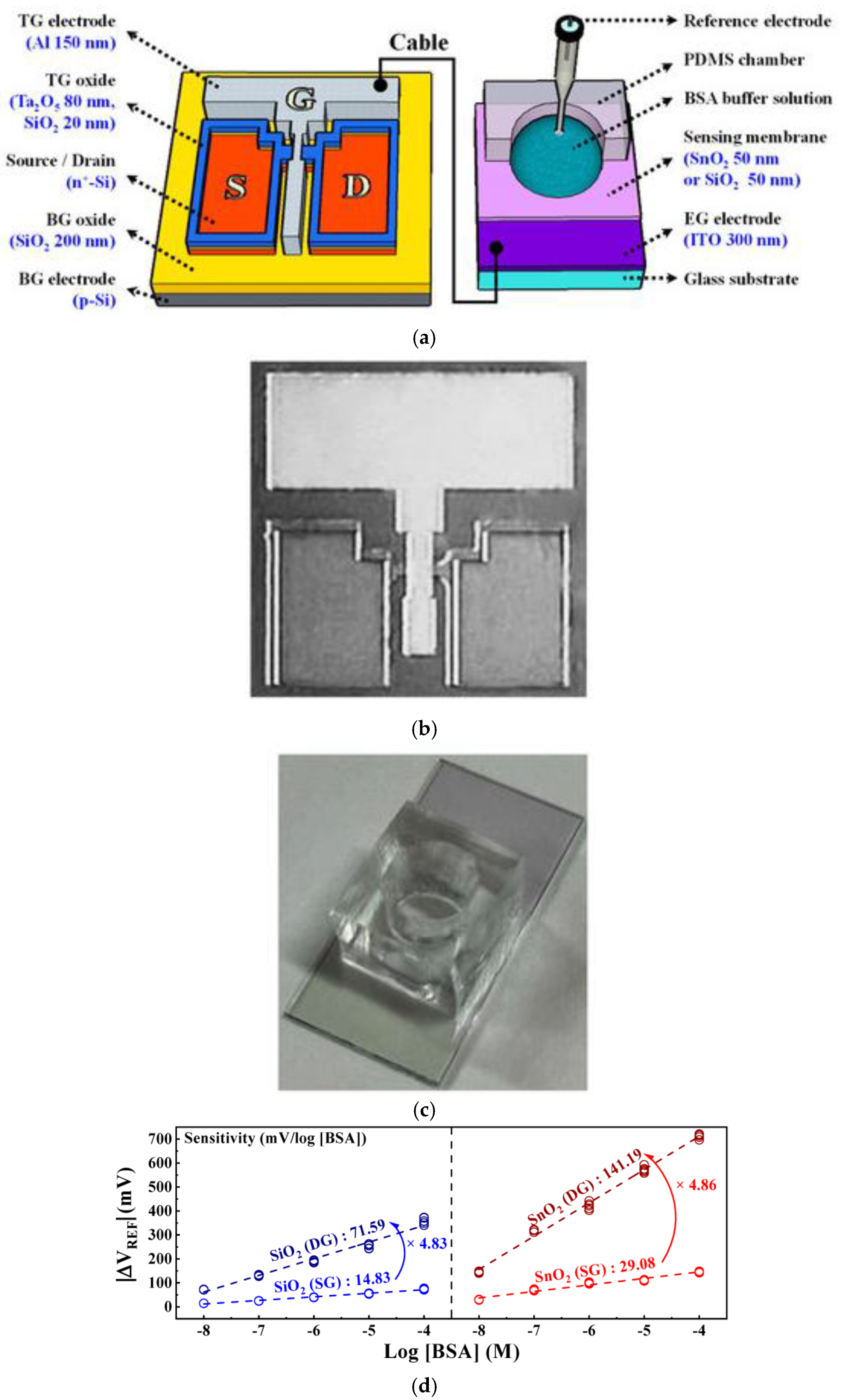
Recently, another oxide has been investigated to become a sensitive layer within an ISFET, namely tin oxide SnO2. However, the resulted ISFET device combined multiple oxides to decorate both top gate (TG) and bottom gate (BG) space [105]. A high-k dielectric material was selected in the TG space: SiO₂ 20 nm covered by Ta₂O₅ 80 nm, to improve the silicon/oxide interface, especially near the channel location. The SnO2 50 nm was used as sensitive insulator for an extended gate configuration. To achieve a 5:1 amplification ratio, the top oxides were engineered to possess an equivalent oxide thickness less than one-fifth that of the SiO₂ film from the bottom gate, Figure 18a.
The starting substrate for the sensitive part was a glass wafer covered by 300 nm indium tin oxide (ITO), then coated by 50 nm SnO2 by radio-frequency magnetron sputtering. Further functionalization added some OH groups on the surface, followed by APTES exposure, under the vapor-phase reaction method [106]. The final ISFET structure is presented in Figure 18b, and the BSA biosensor aided by ISFET with extended gate is shown in Figure 18c. When the ISFET transistor was operated without analyte, in the Single Gate (SG) configuration, it offered slightly better electrical device parameters than when it was Double Gate (DG) operated, giving just one example: SS|SG = 137 mV/dec < SS|DG = 213 mV/dec [105]. From the sensing point of view, the situation reversed for SnO2 based biosensor DG actioned. DG ISFET with sensitive SnO2 reached a maximum super-Nerstian sensitivity of 141.19 mV / decade of BSA concentration, versus the optimal SG variant that reached 29.08 mV / decade of BSA concentration, Figure 18d. However, Figure 18d also reveals inferior sensitivities for the DG ISFET with sensitive SiO2 reaching 71.59 mV/dec, while a minimum sub-Nernstian sensitivity of 14.83 mV /dec is offered by the biosensor with SiO2 layer acted by a single gate.
The 10 times sensitivity amplification, only in the presence of SnO2 layer, open new visions of biosensors without any additional external electronic circuits.
Another technological issue faced for the reliable realization of ISFETs is the occurrence of traps and defects at the semiconductor/oxide interfaces. These defects considerably reduce the current and the sensitivity of the sensor. Usually, thermal treatments up to 800 0C are applied for standard MOS transistors [52,107], but these methods are no longer compatible with the co-integration of sensitive materials, especially biomaterials. Recent state-of-the-art approaches employing UV radiation to remove oxide-trapped charges have yielded satisfactory results [108]. However, the time processing for a device-to-device calibration took 17 hours of UV radiation per ISFET transistor.
Nanostructured materials have also been cleverly integrated to achieve super Nernstian sensitivity by a label-free sensor, accompanied by double gate CMOS transistor. The sensor contained silicon nanowires arrays co-integrated on silicon on insulator (SOI) wafer, to detect the C-reactive protein (CRP). The sensor shows excellent stability (20pA/min) and an outstanding current sensitivity up to 1.2 nA/decade for CRP proteins, in the linear range of detection [109]. Silicon nano-wires based sensors were applied for the detection of other proteins, too, like troponin [110], deoxyri-bonucleic acid (DNA) [111], micro-RNA [112], viruses [113], and also it has been used for the CRP detection, but for poorer concentration range [114]. The linearity interval of detection was 60 ng/mL - 100 μg/mL, covering the whole concentration range of human CRP, from the clinical samples [109].
Another target for the near future is reaching a sub-pico-molar detection limit. Sensors based on silicon junctionless transistors in nanowire configuration were able to detect concentrations as low as 580 zM zeptomolar of the streptavidin protein, at a close level to a single molecule detection [115,116].
As a conclusion to this section, it can be said that the development of ISFET sensors in the future will necessarily be interdisciplinary, combining micro- and nano-electronics, ultimate scaled nano-transistors [117], nanomaterials, nanoporous or nano-structured structures with increasingly refined receptors.
6. Conclusions
The paper reviewed the evolution of chemosensors with ion-sensitive transistors, like ISFETs, which integrate a sensitive layer made by nanoporous, nanostructured or specific oxides, near the electronic device. One of the main technological goals was to highlight those methods capable of anchoring the nanoporous layer to the substrate, usually a Si-wafer. The general technique would consist of depositing metal layers with high adhesion to the substrate, by classical microelectronics methods, which have proven reliable over time: chemical vacuum deposition, lift-off, sputtering, laser deposition. The usual thicknesses of the deposited metal vary in the range of 4 nm - 90 nm. Then, the surface of the metal electrode is converted into nanoporous oxide, with deep anchors of nanotubes from the constituent material. For this purpose, an electrochemical cell is used, as inert as possible as the material of the cell, in which the surface of the metal that must become nanoporous plays the role of the working electrode. Using various electrochemical currents, various polarization voltages and a wide range of electrolytes, various porosities, various geometries, which have an exponentially multiplied surface and are sensitive to an analyte, were obtained. By combining material optimizations with the use of extremely small transistors, a quasi-uni-molecular detection limit can be achieved. The use of Si nanowire transistors has pushed this detection limit to the atto-molar (10-18 M) and even zepto-molar (10-21 M) range for streptavidin detection. On the other hand, the ISFETs actioned by two gates, which includes sensitive oxide of SnO2 too, offers a maximum super-Nernstian sensitivity of 141.19 mV/dec. This 10 times sensitivity amplification opens the further development of biosensors free of additional external electrical circuits, with huge advantage for the device price.
It seems that the only successful way to develop chemosensors transistor-based in the future can only come from the collaboration of nanotechnologies with the study of new materials, biochemistry, micro-nano-electronics and co-integration technologies.
Author Contributions
For this research article, the individual contributions of authors were: Conceptualization, Paper writing, supervision, project administration, funding and review synthesis by C. Ravariu. Author has read and agreed to the published version of the manuscript.
Funding
This work was funded from the project „National Platform for Semiconductor Technologies”, contract no. G 2024-85828/390008/27.11.2024, SMIS code 304244, co-funded by the European Regional Development Fund under the Program for Intelligent Growth, Digitization, and Financial Instruments.
Institutional Review Board Statement
“Not applicable.”
Informed Consent Statement
“Not applicable.”
Data Availability Statement
“Not applicable.”
Conflicts of Interest
The authors declare no conflict of interest. The funders had no role in the design of the study, in the writing of the manuscript, or in the publishing decision.
References
- Vyas, P.B.; Zhao, C.; Dag, S.; Pal, A.; Bazizi, E.M.; Ayyagari-Sangamalli, A. Next Generation Gate-all-around Device Design for Continued Scaling Beyond 2 nm Logic. International Conference on Simulation of Semiconductor Processes and Devices (SISPAD) Kobe, Japan 2023, 1, 57–60. [Google Scholar] [CrossRef]
- Refai-Ahmed, G.; Zhirnov, V.V.; Park, S.B.; Helmy, A.S.; Sammakia, B.; Ghose, K.; Ang, J.A.; Bonilla, G.; Mahdi, T.; Wieser, J.; Ramalingam, S. New Roadmap for Microelectronics: Charting the Semiconductor Industry’s Path Over the Next 5, 10, and 20 Years. 26th IEEE Electronics Packaging Technology Conference EPTC, Singapore, 2024, 1, 1260–1266. [Google Scholar] [CrossRef]
- Panahi, A.; Ghafar-Zadeh, E. Emerging Field-Effect Transistor Biosensors for Life Science Applications. Bioengineering 2023, 10, 793. [Google Scholar] [CrossRef] [PubMed]
- Ravariu, C. Current Status of Field-Effect Transistors for Biosensing Applications. Biosensors 2022, 12, 1081. [Google Scholar] [CrossRef] [PubMed]
- Rai, H.; Singh, K.R.B.; Natarajan, A.; Pandey, S.S. Advances in field effect transistor based electronic devices integrated with CMOS technology for biosensing. Talanta Open 2025, 11, 8, 100394. [Google Scholar] [CrossRef]
- Yang, J.; Yu, C. Fundamentals of chemical sensors and biosensors, Chapter 1, Editor(s): Jeong-Yeol Yoon, Chenxu Yu. Machine Learning and Artificial Intelligence in Chemical and Biological Sensing. Elsevier Science 2024, 1-21. pp. 1–21. [CrossRef]
- Musala, S.; Srinivasulu, A.; Appasani, B.; Ravariu, C. Low Power High Speed FINFET Based Differential Adder Circuits With Proposed Carry/Carrybar Structures. University Politehnica of Bucharest Scientific Bulletin Series C Electrical Engineering and Computer Science 2023, 85, 335–353. [Google Scholar]
- Ravariu, C.; Srinivasulu, A.; Mihaiescu, D.E.; Musala, S. Generalized Analytical Model for Enzymatic BioFET Transistors. Biosensors 2022, 7, 474–478. [Google Scholar] [CrossRef] [PubMed]
- Butt, M.A.; Piramidowicz, R. Integrated Photonic Sensors for the Detection of Toxic Gasses - A Review. Chemosensors 2024, 12, 143. [Google Scholar] [CrossRef]
- Lee, J.; Lu, A.; Li, W.; Yu, S. NeuroSim V1.4: Extending Technology Support for Digital Compute-in-Memory Toward 1nm Node. IEEE Transactions on Circuits and Systems I: Regular Papers 2024, 71, 1733–1744. [Google Scholar] [CrossRef]
- Boughedda, A.; Pancheri, L.; Parmesan, L.; Gasparini, L.; Quarta, G.; Perenzoni, D.; Perenzoni, M. The Modeling of a Single-Electron Bipolar Avalanche Transistor in 150 nm CMOS. Sensors 2025, 25, 3354. [Google Scholar] [CrossRef]
- Gubanova, O.; Poletaev, A.; Komarova, N.; Grudtsov, V.; Ryazantsev, D.; Shustinskiy, M.; Shibalov, M. A. Kuznetsov, A novel extended gate ISFET design for biosensing application compatible with standard CMOS. Materials Science in Semiconductor Processing 2024, 177, 108387. [Google Scholar] [CrossRef]
- Ravariu, C.; Mihaiescu, D.; Morosan, A.; Vasile, B.S.; Purcareanu, B. Sulpho-Salicylic Acid Grafted to Ferrite Nanoparticles for n-Type Organic Semiconductors. Nanomaterials 2020, 10, 1787. [Google Scholar] [CrossRef] [PubMed]
- Kamani, T. , Baz, A.; Patel, S.K., Design of an Efficient Surface Plasmon Resonance Biosensor for Label-Free Detection of Blood Components. Plasmonics 2025, 20, 3147–3160. [Google Scholar] [CrossRef]
- Olajiga, O.M.; Jameson, S.B.; Carter, B.H.; Wesson, D.M.; Mitzel, D.; Londono-Renteria, B. Artificial Feeding Systems for Vector-Borne Disease Studies. Biology 2024, 13, 188. [Google Scholar] [CrossRef] [PubMed]
- Eidi, A. Design and evaluation of an implantable MEMS based biosensor for blood analysis and real-time measurement. Microsystem Technology 2023, 29, 857–864. [Google Scholar] [CrossRef]
- Yáñez, C.; DeMas-Giménez, G.; Royo, S. Overview of Biofluids and Flow Sensing Techniques Applied in Clinical Practice. Sensors 2022, 22, 6836. [Google Scholar] [CrossRef] [PubMed]
- Pelenis, D.; Barauskas, D.; Dzikaras, M.; Viržonis, D. Four-Channel Ultrasonic Sensor for Bulk Liquid and Biochemical Surface Interrogation. Biosensors 2024, 14, 66. [Google Scholar] [CrossRef] [PubMed]
- Leau, S. A.; Diaconu, I.; Lete, C.; Matei, C.; Lupu, S. Electro analysis of serotonin at platinum nanoparticles modified electrode. University Politehnica of Bucharest Scientific Bulletin Series C Electrical Engineering and Computer Science 2024, 86, 1–14. [Google Scholar]
- Kamal Eddin, F.B.; Fen, Y.W. The Principle of Nanomaterials Based Surface Plasmon Resonance Biosensors and Its Potential for Dopamine Detection. Molecules 2020, 25, 2769. [Google Scholar] [CrossRef] [PubMed]
- Ravariu, C.; Popescu, A.; Podaru, C.; Manea, E.; Babarada, F. The Nanopous Al2O3 Material Used for the Enzyme Entrapping in a Glucose Biosensor. XII Mediterranean Conference on Medical and Biological Engineering and Computing MEDICON 2010, Chalkidiki, Greece, Springer Proceedings, vol. 29, pp. 459-462.
- Ryazantsev, D.; Shustinskiy, M.; Sheshil, A.; Titov, A.; Grudtsov, V.; Vechorko, V.; Kitiashvili, I.; Puchnin, K.; Kuznetsov, A.; Komarova, N. A Portable Readout System for Biomarker Detection with Aptamer-Modified CMOS ISFET Array. Sensors 2024, 24, 3008. [Google Scholar] [CrossRef] [PubMed]
- Ravariu, C.; Podaru, C.; Manea, E. Design and technological characterization aspects of a gluco-detector BioFET. 32nd IEEE International Semiconductor Conference, Sinaia, Romania 2009, 281-284. [CrossRef]
- Minamiki, T.; Sekine, T.; Aiko, M.; Su, S.; Minami, T. An organic FET with an aluminum oxide extended gate for pH sensing. Sensors and Materials 2019, 31, 99–106. [Google Scholar] [CrossRef]
- Pushparaj, K.; Di Zazzo, L.; Allegra, V.; Capuano, R.; Catini, A.; Magna, G.; Paolesse, R.; Di Natale, C. Detection of Ascorbic Acid in Tears with an Extended-Gate Field-Effect Transistor-Based Electronic Tongue Made of Electropolymerized Porphyrinoids on Laser-Induced Graphene Electrodes. Chemosensors 2025, 13, 108. [Google Scholar] [CrossRef]
- Abhinav, V.; Naik, T.R. Low-Cost, Point-of-Care Potassium Ion Sensing Electrode in EGFET Configuration for Ultra-High Sensitivity. IEEE Access 2024, 12, 121837–121845. [Google Scholar] [CrossRef]
- Barmpakos, D.; Apostolakis, A.; Jaber, F.; Aidinis, K.; Kaltsas, G. Recent Advances in Paper-Based Electronics: Emphasis on Field-Effect Transistors and Sensors. Biosensors 2025, 15, 324. [Google Scholar] [CrossRef] [PubMed]
- Hashim, S. B., Aqilah Azlan; Mahzan, N. H.; Zulkifli, Z.; Zulkefle, *!!! REPLACE !!!*; M.A., *!!! REPLACE !!!*; Herman, S.H. Understanding the Extended-gate FET pH Sensor Sensing Mechanism through Equivalent Circuit Simulation in LTSpice. IEEE International Conference on Automatic Control and Intelligent Systems (I2CACIS), Shah Alam, Malaysia. 2024; 373–378. [Google Scholar] [CrossRef]
- Pan, T.M.; Lin, L-A.; Ding, H-Y.; Her, J-L.; Pang, S-T. A simple and highly sensitive flexible sensor with extended-gate field-effect transistor for epinephrine detection utilizing InZnSnO sensing films. Talanta 2024, 275, 126178. [Google Scholar] [CrossRef] [PubMed]
- Zheng, A.L.T. , Teo, E.Y.L., Seenivasagam, S., Hung, Y.P., Boonyuen S., Chung E.L.T., Lease J., Andou Y. Nanostructures embedded on porous materials for the catalytic reduction of nitrophenols: a concise review. Journal of Porous Materials 2024, 31, 1557–1575. [Google Scholar] [CrossRef]
- Feng, S.; Luo, Q.; Song, X. An antibody nanopore-enabled microsensor for detection of osteoprotegerin. Japanese Journal of Applied Physics 2024, 63, 11, 117001. [Google Scholar] [CrossRef]
- McBride, S.A. , Temprano-Coleto F., Kaneelil P.R., Knopp R., Taylor A.J., Storey-Matsutani M.A., Wilson J.L., Saleh M.S., Konicek, A.R. Effect of capillary number and viscosity ratio on multiphase displacement in microscale pores. Phys. Rev. Fluids 2025, 10, 054201. [Google Scholar] [CrossRef]
- Lee, M.; Lee, M.; Kim, S.; Park, N. Stimuli-Responsive DNA Hydrogel Design Strategies for Biomedical Applications. Biosensors 2025, 15, 355. [Google Scholar] [CrossRef] [PubMed]
- Shahid, Z.; Veenuttranon, K.; Lu, X.; Chen, J. Recent Advances in the Fabrication and Application of Electrochemical Paper-Based Analytical Devices. Biosensors 2024, 14, 561. [Google Scholar] [CrossRef] [PubMed]
- Shahbaz, A., Hussain. Immobilized Enzymes-Based Biosensing Cues for Strengthening Biocatalysis and Biorecognition. Catal. Lett. 2022, 152, 2637–2649. [Google Scholar] [CrossRef]
- Ravariu, C.; Manea, E.; Parvulescu, C.; Babarada, F.; Popescu, A. Titanium dioxide nanotubes on silicon wafer designated for GOX enzymes immobilization. Digest Journal of Nanomaterials and Biostructures 2011, 6, 2, 703–707. [Google Scholar]
- Wang, B.; Zhang, J.; Dong, S. Silica sol–gel composite film as an encapsulation matrix for the construction of an amperometric tyrosinase-based biosensor. Biosensors and Bioelectronics 2000, 15, 7–8, 397. [Google Scholar] [CrossRef] [PubMed]
- Gupta, R.; Chaudhury, N.K. Entrapment of biomolecules in sol–gel matrix for applications in biosensors: Problems and future prospects. Biosensors and Bioelectronics 2007, 22, 11, 2387–2399. [Google Scholar] [CrossRef] [PubMed]
- Ravariu, C.; Parvulescu, C.C.; Manea, E.; Tucureanu, V. Optimized Technologies for Cointegration of MOS ransistor and Glucose Oxidase Enzyme on a Si-Wafer. Biosensors 2021, 11, 12, 497. [Google Scholar] [CrossRef] [PubMed]
- Roelofs, K.G.; Wang, J.; Sintim, H.O.; Leea, V.T. Differential radial capillary action of ligand assay for high-throughput detection of protein-metabolite interactions. Proceedings of the National Academy of Sciences 2011, 108, 37, 15528–15533. [Google Scholar] [CrossRef] [PubMed]
- Chen, S.-J.; Lu, S.-Y.; Tseng, C.-C.; Huang, K.-H.; Chen, T.-L.; Fu, L.-M. Rapid Microfluidic Immuno-Biosensor Detection System for the Point-of-Care Determination of High-Sensitivity Urinary C-Reactive Protein. Biosensors 2024, 14, 283. [Google Scholar] [CrossRef] [PubMed]
- Mah, D.-G.; Oh, S.-M.; Jung, J.; Cho, W.-J. Enhancement of Ion-Sensitive Field-Effect Transistors through Sol-Gel Processed Lead Zirconate Titanate Ferroelectric Film Integration and Coplanar Gate Sensing Paradigm. Chemosensors 2024, 12, 134. [Google Scholar] [CrossRef]
- Prall, K. Chapter: Mobile Ion Contamination. In book: CMOS Plasma and Process Damage. Springer Cham. [CrossRef]
- Yeh, J.-T.; Hsiao, C.-Y.; Lee, H.-W.; Kuo, C.-F. Comparison between Different Configurations of Reference Electrodes for an Extended-Gate Field-Effect Transistor pH Sensor. ACS Omega 2025, 10, 8433−8439. [Google Scholar] [CrossRef] [PubMed]
- Bharathi, G.; Hong, S. Gate Engineering in Two-Dimensional (2D) Channel FET Chemical Sensors: A Comprehensive Review of Architectures, Mechanisms and Materials. Chemosensors 2025, 13, 217. [Google Scholar] [CrossRef]
- Hu, W.-P.; Yang, Y.-Q.; Lee, C.-H.; Vu, C.-A.; Chen, W.-Y. Comparing solution-gate and bottom-gate nanowire field-effect transistors on pH sensing with different salt concentrations and surface modifications. Talanta 2024, 271, 125731. [Google Scholar] [CrossRef] [PubMed]
- Garika, V.; Babbar, S.; Samanta, S.; Harilal, S.; Lerner, A.E.; Rotfogel, Z.; Pikhay, E.; Shehter, I.; Elkayam, A.; Bashouti, M.Y.; Akabayov, B.; Ron, I.; Hazan, G.; Roizin, Y.; Shalev, G. Addressing the challenge of solution gating in biosensors based on field-effect transistors. Biosensors and Bioelectronics 2024, 265, 116689. [Google Scholar] [CrossRef] [PubMed]
- Bergveld, P. Development, operation and application of the ion sensitive field effect transistor as a tool for electrophysiology. IEEE Trans. Biomed. Eng. BME 1972, 19, 342–351. [Google Scholar] [CrossRef] [PubMed]
- Janićijević, Ž.; Baraban, L. Integration Strategies and Formats in Field-Effect Transistor Chemo- and Biosensors: A Critical Review. ACS Sensors 2025, 10, 4, 2431–2452. [Google Scholar] [CrossRef] [PubMed]
- Mansouri, S. , Alharbi, Y., Alqahtani, A. Nanomaterials Connected to Bioreceptors to Introduce Efficient Biosensing Strategy for Diagnosis of the TORCH Infections: A Critical Review. Critical Reviews in Analytical Chemistry 2024, 55, 4, 603–620. [Google Scholar] [CrossRef] [PubMed]
- Bergveld, P. Thirty years of ISFETOLOGY What happened in the past 30 years and what may happen in the next 30 years. Sensors and Actuators B 2003, 88, 1–20. [Google Scholar] [CrossRef]
- Ravariu, C. MOSFET with tips and tricks. e-Book Politehnica Press Publisher 2023, Bucharest, Romania, pp. 56-59.
- R.E.G. van Hal, J.C.T. Eijkel, P. Bergveld. A novel description of ISFET sensitivity with the buffer capacity and double layer capacitance as key parameters. Sensors and Actuators B 1995, 24/25, 201–205.
- M. Esashi, T. Matsuo. Integrated micro multi ion sensor using field effect of semiconductor. IEEE Trans. Biomed. Eng. BME 1978, 25, 184–192.
- Sakai, T. Ion sensitive FET with a silicon–insulator silicon structure. Proceedings of the Transducer-87.
- Hyun, T.-H.; Cho, W.-J. High-Performance FET-Based Dopamine-Sensitive Biosensor Platform Based on SOI Substrate. Biosensors 2023, 13, 516. [Google Scholar] [CrossRef] [PubMed]
- J.M. Chovelon, N. Jaffrezic-Renault, Y. Cros, J.J. Fombon, D. Pedone, Monitoring of ISFET encapsulation aging by impedance measurements. Sensors and Actuators B: Chemical 1991, 3, 43–50. [CrossRef]
- Nandanwar, S.; Lee, S.; Park, M.; Kim, H.J. Label-Free Extended Gate Field-Effect Transistor for Sensing Microcystin-LR in Freshwater Samples. Sensors 2025, 25, 1587. [Google Scholar] [CrossRef] [PubMed]
- Popescu, M.; Ravariu, C.; Hascsi, Z. First and Second Order Digital Circuits with Neuronal Models under Pulses Train Stimulus. Romanian Journal of Information Science and Technology ROMJIST 2025, 28, 223–232. [Google Scholar] [CrossRef]
- Hoover, T.M. Development of macroporous silicon for bio-chemical sensing applications. Journal of Microelectronic Engineering Conference 2005, 15, 78–86. [Google Scholar]
- Manea, E.; Podaru, C.; Popescu, A.; Budianu, E.; Purica, M.; Babarada, F.; Parvulescu, C. Nano-Porous Silicon for Sensors and Solar Cells. AIP Conf. Proceedings 2007, 899, 759. [Google Scholar] [CrossRef]
- Zavatski, S.; Popov, A.I.; Chemenev, A.; Dauletbekova, A.; Bandarenka, H. Wet Chemical Synthesis and Characterization of Au Coatings on Meso- and Macroporous Si for Molecular Analysis by SERS Spectroscopy. Crystals 2022, 12, 1656. [Google Scholar] [CrossRef]
- Ramírez-González, F.; García-Salgado, G.; Rosendo, E.; Díaz, T.; Nieto-Caballero, F.; Coyopol, A.; Romano, R.; Luna, A.; Monfil, K.; Gastellou, E. Porous Silicon Gas Sensors: The Role of the Layer Thickness and the Silicon Conductivity. Sensors 2020, 20, 4942. [Google Scholar] [CrossRef] [PubMed]
- Lu, H.; Jin, M.; Zhang, Z.; Wu, S.; Shui, L. Wafer-Scale Fabrication and Transfer of Porous Silicon Films as Flexible Nanomaterials for Sensing Application. Nanomaterials 2022, 12, 1191. [Google Scholar] [CrossRef] [PubMed]
- Gonzalez-Rodriguez, R.; Hathaway, E.; Coffer, J.L.; del Castillo, R.M.; Lin, Y.; Cui, J. Gold Nanoparticles in Porous Silicon Nanotubes for Glucose Detection. Chemosensors 2024, 12, 63. [Google Scholar] [CrossRef]
- Jin, B.; Liao, L.; Shen, X.; Mei, Z.; Du, Q.; Liang, L.; Lei, B.; Du, J. Advancement in Research on Silicon/Carbon Composite Anode Materials for Lithium-Ion Batteries. Metals 2025, 15, 386. [Google Scholar] [CrossRef]
- Awawdeh, K.; Buttkewitz, M.A.; Bahnemann, J.; Segal, E. Enhancing the performance of porous silicon biosensors: the interplay of nanostructure design and microfluidic integration. Microsystems & Nanoengineering 2024, 10, 100. [Google Scholar] [CrossRef] [PubMed]
- Kaczmarek, K.A.; Kosewski, G.; Dobrzyńska, M.; Drzymała-Czyż, S. Lactoferrin Production: A Systematic Review of the Latest Analytical Methods. Appl. Sci. 2025, 15, 4540. [Google Scholar] [CrossRef]
- Babarada, F.; Ravariu, C.; Bajenaru, A.; Manea, E. From simulations to masks for a BioFET design. IEEE, 2010. [Google Scholar] [CrossRef]
- Sen, A.; Shim, J.; Bala, A.; Park, H.; Kim, S. Boosting Sensitivity and Reliability in Field-Effect Transistor-Based Biosensors with Nanoporous MoS2 Encapsulated by Non-Planar Al2O3. Advanced Functional Materials 2023, 33, 42, 2301919:1–10. [Google Scholar] [CrossRef]
- Khanna, V.K. A plausible ISFET drift-like aging mechanism for Al2O3 humidity sensor. Sensors and Actuators B: Chemical 2015, 213, 351–359. [Google Scholar] [CrossRef]
- Hassan, E.A.; Abdolkader, T.M. A review of ion-sensitive field effect transistor (ISFET) based biosensors. International Journal of Materials Technology and Innovation 2023, 3, 3, 69–84. [Google Scholar] [CrossRef]
- Prem, A.R.; Elshafie, H.; Changalasetty, S.B.; Mubarakali, A. Optimizing Thermal Characteristics and Mobility in Sub-10 nm β-(AlxGa1−x)2O3/Ga2O3 Tri-Metal MODFETs for Advanced Biosensing Applications. ECS Journal of Solid State Science and Technology 2025, 14, 017005. [Google Scholar] [CrossRef]
- Deeban, Y. Effectiveness of CAD-CAM Milled Versus DMLS Titanium Frameworks for Hybrid Denture Prosthesis: A Narrative Review. J. Funct. Biomater 2024, 15, 376. [Google Scholar] [CrossRef] [PubMed]
- Marin, E.; Lanzutti, A. Biomedical Applications of Titanium Alloys: A Comprehensive Review. Materials 2024, 17, 114. [Google Scholar] [CrossRef] [PubMed]
- Ravariu, C.; Manea, E.; Babarada, F. Masks and metallic electrodes compounds for silicon biosensor integration. Journal of Alloys and Compounds 2017, 697, 72–79. [Google Scholar] [CrossRef]
- Yang, D-J; Kim, H-G.; Cho, S-J.; Choi, W-I. Thickness-conversion ratio from titanium to TiO2 nanotube fabricated by anodization method. Materials Letters 2008, 62, 775. [CrossRef]
- Yang, C.-C.; Chen, K.-Y.; Su, Y.-K. TiO2 Nano Flowers Based EGFET Sensor for pH Sensing. Coatings 2019, 9, 251. [Google Scholar] [CrossRef]
- Zulkefle, M.A.; Rahman, R.A.; Rusop, M.; Abdullah, W.F.H.; Herman, S.H. Porous TiO2 thin film for EGFET pHsensing application. Int. J. Eng. Technol. 2018, 7, 112–114. [Google Scholar] [CrossRef]
- Ravariu, C.; Manea, E.; Pârvulescu, C.; Țucureanu, V.; Appasani, B.; Srinivasulu, A. Preliminary simulations and experiments of enzymatic MOS biosensors. Proc. of IEEE Annual Conference of Semiconductors CAS, 2024; 301–304. [Google Scholar] [CrossRef]
- Ali, G.M. Interdigitated extended gate field effect transistor without reference electrode. Journal of Electronic Materials 2017, 46, 713–717. [Google Scholar] [CrossRef]
- Qi, J.; Zhang, H.; Ji, Z.; Xu, M.; Zhang, Y. ZnO nano-array-based EGFET biosensor for glucose detection. Appl. Phys. A 2015, 119, 807–811. [Google Scholar] [CrossRef]
- Guerra, E.M.; Mulato, M. Synthesis and characterization of vanadium oxide/hexadecylamine membrane and its application as pH-EGFET sensor. J. Sol-Gel Sci. Technol. 2009, 52, 315–320. [Google Scholar] [CrossRef]
- Jrar, J.A.; Bilal, M.; Butt, F.K.; Zhang, Z.; Din, A.U.; Hou, J. A novel 2D graphene oxide/manganese vanadium oxide nanocomposite-based PEC biosensor for selective detection of glucose. Journal of Alloys and Compounds 2025, 1021, 179595. [Google Scholar] [CrossRef]
- Yang, C.M. Yang, C.M.; Wei, C-H; Ughi, F.; Chang, J-Y.; Pijanowska, D.G.; Lai, C-S. High pH stability and detection of α-synuclein using an EGFET biosensor with an HfO2 gate deposited by high-power pulsed magnetron sputtering. Sensors and Actuators B: Chemical 2024, 416, 136006. [Google Scholar] [CrossRef]
- Kim, J.; Seung Rim, Y.; Chen, H.; Cao, H.H.; Nakatsuka, N.; Hinton, H.L.; Zhao, C.; Andrews, A.M.; Yang, Y.; Weiss, P.S. Fabrication of High-Performance Ultrathin In2O3 Film Field-Effect Transistors and Biosensors Using Chemical Lift-Off Lithography. ACS Nano 2015, 9, 4, 4572–4582. [Google Scholar] [CrossRef] [PubMed]
- Tang, T.; Liu, X.; Li, C.; Lei, B.; Zhang, D.; Rouhanizadeh, M.; Hsiai, T.; Zhou, C. Complementary Response of In2O3 Nanowires and Carbon Nanotubes to Low-Density Lipoprotein Chemical Gating. Appl. Phys. Lett. 2005, 86, 103903. [Google Scholar] [CrossRef]
- Curreli, M.; Li, C.; Sun, Y.; Lei, B.; Gundersen, M. A.; Thompson, M. E.; Zhou, C. Selective Functionalization of In2O3 Nanowire Material Devices for Biosensing Applications. J. Am. Chem. Soc. 2005, 127, 6922–6923. [Google Scholar] [CrossRef] [PubMed]
- Elkington, D.; Cooling, N.; Belcher, W.; Dastoor, P.C.; Zhou, X. Organic Thin-Film Transistor (OTFT)-Based Sensors. Electronics 2014, 3, 234–254. [Google Scholar] [CrossRef]
- Ravariu, C.; Istrati, D.; Mihaiescu, D.; Morosan, A.; Purcareanu, B.; Cristescu, R.; Trusca, R.; Vasile, B. Solution for green organic thin film transistors: Fe3O4 nano-core with PABA external shell as p-type film. Journal of Materials Science - Materials in Electronics 2020, 31, 4, 3063–3073. [Google Scholar] [CrossRef]
- Xiang, Z.; Wang, K.; Lu, J.; Wang, Z.; Jin, H.; Li, R.; Shi, M.; Wu, L.; Yan, F.; Jiang, R. Uniform Oxide Layer Integration in Amorphous IGZO Thin Film Transistors for Enhanced Multilevel-Cell NAND Memory Performance. Appl. Sci. 2024, 14, 2588. [Google Scholar] [CrossRef]
- Liu, J.; Xiong, X.; Li, H.; Huang, X.; Wang, Y.; Sheng, Y.; Liang, Z.; Yao, R.; Ning, H.; Wei, X. Application of Solution-Processed High-Entropy Metal Oxide Dielectric Layers with High Dielectric Constant and Wide Bandgap in Thin-Film Transistors. Micromachines 2024, 15, 1465. [Google Scholar] [CrossRef] [PubMed]
- Alam, F.; Ashfaq Ahmed, M.; Jalal, A.H.; Siddiquee, I.; Adury, R.Z.; Hossain, G.M.M.; Pala, N. Recent Progress and Challenges of Implantable Biodegradable Biosensors. Micromachines 2024, 15, 475. [Google Scholar] [CrossRef] [PubMed]
- Kosri, E.; Ibrahim, F.; Thiha, A.; Madou, M. Micro and Nano Interdigitated Electrode Array (IDEA)-Based MEMS/NEMS as Electrochemical Transducers: A Review. Nanomaterials 2022, 12, 4171. [Google Scholar] [CrossRef] [PubMed]
- Kuanaeva, R.M.; Vaneev, A.N.; Gorelkin, P.V.; Erofeev, A.S. Nanopipettes as a Potential Diagnostic Tool for Selective Nanopore Detection of Biomolecules. Biosensors 2024, 14, 627. [Google Scholar] [CrossRef] [PubMed]
- Qian, J.; Tan, R.; Feng, M.; Shen, W.; Lv, D.; Song, W. Humidity Sensing Using Polymers: A Critical Review of Current Technologies and Emerging Trends. Chemosensors 2024, 12, 230. [Google Scholar] [CrossRef]
- Lee, M.; Kim, S.H.; Kim, D.; Kim, H.J. Rapid and Easy Detection of Microcystin-LR Using a Bioactivated Multi-Walled Carbon Nanotube-Based Field-Effect Transistor Sensor. Biosensors 2024, 14, 37. [Google Scholar] [CrossRef] [PubMed]
- Riedel, V.; Hinck, S.; Peiter, E.; Ruckelshausen, A. Concept and Realisation of ISFET-Based Measurement Modules for Infield Soil Nutrient Analysis and Hydroponic Systems. Electronics 2024, 13, 2449. [Google Scholar] [CrossRef]
- Guo, W.; Xia, B.; Peng, J. Multiscale Dynamic Diffusion Model for Ions in Micro- and Nano-Porous Structures of Fly Ash: Mineralization Experimental Research. Appl. Sci. 2024, 14, 5414. [Google Scholar] [CrossRef]
- Bellando, F.; Mele, L.J.; Palestri, P.; Zhang, J.; Ionescu, A.M.; Selmi, L. Sensitivity, Noise and Resolution in a BEOL-Modified Foundry-Made ISFET with Miniaturized Reference Electrode for Wearable Point-of-Care Applications. Sensors 2021, 21, 1779. [Google Scholar] [CrossRef] [PubMed]
- Zhang, J.; Rupakula, M.; Bellando, F.; Garcia, E.; Longo, J.; Wildhaber, F.; Herment, G.; Guérin, H.; Ionescu, A.M. Sweat Biomarker Sensor Incorporating Picowatt Three-Dimensional Extended Metal Gate Ion Sensitive FET Transistors. ACS Sens. 2019, 4, 2039–2047. [Google Scholar] [CrossRef] [PubMed]
- Totorica, N.; Hu, W.; Li, F. Simulation of different structured gate-all-around FETs for 2 nm node. IOP Engineering Research Express 2024, 6, 035326. [Google Scholar] [CrossRef]
- Wu, T.; Alharbi, A.; You, K. D.; Kisslinger, K.; Stach, E. A.; Shahrjerdi, D. Experimental Study of the Detection Limit in Dual Gate Biosensors Using Ultrathin Silicon Transistors. ACS Nano 2017, 11, 7142−7147. [Google Scholar] [CrossRef] [PubMed]
- Srivastava, A.; Mahanty, B.; Mohapatra, P.K.; Sen, D.; Ghosh, S.K.; Sengupta, A.; Verboom, W. Development of a dual sensitive N,N,N’,N’,N”,N”-hexa-n-octylnitrilotriacetamide (HONTA) based potentiometric sensor for direct thorium(IV) estimation. Sensors and Actuators B: Chemical 2024, 410, 135660. [Google Scholar] [CrossRef]
- Kim, Y.-U.; Cho, W.-J. Enhanced BSA Detection Precision: Leveraging High-Performance Dual-Gate Ion-Sensitive Field-Effect-Transistor Scheme and Surface-Treated Sensing Membranes. Biosensors 2024, 14, 141. [Google Scholar] [CrossRef] [PubMed]
- Firek, P.; Cichomski, M.; Waskiewicz, M.; Piwonski, I.; Kisielewska, A. ISFET Structures with Chemically Modified Membrane for Bovine Serum Albumin Detection. Circuit World 2018, 44, 45–50. [Google Scholar] [CrossRef]
- Go, J.; Nair, P. R.; Alam, M. A. Theory of Signal and Noise in Double-Gated Nanoscale Electronic pH Sensors. J. Appl. Phys. 2012, 112, 034516. [Google Scholar] [CrossRef] [PubMed]
- Hammond, P. A.; Cumming, D. R. S. Performance and system on-chip integration of an unmodified CMOS ISFET. Sens. Actuators, B 2005, 111, 254−258. [Google Scholar] [CrossRef]
- Capua, L.; Sprunger; Y; Elettro, H.; Risch, F.; Grammoustianou, A.; Midahuen, R.; Ernst, T.; Barraud, S.; Gill, R.; Ionescu, A.M. Label-Free C-Reactive Protein Si Nanowire FET Sensor Arrays With Super-Nernstian Back-Gate Operation. IEEE Transactions on Electron Devices 2022, 69, 4, 2159–2165. [CrossRef]
- Lee, I.; Luo, X.; Huang, J.; Cui, X.T.; Yun, M. Detection of cardiac biomarkers using single polyaniline nanowire-based conductometric biosensors. Biosensors 2012, 2, 205–220. [Google Scholar] [CrossRef] [PubMed]
- Zhang, G.-J.; Luo, Z. H. H.; Huang, M. J.; Tay, G. K. I.; Lim, E.-J.-A. Morpholino-functionalized silicon nanowire biosensor for sequence-specific label-free detection of DNA. Biosensors Bioelectronics 2010, 25, 11, 2447–2453. [Google Scholar] [CrossRef] [PubMed]
- Zhang, G.-J.; Chua, J. H.; Chee, R.-E.; Agarwal, A.; and Wong, S.M. Label-free direct detection of MiRNAs with silicon nanowire biosensors. Biosensors Bioelectronics 2009, 24, 8, 2504–2508. [Google Scholar] [CrossRef] [PubMed]
- Zhang, G.-J. Silicon nanowire biosensor for highly sensitive and rapid detection of Dengue virus. Sens. Actuators B, Chem. 2010, 146, 138–144. [Google Scholar] [CrossRef]
- Vitusevich, S. Characteristic frequencies and times, signal-to-noise ratio and light illumination studies in nanowire FET biosensors. Proc. IEEE Ukrainian Microw. Week UkrMW. [CrossRef]
- Georgiev, Y. M.; Petkov, N.; Yu, R.; Nightingale, A.M.; Buitrago, E.; Lotty, O.; deMello, J.C.; Ionescu, A.M.; Holmes, J.D. Detection of ultra-low protein concentrations with the simplest possible field effect transistor. Nanotechnology 2019, 30, 324001. [Google Scholar] [CrossRef] [PubMed]
- Mattioli, I.A.; Hassan, A.; Sanches, N.M.; Vieira, N.C.S.; Crespilho, F.N. Highly sensitive interfaces of graphene electrical-electrochemical vertical devices for on drop atto-molar DNA detection. Biosensors and Bioelectronics 2021, 175, 112851. [Google Scholar] [CrossRef] [PubMed]
- Alabdullah, M. G. K.; Elmessary, M. A.; Nagy, D.; Seoane, N. ; García-Loureiro, A-J.; Kalna, K. Scaling Challenges of Nanosheet Field-Effect Transistors Into Sub-2 nm Nodes. 2024; 12, 479–485. [Google Scholar] [CrossRef]
Figure 1.
The ISFET cross-section.
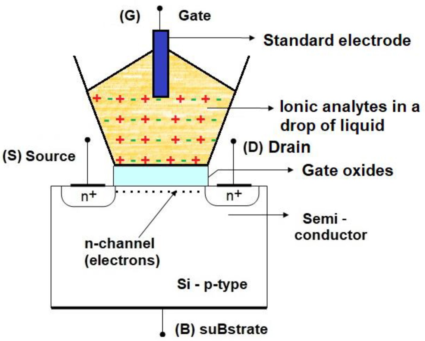
Figure 2.
The ΔV voltage deviation versus the NaCl concentration c: computed for HfO2, in comparison with experimental ΔV for different insulators - SiO2, Si3N4, Al2O3, Ta2O5, mentioned in literature [51]. .
Figure 2.
The ΔV voltage deviation versus the NaCl concentration c: computed for HfO2, in comparison with experimental ΔV for different insulators - SiO2, Si3N4, Al2O3, Ta2O5, mentioned in literature [51]. .
Figure 3.
(a) ISFET variant with the Source / Drain metal laterally spaced by a long diffusion from the gate electrode; (b) SOI ISFET variant with top contacts for Source and Drain and Back Gate, besides to the current vectors in normal conditions work.
Figure 3.
(a) ISFET variant with the Source / Drain metal laterally spaced by a long diffusion from the gate electrode; (b) SOI ISFET variant with top contacts for Source and Drain and Back Gate, besides to the current vectors in normal conditions work.
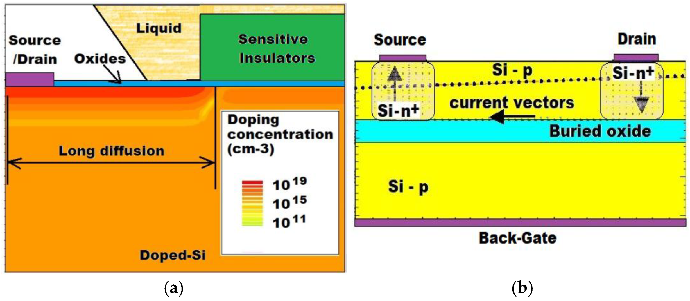
Figure 4.
SEM images for porous Si, different pores width, after anodization at a current density of (a) 30 mA/cm2; (b) 60 mA/cm2; (c) 100 mA/cm2. The main images presents the top views, while insets indicate the cross sections for each structure. (redrawn with MDPI permission from [62]).
Figure 4.
SEM images for porous Si, different pores width, after anodization at a current density of (a) 30 mA/cm2; (b) 60 mA/cm2; (c) 100 mA/cm2. The main images presents the top views, while insets indicate the cross sections for each structure. (redrawn with MDPI permission from [62]).
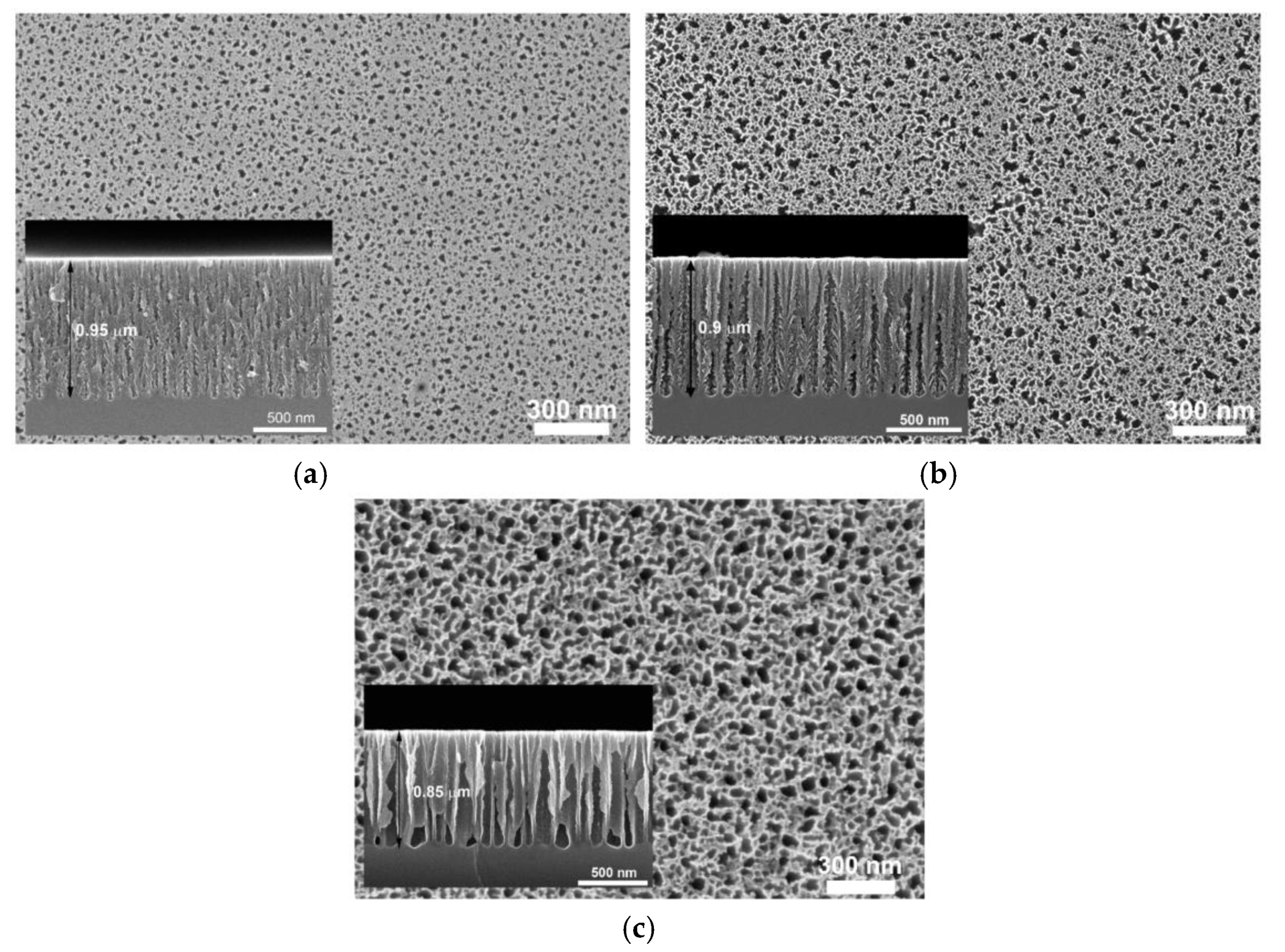
Figure 5.
(a) The designed geometric pattern; (b) the image of the final sensor with Al electrodes on PS. (redrawn with MDPI permission from [63]).
Figure 5.
(a) The designed geometric pattern; (b) the image of the final sensor with Al electrodes on PS. (redrawn with MDPI permission from [63]).
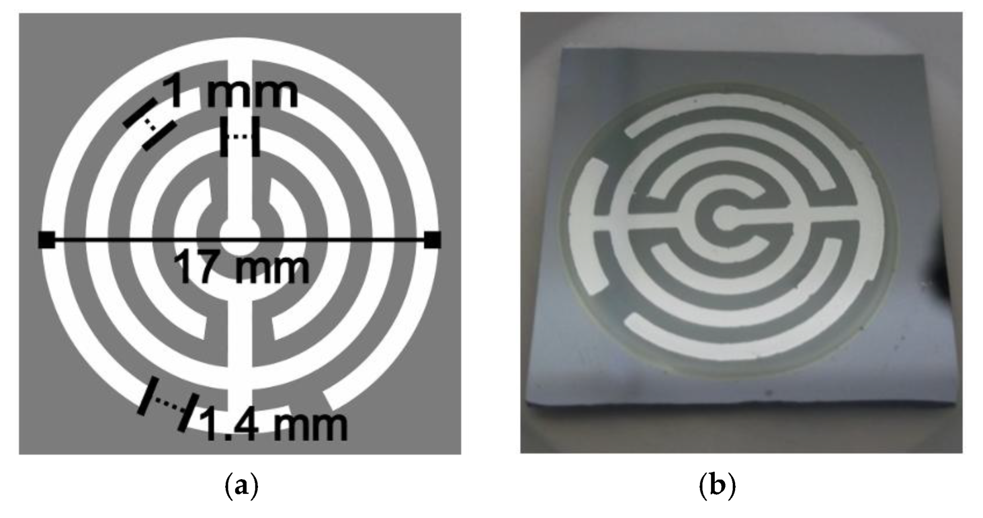
Figure 6.
SEM images of a patterned Si geometry for the following etchants ratio R: (a) 5:5, (b) 6:4, (c) 7:3, (d) 8:2, (e) 9:1 respectively (first line presents cross-sectional view, middle: high resolution of top view, bottom: top view); (f) PS thickness as a function of R. (redrawn with MDPI permission from [64]).
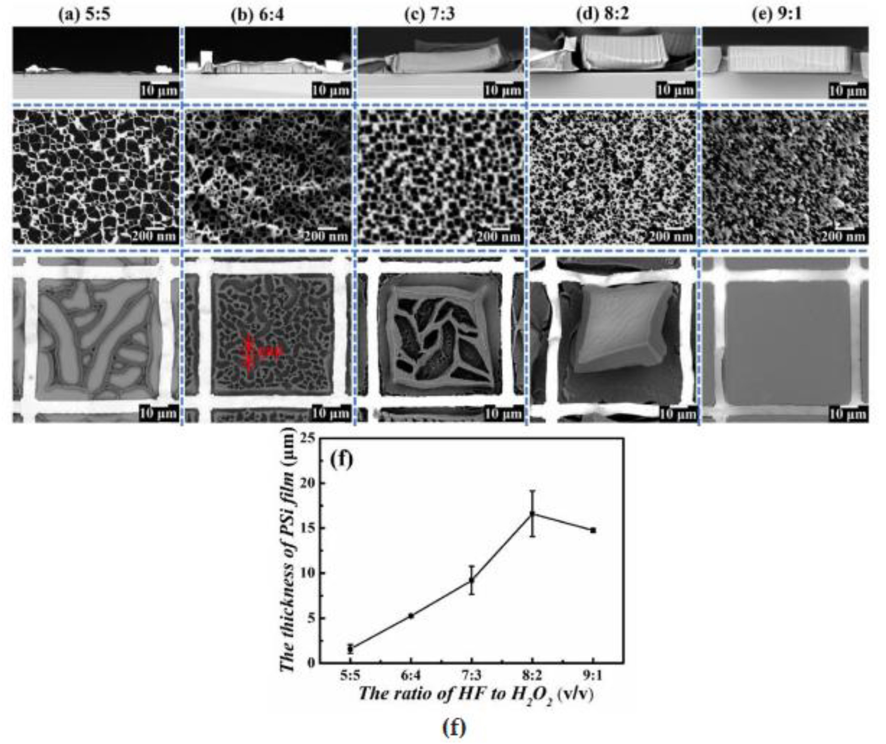
Figure 7.
(a) SEM image of the fabricated PSi-NTs; (b–d) Different images of PSi-NTs fabricated with uniform distributed gold nanoparticles, (e) HRTEM of PSi-NTs Au-NPs, containing Fast Fourier Transform (FFT) in inset; (f) the size distribution of the Au-NPs. (redrawn with MDPI permission from [65]). .
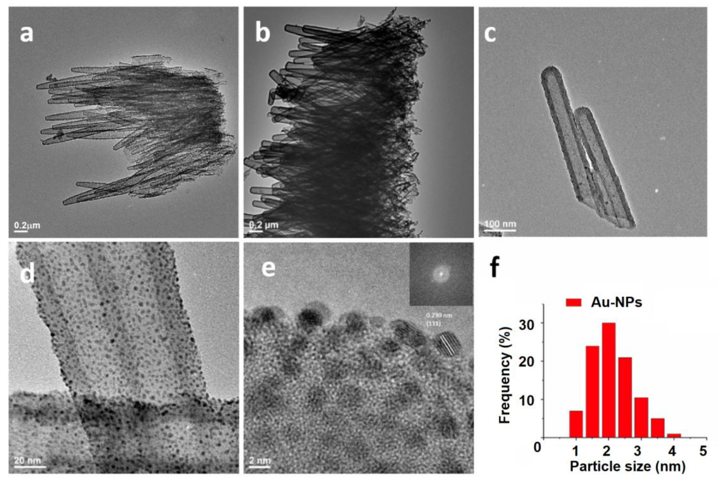
Figure 9.
(a) SEM image of the porous Al2O3 film, top view, (redrawn with Springer permission from [21]); (b) the experimental current-time dependence during the aluminium film anodization, (redrawn with IEEE permission from [69]).
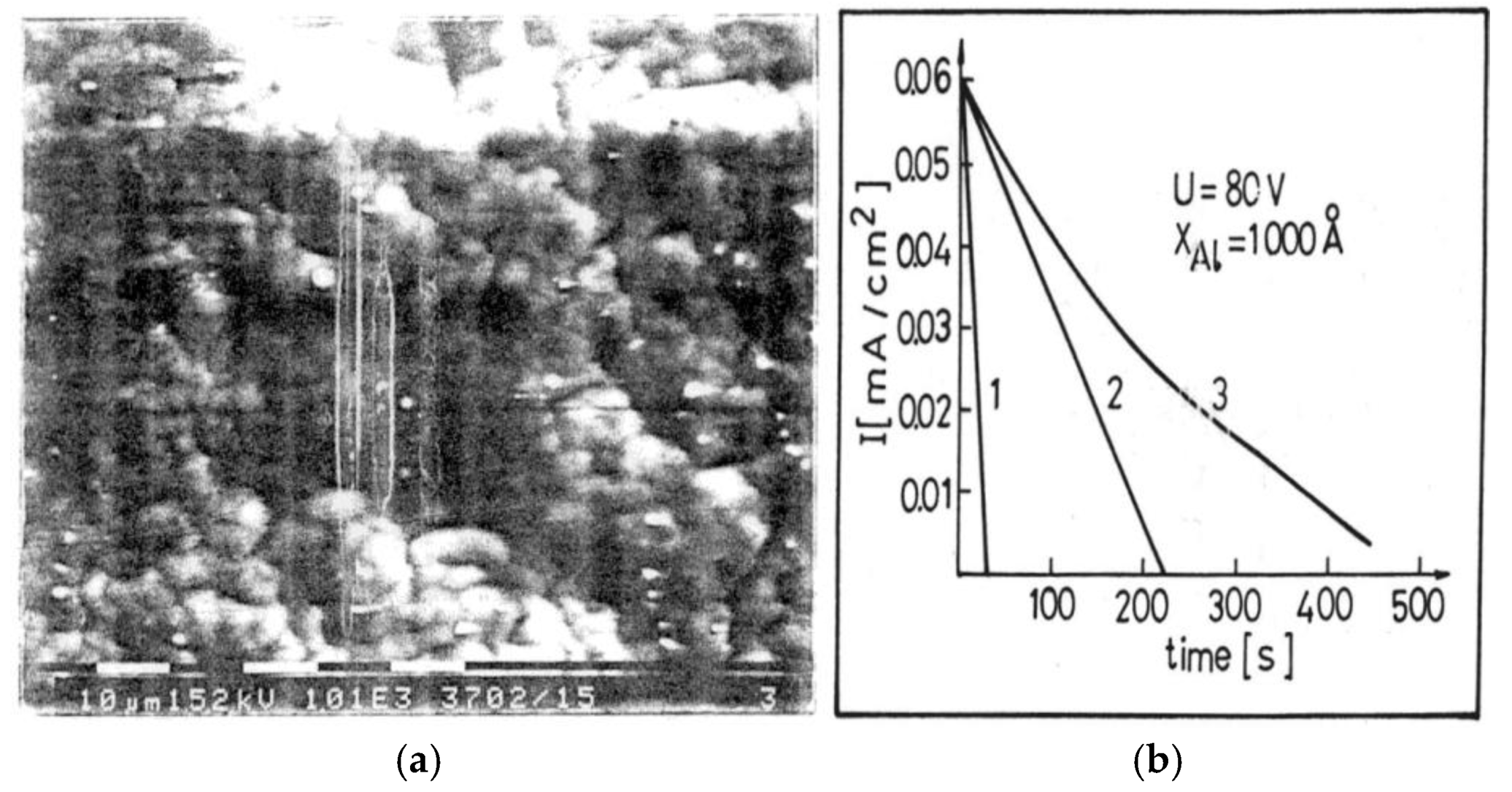
Figure 10.
SEM image of the Si/SiO2/ TiO2 /nafion/GOX sample: (a) top view at 1000 μm scale; (b) detail at 100 μm scale, (redrawn with Elsevier permission from [76]).
Figure 10.
SEM image of the Si/SiO2/ TiO2 /nafion/GOX sample: (a) top view at 1000 μm scale; (b) detail at 100 μm scale, (redrawn with Elsevier permission from [76]).
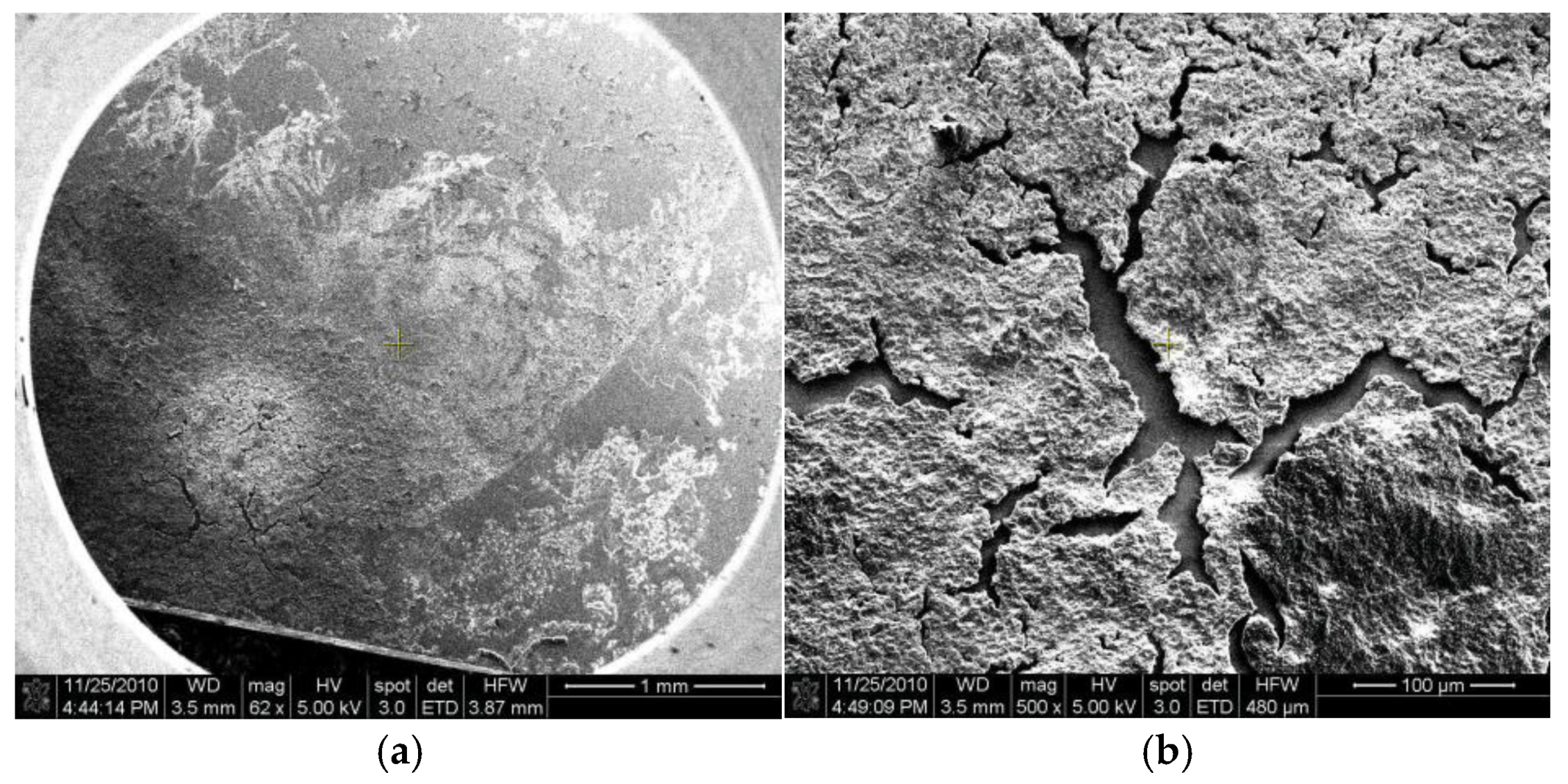
Figure 11.
(a) The TiO2 anatase phase achieved on Si-wafer, in a SEM top view image; (b) ATR-FTIR spectroscopy for the nano-structured TiO2 after anodization. (adapted and redrawn with permission from [76]).
Figure 11.
(a) The TiO2 anatase phase achieved on Si-wafer, in a SEM top view image; (b) ATR-FTIR spectroscopy for the nano-structured TiO2 after anodization. (adapted and redrawn with permission from [76]).
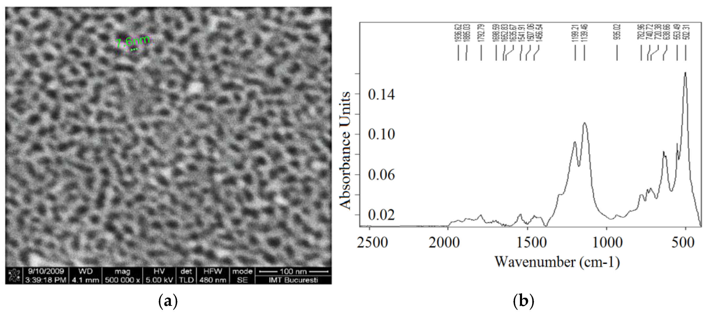
Figure 12.
(a) FTIR spectrum of the sample with glutaraldehyde on Si/SiO2/TiO2 structure; (b) SEM image of the enzyme membrane immobilized above. (adapted and redrawn after [76] with permission).
Figure 12.
(a) FTIR spectrum of the sample with glutaraldehyde on Si/SiO2/TiO2 structure; (b) SEM image of the enzyme membrane immobilized above. (adapted and redrawn after [76] with permission).
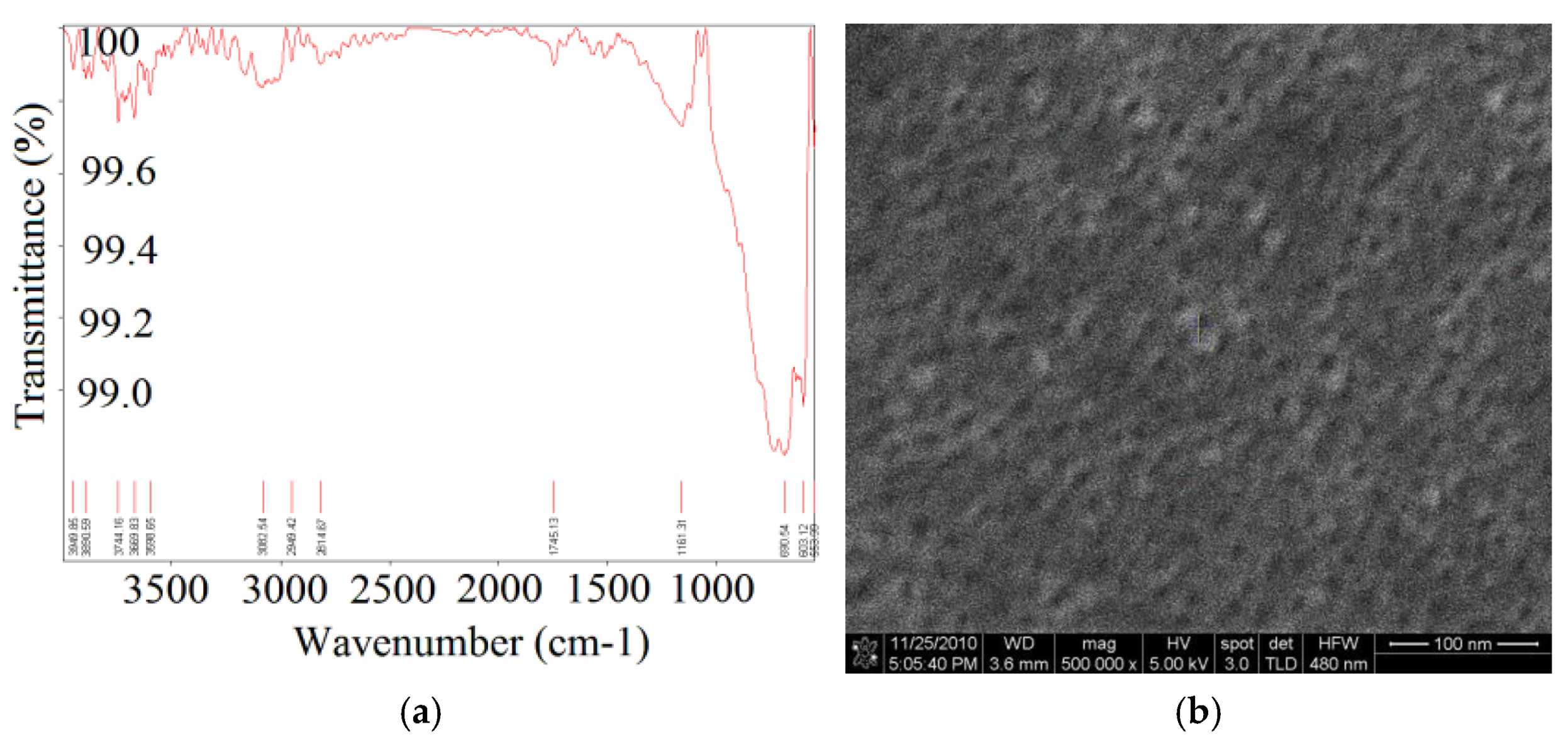
Figure 13.
(a) SEM image of the nano-structured- TiO2 film at an edge of a Si wafer, when the work electrode was biased between 2 - 25V; (redrawn after [76] with permission); (b) Our SEM images of the synthesized TiO2 film by anodization, after annealing at 800 °C in N2 atmosphere.
Figure 13.
(a) SEM image of the nano-structured- TiO2 film at an edge of a Si wafer, when the work electrode was biased between 2 - 25V; (redrawn after [76] with permission); (b) Our SEM images of the synthesized TiO2 film by anodization, after annealing at 800 °C in N2 atmosphere.
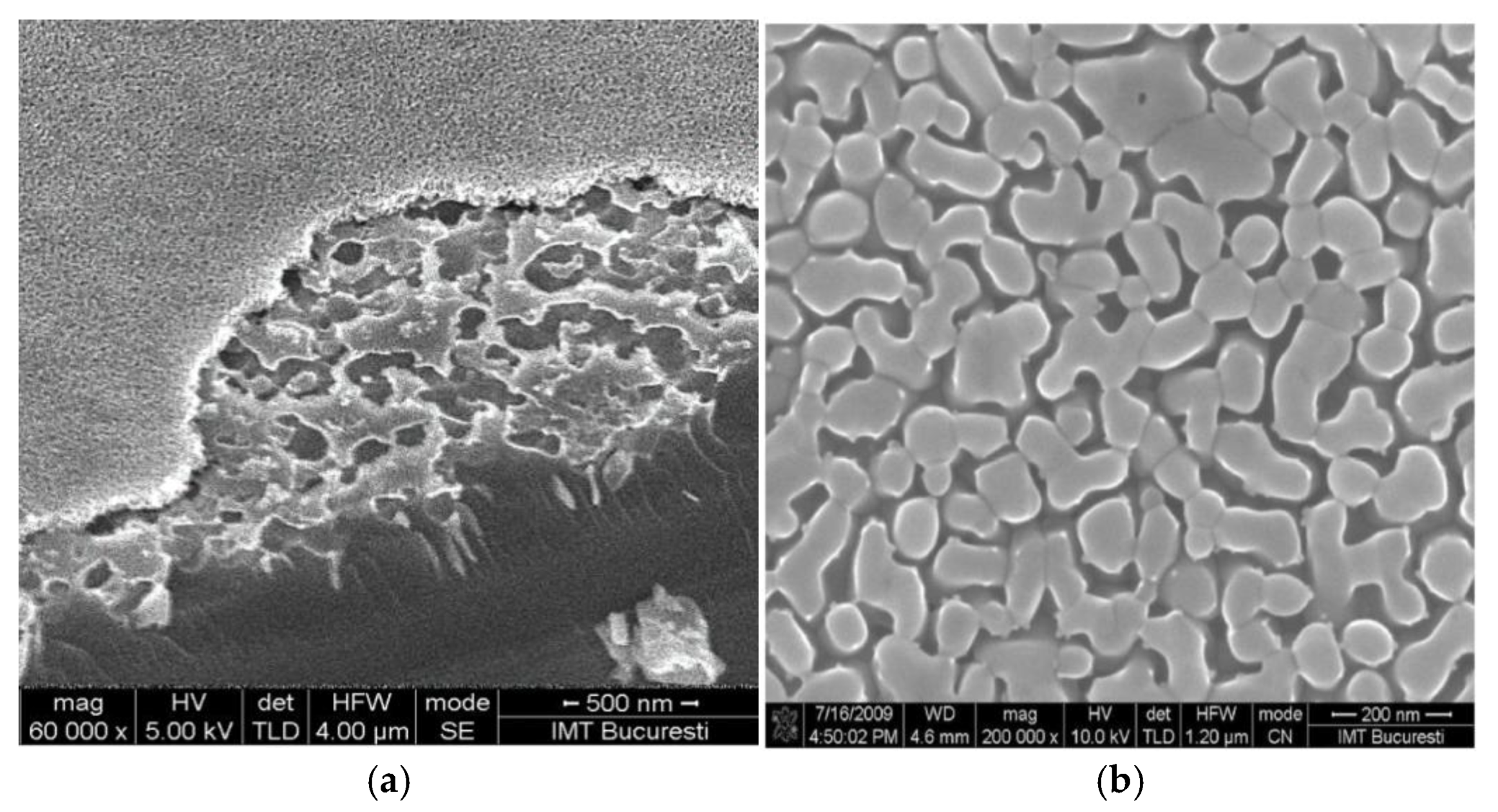
Figure 14.
FESEM images of titanium oxide nanotubes in a cross-section view, for different applied voltages of anodizing in an electrolyte aqueous solution: (A) 10 V, (B) 15 V, (C) 20 V, (D) 30 V, and in glycerol as electrolyte: (E) 5 V, (F) 10 V, (G) 15 V, (H) 20 V. (redrawn after [77] with permission).
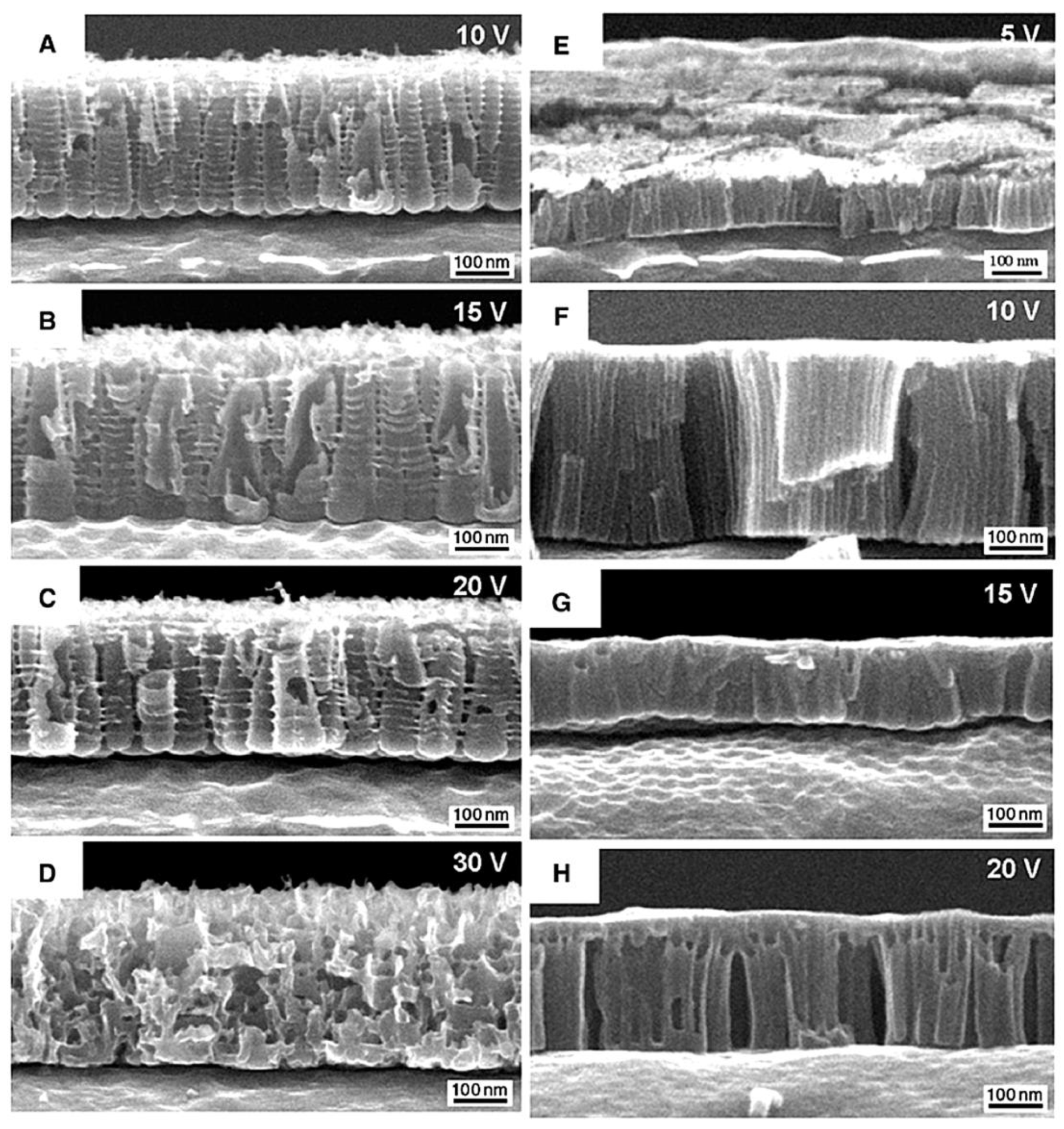
Figure 15.
(a) HR-SEM image, top view of the fabricated TiO2 nano-flowers, which show the randomly oriented flower-like nanostructures. (b) The high-magnified HR-SEM image. (redrawn after [78] with MDPI permission).
Figure 15.
(a) HR-SEM image, top view of the fabricated TiO2 nano-flowers, which show the randomly oriented flower-like nanostructures. (b) The high-magnified HR-SEM image. (redrawn after [78] with MDPI permission).
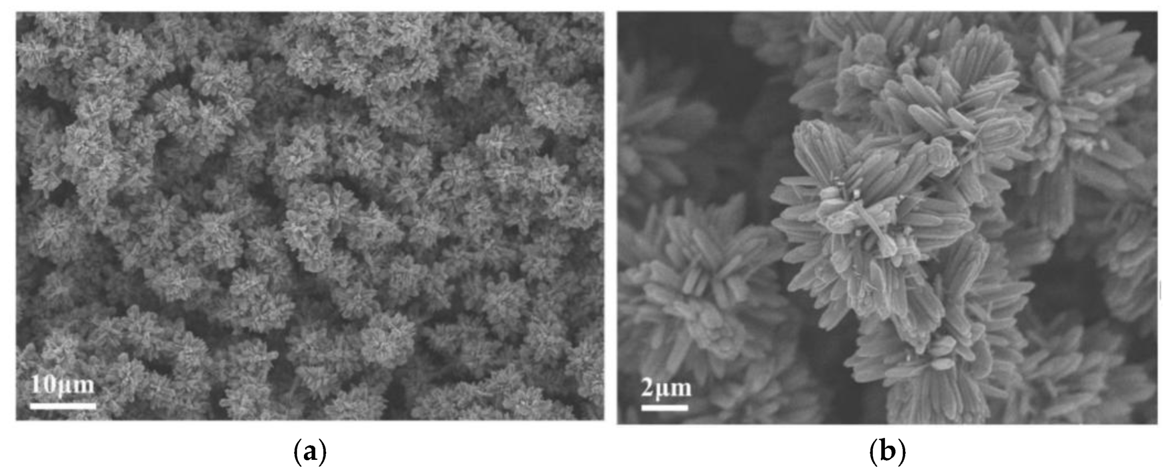
Figure 16.
Our SEM image of TiO2 nano-tubes grown from thick layers: (a) top view; (b) lateral view.
Figure 16.
Our SEM image of TiO2 nano-tubes grown from thick layers: (a) top view; (b) lateral view.
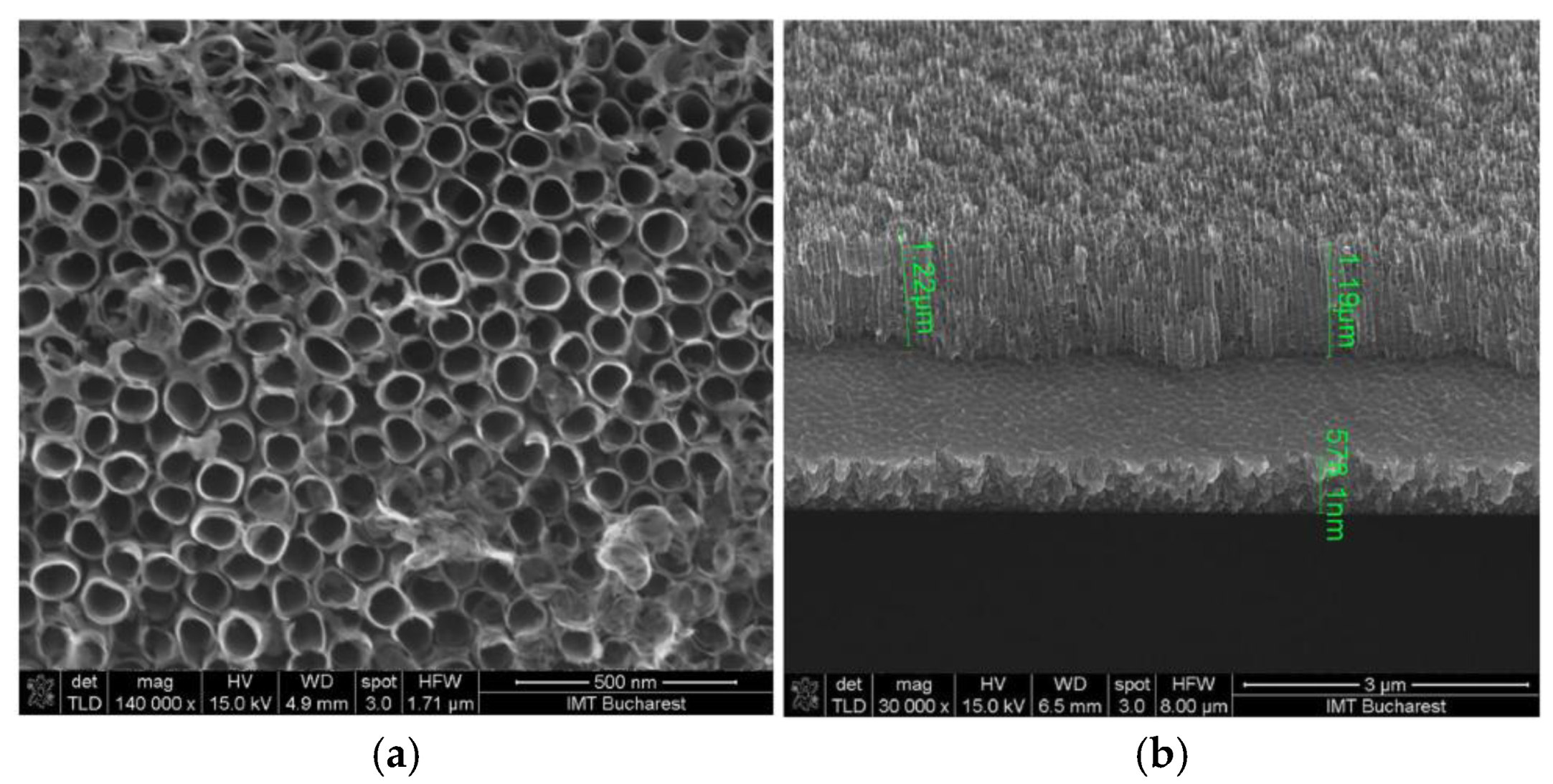
Figure 17.
(a) Representation of successive bonding between analyte MC-LR to aptamers MCTA and carboxylated MWCNT; (b) Selective interactions between MC-LR and the MCTA attached within FGFET; (c) The fabricated FGFET transistor with 3 terminals - Gate (down), Source (left) and Drain (right contact); (d) SEM details of MCTA-MWCNT nanotubes of 26 nm. (all redrawn with MDPI permission from [98]).
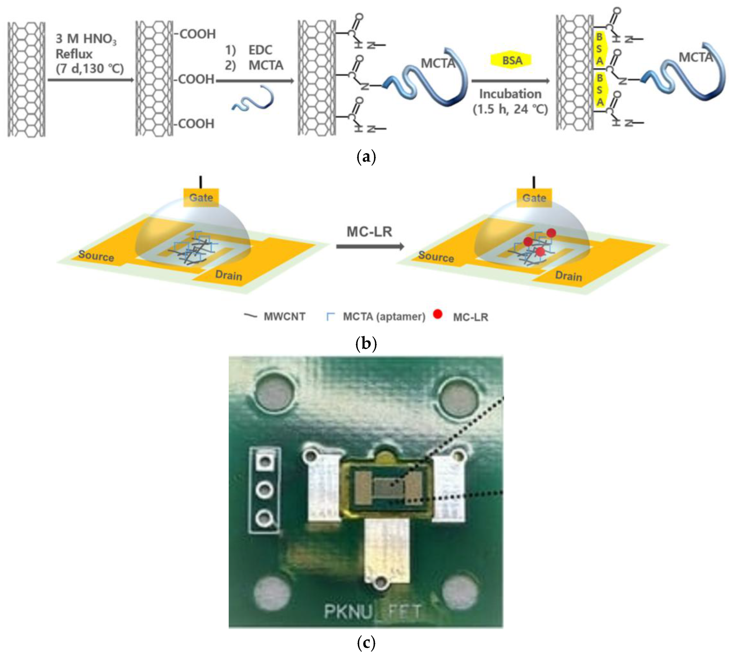
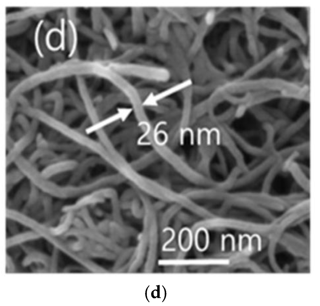
Figure 18.
(a) The schematic of the ISFET with extended gate as sensitive part; (b) the fabricated biosensor; (c) BSA biosensor working with previous ISFET; (d) extraction for the sensitivities emphasize a remarkable super-Nernstian performance for DG configuration. (all redrawn with MDPI permission from [105]).
Disclaimer/Publisher’s Note: The statements, opinions and data contained in all publications are solely those of the individual author(s) and contributor(s) and not of MDPI and/or the editor(s). MDPI and/or the editor(s) disclaim responsibility for any injury to people or property resulting from any ideas, methods, instructions or products referred to in the content. |
© 2025 by the authors. Licensee MDPI, Basel, Switzerland. This article is an open access article distributed under the terms and conditions of the Creative Commons Attribution (CC BY) license (http://creativecommons.org/licenses/by/4.0/).
Copyright: This open access article is published under a Creative Commons CC BY 4.0 license, which permit the free download, distribution, and reuse, provided that the author and preprint are cited in any reuse.


