Submitted:
14 May 2025
Posted:
15 May 2025
You are already at the latest version
Abstract
This paper addresses the critical challenge of time management in wireless sensor networks (WSNs) applied to industrial process control. Although wireless technologies have gained ground in industrial monitoring, their adoption in control applications remains limited due to concerns around reliability and timing accuracy. The study proposes a practical, low-cost solution based on commercial off-the-shelf (COTS) components, leveraging the IEEE 802.15.4-2020 standard in Time Slotted Channel Hopping (TSCH) mode. A custom time management algorithm is developed and implemented on STM32 microcontrollers paired with AT86RF212B transceivers. The proposed system ensures sub-millisecond synchronization drift across nodes by dividing communication into a structured slot frame and implementing precise scheduling and enhanced beacon-based synchronization. Validation is performed through experimental setups monitored with logic analyzers, demonstrating time drift consistently below 600 microseconds. The results confirm the feasibility of using synchronized wireless nodes for real-time industrial control tasks, suggesting that further improvements in hardware precision could enable even tighter synchronization and broader applicability in fast and critical processes.
Keywords:
Wireless Sensor Networks (WSNs)
; industrial process control
; time synchronization
; real-time systems
; embedded systems
; network time management
1. Introduction
Wireless communication is one of the emerging technologies that have been aggressively adopted in the last decade, which allows us to transfer big amounts of data, faster and over much greater distances in real time. Almost every device on the market incorporates at least one wireless technology, whether we are talking about Wi-Fi, Bluetooth or others. Moreover, cost optimization and the emergence of new technologies meant the availability of smart and cheap devices known as the Internet of Things or Industrial Internet of Things for industry. The industrial community has been more reluctant to adopt wireless technologies, especially in process control. Wireless technology is seen as unstable and unpredictable for data transfer in an industrial process. In the past decade, this has gone through a major change with the emergence of the IEEE 802.15.4 [1] standard and its amendments, that allow the secure and efficient transfer of data in an environment where this is critical, such as in an industrial environment.
This standard has led to the development of wireless communication protocols for industrial environments. As examples, we can mention ISA100 Wireless (mostly adopted in the USA) [2] and Wireless HART (mostly adopted in Europe) [3] which mainly allow monitoring of industrial processes. Industrial process control, although it is mentioned in the technical specifications of the two standards, refers to the transmission over wireless of the setpoint rather than the command. Two case studies immediately benefit from this new concept: an industrial process in which the controller and process are at a significant distance from each other, and inside a satellite where one of the methods of reducing production costs and sending it into space is to reduce the number of wires between equipment. Replacing wired control with wireless is not an easy task, considering the industrial process requirements that need to be followed. One of the most important and critical of these requirements is the management of wireless network time, the focus of this article.
Wireless sensor networks (WSNs) have been extensively studied for industrial applications, with a growing focus on synchronization and energy efficiency. [4] provided early insights into the requirements for control-oriented WSNs, highlighting reliability and timing as key barriers to broader adoption. Recent surveys and implementations have reinforced these priorities. For instance, Aponte-Luis et al. [5] showed how IEEE 802.15.4 can support robust industrial monitoring, while Phan and Kim [6] proposed hybrid synchronization schemes scalable to large sensor fields. Moreover, Liu et al. [7] explored architectural trade-offs in synchronization algorithms, including distributed and hybrid approaches, which informed the design choices behind our low-drift, COTS-compatible system.
This article follows a more pragmatic and practical approach by using COTS components and development boards to simulate a time synchronized control loop between two wireless nodes, one being the controller and the other being the process. The starting point was the implementation of the IEEE 802.15.4-2020 standard in Time Slotted Channel Hopping (TSCH) mode which we slightly extended to allow the proper time management in the wireless control network. Promising results have been obtained that point out what is still needed to achieve better time management and allow control over wireless of even faster and more critical processes.
2. Materials and Methods
This section describes the hardware, software, and protocol-level elements used to implement and validate a custom time management algorithm for industrial wireless sensor networks (IWSNs). The system architecture is based on COTS STM32 microcontrollers and AT86RF212B transceivers, configured to operate in IEEE 802.15.4 TSCH mode. A slot frame structure with 10 millisecond timeslots was designed, allowing synchronized communication between wireless nodes using enhanced beacon frames for time alignment. Hardware-level time tracking was implemented using external 32.768 kHz crystals with ±20 ppm tolerance. Development and debugging were conducted in STM32CubeIDE, using CMSIS-compliant C code and a custom hardware abstraction layer (HAL) for microcontroller and transceiver control. System validation was performed with a logic analyzer to measure synchronization drift, confirming sub-millisecond accuracy.
2.1. IEEE 802.15.4
The use of wireless technologies in industrial process control is a novelty, most communication protocols in the industrial field and not only, are used for monitoring: reading the process parameters and sending them to a central unit for display. Both Wireless HART and ISA100 Wireless rely on time management for the proper operation of the wireless network. As they implement only the physical layer from IEEE 802.15.4 standard and rely on proprietary implementations of the upper layers, they define their own time management algorithms. Having this in mind, we had to refer to IEEE 802.15.4 as a starting point in the definition and implementation of a simple and reliable time management algorithm.
Since its first release back in 2003, the IEEE 802.15.4 standard has been continuously amended, adding new modulations, operating frequencies, data rates and application layer features. The standard defines multiple operating modes from which TSCH is the most appropriate for wireless process control as it implies accurate time synchronization between the wireless nodes associated to a network. The concept is simple: it divides time into a sequence of timeslots of fixed intervals that the nodes must follow. Each timeslot allows for one transmission – a command or data frame, and one reception – an acknowledgement, sent and received by following strict timeslot templates. It is expected that the sequence of timeslots will repeat after a certain amount of time, allowing for the predictability of wireless network behavior. This repeating sequence of timeslots is called a slot frame.
Our approach is to use the standard frames as they are defined by IEEE 802.15.4 (beacon, command, data and acknowledgement), and make use of the available payload fields in the extended beacon and acknowledgement frames to send additional data between the nodes. TSCH will be used as the operating mode with a standard slot frame structure used for node management but also for process control.
Having a look at the default IEEE 802.15.4 frame structure, shown in Table 1 alongside the airtime for each field together with the modulation (O-QPSK) and data rate (250 kbps) we aim to use, we have decided to set the timeslot time to 10 milliseconds. This allows us to send and then receive two frames that have the maximum allowable length of 127 bytes, which together with the Preamble, SFD and PHR total up to a maximum of 4.256 milliseconds of airtime per frame. As the acknowledgement frame, which is sent as a reply to a command or data frame, usually has its length much less than 127 bytes, the timeslot time of 10 milliseconds is more than enough to handle the communication between two nodes.
2.2. Hardware
The hardware used to implement and validate time management in the wireless network features the STM32L4 family of microcontrollers [8] from STMicroelectronics and the ATZB-212B-PRO extension board [9] from Microchip, built around the AT86RF212B transceiver. Both components are well known for the abundance of features they provide alongside ease of operation and low power consumption. The wireless node acting as the master clock or the time source is comprised of a pair of development bords: the NUCLEO-L432KC [10] coupled to the ATZB-212B-PRO which runs the implementation of the physical and data link layers and, the NUCLEO-L476RG [11] which runs the application layer as defined by IEEE 802.15.4. The two wireless nodes, which will be part of the control loop, are comprised of the NUCLEO-L152RE [12] development board coupled to an ATZB-212B-PRO extension to maintain consistency. In terms of time keeping, the NUCLEO-L432KC features a 32768 Hz crystal from NDK, part no. NX3215SA-32.768K-STD-MUA-14, with a 20-ppm frequency tolerance and, the NUCLEO-L152RE features a 32768 Hz crystal from Abracon, part no. ABS25-32.768KHZ-6-T, with the same 20 ppm frequency tolerance. Each development board is connected to the PC using USB cables the power the board but also implements a virtual serial (COM) port that is used to log messages placed throughout the code to verify it performs as expected and signal the user when the application reaches a certain state.
A Logic 8 logic analyzer from Saleae was used to monitor microcontroller pins used for debugging. We have used two pins on each board to generate a pulse when the group of timeslots starts and when a timeslot starts. We could therefore measure the time drift between two wireless nodes.
2.3. Development environment
All development has been done in C by using the default development environment from STMicroelectronics, the latest version of STM32CubeIDE [13] which at the time writing this article was 1.18.1. The projects were created as blanks to which we added the header and startup files for the microcontrollers provided by the manufacturer, and which follow the Common Microcontroller Software Interface Standard (CMSIS) [14]. The code is stored in a private GitLab instance serving as a version control system to keep track of all code changes. Live debugging has been done by using the development boards’ built-in ST-Link debuggers to validate the implementation.
3. Results
3.1. Hardware abstraction layer
Optimizing the code execution time and having consistency in this execution requires quick and easy access to the microcontroller’s registers. To do his, we have skipped using the open-source libraries available from the manufacturer (i.e., STM32Cube MCU Packages) and developed a hardware abstraction layer (HAL) to access the most common microcontroller modules like the clock system, the GPIOs, the timers, the communication interfaces, the flash, and ADCs and DACs. The HAL defines standard function headers with the implementation varying from one microcontroller to another and allows for an easy code porting to another hardware platform if needed. The application layer calls these standard functions to configure and use the physical layer of the microcontroller.
The HAL uses the device descriptions to access the microcontroller registers that follow the Common Microcontroller Software Interface Standard (CMSIS) which is an Arm-maintained, vendor-independent software framework that standardizes how code, tools and device descriptions interact with Arm Cortex-based microcontrollers. The goal is to let the user focus on the application instead of relearning low-level details for every new microcontroller. Each module has its registers part of a structure as the one given below as for example, the GPIO module. CMSIS has all microcontroller registers defined as volatile and using the standard C99 data types for interoperability.
typedef struct
{
__IO uint32_t MODER; /*!< GPIO port mode register, Address offset: 0x00 */
__IO uint32_t OTYPER; /*!< GPIO port output type register, Address offset: 0x04 */
__IO uint32_t OSPEEDR; /*!< GPIO port output speed register, Address offset: 0x08 */
__IO uint32_t PUPDR; /*!< GPIO port pull-up/pull-down register, Address offset: 0x0C */
__IO uint32_t IDR; /*!< GPIO port input data register, Address offset: 0x10 */
__IO uint32_t ODR; /*!< GPIO port output data register, Address offset: 0x14 */
__IO uint32_t BSRR; /*!< GPIO port bit set/reset register, Address offset: 0x18 */
__IO uint32_t LCKR; /*!< GPIO port configuration lock register, Address offset: 0x1C */
__IO uint32_t AFR[2]; /*!< GPIO alternate function registers, Address offset: 0x20-0x24 */
__IO uint32_t BRR; /*!< GPIO Bit Reset register, Address offset: 0x28 */
__IO uint32_t ASCR; /*!< GPIO analog switch control register, Address offset: 0x2C */
} GPIO_TypeDef;
Each microcontroller module is then defined as a pointer to a structure that points to the module’s fixed RAM address, as for example the first GPIO module named GPIOA: #define GPIOA ((GPIO_TypeDef *) GPIOA_BASE), with GPIOA_BASE being defined as the base address for the module. Using this structure, we have defined functions to configure and access the functionality of each module. The example given below sets the state for a microcontroller pin, given as the function parameters (port and pin) controlled by a GPIO module and uses the same standard data types as the ones used by CMSIS. The code also follows the MISRA C [15] coding guidelines to make safety- and security-critical embedded software safe, secure, portable and reliable, and is annotated according to Doxygen [16] which can be used to automatically generate code documentation.
/**************************************************************************************************
* @author Andrei Rusu
* @brief GPIO port/pin write
* @param[in] p_ucModule - the GPIO module (e.g. HAL_GPIO_0)
* @param[in] p_ucPin - the GPIO pin (e.g. HAL_GPIO_PIN_0)
* @param[in] p_ucState - the GPIO state (e.g. HAL_GPIO_LOW)
* @remarks
**************************************************************************************************/
void HAL_GPIO_Write(uint8_t p_ucModule, uint8_t p_ucPin, uint8_t p_ucState)
{
switch (p_ucState)
{
case HAL_GPIO_LOW:
{
g_apstHAL_GPIO[p_ucModule]->BSRR = (uint32_t) (1 << (p_ucPin) << 16);
break;
}
case HAL_GPIO_HIGH:
{
g_apstHAL_GPIO[p_ucModule]->BSRR = (uint32_t) (1 << p_ucPin);
break;
}
case HAL_GPIO_TOGGLE:
{
g_apstHAL_GPIO[p_ucModule]->ODR ^= (uint32_t) (1 << p_ucPin);
break;
}
case HAL_GPIO_PULSE:
{
g_apstHAL_GPIO[p_ucModule]->ODR ^= (uint32_t) (1 << p_ucPin);
g_apstHAL_GPIO[p_ucModule]->ODR ^= (uint32_t) (1 << p_ucPin);
break;
}
default: break;
}
}
CMSIS also uses a standard way to define the register bits. This is also adopted in the device definition files available from the manufacturer. As an example, we have listed below a section of the bit definitions for the GPIO_MODER register.
/****************** Bits definition for GPIO_MODER register *****************/
#define GPIO_MODER_MODE0_Pos (0U)
#define GPIO_MODER_MODE0_Msk (0x3UL << GPIO_MODER_MODE0_Pos) /*!< 0x00000003 */
#define GPIO_MODER_MODE0 GPIO_MODER_MODE0_Msk
#define GPIO_MODER_MODE0_0 (0x1UL << GPIO_MODER_MODE0_Pos) /*!< 0x00000001 */
#define GPIO_MODER_MODE0_1 (0x2UL << GPIO_MODER_MODE0_Pos) /*!< 0x00000002 */
The HAL can be made available as source and header files or can be packed in a binary library for easy maintenance and giving the user access just to the header files to call the functions. As a library, it can be easily used in new projects simplifying the overall project structure. We have also defined an intermediate layer between the physical and application layers to configure the microcontroller modules and populate the module interrupt callback functions, which avoids adding application layer code in the HAL files.
3.2. Transceiver driver
To maintain consistency throughout the software project in terms of register access, we have followed the CMSIS guidelines also for the transceiver driver. This meant putting in place the bit definitions for each transceiver register, like the ones available for the microcontroller. As an example, we have listed below a part of the bit definitions for the TRX_CTRL_0 register defining the clock rate for the CLKM pin.
/****************** Address definition for TRX_CTRL_0 register *******************/
#define TRX_CTRL_0 0x03
/****************** Bit definition for TRX_CTRL_0 register *******************/
#define TRX_CTRL_0_CLKM_CTRL_Pos (0U)
#define TRX_CTRL_0_CLKM_CTRL_Msk (0x7UL << TRX_CTRL_0_IRQ_POLARITY_Pos)
#define TRX_CTRL_0_CLKM_CTRL TRX_CTRL_0_IRQ_POLARITY_Msk
#define TRX_CTRL_0_CLKM_CTRL_NO_CLOCK (0x0UL << TRX_CTRL_0_IRQ_POLARITY_Pos)
#define TRX_CTRL_0_CLKM_CTRL_1MHz (0x1UL << TRX_CTRL_0_IRQ_POLARITY_Pos)
#define TRX_CTRL_0_CLKM_CTRL_2MHz (0x2UL << TRX_CTRL_0_IRQ_POLARITY_Pos)
#define TRX_CTRL_0_CLKM_CTRL_4MHz (0x3UL << TRX_CTRL_0_IRQ_POLARITY_Pos)
#define TRX_CTRL_0_CLKM_CTRL_8MHz (0x4UL << TRX_CTRL_0_IRQ_POLARITY_Pos)
#define TRX_CTRL_0_CLKM_CTRL_16MHz (0x5UL << TRX_CTRL_0_IRQ_POLARITY_Pos)
#define TRX_CTRL_0_CLKM_CTRL_250kHz (0x6UL << TRX_CTRL_0_IRQ_POLARITY_Pos)
#define TRX_CTRL_0_CLKM_CTRL_IEEE_802_15_4 (0x7UL << TRX_CTRL_0_IRQ_POLARITY_Pos)
Functions were then defined and implemented to access the transceiver’s features like reading and writing registers, reading frames from and writing frames to the internal FIFO, setting the transceiver in different states (idle, transmission and reception) and using the internal AES module to encrypt data.
3.3. Division of time
The overall aim of the time management algorithm is to achieve a sub-millisecond time drift between any two nodes associated to the wireless network. Why is this needed? If we look at classic control loop, sending a delayed command will cause instability in the controlled process, especially in fast ones. Furthermore, keeping this time drift is in line with the timeslot template defined by IEEE 802.15.4 when using the TSCH operating mode. Considering the COTS development boards used in this experiment and the ±20ppm frequency drift on-board crystals we have fixed the slot frame at 6000 timeslots of 10 milliseconds each leading to a 1-minute-long slot frame. This will lead to a theoretical maximum time drift less than 40ppm x 6000 slots = 2.4 milliseconds per slot frame, assuming one oscillator drifts forward and the other backward. To achieve a sub-millisecond drift between any two nodes, we have concluded to divide the slot frame into groups of 50 timeslots as shown in Figure 1.
Figure 1.
The group of timeslots.
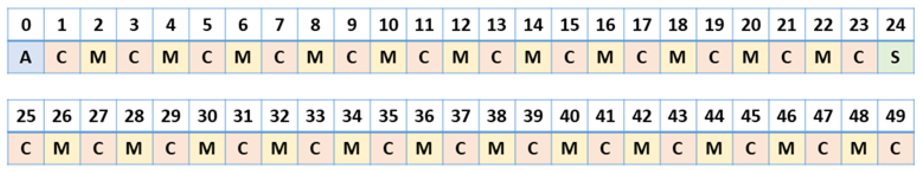
Figure 2.
The timeslot template.
The first timeslot in the group of 50, or timeslot 0 marked with A, is an advertisement timeslot. During this timeslot, the network coordinator (the clock source) sends a beacon frame over the wireless network to notify other wireless devices of the network’s presence. The beacon frame also includes information about the exact time when the coordinator transmitted the frame. Odd timeslots are control timeslots, marked with C, used in control loops to transmit data frames containing commands and process output measurements. Even timeslots are management timeslots, marked with M, used by the coordinator to pass settings to wireless devices, as well as by wireless devices to pass data to the coordinator. Shared timeslots, marked with S, are used by all wireless nodes participating in the network to transmit frames when they do not yet have assigned timeslots. These timeslots are used in procedures such as associating a wireless device with the network, where the last step is to allocate dedicated timeslots. The 25th timeslot in the group of 50 will always be the shared timeslot. In a slot frame, there are 120 advertisement timeslots, 2760 management timeslots, 3000 control timeslots, and 120 shared timeslots.
We have chosen to send an enhanced beacon frame as defined by IEEE 802.15.4, during the advertisement timeslot as it allows the insertion of user payload. This 5-byte payload contains information related to the current network coordinator time: the UTC time in seconds and the time fraction – the timeslot group number, from 0 to 119. As the enhanced beacon frame is being sent during the advertisement timeslot at the moment specified in the timeslot template, a device joining or joined to the network knows the precise absolute time at which the enhanced beacon frame was sent.
3.4. Time synchronization
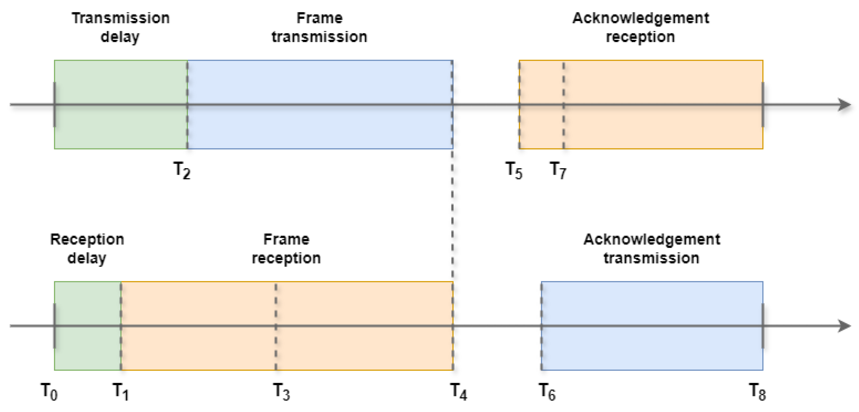
The IEEE 802.15.4 standard defines a timing template (macTimeslotTemplate) that must be followed by every transmission and reception over wireless. Figure 14 illustrates a two-way communication between two wireless devices, the first being the initiator of communication.
A timeslot is defined as the interval between T0 and T8, with a standard duration of 10 milliseconds. According to the transmission template, the actual data frame transmission commences at T2, which, as per the standard, is 2120 microseconds from the start of the timeslot. To ensure correct reception, the second wireless device will enter reception mode earlier, specifically at T1, which is 1020 microseconds from the beginning of the timeslot. The device will then wait for the interval between T3 and T1 for the transmission to begin, i.e., 2200 microseconds. The moment T4 signals the completion of the data frame’s transmission/reception. Subsequently, the receiving device will send an acknowledgment frame to the transmitting device exactly after T6 - T4, which is 1000 microseconds. The first device will enter reception mode at T5 and wait for the acknowledgment frame’s transmission until T7. The end of the transmit/receive process for the acknowledgment frame and the conclusion of bidirectional communication are marked by T8.
Strict adherence to the transmission and reception pattern is essential for the proper functioning of the wireless network, particularly in the time synchronization between wireless nodes. Time synchronization occurs between the network coordinator, which acts as the time source, and each wireless node associated with the network. For this purpose, the enhanced beacon frame is used, which the coordinator transmits in the first timeslot of the group of 50 timeslots. Figure 15 illustrates a synchronization procedure between two wireless nodes, with the top one being the network coordinator and the bottom one being a wireless node that is associated with or joining the network.
Figure 3.
The synchronization procedure
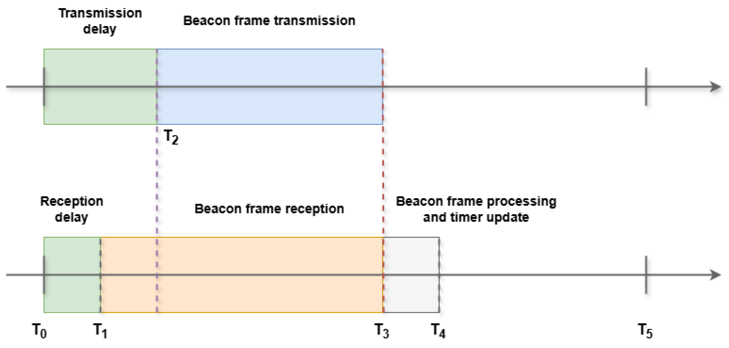
At time T1, the wireless device enters receive mode and awaits the transmission of the beacon data frame. At time T2, in accordance with the transmit and receive template, the coordinator initiates the transmission of the enhanced beacon frame. By time T3, the coordinator has completed the transmission, and concurrently, the wireless device completes its reception of the frame. Subsequently, the device processes the frame by extracting time-related information, including the slot frame, the time and the specific fraction of time when the transmission started. At time T4, the wireless device updates its timeslot and timeslot group timers. Consequently, at time T5, the wireless device will generate an interrupt to indicate the commencement of the next timeslot, thereby maintaining synchronization with the network coordinator.
Synchronization precision remains a key challenge in WSNs. [17] demonstrated how hardware-assisted timestamping and drift correction can enhance accuracy with inexpensive hardware. Similarly, the LPSS protocol [18] achieves energy-efficient scheduling and synchronization by minimizing communication overhead and allocating distinct sync slots to reference nodes. In [19] they also proposed a lightweight approach (SA-MAC) that reduces sync-related traffic. Our work builds on these by integrating deterministic time division with beacon-based alignment and minimal protocol overhead.
3.5. Testing and validation
Testing and validation of the time management has been done by using four development boards from STMicroelectronics: a) the NUCLEO-L476RG implementing the network coordinator application layer, connected via UART to a NUCLEO-L432KC implementing the network coordinator data link and physical layer. The ATZB-212B-PRO extension board featuring the AT86RF212B transceiver is connected to the NUCLEO-L432KC development board via a SPI interface and several pins used for interrupt management, reset and setting the transceiver in low power mode; b) two NUCLEO-L152RE development boards paired to the same ATZB-212B-PRO extension board, implementing the application, data link and physical layers of the wireless nodes. The user starts the network by using an application running on a PC which sends commands to the NUCLEO-L476RG using UART. A diagram of the setup is featured in Figure 4 alongside the actual setup.
Two pins on each of the NUCLEO-L432KC boards part of the wireless nodes were used as debug pins to signal the user via pulses the start of the group of timeslots and the start of each timeslot. The pins were then monitored using the logic analyzer to calculate the time drift between the two nodes. The user interface of the logic analyzer shown in Figure 5 displays 4 channels: Channel 0 monitors the start of each timeslot group and Channel 1 monitors the start of each timeslot for the first wireless node, with Channel 2 and Channel 3 doing the same for the second wireless node.
We have then measured the time drift between the nodes using pairs of markers attached to each two close pulses monitored by Channel 0 and Channel 1, for 1 minute after the devices kept running for more than 1 hour. The measurements are displayed in Figure 6 below showing the time drift is kept below 600 microseconds.
4. Discussion
Industrial control applications demand a blend of precision, low energy usage, and system simplicity. [20] emphasized that synchronization protocols must scale while remaining robust under real-world noise and traffic. [21] recently addressed these challenges through a mesh-star hybrid protocol that balances sync precision with low traffic load. Meanwhile, [22] showed that TDMA-based inter-cluster scheduling significantly reduces delay and jitter in large deployments. These insights support the rationale behind our design: a structured yet flexible timing model based on TSCH and beacon scheduling.
The paper details a simple time management algorithm that can easily be implemented for management the time in a wireless network used for process control. This approach can be used to manage time on wireless nodes based on COTS modules and components allowing also for a decent time synchronization and drift between them. This was achieved by optimizing the code execution time on the microcontrollers by defining and using a HAL that directly accesses the microcontroller registers. This also allows for a good and consistent estimation of the code execution time used later in establishing the timeslot time. As we used different microcontroller families (i.e., STM32L1 and STM32L4) which have many similarities but also differences, the HAL allowed us to easily move the code between one microcontroller to another with only minor changes. The same approach can be used if we would ever need to move the code to, for example, high performance microcontroller families like the STM32F7.
Divion of time has been performed considering the timeslot duration set to 10 milliseconds which is enough time to send and receive two IEEE 802.15.4 frames with the maximum length of 127 bytes for O-QPSK modulation and a 250-kbps date rate. For future implementations using different modulations and/or faster data rates like, for example, UWB modulation that allows up to a 27 Mbps data rate, the timeslot duration can be decreased or increased as needed. Based on the 10-millisecond timeslot, we have defined a 6000-timeslot slot frame that repeats itself continuously. This was also chosen to limit the maximum time drift between any two wireless nodes using COTS components to below 1 millisecond. Using custom made hardware with more precise oscillators will allow the decrease of the slot frame duration resulting in faster node response times. Shorter slot frames also have a smaller footprint on the network coordinator internal memory. Custom hardware can have an impact on the number of timeslots in the timeslot groups and the structure of these timeslot groups as beacon frames do not need to be sent so often. The proposed slot frame structure allows both the operation of control loops and sending of data like sensor data between wireless nodes. This slot frame structure can be adjusted according to the application needs.
Time synchronization, critical in process control applications, has been implemented based on a customized algorithm defined by IEEE 802.15.4. This algorithm uses the timeslot template to send frames at specific times within the timeslot, the timeslot group number and the code execution time within the microcontroller needed to process an incoming frame. This simple approach led to reasonable results in terms of time drift between nodes considering the hardware it is implemented on. Custom hardware with more precise oscillators can lead to even lower time drifts between nodes requiring less frequent needs for time synchronization.
Security and robustness in synchronization have become increasingly relevant in industrial WSNs. Wang et al. [23] proposed a Sybil-resistant protocol that uses node identification and timestamp correlation to filter malicious messages. [7] introduced trust-based synchronization that leverages skew uniqueness to verify message authenticity. These protocols aim to ensure that synchronization sources are trustworthy, a consideration that could be integrated into our beacon validation process for enhanced reliability in hostile environments. Adaptive schemes such as MBATS [24] use mobile beacons to synchronize nodes in environments where fixed infrastructure is impractical or cost prohibitive. Though well-suited for dynamic or mobile networks, such methods introduce complexities not aligned with our static, process-oriented deployment. However, the principle of dynamic sync intervals is relevant for optimizing future enhancements to our fixed-schedule design. While our approach focuses on static industrial deployments, existing research demonstrates value in scenario-specific designs. For example, MBATS adapts to changing sync requirements via mobile beacon mobility, while STSS [25] minimizes beacon collision in overlapping clusters. STOC [25] and related approaches manage sync load but reduce active slot time, affecting throughput. Our use of grouped timeslots and enhanced beacons preserves bandwidth while ensuring tight synchronization, especially useful for control applications with feedback constraints. Liu et al. [26] point to a critical need for scalable protocols that maintain synchronization under variable topologies and high node counts. Our current design is optimized for small to medium industrial cells but lays the groundwork for hierarchical coordination mechanisms needed in future large-scale systems.
Author Contributions
Conceptualization, A.R. and P.D.; methodology, A.R. and P.D.; software, A.R., M.H. and R.M.; validation, A.R., P.D., M.H. and R.M; formal analysis, P.D.; investigation, A.R., P.D., M.H. and R.M; resources, A.R. and M.H.; data curation, A.R. and P.D.; writing—original draft preparation, A.R.; writing—review and editing, A.R., M.H. and R.M.; visualization, A.R. and P.D.; supervision, P.D.; project administration, P.D. All authors have read and agreed to the published version of the manuscript.
Funding
This research received no external funding.
Data Availability Statement
Data used as the baseline for this research can be requested from the authors.
Conflicts of Interest
The authors declare no conflicts of interest.
Abbreviations
The following abbreviations are used in this manuscript:
| WSN | Wireless Senor Network |
| TSCH | Time-Slotted Channel Hopping |
| COTS | Commercial Off The Shelf |
| O-QPSK | Offset Quadrature Phase Shift Keying |
| MBATS | Mobile Beacon-based Adaptive Time Synchronization |
| TDMA | Time Division Multiple Access |
| STSS | Simple Time Shift Scheme |
| LPSS | Low Power Scheduling for Synchronization |
References
- IEEE Std 802.15.4-2020, IEEE Standard for Low-Rate Wireless Networks. 2020.
- ISA100 Wireless Compliance Institute Available online: https://isa100wci.org/ (accessed on 14 May 2025).
- WirelessHART | FieldComm Group Available online: https://www.fieldcommgroup.org/technologies/wirelesshart (accessed on 14 May 2025).
- Zhao, G. Wireless Sensor Networks for Industrial Process Monitoring and Control: A Survey. NPA 2011, 3, 46–63. [CrossRef]
- Aponte-Luis, J.; Gómez-Galán, J.; Gómez-Bravo, F.; Sánchez-Raya, M.; Alcina-Espigado, J.; Teixido-Rovira, P. An Efficient Wireless Sensor Network for Industrial Monitoring and Control. Sensors 2018, 18, 182. [CrossRef]
- Phan, L.-A.; Kim, T. Hybrid Time Synchronization Protocol for Large-Scale Wireless Sensor Networks. Journal of King Saud University - Computer and Information Sciences 2022, 34, 10423–10433. [CrossRef]
- Liu, C.; Pang, H.; Cao, N. Research on Time Synchronization Technology of Wireless Sensor Network. In Proceedings of the 2017 International Conference on Cyber-Enabled Distributed Computing and Knowledge Discovery (CyberC); IEEE: Nanjing, October 2017; pp. 391–394.
- STM32L4 - ARM Cortex-M4 Ultra-Low-Power MCUs - STMicroelectronics Available online: https://www.st.com/en/microcontrollers-microprocessors/stm32l4-series.html (accessed on 14 May 2025).
- AT86RF212B ZIGBIT XPLAINED PRO EXTENSION | Microchip Technology Available online: https://www.microchip.com/en-us/development-tool/atzb-212b-xpro (accessed on 14 May 2025).
- NUCLEO-L432KC | Product - STMicroelectronics Available online: https://www.st.com/en/evaluation-tools/nucleo-l432kc.html (accessed on 14 May 2025).
- NUCLEO-L476RG | Product - STMicroelectronics Available online: https://www.st.com/en/evaluation-tools/nucleo-l476rg (accessed on 14 May 2025).
- NUCLEO-L152RE | Product - STMicroelectronics Available online: https://www.st.com/en/evaluation-tools/nucleo-l152re (accessed on 14 May 2025).
- STM32CubeIDE | Product - STMicroelectronics Available online: https://www.st.com/en/development-tools/stm32cubeide.html (accessed on 14 May 2025).
- CMSIS – Arm® Available online: https://www.arm.com/technologies/cmsis (accessed on 14 May 2025).
- MISRA Available online: https://misra.org.uk/ (accessed on 14 May 2025).
- Doxygen Homepage Available online: https://doxygen.nl/ (accessed on 14 May 2025).
- Cho, H.; Kim, J.; Baek, Y. Enhanced Precision Time Synchronization for Wireless Sensor Networks. Sensors 2011, 11, 7625–7643. [CrossRef]
- Elsharief, M.; Abd El-Gawad, M.A.; Kim, H. Low-Power Scheduling for Time Synchronization Protocols in A Wireless Sensor Networks. IEEE Sens. Lett. 2019, 3, 1–4. [CrossRef]
- Zhang, C.; Yang, S.-H. A Lightweight Time Synchronisation for Wireless Sensor Networks. In Proceedings of the 2020 IEEE International Conference on Networking, Sensing and Control (ICNSC); IEEE: Nanjing, China, October 30 2020; pp. 1–6.
- Yoo, S.; Kim, T. Industrial Wireless Sensor Networks: Protocols and Applications. Sensors 2020, 20, 5809. [CrossRef]
- Wang, Z.; Yong, T.; Song, X. Fast and Low-Overhead Time Synchronization for Industrial Wireless Sensor Networks with Mesh-Star Architecture. Sensors 2023, 23, 3792. [CrossRef]
- Golubnichaya, E.Yu.; Likhttsinder, B.Ya. Slot Data Routing in Cluster Wireless Sensor Networks Based on Time Synchronization of Cluster Heads. In Proceedings of the 2018Systems of Signal Synchronization, Generating and Processing in Telecommunications (SYNCHROINFO); IEEE: Minsk, July 2018; pp. 1–5.
- Wang, Z.; Zeng, P.; Kong, L.; Li, D.; Jin, X. Node-Identification-Based Secure Time Synchronization in Industrial Wireless Sensor Networks. Sensors 2018, 18, 2718. [CrossRef]
- He, J.; Xuan, X.; Zhu, N.; Huang, N.; He, P. Mobile Beacon-Based Adaptive Time Synchronization for Wireless Sensor Networks. J Wireless Com Network 2018, 2018, 220. [CrossRef]
- Wong, C.-M. A Novel Beacon Frame Scheduling Algorithm Based on Cluster-Tree IEEE 802.15.4 Wireless Sensor Networks. In Proceedings of the 2012 IEEE International Conference on Communication Systems (ICCS); IEEE: Singapore, Singapore, November 2012; pp. 285–289.
- Liu, Z.; Ma, Q.; Liu, W.; Sheng, V.S.; Zhang, L.; Liu, G. Access Control Model Based on Time Synchronization Trust in Wireless Sensor Networks. Sensors 2018, 18, 2107. [CrossRef]
Figure 4.
(a) The hardware setup diagram; (b) The development boards used for testing and validation.
Figure 4.
(a) The hardware setup diagram; (b) The development boards used for testing and validation.
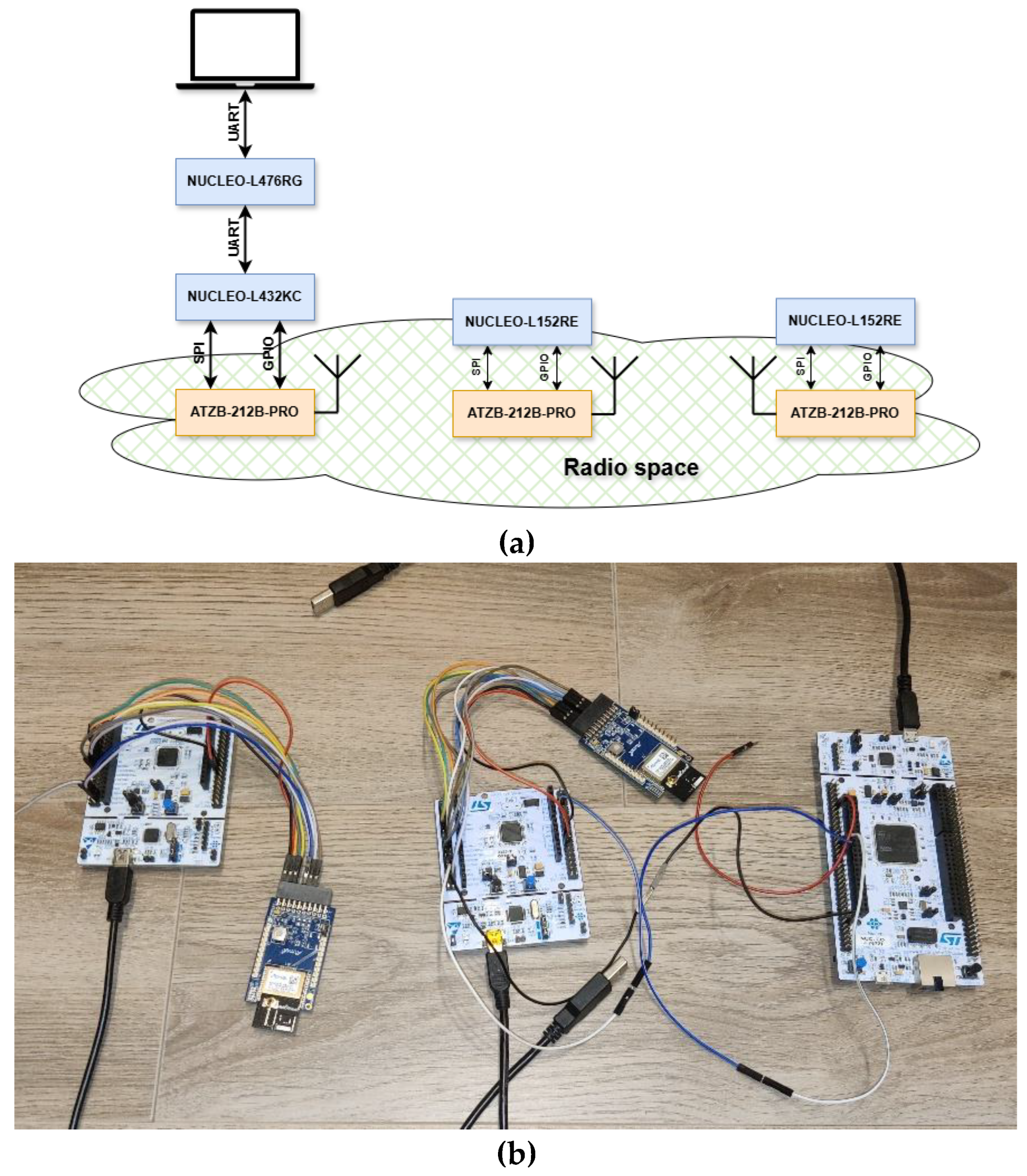
Figure 5.
The logic analyzer UI showing the timeslot group and timeslot pulses.
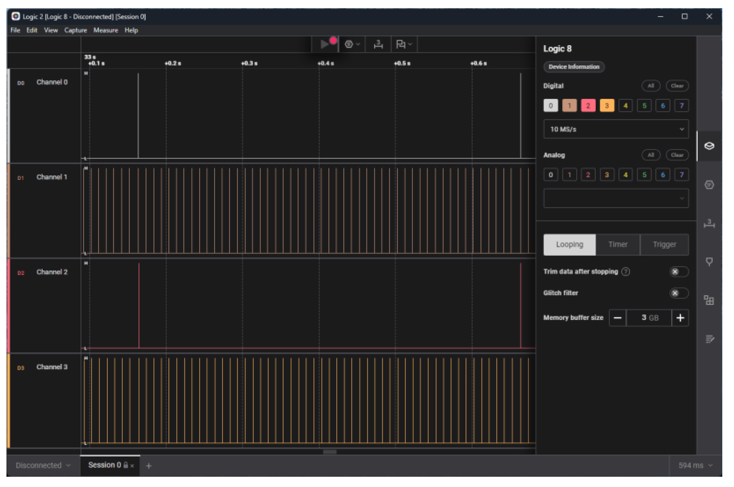
Figure 6.
The logic analyzer UI showing the timeslot group and timeslot pulses.
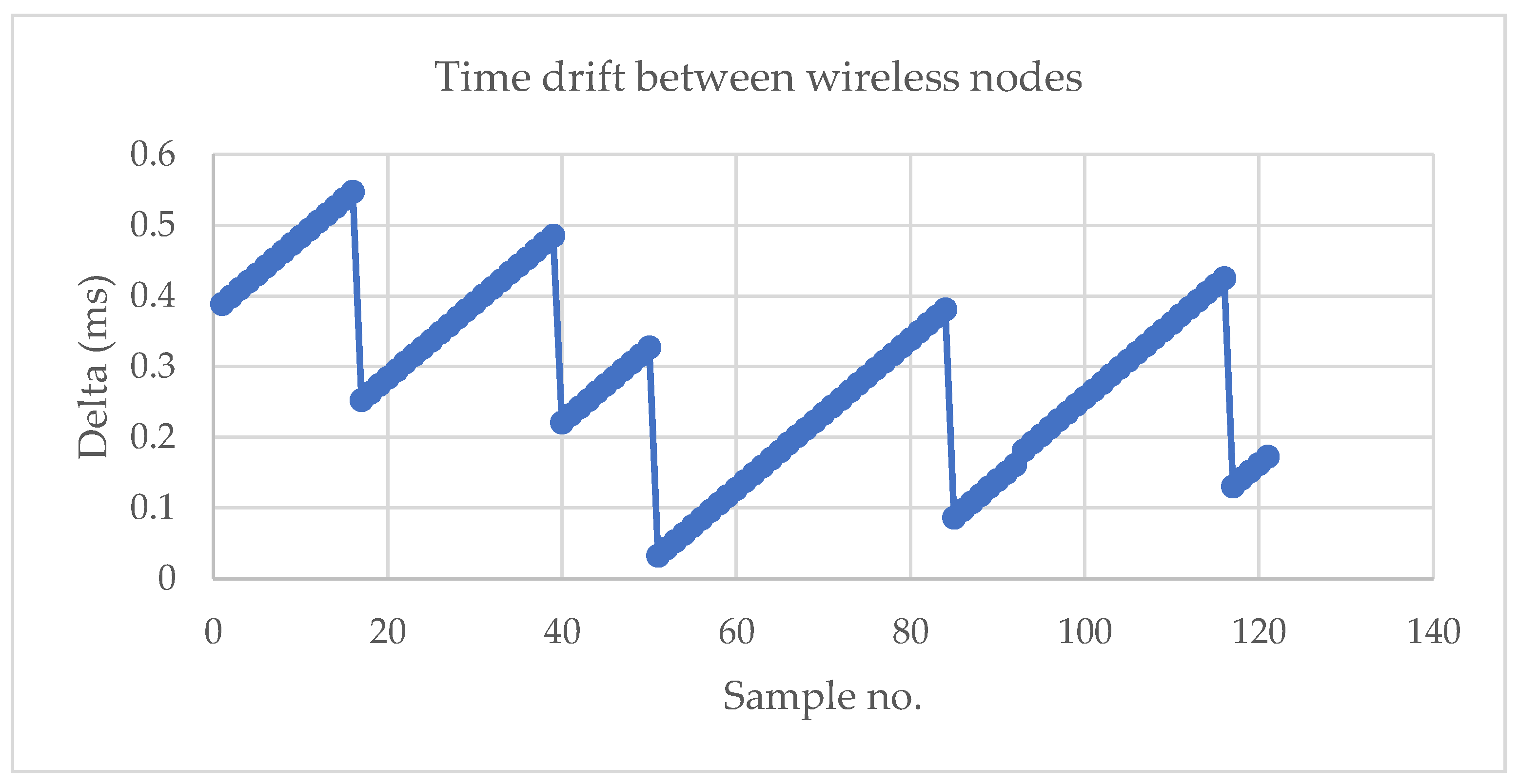

Table 1.
The default IEEE 802.15.4 frame structure and duration.
| Length (bytes) | Value | Duration (µs) | |
|---|---|---|---|
| Preamble | 4 | 0x00000000 | 128 |
| Start Frame Delimiter (SFD) | 1 | 0xA7 | 32 |
| Physical Layer Header (PHR) | 1 | 0x00 ÷ 0x7F | 32 |
| PHY Payload | 127 | various | 32 ÷ 4064 |
Disclaimer/Publisher’s Note: The statements, opinions and data contained in all publications are solely those of the individual author(s) and contributor(s) and not of MDPI and/or the editor(s). MDPI and/or the editor(s) disclaim responsibility for any injury to people or property resulting from any ideas, methods, instructions or products referred to in the content. |
© 2025 by the authors. Licensee MDPI, Basel, Switzerland. This article is an open access article distributed under the terms and conditions of the Creative Commons Attribution (CC BY) license (https://creativecommons.org/licenses/by/4.0/).
Copyright: This open access article is published under a Creative Commons CC BY 4.0 license, which permit the free download, distribution, and reuse, provided that the author and preprint are cited in any reuse.


