Submitted:
14 March 2025
Posted:
17 March 2025
You are already at the latest version
Abstract
Recent advancements in metal/perovskite photodetectors have leveraged plasmonic effects to enhance the efficiency of photogenerated carrier separation. In this work, we present an innovative approach to designing heterostructure photodetectors, integrating a perovskite film with a plasmonic metasurface. Using finite-difference time-domain (FDTD) simulations, we investigate the formation of hybrid photonic-plasmonic modes and examine their quality factors in relation to loss mechanisms. Our results demonstrate that these hybrid modes facilitate strong light confinement within the perovskite layer, with significant intensity enhancement at the metal-perovskite interface—an ideal condition for efficient charge carrier generation. We also propose the use of low-bandgap perovskites for direct infrared passive detection and explore the potential of highly Stokes-shifted perovskites for active detection applications, including ultraviolet and X-ray radiation.
Keywords:
photonics
; plasmonics
; perovskites
; nanostructures
; photodetector
1. Introduction
Metal-semiconductor heterostructures, utilizing Schottky barrier for the photogenerated charge carrier separation, offer many advantages for light detection applications [1,2,3,4], including high-speed operation, broadband response, tunability, design simplicity, and the possibility of on-chip integration. However, they also suffer from strong reflection of incoming light at the metal interface and a narrow depletion region, limiting the efficiency of light absorption and carrier generation. In recent years, metallic nanostructures that support various kinds of plasmonic modes have been explored to address these challenges. Localized surface plasmon resonances (LSPRs), or traveling surface plasmon polaritons (SPPs) excited at the metal/semiconductor interface can produce very tight light confinement that can be utilized to efficiently generate charge carriers both in metal and semiconductor, through internal photoemission (IPE) and electron-hole creation, respectively. In some reports, the enhancement of photodetector responsivity due to plasmonic effects can be greater than one order of magnitude [5]. The reported plasmon-enhanced junctions typically use n- or p-type Si with plasmonic metal contact such as Au, Ag, or Al [1,5,6,7]. Several works have explored the potential of two-dimensional materials, including graphene or transition metal chalcogenides, for the improved junction performance [2,3,8]. As a potential alternative to Si, some researchers attempted to use halide perovskites, including MAPbI3 [9] or [10]. In many aspects, perovskite materials show optoelectronic properties superior to those of Si, especially where tunable bandgap, high absorption coefficients, active operation scheme, and mechanical flexibility are desired. In active devices, the perovskites offer advantages due to their very good emission properties in visible or infrared, and high refractive index values. Also, convenient processing techniques can be used for making perovskite-based nanostructures or nanocomposites, that can be tailored for specific emission characteristics, or emission improvement through the effects such as Purcell enhancement [11,12] and nonlinearity [13].
Schottky-type photodetectors with plasmonic enhancement have been designed either in free-space operation mode [6,14], responding to external light signal, or utilizing integrated optical architectures based on the waveguiding mechanism [15,16]. In case of the free-space operation, coupling of the incident light to plasmonic modes usually requires the presence of one- or two-dimensional grating with subwavelength dimensions, as to increase the in-plane wavevector. In case of waveguided light the coupling operation is more straightforward and can be achieved with simple planar geometry. In this work we introduce novel design approach to metal-semiconductor photodetectors, based on the guided propagation of hybrid plasmonic-photonic modes in a perovskite thin film coupled to plasmonic metasurface. The guided modes can be excited either in passive scheme, through scattering of the external light beam on the plasmonic nanoarray, or through active operation, leveraging perovskite photoluminescence. The metasurface geometry is designed to produce strong field localization in the near infrared wavelengths around 1000 nm (f= 300 THz), however the spectrum of detection can be tuned to shorter wavelengths by utilizing active waveguide operation of the perovskite film. The advantage of using hybrid modes is that they can produce strong field enhancement at the metal/perovskite interface, while at the same time the light absorbed at greater distance from the interface might also contribute to the detected signal, through energy sharing between photonic and plasmonic components. The presented study utilizes finite-difference time-domain (FDTD) simulations to explore the characteristics of the proposed heterostructures, including band dispersion diagrams, mode profiles and the influence of material absorption. Finite structures with dimensions up to m are also considered, to examine the intensity enhancement in what can represent a single detector pixel.
2. Design of the Hybrid Metasurface
The initial study takes into consideration an array of silver nanopillars inside a thin film overlay with thickness 300nm and refractive index 2 on a bulk glass substrate. The pillars are arranged in a square lattice with spatial period a and they are characterized by radius r and height d. The presence of pillars results in periodic modulation of the overlay thickness, which leads to the formation of guided Bloch modes with characteristic frequency and in-plane wave vector . The modulation strength depends on the ratio of pillar height and overlay thickness which we set to 0.3. In addition to the Bloch modes traveling in the overlay (we refer to these modes as photonic), the nanopillars support surface lattice resonances (SLRs), resulting from far-field coupling of the individual LSPRs [17] that are closely confined at the pillar surface. In case of significant overlap between the photonic and plasmonic modes, provided symmetry and polarization match, the modes will experience interference, which manifests itself by avoided crossing of the two bands in band dispersion diagram [18]. Assuming infinite dimensions of the structure, we model the band dispersion and mode profiles with FDTD simulation and the results are presented in the Figure 1. At this stage, for simplicity and clear observation of the mode behavior, the overlay is considered lossless and the pillars are isolated from each other (Figure 1a). The geometric parameters 400 nm, 90 nm, 90 nm and 300 nm were chosen to observe the crossing near 300 THz, with a large value of close to the corner of the Brillouin zone M. As shown in Figure 1b, away from the crossing the modes have a predominant photonic or plasmonic characteristics, however near the intersection they become coupled, giving rise to hybrid modes, with significant contribution of both plasmonic and photonic parts. Due to coupling, the energy stored in such a mode is not bound to the photonic or plasmonic part, but can be transferred between them in time, as has been previously shown on the basis of coupled mode theory for plasmonic resonators integrated in waveguide structures [19,20]. This fact is particularly interesting in the context of designing plasmonic Schottky junctions for the purpose of light detection, where the dominant part of charge carriers is generated through absorption in a thin depletion region. SLR features will be responsible for enhancing the field intensity at this region, while it can be sustained for a longer time, because of the interaction with coupled photonic mode.
For practical implementation of the above concept in designing the photodetector junction, the pillars should be interconnected with a thin silver patch, acting as electrical contact and the overlay must be made of semiconducting material. The 2 refractive index may correspond to various kinds of perovskite materials, which can have different optoelectronic properties, including absorption, emission and carrier mobility. This study focuses mostly on optical behavior of the structures, and so the overlay material is simply characterized by n and (see Section 4 for a more comprehensive discussion on specific materials and applications). The top electrode of the junction can be made of thin metal, transparent conductive oxides, polymers, or composite materials, such as transparent electrodes based on silver nanowires. Also, it can uniformly cover the overlay upper surface or can be positioned on the sides. In the presented FDTD simulations the top electrode is not included, as it does not play a significant role to the demonstrated effects. Figure 2 shows the schematic design and the mode dispersion diagram of the proposed plasmonic-photonic heterostructure. In the guided region (below the light line), at the frequencies 280-300 THz, one can identify two modes which exhibit hybrid plasmonic-photonic character and they dominate the band structure in the specified frequency range. The marked zone on the band diagram is analogical to the crossing sketched in Figure 1, however the presence of silver patch makes the band configuration more complex due to the formation of additional SPP modes. The demonstrated characteristics of the heterostructure implicate that 280-300 THz radiation with a high enough will most favorably couple to the hybrid modes and this can be exploited to manage the optoelectronic properties of the junction.
3. Field Confinement and Influence of Loss
The above findings are then verified by simulating the light behavior in structures with finite dimensions. Figure 3a compares the magnitude of electric field resulting from local excitation of the junction with designed metasurface architecture and reference planar architecture. Within the chosen spectral range 270-310 THz we find an average intensity enhancement near the metal/perovskite interface as factor 3.6, with the enhancement spectrum showing maxima up to =5 at frequencies 286 THz and 307 THz (Figure 3b). In addition to spatial field confinement, one observes the temporal confinement manifested by prolonged decay of electric field (Figure 3c). Excitation source is switched off at = 120 fs, however the electric field recorded in a simulation is sustained until = 400 fs. The temporal confinement results from the excitation of hybrid modes with low group velocity number (as observed in the simulated band structure, Figure 2b). The in-plane propagation and out-of-plane radiation from the structure are also examined in the simulation. The ratio of optical power guided inside the overlay to the total power emitted has maxima that correspond to peaks. As the wave propagates, the power is decreased due to absorption and radiation losses. In current analysis we keep extinction coefficient of the overlay =0, so all absorption is caused by the presence of silver. It is the reason for the loss of power in the low-frequency band of . In contrast, the high frequency band is both absorbed and partially coupled to free-space radiation, as observed in optical power ratio radiated outside of the structure . This implies that the high-frequency peak corresponds to formation of leaky modes, and such modes can be observed in the computed band diagram at smaller wavevector numbers, near the central point .
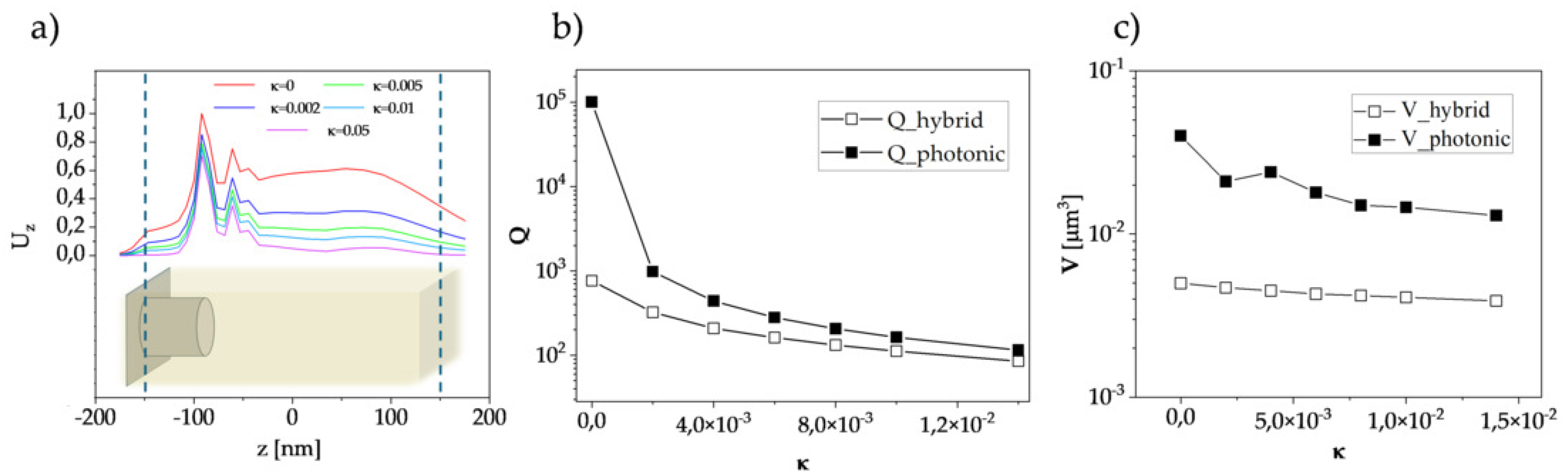
To better understand the potential of designed heterostructure in real applications we also introduce the nonzero extinction coefficient of the overlay material and examine its significance to the formation of hybrid modes. Figure 4a shows the computed energy density carried by a mode as function of vertical coordinate z and integrated over the coordinates and frequency f:
where , are electric and magnetic field magnitudes and , are absolute permittivity and permeability of the overlay material. As expected, big part of the energy is indeed confined near the upper surface of nanopillars due to SLR effects. The contribution of plasmonic and photonic components is balanced at =0, however for nonzero absorption the photonic component is much more affected than the plasmonic one. At =0.05 the energy contribution integrated for z> -70 nm (above the top surface of the nanopillars) drops below 30 %. Despite the fact that material absorption in the overlay can cause considerable loss of energy in the mode, the quality factor of the hybrid modes is less affected by absorption than the quality factor of the reference photonic mode (Figure 4b). Another important factor, mode volume V, also remains quite stable against the material absorption (Figure 4c). The robustness of Q and V, in nonzero absorption case results from the plasmonic component, where the energy loss is already accounted for, by the high number of silver. The Q and V may have crucial meaning when using the designed metasurface for active device operation, as it governs the strength of Purcell enhancement of spontaneous emission in photonic and plasmonic structures.
4. Discussion
There are two major advantages for photodetection process, resulting from photonic and plasmonic nature of the designed metal/perovskite heterostructure. On the one hand, the intensity enhancement at the junction interface, resulting from SLR, will increase the absorption in the depletion zone, which is crucial for generating the photocurrent. Also, this effect will be scaled up by the increased surface area of the junction as compared to planar junction geometry. The effect of increased area on the junction performance have been already studied in the past [21,22]. On the other hand, the photonic component, in the form of guided Bloch mode, might be of no less importance. Although, its direct contribution to the number of photogenerated carriers will not be significant, it will share a portion of its energy with the SLR. Considering, that the device can work in active operation scheme, where the incident light is absorbed in the overlay and re-emited with lower frequency, utilizing the hybrid modes can create the opportunity to scale up the thickness of the device, without sacrificing the plasmonic enhancement in thin depletion zone. In the follow-up to this work, there will be a more specific analysis of energy transfer rate between photonic and plasmonic components and thorough analysis of the device performance in passive and active schemes.
Regarding passive and active operation schemes there are important differences in the design and operation principle of the device. In both cases the absorption of infrared light at the junction interface is responsible for generating charge carriers. However, while the passive device deals with infrared radiation coming from the free space, the active device utilizes the luminescence generated in the overlay. In the first case, coupling of incident light to guided modes of the metasurface can be only achieved through interaction with the nanopillar array, as to match the of incident light and guided mode. This might require tailoring the design of nanopillar array to provide sufficient coupling efficiency and bandwidth. In the latter case, the internal emission of the overlay material will couple to the guided modes more easily. Also, for passive scheme, the overlay should be designed to absorb infrared, however the value of should be kept moderate ( - ) in order to maintain the photonic component. Then, the chosen perovskite could be one with electronic bandgap slightly above 1.24 eV (as results from f = 300 THz). Good candidates to fulfill this criterion could be well recognized solar cell material methylammonium lead iodide () [23] and some of the recently developed tin-iodide or germanium-iodide based perovskites [24,25]. On the contrary, the overlay material used for active operation scheme should be efficient infrared emitter with possibly small self-absorption, which is related to the Stokes shift of the material (spectral shift between absorption and emission bands). Highly Stokes-shifted perovskites with infrared emission can be made through lanthanide doping [26] and they can be used for indirect detection of shorter wavelength visible light, or even X-ray radiation, utilizing the radioluminescence phenomena [27]. Finally, given very broad choice of perovskite compounds and possibility of using convenient solution-based deposition methods, such as spin coating, there is big potential in designing layered structures with multiple absorption bands, which can be used for broadband light detection. This can also involve the combination of passive and active layers for optimizing the absorption at the interface, while maintaining efficient emission in the overlay.
5. Methods
All simulations were conducted using 3D FDTD solver in Ansys Lumerical. Randomly distributed, in-plane oriented dipole sources (dipole cloud) are used for optical excitation of the structure. Bloch boundary conditions in directions and perfectly matched layers (PML) in z direction are used for modelling the mode profiles and band dispersion in infinite structures. Non-uniform mesh size is applied with refinement to 2 nm at the pillar region. A number of randomly distributed time monitors is used for monitoring the decay of electric field, following the excitation. The Q-factors are obtained from the fitting decay curve, using Lumerical built-in functionality. Mode volumes V are computed as the volume where the is greater than . In case of finite structures the Bloch boundary conditions in are replaced with PML.
6. Conclusions
In this work we explore the behavior of hybrid plasmonic-photonic heterostructure and we introduce a new concept of utilizing the hybrid modes to boost the performance of photodetectors based on the metal/semiconductor junction with Schottky barrier. The hybrid modes arise from coupling of the guided Bloch modes propagating in the semiconducting overlay with the SLR modes supported by silver nanopillars. We optimize the design of the junction to achieve enhancement in optical intensity near the frequency of 300 THz. The simulation of 4×4 m pixel with the designed nanostructure shows intensity enhancement up to 5 times, as compared to planar junction design. We also investigate the effect of material absorption on the mode characteristics and we discuss the potential of using perovskite materials for both passive and active types of overlay. The demonstrated results imply that hybrid mode operation of the device can be advantageous for overcoming the thickness limitations in plasmonic Schottky junctions.
Author Contributions
Conceptualization, D.K. and M.D.B.; Investigation, D.K.; Visualization, D.K.; Writing-original draft, D.K; Validation, Y. C. and M.D.B.; Writing-review and editing, Y. C. and M.D.B.; Funding acquisition, M.D.B.
Funding
M.D.B. acknowledges funding from the National Science Center, Poland under grant OPUS-24 no. 2022/47/B/ST5/01966.
Data Availability Statement
The data concerning all the results in this work are not publicly available at this moment but may be obtained from the authors upon request.
Conflicts of Interest
The authors declare no conflict of interest.
References
- Huang, Z.; Mao, Y.; Lin, G.; Yi, X.; Chang, A.; Li, C.; Chen, S.; Huang, W.; Wang, J. Low dark current broadband 360-1650 nm ITO/Ag/n-Si Schottky photodetectors. Opt. Express 2018, 26, 5827–5834. [Google Scholar] [CrossRef] [PubMed]
- Periyanagounder, D.; Gnanasekar, P.; Varadhan, P.; He, J.H.; Kulandaivel, J. High performance, self-powered photodetectors based on a graphene/silicon Schottky junction diode. J. Mater. Chem. C 2018, 6, 9545–9551. [Google Scholar] [CrossRef]
- Gao, W.; Zhang, S.; Zhang, F.; Wen, P.; Zhang, L.; Sun, Y.; Chen, H.; Zheng, Z.; Yang, M.; Luo, D.; et al. 2D WS2 Based Asymmetric Schottky Photodetector with High Performance. Advanced Electronic Materials 2021, 7, 2000964. [Google Scholar] [CrossRef]
- Goykhman, I.; Desiatov, B.; Khurgin, J.; Shappir, J.; Levy, U. Waveguide based compact silicon Schottky photodetector with enhanced responsivity in the telecom spectral band. Opt. Express 2012, 20, 28594–28602. [Google Scholar] [CrossRef]
- Frydendahl, C.; Grajower, M.; Bar-David, J.; Zektzer, R.; Mazurski, N.; Shappir, J.; Levy, U. Giant enhancement of silicon plasmonic shortwave infrared photodetection using nanoscale self-organized metallic films. Optica 2020, 7, 371–379. [Google Scholar] [CrossRef]
- Alavirad, M.; Olivieri, A.; Roy, L.; Berini, P. High-responsivity sub-bandgap hot-hole plasmonic Schottky detectors. Opt. Express 2016, 24, 22544–22554. [Google Scholar] [CrossRef]
- Abubakr, E.; Abadi, A.; Oshita, M.; Saito, S.; Kan, T. Optimizing geometry and metal-dependent performance of Si-based Schottky plasmonic photodetectors. Optical Materials 2024, 150, 115175. [Google Scholar] [CrossRef]
- Levy, U.; Grajower, M.; Gonçalves, P.A.D.; Mortensen, N.A.; Khurgin, J.B. Plasmonic silicon Schottky photodetectors: The physics behind graphene enhanced internal photoemission. APL Photonics 2017, 2, 026103. [Google Scholar] [CrossRef]
- Shahriyari, H.; Hatefi-Kargan, N.; Daraei, A. Plasmonic graphene/perovskite Schottky barrier photodetector. Zeitschrift fur Naturforschung A 2024, 79, 815–821. [Google Scholar] [CrossRef]
- Zeng, L.H.; Chen, Q.M.; Zhang, Z.X.; Wu, D.; Yuan, H.; Li, Y.Y.; Qarony, W.; Lau, S.P.; Luo, L.B.; Tsang, Y.H. Multilayered PdSe2/Perovskite Schottky Junction for Fast, Self-Powered, Polarization-Sensitive, Broadband Photodetectors, and Image Sensor Application. Advanced Science 2019, 6, 1901134. [Google Scholar] [CrossRef]
- Ye, W.; Yong, Z.; Go, M.; Kowal, D.; Maddalena, F.; Tjahjana, L.; Wang, H.; Arramel, A.; Dujardin, C.; Birowosuto, M.D.; et al. The Nanoplasmonic Purcell Effect in Ultrafast and High-Light-Yield Perovskite Scintillators. Advanced Materials 2024, 36, 2309410. [Google Scholar] [CrossRef] [PubMed]
- Makowski, M.; Ye, W.; Kowal, D.; Maddalena, F.; Mahato, S.; Amrillah, Y.T.; Zajac, W.; Witkowski, M.E.; Drozdowski, K.J.; Nathaniel.; et al. Scaling Up Purcell-Enhanced Self-Assembled Nanoplasmonic Perovskite Scintillators into the Bulk Regime, 2024, [arXiv:physics.optics/2411.18477].
- Hardhienata, H.; Ramdhani, I.; Alatas, H.; Faci, S.; Birowosuto, M.D. Investigating the Photovoltaic Performance in ABO3 Structures via the Nonlinear Bond Model for an Arbitrary Incoming Light Polarization. Micromachines 2023, 14. [Google Scholar] [CrossRef] [PubMed]
- Wu, S.; Chen, C.; Dai, Y.; Ye, J.; Xu, X.; Liu, X.; Tian, F.; Xu, Y.; Hu, H. Direct-detected spectroscopy based on a plasmonic Schottky photodetector and a deep neural network. Opt. Lett. 2023, 48, 4965–4968. [Google Scholar] [CrossRef]
- Gosciniak, J.; Atar, F.B.; Corbett, B.; Rasras, M. Plasmonic Schottky photodetector with metal stripe embedded into semiconductor and with a CMOS-compatible titanium nitride. Scientific Reports 2019, 9. Cited by: 50; All Open Access, Gold Open Access, Green Open Access. [Google Scholar] [CrossRef]
- Goykhman, I.; Sassi, U.; Desiatov, B.; Mazurski, N.; Milana, S.; De Fazio, D.; Eiden, A.; Khurgin, J.; Shappir, J.; Levy, U.; et al. On-Chip Integrated, Silicon-Graphene Plasmonic Schottky Photodetector with High Responsivity and Avalanche Photogain. Nano Letters 2016, 16, 3005–3013, Cited by: 276; All Open Access, Green Open Access, Hybrid Gold Open Access. [Google Scholar] [CrossRef]
- Cherqui, C.; Bourgeois, M.R.; Wang, D.; Schatz, G.C. Plasmonic Surface Lattice Resonances: Theory and Computation. Accounts of Chemical Research 2019, 52, 2548–2558. [Google Scholar] [CrossRef]
- Azzam, S.I.; Shalaev, V.M.; Boltasseva, A.; Kildishev, A.V. Formation of Bound States in the Continuum in Hybrid Plasmonic-Photonic Systems. Phys. Rev. Lett. 2018, 121, 253901. [Google Scholar] [CrossRef]
- Tuniz, A.; Song, A.Y.; Della Valle, G.; de Sterke, C.M. Coupled mode theory for plasmonic couplers. Applied Physics Reviews 2024, 11, 021309. [Google Scholar] [CrossRef]
- Chen, C.; Oh, S.H.; Li, M. Coupled-mode theory for plasmonic resonators integrated with silicon waveguides towards mid-infrared spectroscopic sensing. Opt. Express 2020, 28, 2020–2036. [Google Scholar] [CrossRef]
- Wu, Y.; Yan, X.; Zhang, X.; Ren, X. A monolayer graphene/GaAs nanowire array Schottky junction self-powered photodetector. Applied Physics Letters 2016, 109, 183101. [Google Scholar] [CrossRef]
- Wang, B.; Zhang, J.; Lian, S.; Wu, H.; Liu, Z.; Wang, G. Patterned 3D-graphene for self-powered broadband photodetector. Applied Physics Letters 2024, 125, 142103. [Google Scholar] [CrossRef]
- Frolova, L.A.; Davlethanov, A.I.; Dremova, N.N.; Zhidkov, I.; Akbulatov, A.F.; Kurmaev, E.Z.; Aldoshin, S.M.; Stevenson, K.J.; Troshin, P.A. Efficient and Stable MAPbI3-Based Perovskite Solar Cells Using Polyvinylcarbazole Passivation. Journal of Physical Chemistry Letters 2020, 11, 6772–6778. [Google Scholar] [CrossRef] [PubMed]
- Morteza Najarian, A.; Dinic, F.; Chen, H.; Sabatini, R.; Zheng, C.; Lough, A.; Maris, T.; Saidaminov, M.I.; García de Arquer, F.P.; Voznyy, O.; et al. Homomeric chains of intermolecular bonds scaffold octahedral germanium perovskites. Nature 2023, 620, 328–335. [Google Scholar] [CrossRef] [PubMed]
- Singh, J.K.; Mandal, S.K.; Banerjee, G. Refractive index of different perovskite materials. Journal of Materials Research 2021, 36, 1773–1793. [Google Scholar] [CrossRef]
- Dagnall, K.A.; Conley, A.M.; Yoon, L.U.; Rajeev, H.S.; Lee, S.H.; Choi, J.J. Ytterbium-Doped Cesium Lead Chloride Perovskite as an X-ray Scintillator with High Light Yield. ACS Omega 2022, 7, 20968–20974. [Google Scholar] [CrossRef]
- Haposan, T.; Arramel, A.; Maulida, P.Y.D.; Hartati, S.; Afkauni, A.A.; Mahyuddin, M.H.; Zhang, L.; Kowal, D.; Witkowski, M.E.; Drozdowski, K.J.; et al. All-inorganic copper-halide perovskites for large-Stokes shift and ten-nanosecond-emission scintillators. J. Mater. Chem. C 2024, 12, 2398–2409. [Google Scholar] [CrossRef]
Figure 1.
The formation of hybrid plasmonic-photonic modes in thin film of perovskite coupled to array of plasmonic nanopillars. a) Schematic view of hybrid metasurface, and b) its local photonic band structure in the proximity of high symmetry point M (=0.5) with insets showing mode distributions along the higher and lower frequency bands. Dashed lines demonstrate the shape of the uncoupled photonic (red) and plasmonic (blue) bands.
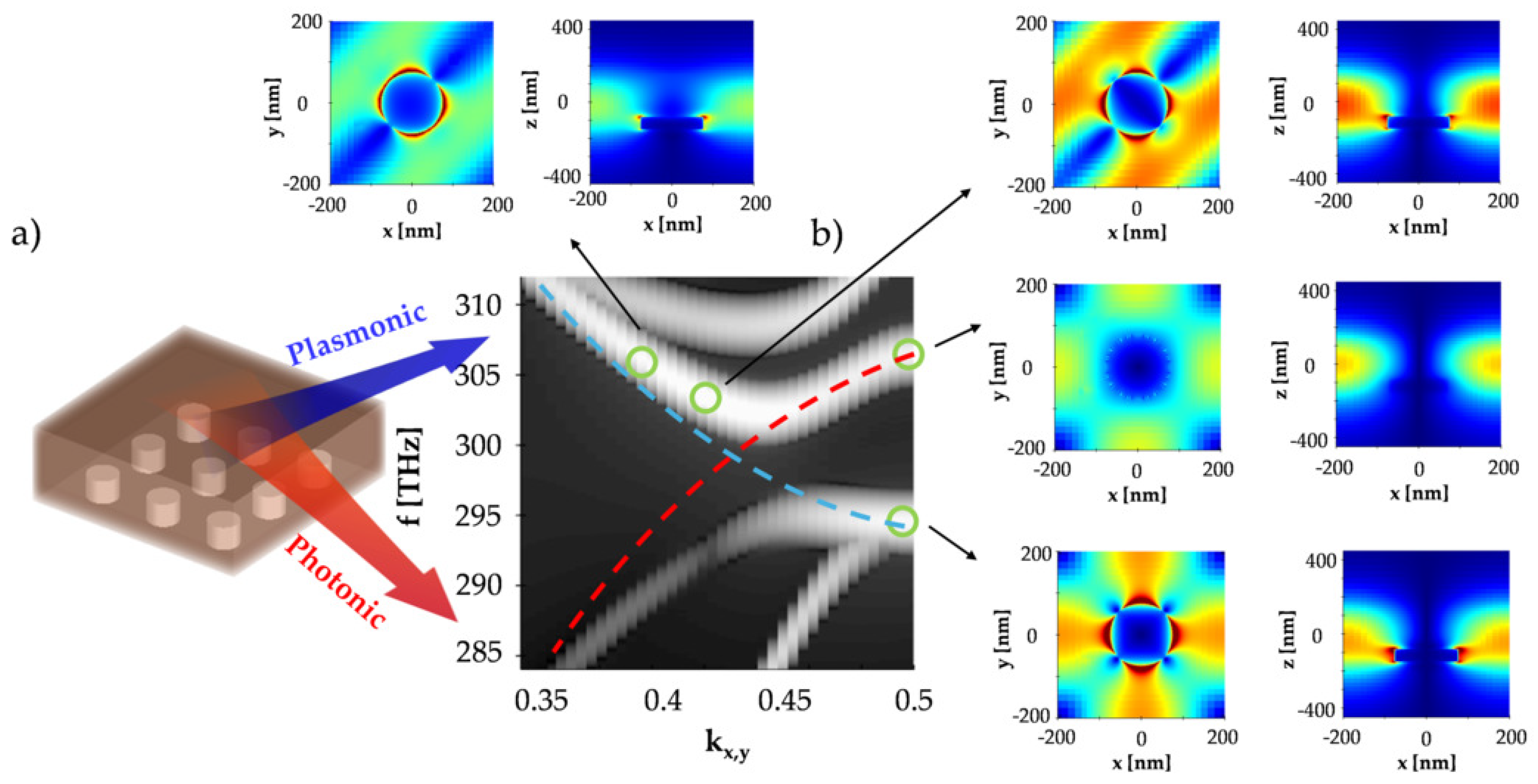
Figure 2.
a) Design of the plasmonic-photonic heterostructure proposed as photodetector and b) the corresponding band structure of the electromagnetic modes supported in it. The orange line represents air line which separates guided and radiative mode regions. The red dashed line marks the mode of interest, which dominates other modes in 290-300 THz frequency range.
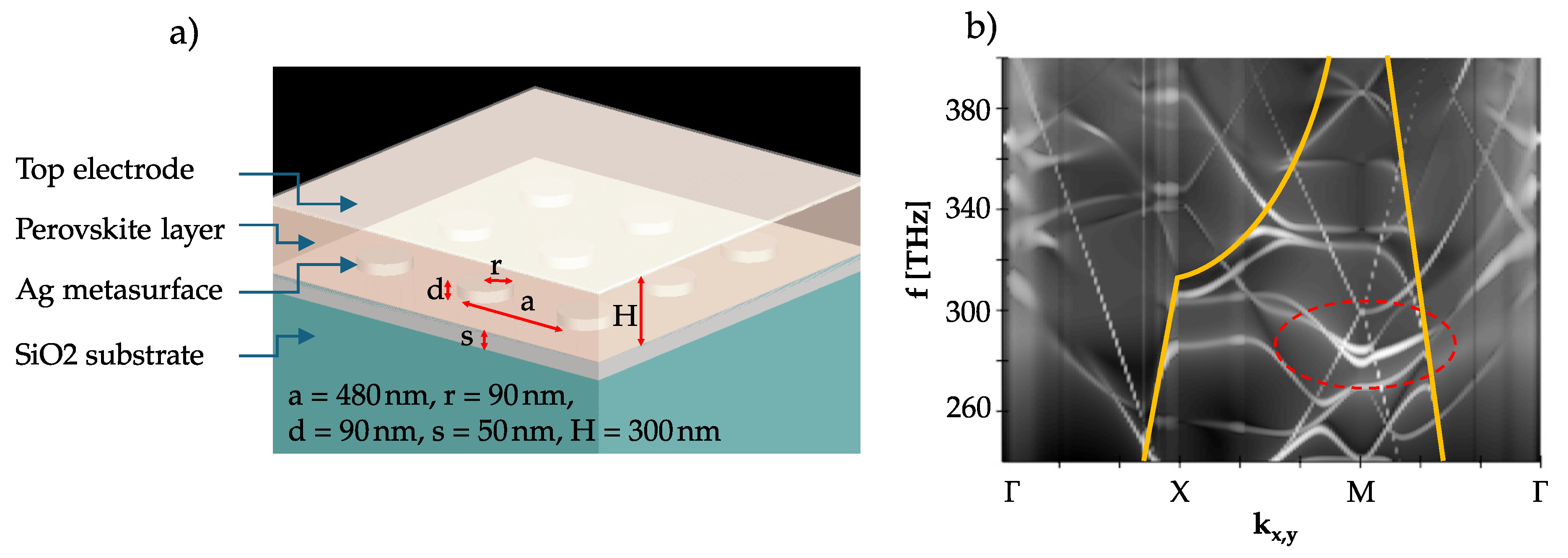
Figure 3.
The demonstration of enhancement in the finite structure. a) Comparison of the electric field magnitude simulated in planar (top) and structured (bottom) junction configuration at vertical coordinate z = 1 nm corresponding to the metal patch and z = 91 nm corresponding to the top of the pillars.
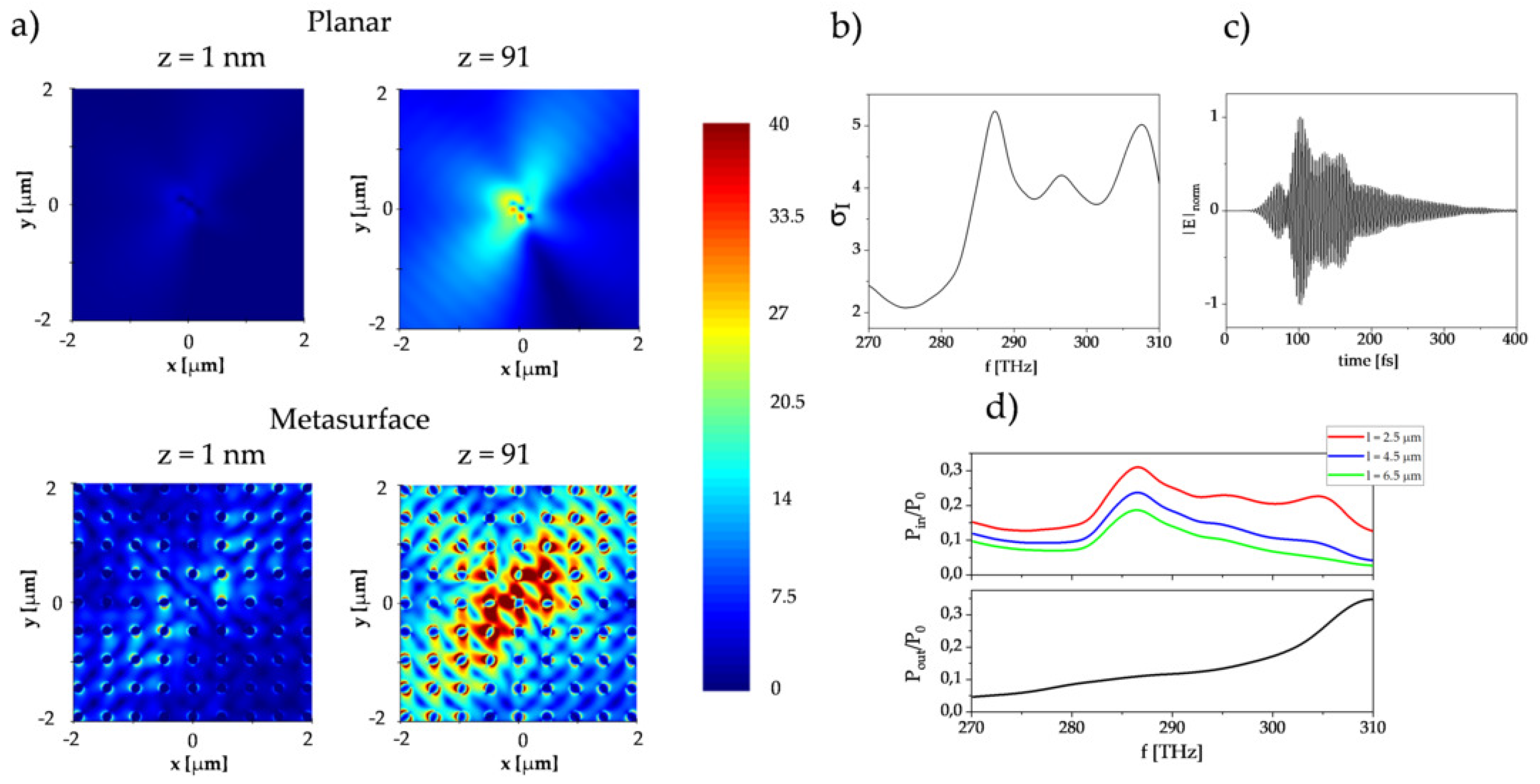
Figure 4.
The effect of material absorption on the characteristics of hybrid modes. a) Simulated electromagnetic energy density along vertical coordinate z in the heterostructure with varying absorption. The drop of the simulated b) quality factor Q and c) mode volume V with material absorption simulated for the hybrid mode and for the reference photonic mode.
Disclaimer/Publisher’s Note: The statements, opinions and data contained in all publications are solely those of the individual author(s) and contributor(s) and not of MDPI and/or the editor(s). MDPI and/or the editor(s) disclaim responsibility for any injury to people or property resulting from any ideas, methods, instructions or products referred to in the content. |
© 2025 by the authors. Licensee MDPI, Basel, Switzerland. This article is an open access article distributed under the terms and conditions of the Creative Commons Attribution (CC BY) license (https://creativecommons.org/licenses/by/4.0/).
Copyright: This open access article is published under a Creative Commons CC BY 4.0 license, which permit the free download, distribution, and reuse, provided that the author and preprint are cited in any reuse.


