Submitted:
05 February 2025
Posted:
05 February 2025
You are already at the latest version
Abstract
The reflectance (R) of linear and circular micro-gratings on c-plane sapphire Al2O3 ablated by a femtosecond (fs) laser, were spectrally characterised for thermal emission ∝ (1 − R) in the mid-to-far infrared (IR) spectral range. An IR camera was used to determine the blackbody radiation temperature from laser patterned regions, which showed (3 − 6)% larger emissivity dependent on the grating pattern. The azimuthal emission curve closely followed the Lambertian angular profile ∝ cos θa at the 7.5-13 µm emission band. The backside ablation method on transparent substrates was employed to prevent debris formation during energy deposition as it applies a forward pressure of > 0.3 GPa to the debris and molten skin layer. The backside ablation maximises energy deposition at the exit interface where the transition occurs from the high-to-low refractive index. Phononic absorption in the Reststrahlen region 20–30 µm can be tailored with the fs-laser inscription of sensor structures/gratings.
Keywords:
femtosecond laser ablation
; direct energy deposition
; radiative cooling
; anti-reflective surfaces
1. Introduction
Fs-laser machining has been a versatile technique for fabricating micro-to-nano-scale patterned surfaces for precise tailoring of optical [1,2], thermal [3], tribological [4,5], and wettability [6,7] properties of different materials’ surfaces from reflective metals [8,9,10] to transparent dielectrics [11,12,13]. Fs-laser fabrication via direct laser writing enables the realisation of metasurfaces—defined as sub-wavelength structures—with featured sizes on the scale of a few micrometers.[9]. This enables a simple prototyping capability for fabricating 2D and 3D patterns, making modifications on mid-to-far IR spectrum and extending even further into the THz spectral range (millimetre scale) [14]. In this range, standard projection lithography approaches are feasible in terms of resolution but they are not highly demanding. However, high-aspect-ratio fabrications become demanding when the depth approaches the wavelength scale (sub-milimetre), e.g., optical vortex generators [15].
The reflectivity of a surface must be controlled for its anti-reflective and highly emissive properties, which can be tailored by fs-laser texturing at IR wavelengths [16,17]. Indeed, the reflectance of a mirror-finished surface will change to due to surface roughness (RMS) [18]. The decrease in R contributes to the increase in absorbance A, which in turn enhances the emissivity E. Therefore, the phenomenon of R reduction has a direct link to radiative cooling applications.
The mid-to-far IR spectral window at the Reststrahlen band, defined between the transverse optical (TO) and longitudinal optical (LO) phonons with energies and , in the energy dispersion (where wavevector ) can be explored for sensor and slow light applications. This is because both real and imaginary parts of the refractive index are very large ( attaining ), especially the found in polar materials. In the spectral regions where , a strong (even near to perfect) absorption condition can be achieved similarly as the strong absorption observed in laser-driven breakdown plasmas. Indeed, when the real part of the permittivity ( is approaching 0 (where permittivity ), the epsilon-near-zero (ENZ) conditions cab be realised, which occurs in perfect absorbers and near-breakdown plasmas ( is the breakdown definition). In Al2O3, ellipsometry measurements at this spectral region were shown to be suitable for determining the permittivity at different surface orientations [19]. The static and high-frequency dielectric constants for the electric E-field perpendicular to the c-axis of Al2O3 (c-plane used in our study) are and , respectively, and they are related to each other via the Lyddane-Sachs-Teller rule . The complex dielectric function (permittivity) at a wavelength of (or cyclic frequency ) comprises contributions from both phonons and electrons, as described by the Drude model. These contributions correspond to the IR region (Reststrahlen band) and the optical spectral regions, respectively. The complex dielectric function is given by [18]:
where the electron plasma frequency is defined by electron density , electron charge e, and its effective mass ; is the free-carrier damping constant determined by the carrier (electron) mobility and , the phonon damping constant. The Reststrahlen bands possess particularly strong absorption resonances (e.g., at the TO band), where the Kramers-Kronig relations dictate that the real permittivity becomes negative over a narrow region. This results in strong phonon-photon interactions, leading to the formation of surface phonon polaritons (SPhPs). The dispersion relation at this region has a typical anti-crossing signature [20]:
One of c-plane sapphire’s pronounced Reststrahlen bands is at the - pair 439–481 [19,21]. In this band, strong reflectivity occurs and was present in our experiments. The Eqn. 2 is useful to define the angle of incidence at which the SPhP can be launched using IR photons. This occurs at the wavevector (k)-matching condition facilitated by an optical element, e.g., a grating with period or a prism. The phase matching conditions for IR photon, SPhP surface wave, and surface grating with period are:
where m is an integer. The phase (momentum) matching conditions Eqn. 3 are also applicable for the extraction of IR (black body) radiation from the TO phonon modes parallel to the surface using the same grating. This was demonstrated on the SiC surface with a grating of m, which corresponded to the conditions and out-coupling angle instead of in Eqn. 3 [22]. Moreover, since the grating was sub-wavelength relative to the emitted IR photons, the emissivity exhibited strong directionality due to coherence, a phenomenon known as Wolf’s effect [23,24]. This effect can be used to enhance IR blackbody emission and holds potential for applications in radiative cooling [22]. The Wolf’s effect is influenced by the depth of the gratings, and the use of circular gratings to facilitate the experimental observation of out-coupled IR light was a key motivation for this study. It was found that the reflectivity increases at 385–388 ( mode) and decreases at 633 , while the modes were smoothed in the spectral reflectivity (R) profile following fs-laser ablation at 1030 nm/280 fs and surface patterning with ablation ripples [25].
Sapphire as a crystal form of Al2O3 which has great thermal, optical, and mechanical properties. Its physical properties such as high thermal conductivity, resistance to thermal stress, and low thermal expansion, make it a reliable material under extreme conditions [26]. Moreover, sapphire is the second hardest material with the ability to withstand high temperatures, which makes it a durable material option for applications demanding high infrared emissivity and radiative cooling. In addition, sapphire has a wide bandgap (>8 eV), which makes it less compatible with conventional photo-assisted machining techniques. Instead, femtosecond laser (fs-laser) ablation as an advanced method shows its advantages in surface texturing where precise structuring and processing are required [27]. By introducing more complex structures, such as thin films with grating patterns that exhibit Fano resonances, the optical response in the Reststrahlen band can be further enhanced. Fano resonances typically arise from the coupling of extended wave systems with compact oscillators, such as dielectric or plasmonic nanoparticles [28,29]. In thin and periodically modulated dielectric films, Fano-like coupling with unbound planar waveguiding modes enables precise control over reflection, transmission, and absorption properties [30]. This controlled light interaction gives rise to sharp resonance features [31], which can be effectively utilised for spectral, polarisation, and spatial filtering, further advancing infrared sensing and photonic applications.
Here we demonstrated the depth control in fs-laser micro-machining of c-plane sapphire Al2O3 to engineer reflectivity bands for enhanced emission in mid-to-far IR and radiative cooling. The depth and aspect-ratio control of surface texturing reduced the reflectance, R, which corresponded to an enhanced absorbance, A which is directly related to the emittance, E. The emittance and use of Wolf’s effect on the IR material enables controlled extraction of radiation tailored to specific IR bands.
2. Experimental: Materials and Methods
2.1. Ablation of Grooves on Sapphire with a Gaussian Beam
A Pharos fs-laser was used for the machining of sapphire chips, with a central wavelength = 515 nm, pulse duration = 230 fs, repetition rate kHz, scanning speed = 15 mm/s, pulse energy up to = 12.5 J (power W), and a numerical aperture i.e. with a focal spot of 1.22/NA ≊ 1.4 m. The number of pulses per focal spot at the constant pulse density mode of 2000 (the pulse-to-pulse spacing m). The laser was focused on the backside of the sapphire chips to reduce the influence of ablation debris and to localise the intensity at the interface between the exit sapphire surface and air.The machining was achieved under the condition of varying fluence per pulse J/ and different number of passes . For each condition, 4 grooves were engraved to calculate the average dimension parameters (width, depth, ablation volume, and aspect ratio) for a more representative result.
After optimising the fabrication conditions, two distinct patterns were produced over a large area, both with a grating period of m and a patterned area diameter of 5 mm. The first pattern consists of concentric circles (CC) forming a grating, while the second features evenly spaced, horizontal lines (HL), arranged within a circular outline. Both patterns were back-side ablated using the fundamental wavelength nm under identical scanning and focusing conditions (see parameter set in the caption of Figure 4) and were subsequently used for emissivity measurements.
2.2. Structural Characterisation
To characterise the dimensions of the machined sapphire grooves, a 3D profile was captured using a Bruker Contour GT-K 3D Optical Profiler at a magnification of . Using the open source software, Gwyddion, the average depth, and width of grooves were calculated. The depth (D) was defined as the distance from the bottom of the groove to the surface plane, and the width (W) was defined as the distance between two edges of the groove. The aspect ratio was defined as the ratio of the previous two quantities () and the ablation volume was defined as a conical pyramid (). The results are presented in Figure 3 The surface morphology was captured using a scanning electron microscopy (SEM). The RAITH 150TWO electron beam lithography writer was used in the in field emission mode using back-scattered electrons. The sapphire samples were coated with 20 nm Cr using a Quorum Q150T ES Plus Spin Coater before SEM imaging.
2.3. Spectral Characterisation
Laboratory-based Fourier transform infrared (FTIR) spectra were measured in both reflection and transmission modes at 2.5–25 m using a Bruker Vertex 70 spectrometer coupled with a Hyperion 1000/2000 FTIR microscope (Bruker Optik GmbH, Ettlingen, Germany). The absorption was then calculated according to Kirchhoff’s law where (scattering is accounted for by reflection and absorption). The measured transmittance, reflectance, and calculated absorptance were plotted as Figure 5.
Synchrotron-based FTIR spectra were also acquired at the Infrared Microspectroscopy (IRM) beamline, Australian Synchrotron (Clayton, Victoria), using a Bruker Vertex 80v spectrometer coupled with a Hyperion 3000 FTIR microscope (Bruker Optik GmbH, Ettlingen, Germany) and a helium-cooled Si:B photodetector. The focal spot was m; a objective lens () and an identical pair of objective lens () were used for reflection and transmission measurements, respectively. All the synchrotron-FTIR spectra were recorded within a spectral range of 4000-–340 using 4 spectral resolution. Blackman-Harris 3-Term apodisation, Mertz phase correction, and a zero-filling factor of 2 were set as default acquisition parameters using the OPUS 8.0 software suite. A non-polarised synchrotron-IR beam was used. The results are presented in Figure 1 with the fabrication conditions specified in the figure caption.
2.4. Thermal Emission
The temperature profiles of the sapphire samples were captured using a thermal imaging camera (Optris PI 160, Germany) which operates in the 7.5-13 m IR band. When the temperature of a hot water tank, made of polypropylene, with a water volume of , becomes stable, the sapphire samples were placed in the centre of the water tank to heat up. As the hot water tank progressively cooled in the ambient room environment, the sapphire samples were cooled as well. The thermal camera was placed directly above the sapphire samples to capture the temperature variations during the heating and cooling phases. A thermal monitoring software (Optris PIX Connect, Germany) was used to connect the camera to the computer and was used to monitor the labelled sample areas.
3. Results and Discussion
3.1. Effect of Orientation and Depth of Ablated Groves on T and R
Determining emittance as absorbance (), requires direct measurements of transmittance T and reflectance R (). Measurements were carried out on laser-ablated gratings with different orientations and depths using the synchrotron radiation (IR beamline at Australian Synchrotron) as shown in Figure 1. To maximise A, R should be minimised. Therefore, to reduce the reflectivity of the material’s surface with refractive index (for light incidence from air with ), a periodic square pattern of sub-wavelength structures with period p and depth h is typically employed [32]. The sub-wavelength pattern should satisfy [33] with the height (the thinnest layer) of the pattern. Reflection is minimised when the refractive index of the anti-reflection coating is the geometric mean of the refractive index on either side of the material . For the laser-patterned surface, the volume fraction of material f and air defines the effective refractive index . This shows how period and depth are both important for the reduction of R (for intensity ) [34]:
where reflections from two interfaces are and (for E-field), respectively, is the refractive index of the substrate/sample, and the phase delay term for the h thickness of the anti-reflection layer.
Figure 1 shows measured R and T spectra at mid-far-IR for gratings with fs-laser ablation on the c-plane of Al2O3 at different orientations and depths m. The dichroic ratio for reflectance parallel and perpendicular to the ablated groves was largest for the deepest grating at (m) which corresponds to the period of the grating.
Strong R modulation is observed at the Reststrahlen band - pair 439–481 (22.8–20.8m) and was strongest for the deepest pattern. Strong dichroism in R and A can be explored for sensor applications of surface-enhanced IR absorption (SEIRAS), which is widely used at shorter IR wavelengths. The benefit of the Reststrahlen region is the possibility to launch SPhP (surface phonon polariton) at the TO-band using a grating of (see dispersion Eqn. 2). In this regime, slow light at large-k is realised with the local electric field enhancements ( is incident field), where intensity follows with . These enhancements can become significantly stronger similar to those observed in the visible spectral range. Polarisation dependence on reflectance R (Figure A1) shows very strong modulation for incidence along and across the linear grating pattern. The grating is acting as an optical element to add momentum to launch SPhP (Eqn. 3)) or to extract IR emission via Wolf’s effect.
3.2. Characterisation of Back-Side Ablation: Threshold, Structure, R, and T Spectra
Figure 2 (a)–(d) shows SEM images of pass laser ablation on sapphire with different fluences 8.43, 12.42, 16.41, 20.40 at the condition pulse overlap per focal diameter. When the fluence was below 12.42 , the surface had structural modifications, however, without clear ablation pits/grooves. At a fluence of 16.41 , clear ablation structures appear on sapphire. By increasing the pulse fluence to 20.40 , material removal at ablation sites becomes deeper, forming a continuous trench. At the same fluence for passes sapphire was ablated with debris coming out of the surface even at the lowest pulse fluence (Figure 2(e–h)). This signifies the presence of a cumulative effect in sapphire ablation. By measuring the ablation depth, width, and calculating the ablation volume versus the cumulative dose, the ablation threshold at different conditions can be estimated as shown in Figure 3(a). Sapphire’s ablation threshold is around 1.6 for pass. It is close to a single pulse ablation threshold of sapphire J/ considering pulse accumulation over the focal spot at the used writing conditions.
Figure 2.
Back-side ablation of Al2O3. SEM images of grooves on sapphire ablated by 515 nm/230 fs/200 kHz Gaussian beam with different pulse fluence and number of passes ; increased from the left to the right ; (a), (b), (c) and (d) show single-pass ablation while (e), (f), (g) and (h) show 20-pass ablation. Focusing with objective lens; the focal spot m; number of pulses per focal diameter is at constant pulse density 2000 . Linear polarisation of the writing beam was aligned with the scan direction (horizontal).
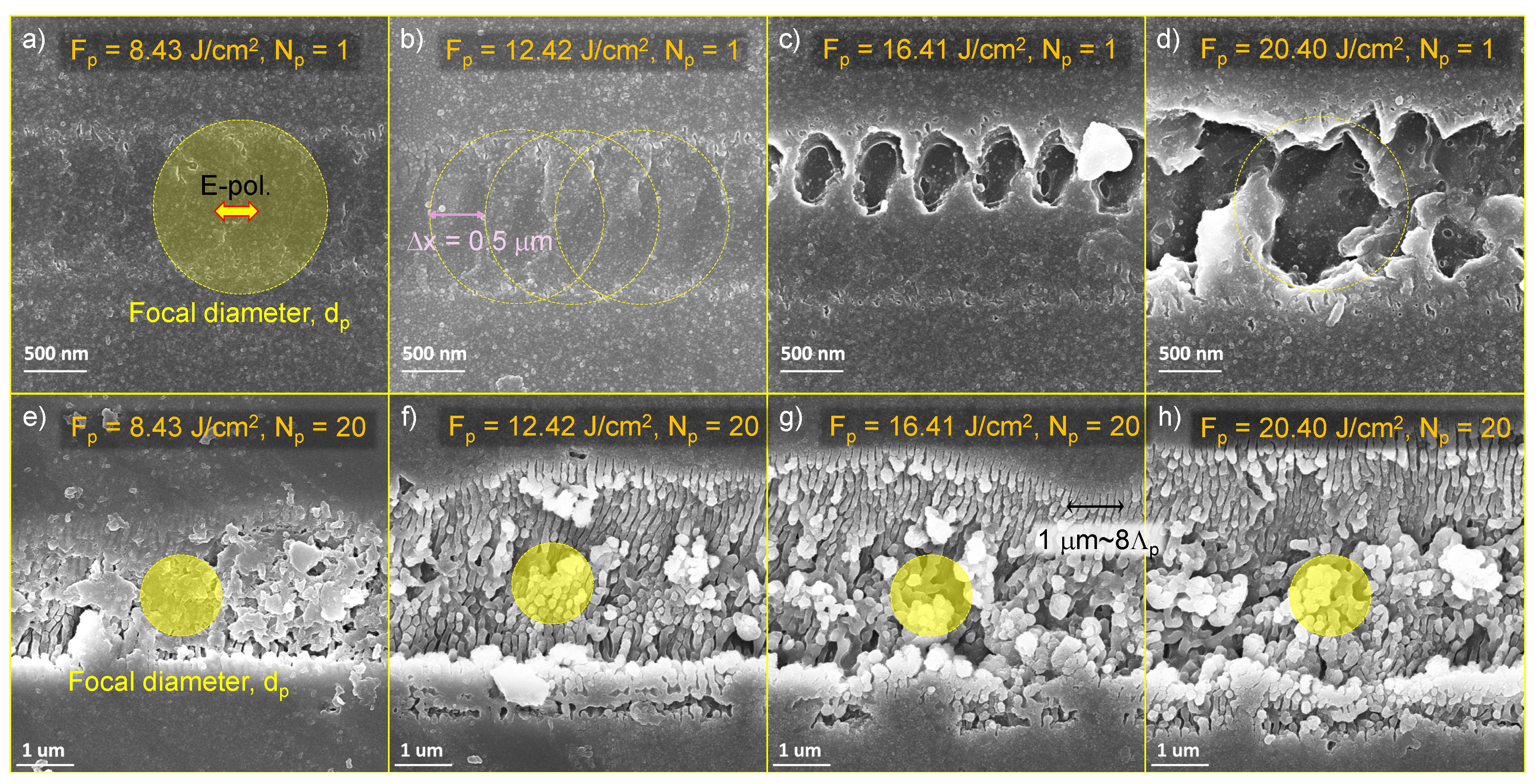
Figure 3.
Back-side ablation of Al2O3. (a) The effective ablation volume and (b) aspect ratio of ablated grooves on sapphire engraved by 515 nm/230 fs/200 kHz Gaussian beam irradiation. The x-axis is the total dose , where is the number of passes. N is the number of pulses per focal spot diameter . The pulse-to-pulse separation was m for the constant pulse density mode of 2000 ) corresponding to , scan speed = 15 mm/s, laser repetition rate f = 200 kHz. The pulse fluence ( pulse energy), the ablation volume (conical pyramid) and the aspect ratio were calculated with W the width and D the depth of the groove; is the coefficient of determination for each linear fitting. Focusing with objective lens; m.
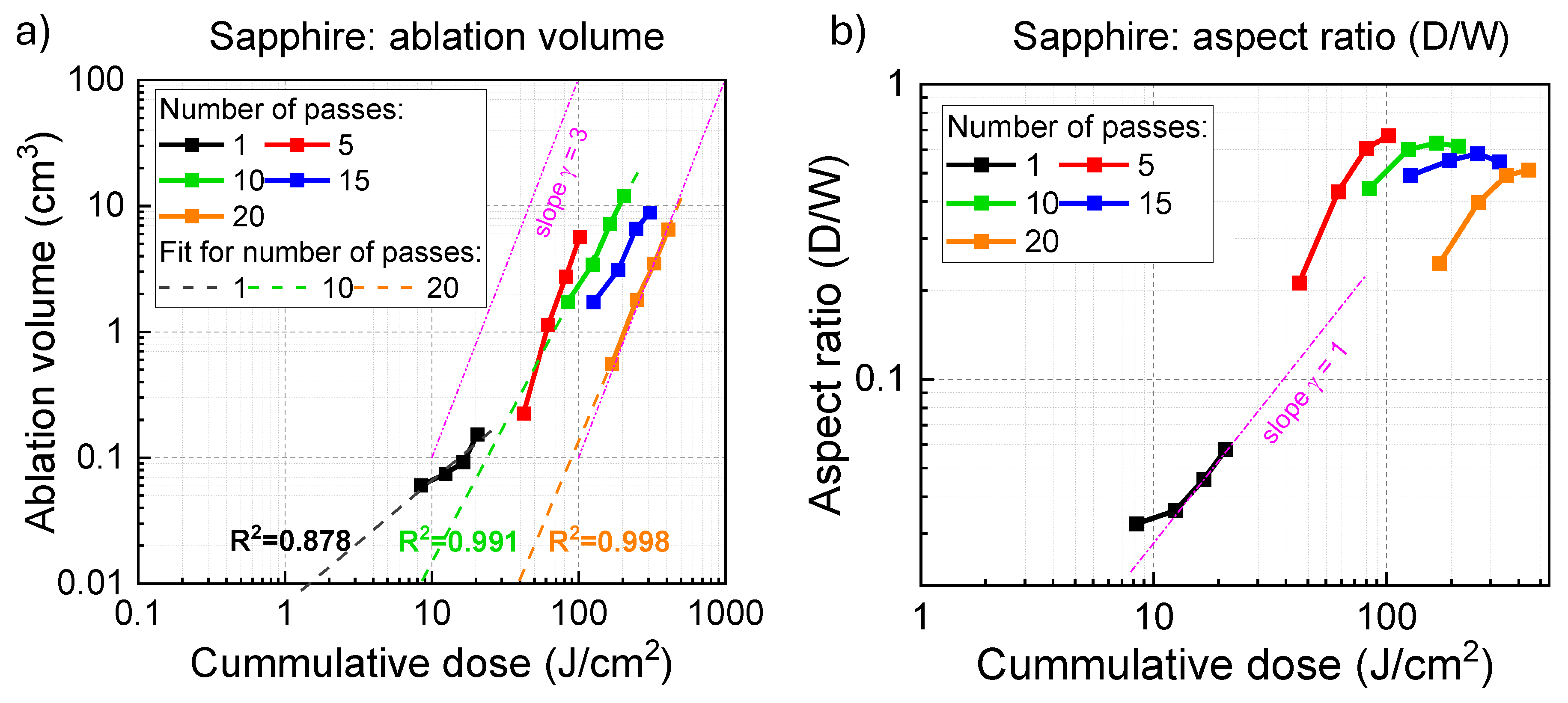
Figure 4.
Back-side ablation of Al2O3. SEM images of large-area pattern fabrication with a diameter of 0.5 cm on sapphire chips ablated by 515 nm/230 fs/200 kHz Gaussian beam, pulse fluence = (pulse average intensity TW/), number of passes = 10. (a) The fabricated area is filled with horizontal hatching (HL). (b) The same fabrication condition for the concentric circle (CC) pattern; both HL and CC patterns have the grating period m; the insets (left-bottom) are optical pictures of the fabricated sapphire chips.
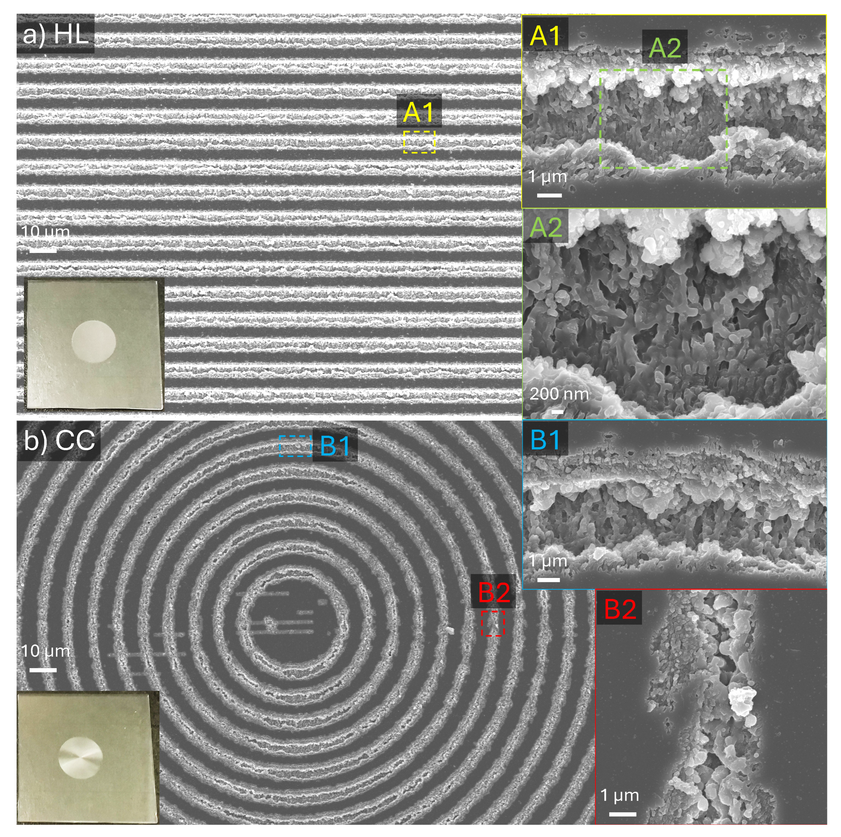
For the back-side ablation, ripples with a period of nm were observed (Figure 2(g)). This period closely matches the expected value for internal ripples, calculated as nm, where the laser wavelength is nm and the refractive index of sapphire is . The observed pattern is typical for normal ripples with grating-like structures perpendicular to the linear polarisation of the electric E-field. Interestingly, surface ripples for the front-side (most usual experimental case) ablation appear once multi-pulse irradiation takes place starting from two pulses overlapped . For the back-side ablation, ripples were prominent only when larger pulse fluence was used, and ablation was larger than the geometrical focal spot and evolved on the side walls of ablation grooves. One possible explanation for the absence of ripples close to the threshold of their formation is, photon pressure. Indeed, the average intensity TW/ (close to the ablation threshold) generates forward pressure along the beam GPa, which facilitates forward ablation of the skin-depth of highly excited and absorbing sapphire at the back-side focus. Moreover, the reflection of the incoming laser beam from the skin region ionised Al2O3 deposits twice the photon momentum (doubles the pressure). The obvious shallow removal of material over exactly the focal spot was discernible by SEM.
The ablated volume follows the power law on the dependence of fluence/dose (Figure 3). This is consistent with two-photon absorption (TPA) in energy deposition. The density of deposited energy depends on the pulse fluence and skin depth , where , is electron density, is the density of critical plasma at the wavelength of irradiation, and A is the absorbance. When electrons are generated by TPA, , the scaling is confirmed in experiments. Once the density of deposited energy (per volume) exceeds the binding and ionisation energy of the material (Al2O3), the ablation starts [35]. The removal of skin depth layers by ablation can explain the experimental data (Figure 3(a)). Figure 3(b) shows the aspect ratio increases with the increase of cumulative deposited dose on the sapphire’s surface. The aspect ratio was increasing linearly with the increase of dose/fluence near the ablation threshold. At repeated scans with a larger cumulative dose, the depth was increasing faster than the width. This is consistent with the Gaussian intensity profile, which decays laterally as while axially (along propagation) as . The depth increase saturates after several scans since the focal spot position was not changed with respect to the ablated depth in consecutive scans.
The large areas were fabricated using the 20.4 Gaussian irradiation with passes on the backside of sapphire, with 0.1 m depth offset per pass during scanning. Figure 4 shows SEM images of 2 patterns at different magnifications, with detailed micro-structure of the groove (A1, B1, B2) and nano-scale ripples (A2). The micro-structure is polarisation-dependent, where ripples were more pronounced when polarisation was perpendicular to the scanning direction. When the laser was scanning along the horizontal direction, and polarisation was vertical, deeper grooves and ripples were formed at the bottom. Laser-ablated patterns affected spectral properties. The HL pattern shows both lower reflectance and transmittance at mid-IR as compared with the CC pattern, leading to higher absorptance. The possible reason is that the HL pattern is deeper. Additionally, more ripple formation in the HL pattern due to the polarisation of fs-laser irradiance largely enhanced surface roughness, promoting broadband absorption in the IR range. This is because fs laser-induced nanostructures amplify absorption by acting as micro-resonators for IR emission [36]. The absorptance at 7-11 m is near to 1 due to a large 0.5-mm-thickness and the strong absorbance of sapphire[37]. Moreover, absorption at 11-19 m was increased from 0.2 to 0.6 with the HL patterning.
Figure 5.
Laboratory-based FTIR spectra of the horizontal line (HL) and concentric circular (CC) grating structures (Figure 4), collected using a Bruker Vertex spectrometer with an internal Globar™ IR source (unpolarised). Experimentally measured reflectance R (normalized to Au mirror) and transmittance T. Then the absorptance A is calculated from the energy conservation . Changes of (measured), and A (calculated) at 7.5-13 m caused emittance changes when imaged by IR camera (Figure 6); highlighted by a rectangular block. A star marker with an arrow shows a tendency of increased A at m as compared with unstructures Al2O3.
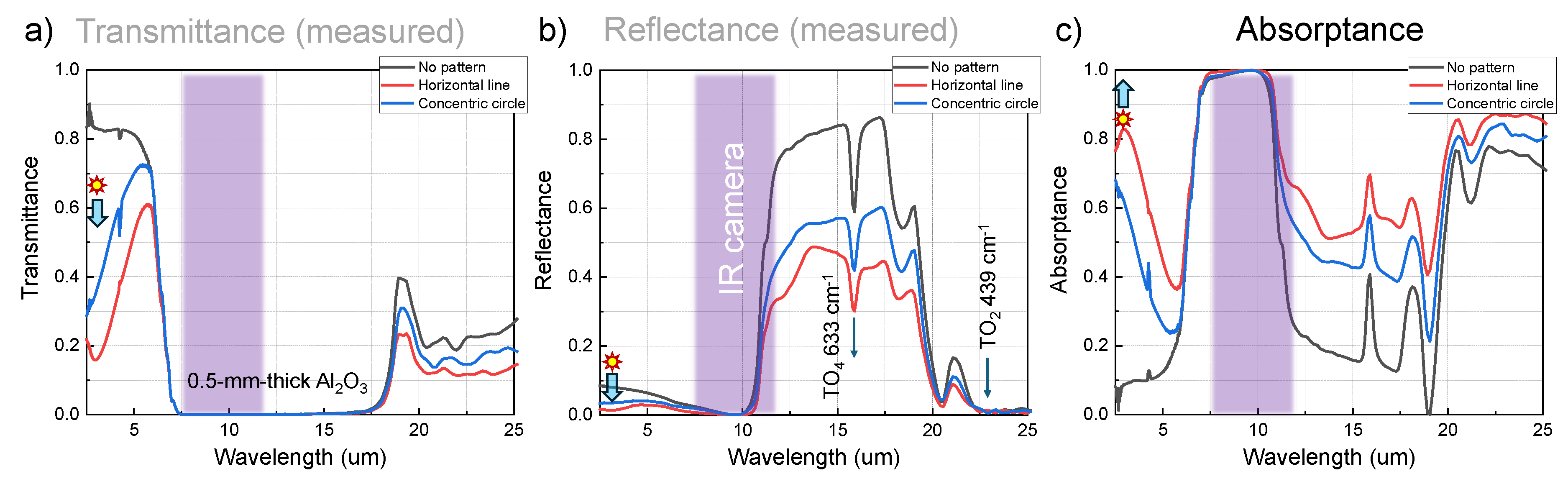
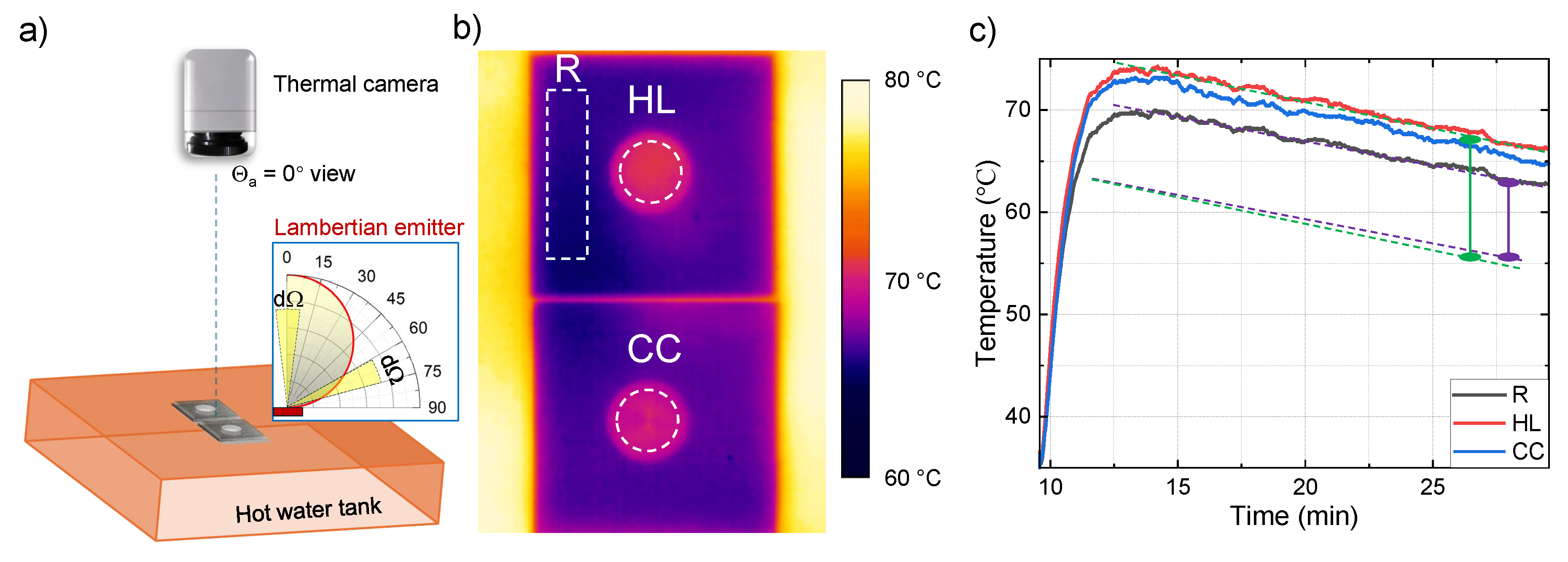
Figure 6.
(a) Temperature measurement setup: sapphire samples were placed in the centre of a hot water tank (polypropylene), with a thermal camera (Optris PI 160, Germany) positioned above (azimuth ) the sample to capture temperature data. Inset shows an emissivity angular diagram for the Lambertian source , is the solid angle wedge into which the black body source emits (see discussion in the text). (b) Thermal image captured by the camera, showing monitored areas with the horizontal line (HL) and concentric circle (CC) patterns, as well as a non-patterned sapphire surface as a reference (R). (c) Cooling transients: temperature change from the monitored areas.
3.3. Thermal Emission and Angular Dependence
According to the Stefan-Boltzmann law , the total power radiated by a black body P [W] is proportional to the , where W/ is the Stefan-Boltzmann constant defined by the basic constants ( Boltzman’s, h Planck’s, and speed of light c), A [] is the surface area, and T [K] is the temperature of the black body [38].
The observed radiant intensity I [W/srad], i.e., the radiant flux (or irradiance [W/]) per unit of solid angle, from an ideal diffusely emitting (or reflecting) surface is directly proportional to the cosine of the angle between the observer’s line of sight and the surface normal. Hence, for the ideal emitter (reflector) , the number of photons per second (J/s=W) emitted into the wedge at angle is , where is the solid angle to which the emitting area subtends at observer (e.g., detector). Therefore, the emission rate in photons/s in a normal and off-normal direction is proportional to the area of the wedge . However, for a Lambertian emitter, the intensity in photons/(s·sr·) remains the same in both the normal and off-normal directions. This is because the emittance scales with , and the solid angle variation compensates for the intensity change. Since the blackbody radiation is uniform with no directionality, the radiation intensity of a blackbody depends on the radiant emittance as [W/(srad)].
Next, surface emissivity with laser-ablated patterns at different orientations was tested to check if such patterned surfaces exhibit Lambertian-emitter nature or if there is Wolf’s effect with preferred directions of light extraction (Eqn. 3). An IR camera integrating response over 7.5–13 m spectral window was used. Notably, measurements of surface temperature (black body radiation) at different azimuthal tilt from the ideal Lambertian emitter will result in different surface temperature readings due to different photon numbers per time (power) emitted towards the camera. Therefore, the same surface will appear to have different temperature values when measured using a detector based on the micro-bolometry principle, which relies on resistance changes due to absorbed photon flux. This effect was experimentally observed and is discussed as follows.
The temperature of HL and CC patterned areas were measured and compared with a non-patterned area as the reference (R) summarised in Figure 6. For each monitored area, the area average temperature is defined as , where N is the total number of pixels, and is the temperature of the i pixel. The thermal camera measures the intensity of IR radiation emitted from the surface and then determines the temperature by quantifying the amount of infrared emission it received in the spectral window 7.5–13 m. According to Planck’s and Stefan-Boltzmann’s law [38], the higher temperature corresponds to higher IR emission from the sample. Thus, by measuring the temperature at different points on the sample’s surface, the thermal camera provides information about the thermal emissivity. This relationship between temperature and emitted power enables the estimation of the sample’s emissivity properties, as materials with higher emissivity will emit more IR radiation at a given temperature compared to those with lower emissivity. Figure 6(c) shows that laser-ablated gratings showed approximately (3-6)% larger temperature, demonstrating the grating pattern has a larger emissivity than a non-patterned area. There was also a slightly faster cooling (see dotted lines). However, the effect was within the uncertainty range.
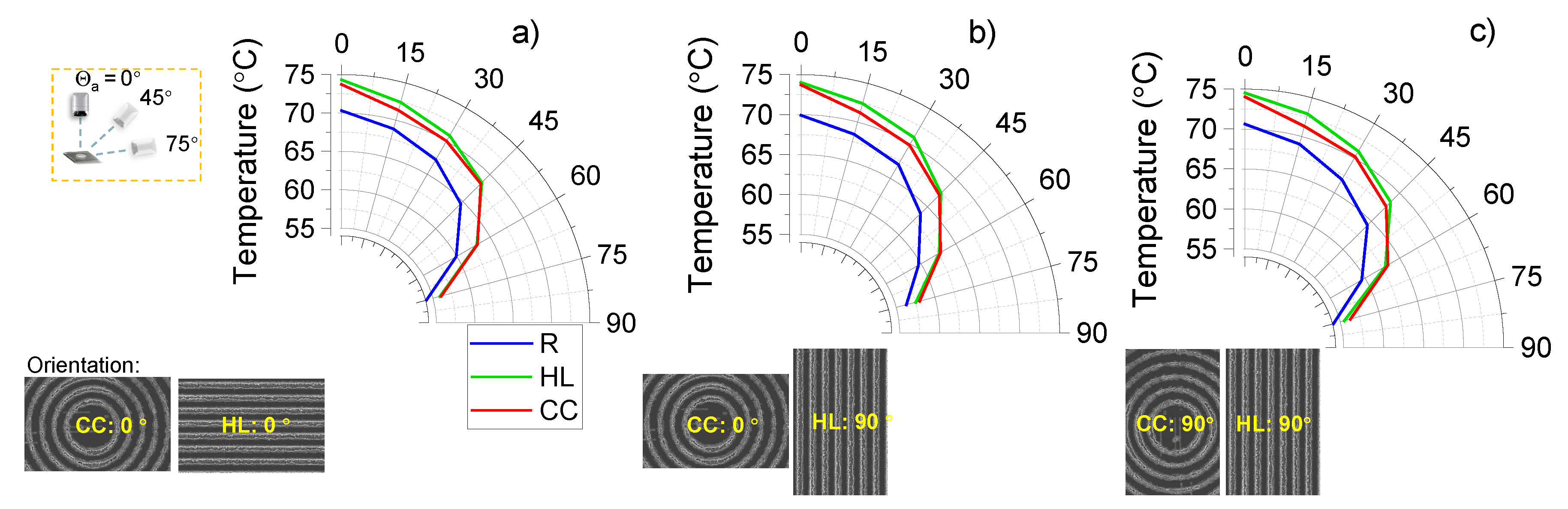
The surface temperature was also measured with the same experimental setup at different azimuthal angles (Figure 7). The angular measurements were taken at an increment of , starting from (top view) and reaching up to . The measurement started when the sample temperature stabilised at . The angular thermal emission was determined for different orientations of the linear and circular grating samples. A close to the Lambertial angular profile for emitted intensity was observed in the temperature determined from the sample’s radiation (Figure 7). Geometrical anisotropy in patterns can influence the IR absorption due to orientation-sensitive scattering effects [39], which is also shown in the angular emission result. As discussed in Section 3.2, deeper grooves and more pronounsed ripples formed when laser polarisation was perpendicular to the scanning direction (Figure 4 (B1)) compared to when it was parallel to the scanning direction (Figure 4 (B2)). As a result, the CC patterned area shows a higher angular emission at large azimuthal angles (), which is most obvious in Figure 7 (c). At small azimuthal angles (), the HL pattern is more dominant in IR emission. The orientation-dependence is also shown by comparing the temperature difference of HL and CC patterns at small azimuthal angles, though the effect is not very pronounced. These optical anisotropy features were also studied in natural spider silk [40] and artificial nanomaterials [41,42].
4. Conclusions and Outlook
Fs-laser ablation on sapphire was investigated for structure formation at different pulse fluence and the number of passes . Spectral and thermal emission characteristics were analysed on 0.5 mm thick sapphire chips with m circular and linear gratings. The overall emissivity was significantly enhanced for both grating types. Such improvement also appears at 7-13 m atmospheric transmission window, which is crucial for radiative cooling applications. The Lambertian nature of surface emitters was confirmed by measuring thermal emission (photons flux) at different azimuthal angles using an IR camera. Fs-laser ablated gratings increased emissivity by (3-6)% compared to the bare sapphire surface.
Direct measurements of emissivity on laser-machined sapphire using both laboratory-based and synchrotron-based FTIR techniques were required to test long wavelengths in IR emissions and Reststrahlen bands, where Wolf’s effect and direction out-coupling of IR light were expected.
Author Contributions
Conceptualization, N.Z., Y.N., S.J.; methodology, N.Z.,S.H.N., H.-H.H. and T.K.; validation, N.Z., D.S., D.S., L.G., D.A., J.V.; formal analysis, N.Z. N.H.A.L.; investigation, N.Z., H.M.; data curation, N.Z., Y.N.; writing—original draft preparation, N.Z., S.J., H.-H.H.; writing—review and editing, all the authors; visualization, N.Z. and S.J.; supervision, S,J. All authors have read and agreed to the published version of the manuscript.
Funding
This research was partly funded by the Australian Research Council Linkage LP220100153 and Discovery DP240103231 grants.
Data Availability Statement
All the data are presented within this manuscript.
Acknowledgments
We acknowledge support by Swinburne University of Technology for the operation of Nanolab. We are grateful to Prof. Jeremy Brown for radiation safety discussions. We thank Workshop-of-Photonics (WOP) Ltd., Lithuania for the patent license and technology transfer project by which the industrial fs-laser fabrication setup was acquired for Nanolab, Swinburne. Synchrotron-FTIR experiments were conducted on the IRM beamline at the Australian Synchrotron, part of ANSTO, through merit-based beamtime proposals (ID. M22505 and M20039) using Al2O3 as a reference.
Conflicts of Interest
The authors declare no conflicts of interest.
Appendix A. Four Polarisation R(λ) from Linear and Circular Al2O3 Gratings
Figure A1.
Reflectance FTIR spectra from c-plane Al2O3 without laser patterned gratings as well as from 0.5-mm-diameter m period linear and circular gratings in (a,b,c), respectively, at different polarisation angles ; inset in (a) shows the geometry of measurements. The top-inset in (b) shows the angular dependence of R vs. angle of linearly polarised incident IR radiation from a thermal IR source (Globar™) at m. Numerical aperture of Cassegranian objective lens , which defined focal diameter m at m, i.e., . Note: R spectra are shown only up to a wavelength of 17.5 m, as the mesh polariser introduces significant noise beyond this range, making the spectrum unreliable due to its inherent design limitations.
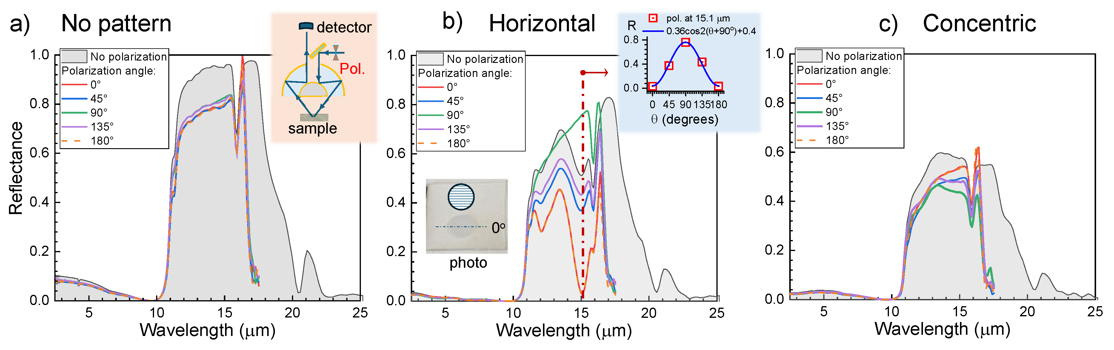
Four-polarisation (4-pol.) method with linearly polarised incidence at four angles with separation allows to define the orientation of the sample where the strongest absorption occurs from a fit , where amplitude and offset of the fit are , respectively [43,44]. The 4-pol. method is applicable for far-field as well as near-field (non-propagating) [43,44]. Figure A1 has a summary of results, which reveal that reflectance R was orientationally isotropic for bare c-plance Al2O3 and circular grating pattern milled by laser ablation (a) and (c). Very strong modulation for linear grating was observed at m (inset on Figure A1(b)).
References
- Hu, J.; Xu, K.; Huang, P.; Wang, M.; Xu, S.; Wei, Q.H. Hierarchical Conical Metasurfaces as Ultra-Broadband Perfect Absorbers from Visible to Far-Infrared Regime. 34, 2309229. _eprint. [CrossRef]
- Reicks, A.; Tsubaki, A.; Anderson, M.; Wieseler, J.; Khorashad, L.K.; Shield, J.E.; Gogos, G.; Alexander, D.; Argyropoulos, C.; Zuhlke, C. Near-unity broadband omnidirectional emissivity via femtosecond laser surface processing. 2, 1–11. Publisher: Nature Publishing Group. [CrossRef]
- Nishijima, Y.; Kimura, S.; Takeshima, Y.; Juodkazis, S. Metasurfaces as Energy Valves for Sustainable Energy Management. 13, 1769. Number: 10 Publisher: Multidisciplinary Digital Publishing Institute. [CrossRef]
- Bonse, J.; Kirner, S.V.; Griepentrog, M.; Spaltmann, D.; Krüger, J. Femtosecond Laser Texturing of Surfaces for Tribological Applications. 11, 801. Number: 5 Publisher: Multidisciplinary Digital Publishing Institute. [CrossRef]
- Mao, B.; Siddaiah, A.; Liao, Y.; Menezes, P.L. Laser surface texturing and related techniques for enhancing tribological performance of engineering materials: A review. 53, 153–173. [CrossRef]
- Ijaola, A.O.; Bamidele, E.A.; Akisin, C.J.; Bello, I.T.; Oyatobo, A.T.; Abdulkareem, A.; Farayibi, P.K.; Asmatulu, E. Wettability Transition for Laser Textured Surfaces: A Comprehensive Review. 21, 100802. [CrossRef]
- Yang, C.j.; Mei, X.s.; Tian, Y.l.; Zhang, D.w.; Li, Y.; Liu, X.p. Modification of wettability property of titanium by laser texturing. 87, 1663–1670. [CrossRef]
- Jalil, S.A.; Lai, B.; ElKabbash, M.; Zhang, J.; Garcell, E.M.; Singh, S.; Guo, C. Spectral absorption control of femtosecond laser-treated metals and application in solar-thermal devices. 9, 14. Publisher: Nature Publishing Group. [CrossRef]
- Zheng, N.; Buividas, R.; Huang, H.H.; Stonytė, D.; Palanisamy, S.; Katkus, T.; Kretkowski, M.; Stoddart, P.R.; Juodkazis, S. Laser Machining at High PW/cm2 Intensity and High Throughput. 11, 598. Number: 7 Publisher: Multidisciplinary Digital Publishing Institute. [CrossRef]
- Juodkazis, S.; Buividas, R.; Huang, H.H.; Stonytė, D.; Palanisamy, S.; Zhu, D.M.; Katkus, T.; Kretkowski, M.; Nishijima, Y.; Grineviciute, L.; et al. Femtosecond Laser Textured Surfaces for Radiative Cooling: Black Metals. [CrossRef]
- Efimov, O.; Juodkazis, S.; Misawa, H. Intrinsic single- and multiple-pulse laser-induced damage in silicate glasses in the femtosecond-to-nanosecond region. Physical Review A 2004, 69, 042903, Publisher: American Physical Society. [Google Scholar] [CrossRef]
- Vanagas, E.; Kudryashov, I.; Tuzhilin, D.; Juodkazis, S.; Matsuo, S.; Misawa, H. Surface nanostructuring of borosilicate glass by femtosecond nJ energy pulses. Applied Physics Letters 2003, 82, 2901–2903. [Google Scholar] [CrossRef]
- Juodkazis, S.; Rode, A.; Gamaly, E.; Matsuo, S.; Misawa, H. Recording and reading of three-dimensional optical memory in glasses. Applied Physics B 2003, 77, 361–368. [Google Scholar] [CrossRef]
- Zhang, Y.; Jiang, Q.; Long, M.; Han, R.; Cao, K.; Zhang, S.; Feng, D.; Jia, T.; Sun, Z.; Qiu, J.; et al. Femtosecond laser-induced periodic structures: mechanisms, techniques, and applications. Opto-Electronic Science 2022, 1, 220005. [Google Scholar] [CrossRef]
- Dharmavarapu, R.; Izumi, K.i.; Katayama, I.; Ng, S.H.; Vongsvivut, J.; Tobin, M.J.; Kuchmizhak, A.; Nishijima, Y.; Bhattacharya, S.; Juodkazis, S. Dielectric cross-shaped-resonator-based metasurface for vortex beam generation at mid-IR and THz wavelengths. Nanophotonics 2019, 8, 1263–1270, Publisher: De Gruyter. [Google Scholar] [CrossRef]
- Baranov, D.G.; Xiao, Y.; Nechepurenko, I.A.; Krasnok, A.; Alù, A.; Kats, M.A. Nanophotonic engineering of far-field thermal emitters. 18, 920–930. Publisher: Nature Publishing Group. [CrossRef]
- Sergeeva, K.A.; Pavlov, D.V.; Seredin, A.A.; Mitsai, E.V.; Sergeev, A.A.; Modin, E.B.; Sokolova, A.V.; Lau, T.C.; Baryshnikova, K.V.; Petrov, M.I.; et al. Laser-Printed Plasmonic Metasurface Supporting Bound States in the Continuum Enhances and Shapes Infrared Spontaneous Emission of Coupled HgTe Quantum Dots. 33, 2307660. [CrossRef]
- Engelbrecht, J.A.A.; van Rooyen, I.J.; Henry, A.; Janzén, E.; Olivier, E.J. The origin of a peak in the reststrahlen region of SiC. Physica B: Condensed Matter 2012, 407, 1525–1528. [Google Scholar] [CrossRef]
- Schubert, M.; Tiwald, T.E.; Herzinger, C.M. Infrared dielectric anisotropy and phonon modes of sapphire. Physical Review B 2000, 61, 8187–8201, Publisher: American Physical Society. [Google Scholar] [CrossRef]
- Streyer, W.H. Reststrahlen band optics for the advancement of far-infrared optical architecture. PhD thesis, University of Illinois at Urbana-Champaign, 2016.
- Lee, S.C.; Ng, S.S.; Abu Hassan, H.; Hassan, Z.; Dumelow, T. Crystal orientation dependence of polarized infrared reflectance response of hexagonal sapphire crystal. Optical Materials 2014, 37, 773–779. [Google Scholar] [CrossRef]
- Greffet, J.J.; Carminati, R.; Joulain, K.; Mulet, J.P.; Mainguy, S.; Chen, Y. Coherent emission of light by thermal sources. Nature 2002, 416, 61–64, Publisher: Nature Publishing Group. [Google Scholar] [CrossRef]
- Wolf, E. Non-cosmological redshifts of spectral lines. Nature 1987, 326, 363–365, Publisher: Nature Publishing Group. [Google Scholar] [CrossRef]
- Wolf, E.; James, D.F.V. Correlation-induced spectral changes. Reports on Progress in Physics 1996, 59, 771. [Google Scholar] [CrossRef]
- Wang, X.W.; Seniutinas, G.; Balcytis, A.; Kasalynas, I.; Jakstas, V.; Janonis, V.; Venckevicius, R.; Buividas, R.; Appadoo, D.; Valusis, G.; et al. Laser structuring for control of coupling between THz light and phonon modes, 2016. arXiv:1605.04493 [cond-mat]. [CrossRef]
- Takayama, N.; Asaka, S.; Yan, J. Nanosecond pulsed laser irradiation of sapphire for developing microstructures with deep V-shaped grooves. 52, 440–450. [CrossRef]
- Chang, C.W.; Chen, C.Y.; Chang, T.L.; Ting, C.J.; Wang, C.P.; Chou, C.P. Sapphire surface patterning using femtosecond laser micromachining. 109, 441–448. [CrossRef]
- Stern, L.; Grajower, M.; Levy, U. Fano resonances and all-optical switching in a resonantly coupled plasmonic–atomic system. Nature Communications 2014, 5, 4865, Publisher: Nature Publishing Group. [Google Scholar] [CrossRef] [PubMed]
- Rybin, M.V.; Samusev, K.B.; Sinev, I.S.; Semouchkin, G.; Semouchkina, E.; Kivshar, Y.S.; Limonov, M.F. Mie scattering as a cascade of Fano resonances. Optics Express 2013, 21, 30107–30113, Publisher: Optica Publishing Group. [Google Scholar] [CrossRef] [PubMed]
- Grineviciute, L.; Lukosiunas, I.; Nikitina, J.; Selskis, A.; Meskelaite, I.; Gailevicius, D.; Staliunas, K. Light Trapping by Non-Hermitian Thin Films, 2024. arXiv:2410.15101 [physics]. [CrossRef]
- Grineviciute, L.; Nikitina, J.; Babayigit, C.; Staliunas, K. Fano-like resonances in nanostructured thin films for spatial filtering. Applied Physics Letters 2021, 118, 131114. [Google Scholar] [CrossRef]
- Liu, X.Q.; Zhang, Y.L.; Li, Q.K.; Zheng, J.X.; Lu, Y.M.; Juodkazis, S.; Chen, Q.D.; Sun, H.B. Biomimetic sapphire windows enabled by inside-out femtosecond laser deep-scribing. PhotoniX 2022, 3, 1. [Google Scholar] [CrossRef]
- Wang, H.; Zhang, F.; Wang, C.; Duan, J. Broadband antireflective subwavelength structures for infrared detection. Optics & Laser Technology 2022, 149, 107931. [Google Scholar] [CrossRef]
- Honsberg, C.; Bowden, S. Absorption Coefficient, 2019.
- Gamaly, E.G.; Rode, A.V.; Luther-Davies, B.; Tikhonchuk, V.T. Ablation of solids by femtosecond lasers: Ablation mechanism and ablation thresholds for metals and dielectrics. Physics of Plasmas 2002, 9, 949–957. [Google Scholar] [CrossRef]
- Zhang, L.; Mu, K.; Zhou, Y.; Wang, H.; Zhang, C.; Zhang, X.C. High-power THz to IR emission by femtosecond laser irradiation of random 2D metallic nanostructures. 5, 12536. Publisher: Nature Publishing Group. [CrossRef]
- Palanza, V.; Di Martino, D.; Paleari, A.; Spinolo, G.; Prosperi, L. Micro-Raman spectroscopy applied to the study of inclusions within sapphire. Journal of Raman Spectroscopy 2008, 39, 1007–1011. [Google Scholar] [CrossRef]
- Planck, M. The Theory of Heat Radiation; Blakiston, 1914; pp. 1–3, 14–16, 40–42.
- Dao, T.D.; Ishii, S.; Doan, A.T.; Wada, Y.; Ohi, A.; Nabatame, T.; Nagao, T. An On-Chip Quad-Wavelength Pyroelectric Sensor for Spectroscopic Infrared Sensing. 6, 1900579. _eprint: https://onlinelibrary.wiley.com/doi/pdf/10.1002/advs.201900579. [CrossRef]
- Linklater, D.; Vailionis, A.; Ryu, M.; Kamegaki, S.; Morikawa, J.; Mu, H.; Smith, D.; Maasoumi, P.; Ford, R.; Katkus, T.; et al. Structure and Optical Anisotropy of Spider Scales and Silk: The Use of Chromaticity and Azimuth Colors to Optically Characterize Complex Biological Structures. 13, 1894. Number: 12 Publisher: Multidisciplinary Digital Publishing Institute. [CrossRef]
- Li, Z.; Yin, Y. Stimuli-Responsive Optical Nanomaterials. 31, 1807061. _eprint. [CrossRef]
- Zonov, R.; Fateev, A.; Obraztsov, A.; Mikheev, G. Wavelength-Dependent Photocurrent Generation Efficiency in the Carbon Nanowall Films. 260, 2200540. _eprint. [CrossRef]
- Hikima, Y.; Morikawa, J.; Hashimoto, T. FT-IR Image Processing Algorithms for In-Plane Orientation Function and Azimuth Angle of Uniaxially Drawn Polyethylene Composite Film. Macromolecules 2011, 44, 3950–3957, Publisher: American Chemical Society. [Google Scholar] [CrossRef]
- Meguya, R.; Hock Ng, S.; Han, M.; Anand, V.; Katkus, T.; Vongsvivut, J.; Appadoo, D.; Nishijima, Y.; Juodkazis, S.; Morikawa, J. Polariscopy with optical near-fields. Nanoscale Horizons 2022, 7, 1047–1053, Publisher: Royal Society of Chemistry. [Google Scholar] [CrossRef]
Figure 1.
Front-side ablation of Al2O3. (a) Transmittance T (wavenumber is in log-scale) and (b) reflectance R measured in mid-to-far IR spectral range; insets show optical images of laser ablated Al2O3; single-point measurements were carried out on the laser-ablated regions (numbers are indicated on insets); laser: central wavelength nm, pulse duration fs, repetition rate kHz, pulse energy J, numerical aperture (focal diameter m); the grating period was 12.5 m with m depth of the ablated-groove; depth defined by ablation fluence, scan speed and number of repeated passes (without change of vertical focal spot position). Constant density of pulses 100 for shallow gratings and 500 for deep gratings was used.
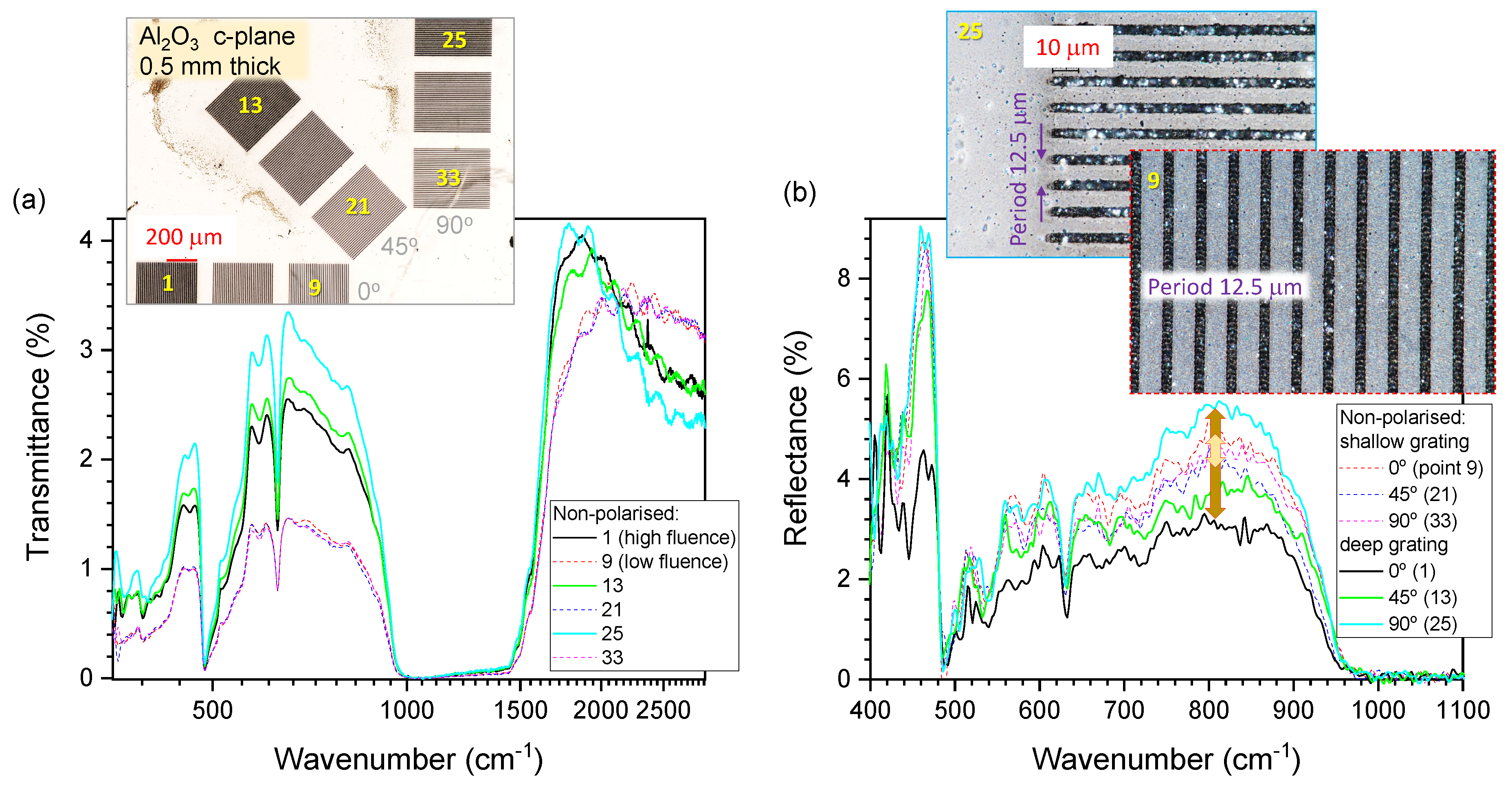
Figure 7.
Lambertian-like emitter surfaces. Measurement of temperature of sapphire samples at the azimuthal observation angles from to angle at and orientations (orientation in the plane of the sample). (a) HL at and CC at orientation. (b) HL at and CC at orientation. (c) HL at and CC at orientation. The setup is the same as Figure 6 to record the temperature at different angles like the insert shown in (a).
Disclaimer/Publisher’s Note: The statements, opinions and data contained in all publications are solely those of the individual author(s) and contributor(s) and not of MDPI and/or the editor(s). MDPI and/or the editor(s) disclaim responsibility for any injury to people or property resulting from any ideas, methods, instructions or products referred to in the content. |
© 2025 by the authors. Licensee MDPI, Basel, Switzerland. This article is an open access article distributed under the terms and conditions of the Creative Commons Attribution (CC BY) license (http://creativecommons.org/licenses/by/4.0/).
Copyright: This open access article is published under a Creative Commons CC BY 4.0 license, which permit the free download, distribution, and reuse, provided that the author and preprint are cited in any reuse.


