Preprint
Communication

Preparation of Air Stable Lead-Free CsSnI3 Perovskites: Synthesis Based on CsI and SnCl2 Solutions

Altmetrics

Downloads

32

Views

18

Comments

0

A peer-reviewed article of this preprint also exists.

Submitted:

29 November 2024

Posted:

29 November 2024

You are already at the latest version

Alerts
Abstract

Objective: This study focuses on the synthesis and analysis of the morphology of CsSnI3 crystals and films based on CsI and SnCl2 solutions. The aim of this approach is to synthesize air-stable perovskites and prevent phase transitions of tin-containing perovskite, where previous studies have often reported its rapid oxidation when dissolved in dimethyl sulfoxide. Methods: CsSnI3 crystalline films were obtained from CsI and SnCl2 solutions, in which deionized water and ultrapure ethanol were used for their dissolution. Dissolution and mixing were performed at room temperature. High-purity CsI (99.99%) and SnCl2 (99.99%) powders were used to obtain solutions. To obtain a homogeneous CsSnl3 solution, the SnCl2 solution was added dropwise to the CsI solution and stirred on a magnetic stirrer at 900 rpm. The resulting solution was then applied to FTO substrates heated on a hotplate without spin coating. The samples were heated to temperatures from 60 0C to 130 0C, where, depending on the rate of evaporation of the liquid, the process of formation of crystalline and thin-film structures was controlled. Results: Stable CsSnI3 films were obtained. SEM and X-ray diffraction analyses of the obtained cesium tin triiodide films deposited on conventional FTO glass substrates were performed. X-ray diffraction patterns of synthesized perovskite crystals and films were obtained. Conclusion: The synthesized CsSnI3 perovskite thin films retained their black perovskite phase for more than 4 months, indicating their long-term stability. Based on the results and long-term stability performance, it can be concluded that the black phases of CsSnI3 are suitable for various applications such as photovoltaic devices.

Keywords: 
Subject: Chemistry and Materials Science  -   Surfaces, Coatings and Films

1. Introduction

In recent years, solar photovoltaic technology has been developing rapidly, and to advance in this field, it is always necessary to develop high-efficiency devices based on affordable and cost-effective materials [1]. Including CdTe, CiGS, amorphous Si, monocrystalline Si, GaAs, organic photovoltaic cells, graphene solar cells and other functional materials have found wide applications in the field of photovoltaics, but each particular material is characterized by its own disadvantages, including toxicity, shortcomings of the original sire, disadvantages technological process of panel fabrication, etc. [2]. As is known, the 21st century has acquired the name of the century of silicon, but all such despite the laudable characteristics of this material there are some shortcomings. For example, silicon-based solar cells have been found to have a number of drawbacks including cost, correlation of efficiency with weather conditions, space requirements, pollution problems, rigidity and high manufacturing costs [3]. In addition, pure silicon-based materials have long since reached the theoretical limit of Schottky efficiency [4]. Therefore, in current technologies, new types of photovoltaic devices are associated with sensitized solar cells such as quantum dots and perovskite solar cells. Among them, perovskite solar cells have the advantage of low manufacturing cost and structurally regulated materials. Recently, perovskite solar cells, called “third generation solar cells”, have emerged and have been widely promoted as economically and environmentally viable and renewable technologies compared to conventional solar cell technologies to solve global energy, safety and environmental problems [5]. Moreover, the latest perovskite solar cells can convert energy with up to 26.7% efficiency [6]. Recently, a theoretical achievement of over 46% efficiency of solar inverters based on perovskite materials by focusing with a light lens in a small photovoltaic cell has been reported [3]. Among materials with perovskite structure (ABX3, where A is an organic or inorganic cation that coordinates with 12X anions, B is a divalent metal that coordinates with 6X anions, and X is a halide ion [7]), FAPbI3, MAPbI3, CsPbI3, and other lead-containing perovskites have shown good efficiency as it is committed in recent studies. However, the presence of toxic lead makes us think about replacing the B position with another element that does not strongly affect on the perovskites bandgap. The conversion efficiency of solar cells depends on the optical properties of materials, the so-called ability to absorb light, which, in turn, strongly depends on the bandgap width of the materials. It is known that halide perovskites of the CsSnX3 family can be a suitable candidate to maximize the absorption ability. However, the presence of tin in the perovskite matrix makes them thermally unstable at temperatures closer to normal conditions. The most stable perovskites with tin content, such as CsSnCl3 and CsSnF3 have large band gaps, so the actual task is to develop new methods of synthesis and stabilization of CsSnI3, CsSnBr3 or Sn-containing stable perovskites with shifted halogen compositions with optimal bandgap.
In this work, we report the preparation of stable crystals and thin films with perovskite structure by solution reaction of CsI (99.99 %) and SnCl2 (99.99 %) containing salts.

2. Experimental Methodology

To obtain clean surfaces, the substrates were cleaned in 4 steps using an ultrasonic bath. Washed glass substrates of 2.5x2.5 cm were used for perovskite coating. The first washing step is carried out for 10 minutes using distilled water (with the addition of liquid soap). The process is then repeated with distilled water without soap (10 minutes). The substrates are then washed in ultrapure acetone (99.99%) and isopropanol (99.99%), each of which also takes 10 minutes. After evaporation of the residual isopropanol, the substrates are cleaned by UV light in a UV-OZONE cleaning device for 30 minutes. After sufficient cleaning of the substrate, the preparation of thin film coating solutions was proceeded. A method for forming a CsSnI3 film on a substrate, comprising the following steps:
(a) providing a substrate → (b) providing a homogeneous solution of CsSnI3 → (c) depositing droplets of the homogeneous CsSnI3 solution on the substrate → (d) heating the substrate after step (c) to remove the solvent in the homogeneous CsSnI3 solution until the substrate is dry → (e) forming a CsSnI3 film on the substrate.
The method of claim 1, wherein steps (a)-(c) are performed under ambient conditions; steps (d) and (e) is performed at a temperature in the range of from about 50° C to about 90° C in a heating plate.
In the first step, a CsI solution is prepared, which is a CsI solution with a concentration from about 40% by weight obtained by completely dissolving CsI powder in deionized water (Figure 1). A SnCl2 solution containing from about 30% by weight of SnCl2 solution is then prepared by completely dissolving SnCl2 powder in ethyl alcohol (Figure 1). During the reaction, HCl is released from the solution as a gas. We then prepared a homogeneous CsSnl3 solution by adding the SnCl2 solution dropwise to the CsI solution. The CsSnI3 solution was then stirred in a magnetic stirrer at a speed of 900 revolutions/min to obtain the homogeneous CsSnI3 solution. During the mixing process, the color of the clear SnCl2 and CsI solutions first turns black and then yellow. Then, the obtained yellow solution was deposited directly on glass substrates heated in a hot plate without performing spin-coating procedure.

3. Results and Discussion

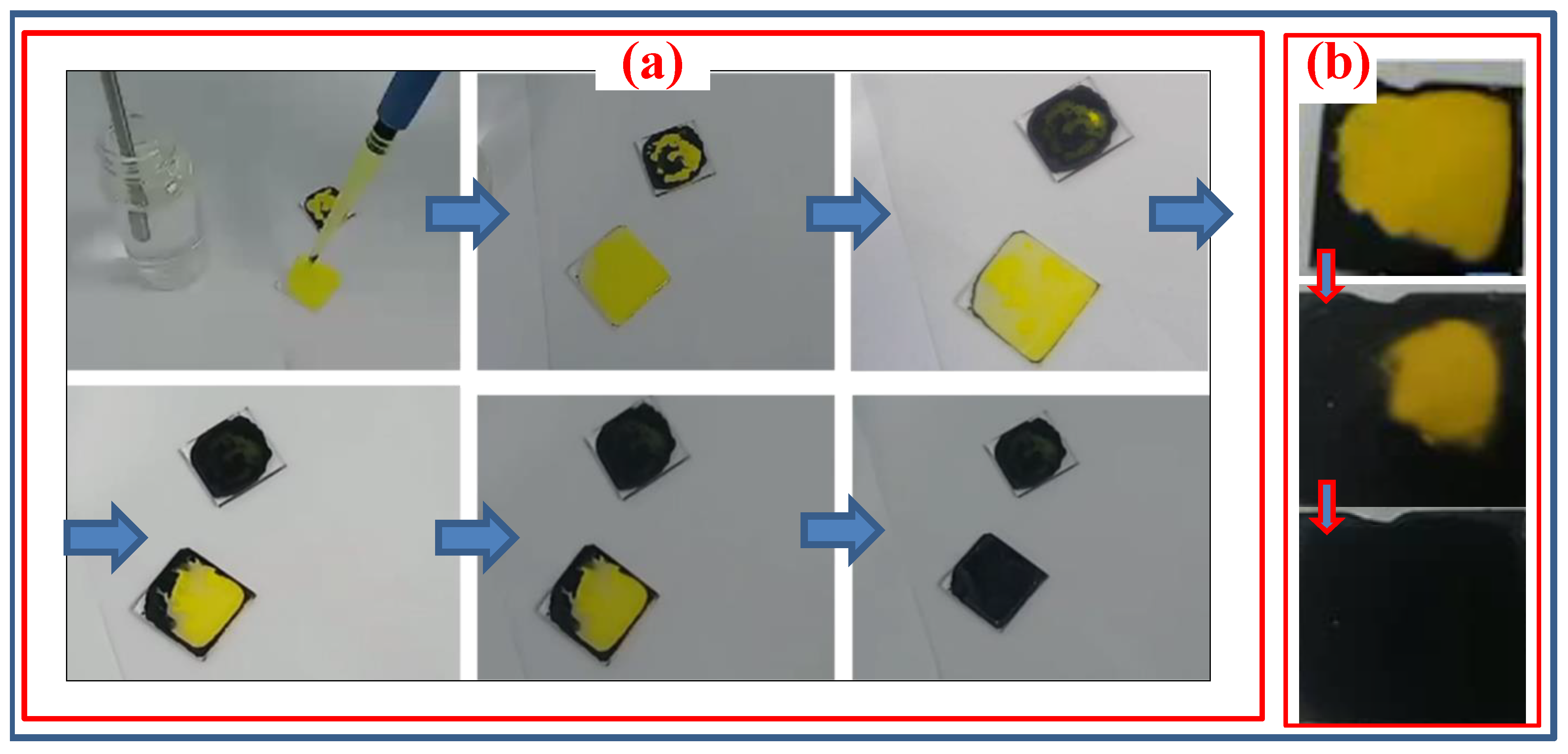
After obtaining a homogeneous solution, the films were deposited on glass substrates directly on the heating plate without the spin coating procedure. Figure 2 shows snapshots of the sintering process of CsSnl3 films and their color change upon heating at a constant temperature of 600C.
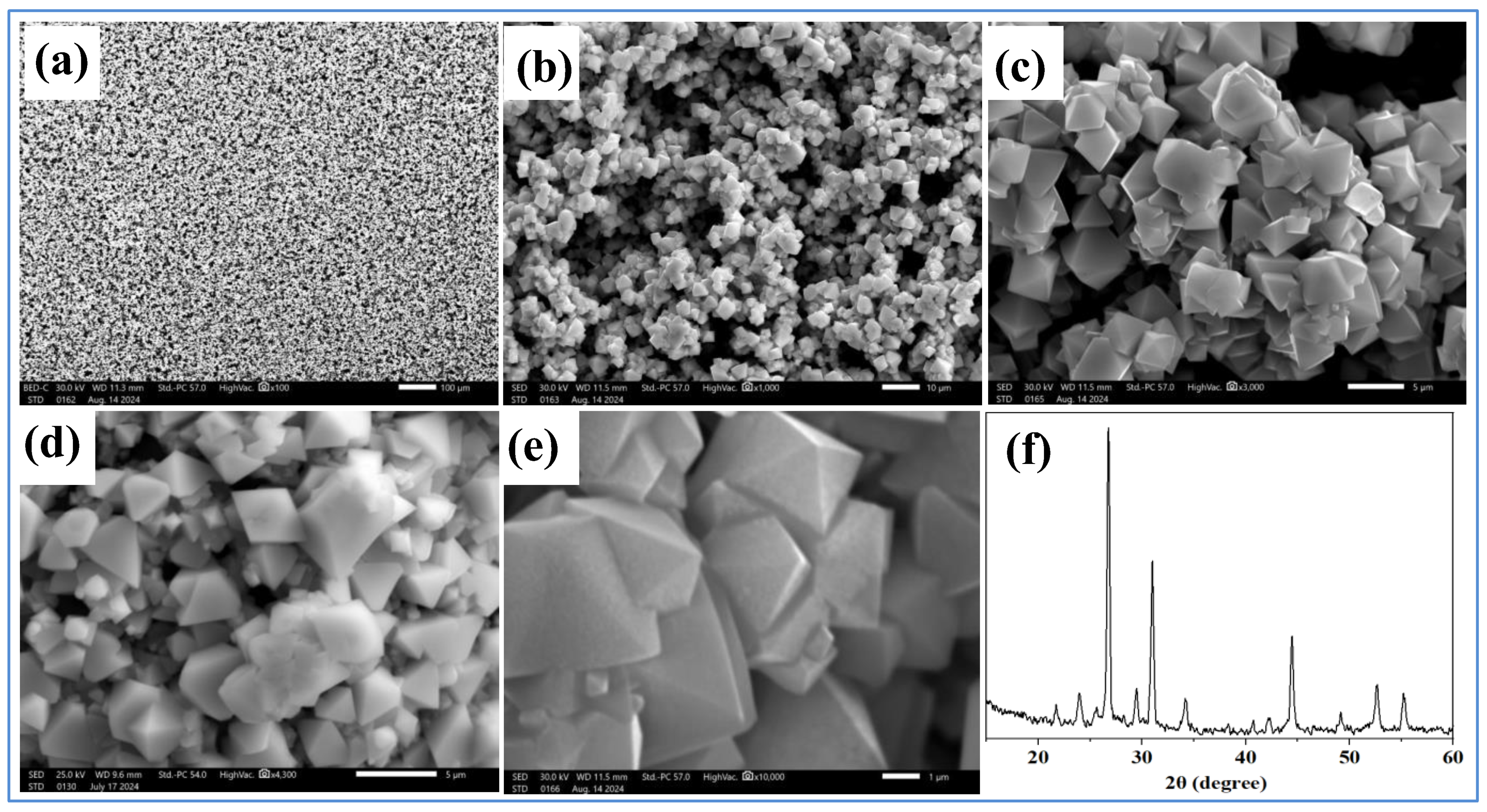
It can be seen that after heating, a black film with a mesoporous morphology with an ordered internal structure and rhombic crystallites is formed on the surface of the glass substrate (Figure 3 (a-e)). The results of XRD analysis of the obtained samples using a Dron 2 diffractometer are shown in Figure 3 (e).
However, when the temperature was increased to 1300 C, a radical change was noted (Figure 2 (b)): the resulting crystals became more agglomerated, forming a thin-film structure, the results of SEM analysis of which are shown in Figure 4 (a, b) at magnifications of 3500 and 7500 times. Despite the fact that in all previous works the authors report about instability of this perovskite structure, the samples obtained by us retain the black phase of perovskite for more than 4 months and only some samples partially change color to yellow. However, for many samples obtained using this methodology, no changes have yet been detected.
It should be noted that since we did not have an XRD machine, X-ray structural analysis of the obtained samples was carried out only after 2 days.

Conclusions

We successfully synthesized crystalline thin films of perovskite CsSnI3 by a simple method of mixing CsI and SnCl2 solutions. According to the results, it can be seen that this technique can be used to obtain very stable structures of CsSnI3, however, it is necessary to repeated experiments with different ratios of salts and solvents, with step-by-step temperature adjustments to optimize the morphology and thickness of the initial thin film.

Author Contribution

Methodology: Dilshod Nematov and Amondulloi Burkhonzoda; Software: Amondulloi Burkhonzoda; Validation: Kholmirzo Kholmurodov; Formal analysis: Ashurov Anushervon; Investigation, Dilshod Nematov and Dilshod Nematov and Amondulloi Burkhonzoda; Resources: Dilshod Nematov; Data curation: Amondulloi Burkhonzoda; Writing—review & editing: Dilshod Nematov and Kholmirzo Kholmurodov; Supervision: Dilshod Nematov; Project administration: Dilshod Nematov; Funding acquisition: Dilshod Nematov. All authors have read and agreed to the published version of the manuscript.

Funding Acknowledgements

The work was performed at the S.U. Umarov Physical-Technical Institute of the National Academy of Sciences of Tajikistan with the support of International Science and Technology Center (ISTC), project TJ-2726. The author expresses his deep gratitude to the Government of Japan for financial support of this project and the establishment of a modern laboratory at the PhTI, NAST.

Conflicts of Interest

The author declared no conflict of interest.

Abbreviation List

DMF, Dimethyl formamide
DMSO, Dimethyl sulfoxide
CsI, Cesium Iodide
SnCl2, Tin(II) chloride
XRD, X-ray diffraction
SEM, Scanning electron microscope
FTO, Fluorine-doped Tin Oxide
UV, Ultraviolet

References

  1. Dada M, Popoola P. Recent advances in solar photovoltaic materials and systems for energy storage applications: a review. Beni-Suef University Journal of Basic and Applied Sciences 2023, 12, 1–15. [Google Scholar] [CrossRef]
  2. Polman A, Knight M, Garnett EC at al. Photovoltaic materials: Present efficiencies and future challenges. Science, 2016; 352. [CrossRef]
  3. Shah, A. Amorphous silicon solar cells. Solar Cells and Modules 2020, 4, 139–161. [Google Scholar] [CrossRef]
  4. Jin Y, Seok J, & Yu K. Highly efficient silicon-based thin-film Schottky barrier photodetectors. ACS Photonics 2023, 10, 1302–1309. [Google Scholar] [CrossRef]
  5. Yan J, Saunders BR. Third-generation solar cells: a review and comparison of polymer: fullerene, hybrid polymer and perovskite solar cells. Rsc Advances 2014, 4, 43286–43314. [Google Scholar] [CrossRef]
  6. https://www.nrel.gov/pv/cell-efficiency.html.
  7. Luo J, Im J, Mayer MT, Nazeeruddin MK, at al. Water photolysis at 12.3% efficiencyvia perovskite photovoltaics and earth-abundant catalysts. Science 2014, 345, 1593. [Google Scholar] [CrossRef] [PubMed]
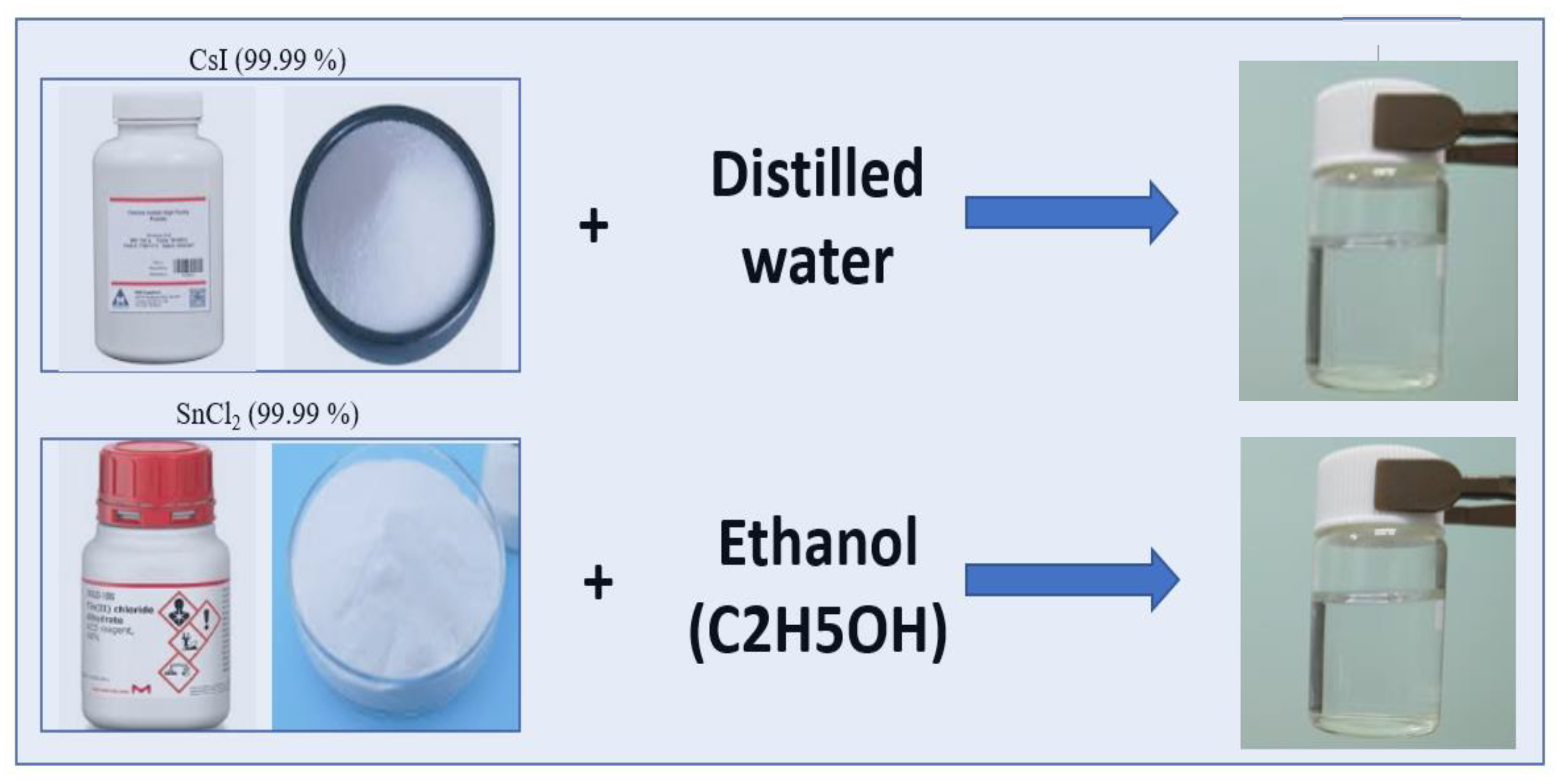
Figure 1. Scheme of preparation of CsI and SnCl2 solutions.
Preprints 141301 g001
Figure 2. Snapshots of the process of formation of perovskite crystalline films at 60 0C (a) and thin films at the 130 0C (b). .
Preprints 141301 g002
Figure 3. SEM images of the obtained samples after 100 (a), 1000 (b), 3000 (c), 5000 (d) and 11000 times magnification.
Preprints 141301 g003
Figure 4. SEM images of crystalline perovskite films (a, b) and their X-ray diffraction patterns (c).
Preprints 141301 g004
Disclaimer/Publisher’s Note: The statements, opinions and data contained in all publications are solely those of the individual author(s) and contributor(s) and not of MDPI and/or the editor(s). MDPI and/or the editor(s) disclaim responsibility for any injury to people or property resulting from any ideas, methods, instructions or products referred to in the content.
Copyright: This open access article is published under a Creative Commons CC BY 4.0 license, which permit the free download, distribution, and reuse, provided that the author and preprint are cited in any reuse.
Prerpints.org logo

Preprints.org is a free preprint server supported by MDPI in Basel, Switzerland.

Subscribe

© 2024 MDPI (Basel, Switzerland) unless otherwise stated