Submitted:
21 October 2024
Posted:
24 October 2024
You are already at the latest version
Abstract
Drawing inspiration from biological brain's energy-efficient information-processing mechanisms, photonic integrated circuits (PIC) have facilitated the development of ultrafast artificial neural networks. This in turn is envisaged to offer potential solutions to the growing demand for artificial intelligence employing machine learning in various domains, from nonlinear optimization and telecommunication to medical diagnosis. At the meantime, silicon photonics has emerged as a mainstream technology for integrated chip based application. However, challenges still need to be addressed in scaling it further for broader applications due to the requirement of co-integration of electronic circuitry for control and calibration. Leveraging physics in algorithms and nanoscale materials holds promise for achieving low-power, miniaturized chips capable of real-time inference and learning. In this back drop, we present the state of the art in neuromorphic photonic computing, focusing primarily on architecture, weighting mechanisms, photonic neurons, and training while giving an over-all view on recent advancements, challenges, and prospects. We also emphasize and high light the need for revolutionary hardware innovations to scale up neuromorphic systems while enhancing energy efficiency and performance.
Keywords:
Neuromorphic Photonics
; Photonic Integrated Circuits
; Optical Computing
; Silicon Photonics
; On-Chip Machine Learning
; Neuromorphic Computing
; Photonic Neural Networks
; Integrated circuits
1. Introduction
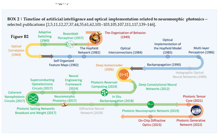
A determined pursuit for computational systems mirroring the efficiency of the human brain has served as a compelling impetus with significant industrial implications right from the emergence of Artificial Intelligence (AI) dating back to 1950s [1,2]. It has undergone an initial surge of optimism followed by decades of setbacks, primarily attributed to the dearth of computing power during that period. Inspired by human brain's neurosynaptic framework [Box 1], AI endeavors to attain the level of precision equivalent to human performance in tasks that pose difficulties for conventional computing systems yet come naturally to humans. The brain's computational power has an efficiency of around aJ/MAC (multiply-accumulate) operation [3]. In contrast, conventional computers generally bound by von Neumann architecture struggled with the architectural scaling typically consumes 100 pJ/MAC operation [3].
In the present era of prolific data generation and escalating automation, AI has emerged as a transformative force [Box 2][4], reshaping industries and redefining human-machine interactions through Machine Learning (ML)[5] and Deep Learning (DL)[6,7]. These developments are influenced by the advent of computing power reflected in the modern Nvidia graphic processing units (GPUs)[8] and Googles's tensor processing units (TPUs)[9] consuming only around 20 PJ/MAC operation sustaining Moore's Law. Some of the current applications of AI extend across various sectors, encompassing autonomous driving, robotic vision, remote sensing, microscopy, surveillance, deterrence, and the Internet of Things[7,10]. The significant accomplishments of AI algorithms, particularly neural networks (NN) [11,12], have influenced numerous facets of our daily lives, ranging from language translation[9] to cancer diagnosis[13].
1.1 Neuromorphic Electronic Computing: On-Chip AI
The technology requirements for AI have evolved[14,15]. NN, the backbone of neuromorphic computing for AI algorithms, consists of artificial neurons arranged in layers connected to others through synapses (Box 1), allowing these networks to adapt and learn from data and exhibiting inherent parallelism and distributed computing features that confront significant hurdles when implemented in digital electronics[16]. This misalignment with the sequential nature of von Neumann architecture with separate central processing units and dynamic random-access memory in digital computers has led to a shift towards on-chip electronics driven by its potential to enhance computational speed and efficiency by co-locating computing and storage units[17,18,19]. State-of-the-art neuromorphic electronic architectures, which rely on transmission lines and active buffering techniques, face challenges in meeting the demands of massive parallel signal fan-out and fan-in[20]. Architectures resort to digital time-multiplexing, enabling the construction of more extensive NNs at the expense of bandwidth that detours the limitations of electronic writing[16].
Industry and research initiatives emphasize the viability of on-chip electronics. Significant achievements in designing application-specific integrated circuits (ASIC) have been observed in noteworthy projects, including IBM's TrueNorth[21], Neurogrid[19], SpiNNaker[17], Tianjic[22], Microsoft Azure Maia AI Accelerator[23], and Intel's Loihi[18]. Co-locating computing units and storage units within the same chip addresses the inefficiencies of traditional architectures[3]. However, challenges persist; interconnect density[24] and bandwidth limitations[16], scalability concerns[20], and power consumption issues[25] underscore the need for continued innovation. The future envisions more sophisticated applications, ranging from nonlinear programming[26] to real-time learning[27] and intelligent signal processing[28], evidenced by recent applications, including The Human Brain Project[29], ChatGPT[30], and Tesla's Dojo Chip[31]. Applications prioritizing bandwidth and low latency necessitate shifting towards direct, non-digital photonic broadcast interconnects[32].
1.2. Photonics: A Solution Looking for a Problem!
Traditional electronics often overshadow the historical development of photonics due to a lack of advantageous parallels in photonic digital logic[33]. Nevertheless, photonics has achieved remarkable milestones in data transmission[34] and communication[35] and is experiencing a renaissance due to its potential to revolutionize information processing[28]. Photonics, harnessing the power of light for communication and computation, presents a promising alternative to overcome the limitations posed by electronic interconnects[24]. Unlike electrons, photons provide diverse dimensions to control, such as wavelength, polarization, and spatial mode. These advantages of photonics properties allow for faster data processing, reduced power consumption, and inherent parallelism at every level of integrated photonic circuits, positioning it as a transformative solution for contemporary AI[36]. Non-digital computing models, particularly those enabled by photonics, promise solutions to challenges like low latency[3], high bandwidth[20], and low energies[25], giving rise to a field of neuromorphic photonics at the intersection of photonics and the neural engineering framework[37].
1.3. Is Neuromorphic Photonics the Future of AI Technology?
Neuromorphic photonics aims to facilitate matching hardware to the algorithm, supporting many-to-many communication and overcoming the trade-offs inherent in electronic approaches, which are power-hungry[25] and trade-off bandwidth for interconnectivity[16]. With its interconnectivity[32] and matrix multiplication advantages[38], photonic is a promising candidate as waveguides do not suffer from inductance and skin effects. The maturity of enabling technologies in this domain provides a pathway to achieve cascadability and nonlinearity in neuromorphic systems. In particular, demonstrated scalable silicon photonic devices, including waveguide, Mach-Zehnder Interferometer (MZI)[39], micro-ring resonator (MRR)[40], micro comb[41], photonic crystals[42,43], and phase-change material (PCM)[44], contribute and emerged as a promising technology. Leveraging existing Complementary Metal-Oxide-Semiconductor (CMOS) compatibility[45], silicon photonics can be seamlessly integrated with available lightspeed active optoelectronic and CMOS circuits without requiring additional complex processes[46]. This co-design with mature electronics provides a versatile component sensitivity[47] for large-scale photonic fabrication and integration platforms [45], along with calibration and control[48]. In specific applications, such as autonomous driving, the combination of neuromorphic photonics facilitates real-time decision-making[49] with unparalleled efficiency. In healthcare, the ability of photonics to handle vast amounts of medical data accelerates diagnostic processes[13]. Intelligent systems for smart cities leverage photonics' speed and bandwidth advantages for seamless data processing[28].
As neuromorphic photonics continues to push boundaries, research and technology will play pivotal roles. Challenges arise in storing and retrieving neuron weights within on-chip memory[50,51]. Ongoing efforts in optical memories, particularly 'in-memory' computing, have been explored[52]; however, their limitations include difficulties in high-frequency read and write operations[44]. The concept of electronic-photonic co-design emerges as a highly promising approach for implementing neuromorphic photonic systems[36]. This integration should leverage the characteristics of memory types (volatile and non-volatile) in digital or analog domains tailored to ASIC and computational requirements. The envisaged future demands of AI, marked by increased complexity and diverse applications[53], align seamlessly with the strengths of photonics [47]. Research efforts into architectures and algorithms for neuromorphic photonic processors (NPPs) [36,54] signal new directions that hold tremendous promise for the trajectory of AI with a potential of aJ per MAC energy efficiencies and P-MAC/s/mm2 processing speed[3]. However, nurturing this synergy will require collaborative efforts to overcome integration, scalability, and compatibility challenges and explore novel applications to propel the field toward new frontiers in intelligent computing on chips. Here we explore the transformative domain of neuromorphic photonics with focus on neuromorphic photonic processing node (NPPN), from signal weighting mechanisms, and photonic neuron (PN) intricacies, to the architecture of neuromorphic photonic networks (NPNs) and training. Additionally, recent advancements in experimentally demonstrated on-chip neuromorphic photonic approaches are discussed, along with potential applications and the hurdles they encounter in scaling up for widespread deployment. There is a strong emphasis on the necessity for groundbreaking on-chip hardware innovations to be compatible with fabrication technology to enhance energy efficiency, performance, and scalability within neuromorphic systems. This extensive exploration aims to provide valuable insights into the present status, challenges, and future possibilities of photonic and neuromorphic computing on-chip.
2. Neuromorphic Photonics Processing Node
The convergence of neuromorphic photonics potentially revolutionizes the computing paradigm[37], where the complexities of brain-inspired processing merge with the capabilities of light-based technologies[55] by harnessing the optical system's inherent direct multiplication[38], multiplexing techniques[56], energy efficiency[25], and speed[3]. At the heart of this endeavor lies the design of a NPPN (Figure 1) inspired by the fundamental components of the brain's neural architecture (Box 1). Designing an NPPN that encapsulates these functionalities necessitates a multidisciplinary approach, integrating insights from neuroscience, materials science, photonics engineering, fabrication technology, system integration, platform cointegration, and packaging[14,57]. Different hardware implementations of neuromorphic photonics have been demonstrated, each designed for specific application classes. These implementations typically involve NPPNs, which consist of nonlinear PN interconnected through configurable photonic synapses (further referred as synapses) for linear weighting. These models differ in PN signal representation (continuous or spiking) and weight configuration (tunable criterion[5] or fixed[58]) to accomplish a particular task per the learning algorithm. In general, continuous-variable nonlinear neurons can be trained using backpropagation[5], while spike-timing-dependent update rules are well-suited for spiking neurons [59,60].
2.1. Neuromorphic Photonic Processing Node Architecture
NPPN architecture is designed to emulate the functionality of traditional neuron while operating in the optical domain (Box 1).
Figure 1.
The neuromorphic photonic processing node (NPPN) architecture. It incorporates artificial neural network (ANN) connections and reservoir computing (RC) dynamics. Red, black, and blue colors indicate optical, electrical, and optical/electrical processing or interconnect, respectively. Interconnect lines denote connections in the ANN configuration, while dashed lines indicate the absence of direct connections in the RC configuration.
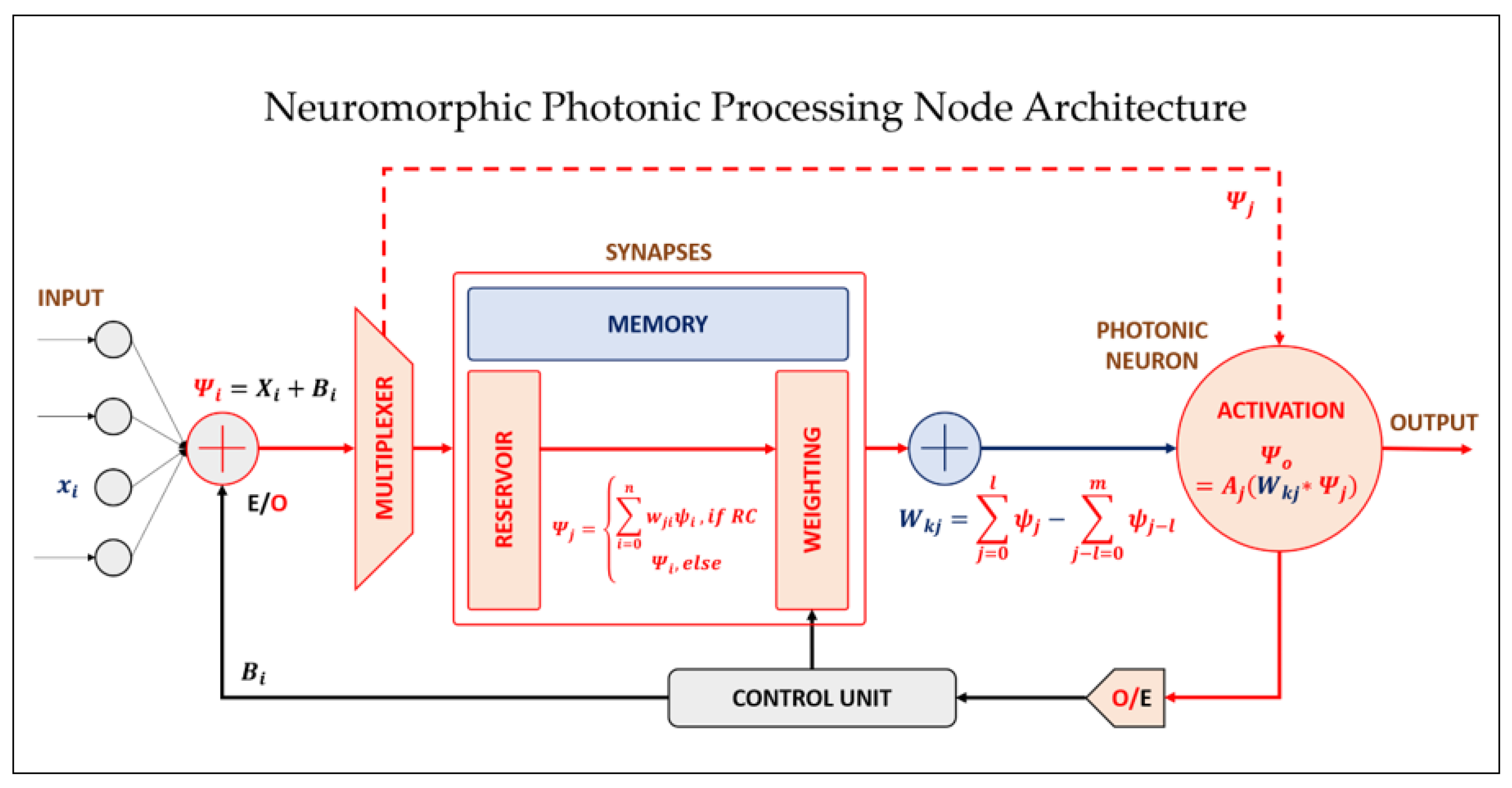
At its core, the NPPN comprises two main components: linear operation-weighting and nonlinear activation, supplemented by interconnects, memory, and photonic components. Ideal NPPN should consume minimal energy, possess high endurance, enable easy addressing in large, interconnected networks, provide signal gain and on-chip memory, and offer tunability, active dynamism, reconfigurability, and multi-functionality. Additionally, they should support large fan-in and fan-out, extensive interconnectivity, self-assembly capability, formation of 3D interconnects, and easy manufacturability in large quantities, all at low cost[57].
In the NPPN architecture (Figure 1), input signals are received as optical pulses (Ψj) from a multiplexer, representing incoming information. Optical synapses adjust the strength of connections through externally controlled feedback tuning to matrix multiply, simulating synaptic weights that may have on-chip synaptic memory (volatile or non-volatile) for storing. The weighted signals are then linearly summed (Wkj) that control PN dynamics. The PN execute the nonlinear activation, generating optical output signals (Ψo) based on modulation and interaction within the components. Moreover, the NPPN architecture exhibits similarities to an artificial neural network (ANN)[27] and reservoir computing (RC)[61] when serving as a reservoir in absence of dashed interconnects, due to the inherent parallelism supported in photonics through multiplexing. This versatility underscores the adaptability and potential of the NPPN architecture to serve as a robust platform for advanced neuromorphic computing tasks. Demonstrated NPNs utilized a variety of PN and synapses. However, one particular interest involves the creation of synapses and PN using identical technologies to facilitate seamless integration within expansive systems and enable the implementation of NN algorithms leveraging the innate physics of optical components.
2.2. Weights (Synapses): Linear Operation
Photonic synapses play a pivotal role in neuromorphic photonic computing, enabling the manipulation and processing of network signals. These synapses govern the strength of connections between neurons by assigning scalar multipliers, known as synaptic weights, to the signals transmitted across them. The weighted signals from upstream neurons are aggregated and modulated by the synaptic weights before being transmitted to downstream neurons, facilitating information and computation integration within the network. Various integrated photonic devices have been developed to implement weighted interconnection (Figure 2). These implementations can be broadly categorized into two groups based on wavelength and optical modes. However, they are not limited to and are extensively explored within the scientific community, particularly in RC. Mode-based approaches leverage interference between different optical paths and coherent input light to implement unitary matrix transforms for weighted interconnection (Figure 2a)[62]. These techniques utilize beam splitters, phase shifters, and MZIs to modulate the power and phase of light signals, enabling control over synaptic weights and interconnection matrices[39,63]. Additionally, advancements in cryogenic architectures and index-tuning mechanisms have expanded the scope of mod-based approaches (Figure 2b)[64], offering enhanced performance and flexibility in weight configuration. On the other hand, in the wavelength-based approach, signals are weighted in parallel using wavelength-division multiplexing (WDM) techniques [56] and tunable filters[48,65,66], such as MRRs[67]. These approaches, exemplified by architectures like broadcast-and-weight (B&W, Figure 2c)[48,68] and photonic cross-connect using indium phosphide (InP) semiconductor optical amplifiers (SOAs, Figure 2d)[69], although they differ in weighting mechanism, offer efficient methods for multiwavelength synapses for NPPN, with different architectures employing variations in weighted addition and attenuation mechanisms. RC uses weighted transient states of a nonlinear element with delayed feedback or time division multiplexing (TDM, Figure 2e)[70]. Non-volatile synapse implementations represent another significant advancement in neuromorphic photonic approaches (Figure 2f, g) [52,71], offering solutions that eliminate the need for electrical inputs for tuning. These approaches depend on optically induced alterations in materials like chalcogenides to regulate light propagation within waveguides. By leveraging the unique properties of non-volatile optical materials, these implementations address challenges related to electrical input/output (I/O) and heat dissipation, paving the way for more efficient and robust NPNs. A Variety of weighting mechanisms are explored[34,65,72,73,74,75,76,77] for developing weighted interconnects in neuromorphic photonics, to realizing high-performance and energy-efficient computing systems [38,56]. By leveraging the capabilities of integrated photonic circuits and novel materials, researchers are unlocking new possibilities for designing and implementing advanced NPNs with unprecedented functionality and adaptability.
2.2. Nonlinear Activation (Photonic Neuron)
PN represents a critical component to emulate the functionality of biological neurons for advanced information-processing tasks[40], which still face the challenge of achieving nonlinear activation while ensuring compatibility with network architectures, including fan-in[20] and cascadability[20]. Researchers have explored the multifaceted devices utilized for implementing PN (Figure 3 and Figure 4). Signifying two categories per the physical representation of signals: all-optical and optical/electrical/optical (O/E/O). In all-optical PN design, the neuron signal is represented solely through material properties or changes in optical susceptibilities.
While all-optical neurons offer inherent speed advantages over O/E/O implementations, they face significant challenges in achieving sufficient output strength to drive subsequent neurons. Solutions to this challenge involve integrating carrier regeneration mechanisms[85], wherein each neuron produces a renewed carrier wave modulated by its output signal, thereby enhancing its strength for downstream transmission. This approach has been demonstrated through various techniques, such as semiconductor carrier populations using cross-gain modulation (Figure 3a)[78], and structural phase transitions (Figure 3b)[44], enabling the realization of all-optical PN with enhanced functionality and cascadability. Despite introducing a new challenge of differentiating controller signals from controlled signals, carrier regeneration enables the amplification of output signals to drive downstream PN efficiently. Another avenue of exploration in PN design involves the O/E/O signal pathway, and optical signals are transduced into electrical currents and back into optical signals within the primary signal pathway (Figure 3c-g).
The nonlinear dynamics of PN using a superconducting electronic signal pathway (Figure 3c)[79,80] and a photodetector-modulator PN for MZI meshes (Figure 3d)[81] were proposed and implemented. Not only that, but this pathway enables the implementation of nonlinearities either in the electronic domain or through optical-electrical conversion stages utilizing modulators (Figure 3e, f)[82,84] or lasers (Figure 3g)[83]. By leveraging electronic components for nonlinear processing, O/E/O neurons can achieve high-bandwidth nonlinear transfer functions unconstrained by the characteristics of input signals to facilitate the generation of output signals more potent than the input essential for neural computation. Furthermore, spiking laser neurons (Figure 4), classified as all-optical or optical/electrical/optical (O/E/O), have showcased robust nonlinearity, carrier regeneration, and neural dynamics within a singular device. This is achieved by harnessing gain, cavity, and saturable processes. Spiking neurons have been demonstrated utilizing various technologies, including mode competition (Figure 4a, b)[88,89], graphene-saturable absorbers (Figure 4c)[90], saturable semiconductor media (Figure 4d, e) [91,92,95], and resonant tunneling diodes (Figure 4f)[93].
When comparing all-optical and O/E/O implementations of PN, the apparent advantage of all-optical approaches lies in their intrinsic speed, often ascribed to the comparatively sluggish carrier drift and current flow phases in O/E/O designs. However, recent developments have challenged this notion, revealing that analog O/E/O devices can exhibit comparable or even superior bandwidth and energy performance[25] compared to their all-optical counterparts. It is worth noting that in PN applying nonlinearities in the digital domain, the maximum system bandwidth is often dictated by the efficiency of the digital subsystem, underscoring the importance of efficient digital processing. Moreover, in PN design, a crucial consideration is the ability to configure and customize nonlinear transfer functions to align with specific NPN tasks. Analog PN offer flexibility in configuring transfer functions through electrical biasing[84]. Conversely, digital counterparts offer the flexibility to implement arbitrary transfer functions. Surprisingly, recent research advancements have demonstrated that programming techniques and neural training can adapt to analog photonic devices' inherent transfer functions, showcasing these devices' potential for efficient and adaptable neural computation[96,97]. Therefore, integrating PN with silicon photonics platforms holds promise for scalable and cost-effective implementation of large-scale on-chip neuromorphic photonic integrated circuits (nPIC) for information processing. Silicon photonics provide a stable ecosystem for research and development, facilitating advancements in technology road mapping, standardized fabrication processes, and broad accessibility to academic research[14]. This integration enables harnessing the scalability and feasibility of photonic integrated circuits (PIC) for realizing advanced NPNs.
3. Neuromorphic Photonic Networks
Data-centric AI-driven applications predict the urgent need for high-efficiency and ultralow power consumption solutions[98]. On-chip neuromorphic photonics has garnered attention as a complementary approach[36,99]. However, synergetic research is needed to identify optimized network topology and algorithms for NPNs[100]. ML and DL breakthroughs have propelled advancements across the hierarchy of networks, driven by various training algorithms that enable networks to adapt to diverse tasks[6,101].
Within this landscape, computational models inspired by the human brain’s structure and function, such as NNs[5,12], have gained prominence, leading to the exploration of various architectures and algorithms to enhance their capabilities. Moreover, integrating photonics into NN design has opened new avenues for achieving high-speed, wide bandwidth, energy-efficient computing supporting massive parallelism[100]. Figure 5 illustrates the evolution from essential ANNs to cutting-edge Spiking Neural Networks (SNNs) and photonic architectures, highlighting the algorithms and architectures that drive their functionality.
At the heart of ML is the concept of ANNs, computational models comprising interconnected nodes, or neurons, organized into layers. ANNs can learn complex patterns and relationships from data through a process known as training. Backpropagation, a fundamental algorithm ANNs use, adjusts synaptic weights based on the error gradient concerning each weight during training [5,102]. This iterative optimization process minimizes the difference between calculated and actual outputs, allowing the network to learn from labeled data. SNNs emulate the event-driven processing of the human brain, utilizing spikes to encode information and achieve efficient computation [44,59,103]. Neurons in SNNs integrate input spikes over time, generating output spikes when the membrane potential exceeds a threshold. This threshold-based firing mechanism, combined with spike-timing-dependent plasticity (STDP)[60], enables SNNs to learn from temporal patterns in data and exhibit robust adaptive behavior. DL represents a paradigm shift in ML, leveraging NN with multiple hidden layers to extract intricate features from raw data. Training through stochastic gradient descent (SGD) and its variants optimize the complex parameters of deep neural networks (DNN) by efficiently navigating the high-dimensional parameter space [6,104]. Convolution neural network (CNNs) are prime examples of DL architectures widely employed in image recognition and computer vision tasks[7,105]. CNNs utilize convolutional layers to detect hierarchical features in input data, then pool layers for dimensionality reduction and fully connected layers for classification. RNNs excel in sequential data by maintaining internal states or memory across time steps, making them suitable for natural language processing[9] and time-series prediction tasks[104]. RC offers a unique approach to neural network training, focusing on adapting only the readout layer while keeping the internal parameters fixed, simplifying the training process, and enhancing scalability, particularly in hardware-consertrained environments[58,70]. RC architectures, characterized by interconnected nonlinear nodes forming a fixed RNN, have shown promise in emulating complex behaviors and achieving efficient information processing.
Supervised[62], unsupervised[44], and reinforced[106] learning represent fundamental techniques in ML, each offering unique approaches to training. These methodologies provide versatile frameworks for optimizing the NN to accomplish specific tasks within various network topologies (Figure 5). Labeled data guides the NN to establish correlations between input data and corresponding output labels in supervised learning, encompassing classification [107], regression, and sequence prediction tasks. Unsupervised learning, conversely, entails training the NN on unlabeled data to unveil latent patterns or structures within the dataset, beneficial for tasks such as clustering, dimensionality reduction, and anomaly detection, enabling the extraction of meaningful representations from the data without predefined labels[44]. Reinforcement learning operates within a framework where an agent learns to navigate an environment by taking actions and receiving feedback through rewards or penalties[106]. This adaptive approach is instrumental in training NN for tasks requiring sequential decision-making, such as game-playing, robotics, and autonomous systems. As we navigate the landscape of network topologies, from ANNs and SNNs to NPNs, we witness the convergence of AI-driven technologies and cutting-edge research[99]. By embracing the complexity of NNs and harnessing the power of photonics, researchers are poised to unlock new frontiers in intelligent computing.
3.1. Neuromorphic Photonic Network: A Proposed Architecture
The NPN represents a pioneering advancement in DL architectures specifically tailored for photonic applications harnessing NPPNs as the fundamental building blocks. This innovative NN architecture integrates principles from CNNs[7,105] and RNNs[102,108], leveraging the unique properties of light for efficient computation. The network consists of two primary components: convolutional layers with activation functions followed by pooling layers and a recurrent feedback loop. The architecture is structured to exploit spatial and temporal correlations in input data, making it well-suited but not limited to tasks such as pattern recognition, classification, and sequential data processing.
A proposed approach to recurrent convolutional neuromorphic photonic networks (RecConv-nPN, Figure 5):
- Instead of traditional convolutional layers, the RecConv-nPN employs NPPNs to perform convolutional operations directly on input photonic signals, enabling them to extract spatial features from the input data and apply nonlinear activation functions simultaneously.
- NPPNs in RC mode, followed by unit weighting within the synapse for pooling operations (Figure 1), eliminating the need for different variety of layers. NPPNs dynamically aggregate information across spatial dimensions of the input data, facilitating down sampling and feature selection while preserving the advantages of photonic processing.
- A defining feature of the RecConv-nPN is its incorporation of a recurrent feedback loop enabled by the inherent memory (synaptic or delayed) properties of NPPNs. The output from the post NPPNs is fed back into the pre NPPNs in the network, allowing for iterative refinement of representations over multiple time steps and capturing temporal dependencies in the input data.
- Following the recurrent processing stage, the output is flattened for processing (say classification). This final layer utilizes standard classification techniques to map the learned features to specific output classes, enabling the network to make accurate predictions based on the input data.
3.1. Neuromorphic Photonic Approaches
State-of-the-art neuromorphic photonic approaches represent AI, leveraging the principles of neuroscience and photonics to develop energy-efficient and high-performance computing systems. Various NPNs proposed and experimentally demonstrated (Figure 6) the potential across different architectures. These approaches encompass different topologies (NPNs), weighting (synapse), and photonic signal representations (PN). Each approach offers unique achievements and challenges, paving the way for innovative solutions in neuromorphic computing (Table 1, Remarks). Solutions to the challenges of these approaches are promising for revolutionizing computing paradigms and enabling advanced AI applications in various domains.
RC leverages the complex dynamics of optical systems to perform computation. By utilizing interconnected delays between the fixed nonlinear nodes with multiple feedback loops, RC architectures demonstrate remarkable capabilities in emulating complex behaviours and processing information efficiently (Figure 6a)[61]. Recent advancements in RC have focused on integrating passive photonic elements, such as waveguides and resonators, to achieve scalable and high-performance computing[109]. Experimental demonstrations have showcased the ability of photonic RC to perform application-specific tasks such as spoken digit recognition, time-series prediction, and signal optimization, making it a promising candidate for various real-world applications[70,110].
Superconducting optoelectronic circuits (SOC) combine the advantages of superconducting electronics and photonics to achieve ultrafast and energy-efficient computing optimized for scalability (Figure 6b)[111]. These circuits exploit the superconducting nanowires, single-photon detectors, and capacitive micro-electromechanical system (MEMS)-based modulators to perform unprecedentedly efficient NN operations on a chip, paving the way for scalable and high-performance neuromorphic computing platforms with an energy cost associated with cooling at cryogenic temperature necessary for operation[64,80,112]. The MZI-based coherent nanophotonic circuits (CNC) leverage coherent light manipulation to perform complex computational tasks (Figure 6c)[62]. Integrating beamsplitters and phase shifters enables these circuits to control optical signals and facilitate high-speed processing, but they are bulky and require high driving voltages[39,63,81]. Experimental demonstrations have shown the potential of CNC for implementing neuromorphic algorithms such as in situ backpropagation[27], self-calibration[96], and asymptotically fault-tolerant programable photonic circuits[97], opening new avenues for ultrafast and energy-efficient computing[113,114,115].
Broadcast and weight networks (B&W) utilize the concept of WDM to perform matrix-vector multiplication efficiently (Figure 6d)[102]. These networks can achieve parallel processing of NN operations by modulating optical signals at specific wavelengths and tuning MRRs[48,66,116]. Experimental implementations have demonstrated its scalability and energy efficiency for solving differential equations, making them promising candidates for nPIC for computing[68,84].
Multiwavelength photonic neurosynaptic networks (MN) integrate PCM-germanium-antimony-tellurium(GST)- based PN (Figure 6e) [44] and synapses[52] on silicon nitride on a silicon dioxide platform with inherent synaptic memory associated with PCM with no energy requirement to maintain its states in case of offline learning. Online learning can be challenging, with individual PCM devices' endurance of 10 switching cycles requiring and requiring nJ of energy per cycle. These networks leverage the optical mode in a controlled manner to perform complex cognitive tasks. Experimental demonstrations have shown the feasibility of implementing MN for tasks such as pattern recognition and associative memory with supervised and unsupervised learning, highlighting their potential for next-generation nPIC [104,105]. On-chip diffractive neural networks (DO) harness the principles of diffractive optics to perform computational operations passively. By integrating diffractive elements in silicon slots filled with silicon dioxide (SSSD), these networks can achieve parallel processing of optical signals with minimal power consumption (Figure 6f)[107]. Experimental implementations have demonstrated the ability of DO to perform image classification[107,115].
3.1. Algorithms and Methods for Training Neuromorphic Photonic Networks
NPNs represent a burgeoning frontier ripe with promise. However, training algorithms face unique challenges due to the nonlinear nature of optical components and the need for efficient optimization techniques for a delicate balance between processing and memory access[99,100]. Unlike conventional AI algorithms deployed in software applications, developing customized training algorithms tailored for photonic hardware implementation could herald a transformative shift in this domain (Table 2). One of the key challenges in training NPNs lies in achieving precision (Table 2, Networks and Training). Traditional backpropagation algorithms, which are highly effective for training deep AI networks, require precise adjustments of weights based on slight variations in error gradients. However, most nanodevices used in NPN are inherently noisy, making it challenging to achieve such fine adjustments. Novel training algorithms that can adapt to the imperfections and variability of physical devices can cash on the inherent properties of photonics. Several strategies are proposed to address the precision challenge in photonic training, including the photonic generative network that harnesses noises of photonic hardware[117], a heuristic photonic recurrent algorithm for the Ising problem[118], and the photonic analog of the backpropagation leveraging adjoint variable methods that can significantly reduce complexity by simplifying the mathematical model associated with training[27] algorithm. Additionally, statistical optimization tools, including genetic algorithms[119], Bayesian optimization[120], nonlinearity inversion[108], and equilibrium propagation[121], have been investigated for optimizing weights in NPNs. These gradient-free algorithms show promise for training NPNs efficiently, particularly for classification tasks with different datasets[122]. Another essential consideration in NPN training is the need for weight-independent variations using external signals (electrical or optical). Furthermore, modifying existing algorithms to work effectively despite device imperfections is crucial, as demonstrated in self-calibrated[96] and asymptotically fault-tolerant[97] programmable NPNs. Unsupervised learning algorithms are particularly intriguing for NPNs and are highly adaptable to device imperfections. STDP is a popular unsupervised learning rule inspired by neuroscience[106]. In STDP, synaptic weights are
modified based on the temporal relationship between pre-synaptic and post-synaptic activities, making it suitable for implementation in NPNs (Table 2, Networks and Training)[44,111]. In addition to precision and unsupervised learning, optimizing nPIC presents challenges. Mitigating the complexity of probing local optical intensities across the circuit is essential for efficient training. Recent advancements propose on-chip reconfigurable[126] and control-free hardware-aware[122] training for NPNs. In contrast, Boolean learning via coordinate descent offers a practical and efficient alternative to error backpropagation[106], enabling high-performance NPNs with programmable connections. These novel training schemes (Table 2), proposed or experimentally validated for NPNs, underscore a dynamic landscape characterized by notable achievements, persistent challenges, and promising prospects also highlighted in state-of-the-art NPN demonstrations[104,123,124,125]. By addressing the challenges and exploring innovative training algorithms, NPNs hold the potential to revolutionize neuromorphic computing paradigms, offering energy-efficient and high-performance solutions for a wide range of applications (Figure 7).
4. Discussion
The demand for AI and its multifaceted applications is accelerating rapidly, exemplified by recent advancements such as DALL-E3 and Sora[53], which require massive computational power for training models with billions of parameters. Such tasks have relied on large-scale clusters of accelerators like GPUs or TPUs[98]. Neuromorphic photonics holds the potential to support these power-hungry processors, particularly for ASIC demands. Photonics leverage its inherent bandwidth, parallelism [20], picosecond latencies[25], and energy efficiency (measured in pJ/FLOP)[3]. Mainstream silicon photonic platforms offer a fundamental device library encompassing modulators, waveguides, and detectors, crucial for constructing signal pathways within diverse neuromorphic architectures. Innovations in conventional manufacturing processes, including the integration of PCMs and superconducting electronics, are being investigated to broaden the range of achievable architectures [45,46,47].
4.1. Exploring the Current State-of-the-Art: Challenges and Solutions
- a.
- Synergistic Co-the integration of Photonics with Electronics
Silicon photonics has its advantages but still faces challenges yet to be solved. Coherent on-chip architectures utilizing components like MZIs are susceptible to thermal and fabrication processes, leading to variations in phase, interference, and diffraction. This results in inaccuracies in NPNs, emphasizing the need for strategies to mitigate these effects during training and tuning. Non-coherent architectures face challenges such as heterodyne crosstalk in MRRs and the requirement for numerous modulation resources, limiting scalability and energy efficiency. Efforts to address these challenges include exploring parallel arrangements of MRRs, leveraging microdisks, and facilitating increased integration density on-chip. Variations and reliability issues also present significant hurdles in silicon photonic devices, affecting their performance and stability. Therefore, electronic controllers for feedback and algorithm (calibration), direct current analog signal for biasing, analog to digital, and digital to analog for trans-impedance amplification pose a solution in managing photonic devices and ensuring the stable operation of NPNs. However, high latencies and frequency mismatches between electronic controllers and optical networks pose real-time, high-speed operation challenges.
Thus, integrating on-chip active electronics becomes crucial, and a significant challenge is the need for more complex on-chip electronic circuitry, which demands a higher density of electrical ports than optical ports, with the number of electrical ports scaling quadratically with the optical ports. Despite the challenges, the co-integration of CMOS electronics and photonics holds promise for overcoming many limitations by leveraging the advantages of both technologies while mitigating their drawbacks. Technologies including flip-chip bonding, wirebonding, and monolithic fabrication enable the integration of CMOS electronics optimized for digital control with silicon photonic chips[45,47], offering advantages such as increased interconnection density and reduced parasitic impedance.
- b.
- On-chip Light Sources on Silicon Platform
Power efficiency is critical in neuromorphic photonics, with O/E/O conversions consuming considerable power. At the same time, all-optical neurons offer better power efficiency. Additionally, off-chip lasers contribute significantly to power consumption, necessitating research into power-efficient on-chip light sources. Efforts to tackle this challenge involve integrating light sources directly onto the silicon waveguide layer[127], employing methods such as rare-earth-element doping, strain engineering of germanium, and all-silicon emissive defects[80]. This is advantageous as it eliminates the need to send the optical signal off-chip for computation, which is particularly beneficial for neuromorphic photonics systems employing NPNs. The selection of lasers for neuromorphic photonics depends on the type of neuron involved. Multi-die techniques are applicable for systems utilizing modulator-class neurons, where the light source can be positioned outside the chip. However, precise integration of optical gain onto waveguides is essential for laser-class neurons.
4.2. Advancements and Future Directions in Scientific Inquiry
- b.
- Fabrication Challenges
An essential aspect of advancing neuromorphic photonics involves enhancing the robustness of systems to environmental fluctuations and overcoming fabrication challenges. Analog circuits, typical in neuromorphic processors, often require trimming to address manufacturing variabilities and environmental sensitivities. In integrated photonics, resonant devices like MRRs pose challenges due to their sensitivity to variations[67]. One approach to mitigate these challenges is resonance trimming, which involves inducing changes in the refractive index of waveguides. Active trimming methods, including heating waveguides to environmental variability, require constant power input and fast response times. Alternatively, passive trimming methods utilize permanent or non-volatile techniques to adjust the refractive index of devices. These methods, including electron-beam-induced compaction[128] and strain of oxide cladding[129], offer solutions for correcting fabrication variations or preprogramming circuits to default states. Moreover, the integration of field-programmable PCMs allows for in-place reconfiguration[51], further enhancing robustness to fabrication discrepancies. In addition to addressing variability, advancements in neuromorphic photonics necessitate the development of analog-aware compilers to map application tasks to photonic hardware effectively[130]. Unlike traditional compilers for electronic systems, photonic compilers must account for idiosyncrasies inherent in representing signals in WDM lightwaves, including nonlinear distortion and limited dynamic range. Collaborative efforts within the academic community are underway to develop these compilers tailored for neuromorphic and programmable photonics[28,37,62,96,131], enabling efficient task mapping and optimization for photonic systems. By addressing these challenges and embracing innovative solutions, the field of neuromorphic photonics can enhance its resilience to environmental fluctuations and fabrication complexities, thereby facilitating the realization of robust and reliable neuromorphic computing systems.
- c.
- Integration of Photonic Components
Efficient interfacing of analog processors with photonic hardware requires the development of photonic digital-to-analog converters (DACs) to avoid costly conversions, including digital-to-analog conversion and electro-optic modulation. DACs facilitate high sampling rates, precision, and low distortion while exhibiting reduced susceptibility to electromagnetic noise compared to their electronic counterparts. Photonic DACs can be realized through various methods, including optical intensity weighting of multiwavelength signals modulated with silicon MRRs incorporating depletion-mode PN junctions[132]. Another approach utilizes silicon-on-insulator traveling-wave multi-electrode Mach-Zehnder modulators [133]. Integrating photonic DACs enables the seamless conversion of digital signals to analog photonic signals, facilitating the implementation of advanced functionalities.
Advancements in tailored light sources hold immense potential for pushing the boundaries of neuromorphic photonics. Current efforts focus on developing chip-scale frequency combs utilizing soliton microcombs, a breakthrough achieved through CMOS-compatible PIC. By leveraging resonators designed to compensate for dispersion, these microcombs generate stable and broadband frequency combs with precisely aligned wavelengths, ideal for generating tailored input signals in parallel from a single source[41]. Moreover, the advent of lithium niobate-on-insulator modulators signifies a substantial advancement in photonic chip design, providing compatibility with silicon photonic devices and facilitating the integration of fast electro-optical modulators and efficient nonlinear optical elements on the same chip. These modulators feature high modulation frequencies and low voltage–length products, thereby reducing energy consumption and device footprint in nPIC[134].
- c.
- Synaptic Memory
The integration of synaptic memory stands out as a critical area of exploration. Conventional approaches have typically depended on a blend of specialized photonic devices controlled by generalized electronic circuits. However, the absence of standard building blocks like high-level compilers, logic gates, and memory within current photonic platforms necessitates innovative strategies to incorporate memory into neuromorphic processors effectively. For specific ML and neuromorphic applications, such as DL inference, synaptic weights, once trained, may not require frequent updates. In these scenarios, non-volatile analog memory, such as in-memory computing utilizing PCMs, presents a promising solution[50,135]. By interfacing with digital electronic drivers, these memory systems enable real-time NN operation, precomputed weight storage, and direct inference task execution on the hardware[105]. Nevertheless, challenges persist in scenarios where temporary storage of neuron outputs is required, as seen in long short-term memory RNN. In such cases, alternative memory technologies, including digital or short-term analogue electronic memory with electro-optic interfaces to analog photonics, may be better suited. While analog memory may exhibit limitations in precision and noise compared to digital memory, recent studies have shown that even low precision can support effective deep RNN operations. As neuromorphic photonics progress, they are expected to adopt heterogeneous memory technologies, akin to modern computers, comprising various memory types within a single system[131,136]. This evolution may involve integrating electronic memory components alongside novel photonic memory technologies, offering non-volatile and reconfigurable capabilities essential for dynamic neural network operations.
4.2. Envisioning the Future of Neuromorphic Photonics: A Visionary Perspective
Neuromorphic photonics represents a fusion of advanced technologies and innovative architectural designs pivotal for constructing NNs. A prominent concept, the NPP [36], embodies this integration by leveraging state-of-the-art photonic packaging and emerging integrated photonics. The NPP seamlessly merges optical and electronic components within a system-in-package framework, enabling versatile signal processing and control functionalities. Here we deal two fundamental architectures, the NPPN, and the RecConv-nPN, as contributions to the evolving field of neuromorphic photonics, offering blueprints for realizing large-scale NNs. The convergence of photonics and neuromorphic computing signifies a transformative era of technological advancement and scientific exploration. Embracing perspectives and pioneering research endeavors will unlock the vast potential of neuromorphic photonics, reshaping the landscape of on-chip neuromorphic computing for application-specific AI.
5. Conclusion
Neuromorphic photonics basing its foot in photonic Integrated circuits represent a transformative approach to optoelectronic (grabbing the lower-hanging fruit first) or all-optical (too early to demand, requires technological advancement) hardware design, aiming to create systems that mirror the structure and functionality of NNs. This isomorphic relationship between NPNs and their biological counterparts promises remarkable capabilities and has sparked significant technological and societal interest. Over recent years, research in NPNs has witnessed rapid growth, leading to the exploration of diverse architectural concepts, PN models, training techniques, and network topologies. This diversity highlights the dynamic nature of the field, with ongoing efforts aimed at identifying optimal applications where photonics can outperform traditional electronic computing methods. Real-time applications requiring rapid decision-making are particularly promising arenas for deploying neuromorphic photonics. A key focus will be on scaling the integration of PN within single networks. Despite challenges such as the co-packaging of control electronics and light sources, advancements in scalable photonics platforms offer promising avenues for overcoming these obstacles. With modern integrated platforms and innovative ideas and devices for on-chip functionality, neuromorphic photonics is poised to push the boundaries of ML and information processing, unlocking new frontiers in AI and computational capabilities.
Author Contributions
All Authors contributed equally to the manuscript. All the authors have accepted the responsibility for the entire content of this submitted manuscript and approved submission. All authors have read and agreed to the published version of the manuscript.
Funding
Not applicable.
Institutional Review Board Statement
Not applicable.
Informed Consent Statement
Not applicable.
Data Availability Statement
Not applicable.
Acknowledgments
SG gratefully acknowledges the PhD research supporting award of the INSPIRE Fellowship [DST/INSPIRE/03/2021/001134] from the Department of Science and Technology, India.
Conflicts of Interest
The authors declare no conflict of interest.
References
- Batra. Gaurav; Jacobson, Z.; Madhav, S.; Queirolo, A.; Santhanam, N. Artificial-Intelligence Hardware: New Opportunities for Semiconductor Companies, High Tech, Dec. 2018.
- Rosenblatt, F. The Perceptron, a Perceiving and Recognizing Automaton Project Para; Cornell Aeronautical Laboratory, 1957;
- Nahmias, M.A.; de Lima, T.F.; Tait, A.N.; Peng, H.-T.; Shastri, B.J.; Prucnal, P.R. Photonic Multiply-Accumulate Operations for Neural Networks. IEEE Journal of Selected Topics in Quantum Electronics 2020, 26, 1–18. [Google Scholar] [CrossRef]
- Wetzstein, G.; Ozcan, A.; Gigan, S.; Fan, S.; Englund, D.; Soljačić, M.; Denz, C.; Miller, D.A.B.; Psaltis, D. Inference in Artificial Intelligence with Deep Optics and Photonics. Nature 2020, 588, 39–47. [Google Scholar] [CrossRef] [PubMed]
- Rumelhart, D.E.; Hinton, G.E.; Williams, R.J. Learning Representations by Back-Propagating Errors. Nature 1986, 323, 533–536. [Google Scholar] [CrossRef]
- LeCun, Y.; Bengio, Y.; Hinton, G. Deep Learning. Nature 2015, 521, 436–444. [Google Scholar] [CrossRef]
- Li, Z.; Liu, F.; Yang, W.; Peng, S.; Zhou, J. A Survey of Convolutional Neural Networks: Analysis, Applications, and Prospects. IEEE Trans Neural Netw Learn Syst 2022, 33, 6999–7019. [Google Scholar] [CrossRef]
- Choquette, J. NVIDIA Hopper H100 GPU: Scaling Performance. IEEE Micro 2023, 43, 9–17. [Google Scholar] [CrossRef]
- Yonghui Wu; Mike Schuster; Zhifeng Chen; Quoc V. Le; Mohammad Norouzi; Wolfgang Macherey Google’s Neural Machine Translation System: Bridging the Gap between Human and Machine Translation. arXiv preprint arXiv:1609.08144 2016, arXiv:1609.08144 2016.
- Huang, C.; Sorger, V.J.; Miscuglio, M.; Al-Qadasi, M.; Mukherjee, A.; Lampe, L.; Nichols, M.; Tait, A.N.; Ferreira de Lima, T.; Marquez, B.A.; et al. Prospects and Applications of Photonic Neural Networks. Adv Phys X 2022, 7. [Google Scholar] [CrossRef]
- LeCun, Y.; Boser, B.; Denker, J.; Henderson, D.; Howard, R.; Hubbard, W.; Jackel, L. Handwritten Digit Recognition with a Back-Propagation Network. Adv Neural Inf Process Syst 1989, 2. [Google Scholar]
- Hinton, G.E.; Salakhutdinov, R.R. Reducing the Dimensionality of Data with Neural Networks. Science (1979) 2006, 313, 504–507. [Google Scholar] [CrossRef]
- Capper, D.; Jones, D.T.W.; Sill, M.; Hovestadt, V.; Schrimpf, D.; Sturm, D.; Koelsche, C.; Sahm, F.; Chavez, L.; Reuss, D.E.; et al. DNA Methylation-Based Classification of Central Nervous System Tumours. Nature 2018, 555, 469–474. [Google Scholar] [CrossRef] [PubMed]
- Shekhar, S.; Bogaerts, W.; Chrostowski, L.; Bowers, J.E.; Hochberg, M.; Soref, R.; Shastri, B.J. Roadmapping the next Generation of Silicon Photonics. Nat Commun 2024, 15, 751. [Google Scholar] [CrossRef] [PubMed]
- Berggren, K.; Xia, Q.; Likharev, K.K.; Strukov, D.B.; Jiang, H.; Mikolajick, T.; Querlioz, D.; Salinga, M.; Erickson, J.R.; Pi, S.; et al. Roadmap on Emerging Hardware and Technology for Machine Learning. Nanotechnology 2021, 32, 012002. [Google Scholar] [CrossRef] [PubMed]
- Merolla, P.A.; Arthur, J. V.; Alvarez-Icaza, R.; Cassidy, A.S.; Sawada, J.; Akopyan, F.; Jackson, B.L.; Imam, N.; Guo, C.; Nakamura, Y.; et al. A Million Spiking-Neuron Integrated Circuit with a Scalable Communication Network and Interface. Science (1979) 2014, 345, 668–673. [Google Scholar] [CrossRef]
- Furber, S.B.; Galluppi, F.; Temple, S.; Plana, L.A. The SpiNNaker Project. Proceedings of the IEEE 2014, 102, 652–665. [Google Scholar] [CrossRef]
- Davies, M.; Srinivasa, N.; Lin, T.-H.; Chinya, G.; Cao, Y.; Choday, S.H.; Dimou, G.; Joshi, P.; Imam, N.; Jain, S.; et al. Loihi: A Neuromorphic Manycore Processor with On-Chip Learning. IEEE Micro 2018, 38, 82–99. [Google Scholar] [CrossRef]
- Benjamin, B.V.; Gao, P.; McQuinn, E.; Choudhary, S.; Chandrasekaran, A.R.; Bussat, J.-M.; Alvarez-Icaza, R.; Arthur, J. V.; Merolla, P.A.; Boahen, K. Neurogrid: A Mixed-Analog-Digital Multichip System for Large-Scale Neural Simulations. Proceedings of the IEEE 2014, 102, 699–716. [Google Scholar] [CrossRef]
- Goodman, J.W. Fan-in and Fan-out with Optical Interconnections. Optica Acta: International Journal of Optics 1985, 32, 1489–1496. [Google Scholar] [CrossRef]
- Sawada, J.; Akopyan, F.; Cassidy, A.S.; Taba, B.; Debole, M. V.; Datta, P.; Alvarez-Icaza, R.; Amir, A.; Arthur, J. V.; Andreopoulos, A.; et al. TrueNorth Ecosystem for Brain-Inspired Computing: Scalable Systems, Software, and Applications. In Proceedings of the SC16: International Conference for High Performance Computing, Networking, Storage and Analysis; IEEE, November 2016; pp. 130–141.
- Pei, J.; Deng, L.; Song, S.; Zhao, M.; Zhang, Y.; Wu, S.; Wang, G.; Zou, Z.; Wu, Z.; He, W.; et al. Towards Artificial General Intelligence with Hybrid Tianjic Chip Architecture. Nature 2019, 572, 106–111. [Google Scholar] [CrossRef]
- Jake Siegel With a Systems Approach to Chips, Microsoft Aims to Tailor Everything ‘from Silicon to Service’ to Meet AI Demand.
- Miller, D.A.B. Rationale and Challenges for Optical Interconnects to Electronic Chips. Proceedings of the IEEE 2000, 88, 728–749. [Google Scholar] [CrossRef]
- Nozaki, K.; Matsuo, S.; Fujii, T.; Takeda, K.; Shinya, A.; Kuramochi, E.; Notomi, M. Femtofarad Optoelectronic Integration Demonstrating Energy-Saving Signal Conversion and Nonlinear Functions. Nat Photonics 2019, 13, 454–459. [Google Scholar] [CrossRef]
- Han, J.; Jentzen, A.; E, W. Solving High-Dimensional Partial Differential Equations Using Deep Learning. Proceedings of the National Academy of Sciences 2018, 115, 8505–8510. [Google Scholar] [CrossRef] [PubMed]
- Hughes, T.W.; Minkov, M.; Shi, Y.; Fan, S. Training of Photonic Neural Networks through in Situ Backpropagation and Gradient Measurement. Optica 2018, 5, 864. [Google Scholar] [CrossRef]
- Tait, A.N.; Ma, P.Y.; Ferreira de Lima, T.; Blow, E.C.; Chang, M.P.; Nahmias, M.A.; Shastri, B.J.; Prucnal, P.R. Demonstration of Multivariate Photonics: Blind Dimensionality Reduction With Integrated Photonics. Journal of Lightwave Technology 2019, 37, 5996–6006. [Google Scholar] [CrossRef]
- Markram, H. The Human Brain Project. Sci Am 2012, 306, 50–55. [Google Scholar] [CrossRef]
- Josh Achiam; Steven Adler; Sandhini Agarwal; Lama Ahmad; Ilge Akkaya; et. al. GPT-4 Technical Report. ArXiv 2023, 1–100.
- Tesla Dojo Technology A Guide to Tesla’s Configurable Floating Point Formats & Arithmetic. Available online: https://digitalassets.tesla.com/tesla-contents/image/upload/tesla-dojo-technology.pdf (accessed on 1 March 2024).
- Goodman, J.W.; Dias, A.R.; Woody, L.M. Fully Parallel, High-Speed Incoherent Optical Method for Performing Discrete Fourier Transforms. Opt Lett 1978, 2, 1. [Google Scholar] [CrossRef]
- Keyes, R.W. Optical Logic-in the Light of Computer Technology. Optica Acta: International Journal of Optics 1985, 32, 525–535. [Google Scholar] [CrossRef]
- Patel, D.; Ghosh, S.; Chagnon, M.; Samani, A.; Veerasubramanian, V.; Osman, M.; Plant, D. V. Design, Analysis, and Transmission System Performance of a 41 GHz Silicon Photonic Modulator. Opt Express 2015, 23, 14263. [Google Scholar] [CrossRef]
- Argyris, A. Photonic Neuromorphic Technologies in Optical Communications. Nanophotonics 2022, 11, 897–916. [Google Scholar] [CrossRef]
- Shastri, B.J.; Tait, A.N.; Ferreira de Lima, T.; Pernice, W.H.P.; Bhaskaran, H.; Wright, C.D.; Prucnal, P.R. Photonics for Artificial Intelligence and Neuromorphic Computing. Nat Photonics 2021, 15, 102–114. [Google Scholar] [CrossRef]
- Nahmias, M.A.; Shastri, B.J.; Tait, A.N.; Ferreira De Lima, T.; Prucnal, P.R. Neuromorphic Photonics; 2018.
- Zhou, H.; Dong, J.; Cheng, J.; Dong, W.; Huang, C.; Shen, Y.; Zhang, Q.; Gu, M.; Qian, C.; Chen, H.; et al. Photonic Matrix Multiplication Lights up Photonic Accelerator and Beyond. Light Sci Appl 2022, 11. [Google Scholar] [CrossRef] [PubMed]
- Carolan, J.; Harrold, C.; Sparrow, C.; Martín-López, E.; Russell, N.J.; Silverstone, J.W.; Shadbolt, P.J.; Matsuda, N.; Oguma, M.; Itoh, M.; et al. Universal Linear Optics. Science (1979) 2015, 349, 711–716. [Google Scholar] [CrossRef] [PubMed]
- Maryam Moridsadat; Marcus Tamura; Lukas Chrostowski; Sudip Shekhar; Bhavin J. Shastri Design Methodology for Silicon Organic Hybrid Modulators: From Physics to System-Level Modeling. ArXiv 2024, 1–16.
- Gaeta, A.L.; Lipson, M.; Kippenberg, T.J. Photonic-Chip-Based Frequency Combs. Nat Photonics 2019, 13, 158–169. [Google Scholar] [CrossRef]
- Xavier, J.; Probst, J.; Becker, C. Deterministic Composite Nanophotonic Lattices in Large Area for Broadband Applications. Sci Rep 2016, 6. [Google Scholar] [CrossRef]
- Xavier, J.; Probst, J.; Back, F.; Wyss, P.; Eisenhauer, D.; Löchel, B.; Rudigier-Voigt, E.; Becker, C. Quasicrystalline-Structured Light Harvesting Nanophotonic Silicon Films on Nanoimprinted Glass for Ultra-Thin Photovoltaics. Opt Mater Express 2014, 4, 2290. [Google Scholar] [CrossRef]
- Feldmann, J.; Youngblood, N.; Wright, C.D.; Bhaskaran, H.; Pernice, W.H.P. All-Optical Spiking Neurosynaptic Networks with Self-Learning Capabilities. Nature 2019, 569, 208–214. [Google Scholar] [CrossRef]
- Stojanović, V.; Ram, R.J.; Popović, M.; Lin, S.; Moazeni, S.; Wade, M.; Sun, C.; Alloatti, L.; Atabaki, A.; Pavanello, F.; et al. Monolithic Silicon-Photonic Platforms in State-of-the-Art CMOS SOI Processes [Invited]. Opt Express 2018, 26, 13106. [Google Scholar] [CrossRef]
- Sun, C.; Wade, M.T.; Lee, Y.; Orcutt, J.S.; Alloatti, L.; Georgas, M.S.; Waterman, A.S.; Shainline, J.M.; Avizienis, R.R.; Lin, S.; et al. Single-Chip Microprocessor That Communicates Directly Using Light. Nature 2015, 528, 534–538. [Google Scholar] [CrossRef]
- Bogaerts, W.; Chrostowski, L. Silicon Photonics Circuit Design: Methods, Tools and Challenges. Laser Photon Rev 2018, 12. [Google Scholar] [CrossRef]
- Tait, A.N.; De Lima, T.F.; Nahmias, M.A.; Shastri, B.J.; Prucnal, P.R. Continuous Calibration of Microring Weights for Analog Optical Networks. IEEE Photonics Technology Letters 2016, 28, 887–890. [Google Scholar] [CrossRef]
- de Lima, T.F.; Peng, H.-T.; Tait, A.N.; Nahmias, M.A.; Miller, H.B.; Shastri, B.J.; Prucnal, P.R. Machine Learning With Neuromorphic Photonics. Journal of Lightwave Technology 2019, 37, 1515–1534. [Google Scholar] [CrossRef]
- Ríos, C.; Youngblood, N.; Cheng, Z.; Le Gallo, M.; Pernice, W.H.P.; Wright, C.D.; Sebastian, A.; Bhaskaran, H. In-Memory Computing on a Photonic Platform. Sci Adv 2019, 5. [Google Scholar] [CrossRef] [PubMed]
- Rios, C.; Stegmaier, M.; Hosseini, P.; Wang, D.; Scherer, T.; Wright, C.D.; Bhaskaran, H.; Pernice, W.H.P. Integrated All-Photonic Non-Volatile Multi-Level Memory. Nat Photonics 2015, 9, 725–732. [Google Scholar] [CrossRef]
- Cheng, Z.; Ríos, C.; Pernice, W.H.P.; Wright, C.D.; Bhaskaran, H. On-Chip Photonic Synapse. Sci Adv 2017, 3. [Google Scholar] [CrossRef]
- James Betker; Gabriel Goh; Li Jing; Tim Brooks; Jianfeng Wang; Linjie Li; Long Ouyang; Juntang Zhuang; Joyce Lee; Yufei Guo; et al. Improving Image Generation with Better Captions. Available online: https://cdn.openai.com/papers/dall-e-3.pdf (accessed on 25 February 2024).
- Xu, B.; Huang, Y.; Fang, Y.; Wang, Z.; Yu, S.; Xu, R. Recent Progress of Neuromorphic Computing Based on Silicon Photonics: Electronic–Photonic Co-Design, Device, and Architecture. Photonics 2022, 9. [Google Scholar] [CrossRef]
- Farhat, N.H.; Psaltis, D.; Prata, A.; Paek, E. Optical Implementation of the Hopfield Model. Appl Opt 1985, 24, 1469. [Google Scholar] [CrossRef]
- Bai, Y.; Xu, X.; Tan, M.; Sun, Y.; Li, Y.; Wu, J.; Morandotti, R.; Mitchell, A.; Xu, K.; Moss, D.J. Photonic Multiplexing Techniques for Neuromorphic Computing. Nanophotonics 2023, 12, 795–817. [Google Scholar] [CrossRef]
- Marković, D.; Mizrahi, A.; Querlioz, D.; Grollier, J. Physics for Neuromorphic Computing. Nature Reviews Physics 2020, 2, 499–510. [Google Scholar] [CrossRef]
- Jaeger, H.; Haas, H. Harnessing Nonlinearity: Predicting Chaotic Systems and Saving Energy in Wireless Communication. Science (1979) 2004, 304, 78–80. [Google Scholar] [CrossRef] [PubMed]
- Maass, W. Networks of Spiking Neurons: The Third Generation of Neural Network Models. Neural Networks 1997, 10, 1659–1671. [Google Scholar] [CrossRef]
- Song, S.; Miller, K.D.; Abbott, L.F. Competitive Hebbian Learning through Spike-Timing-Dependent Synaptic Plasticity. Nat Neurosci 2000, 3, 919–926. [Google Scholar] [CrossRef] [PubMed]
- Vandoorne, K.; Mechet, P.; Van Vaerenbergh, T.; Fiers, M.; Morthier, G.; Verstraeten, D.; Schrauwen, B.; Dambre, J.; Bienstman, P. Experimental Demonstration of Reservoir Computing on a Silicon Photonics Chip. Nat Commun 2014, 5. [Google Scholar] [CrossRef]
- Shen, Y.; Harris, N.C.; Skirlo, S.; Prabhu, M.; Baehr-Jones, T.; Hochberg, M.; Sun, X.; Zhao, S.; Larochelle, H.; Englund, D.; et al. Deep Learning with Coherent Nanophotonic Circuits. Nat Photonics 2017, 11, 441–446. [Google Scholar] [CrossRef]
- Reck, M.; Zeilinger, A.; Bernstein, H.J.; Bertani, P. Experimental Realization of Any Discrete Unitary Operator. Phys Rev Lett 1994, 73, 58–61. [Google Scholar] [CrossRef]
- Chiles, J.; Buckley, S.M.; Nam, S.W.; Mirin, R.P.; Shainline, J.M. Design, Fabrication, and Metrology of 10 × 100 Multi-Planar Integrated Photonic Routing Manifolds for Neural Networks. APL Photonics 2018, 3. [Google Scholar] [CrossRef]
- Jayatilleka, H.; Murray, K.; Guillén-Torres, M.Á.; Caverley, M.; Hu, R.; Jaeger, N.A.F.; Chrostowski, L.; Shekhar, S. Wavelength Tuning and Stabilization of Microring-Based Filters Using Silicon in-Resonator Photoconductive Heaters. Opt Express 2015, 23, 25084. [Google Scholar] [CrossRef]
- Tait, A.N.; Jayatilleka, H.; De Lima, T.F.; Ma, P.Y.; Nahmias, M.A.; Shastri, B.J.; Shekhar, S.; Chrostowski, L.; Prucnal, P.R. Feedback Control for Microring Weight Banks. Opt Express 2018, 26, 26422. [Google Scholar] [CrossRef]
- Bogaerts, W.; De Heyn, P.; Van Vaerenbergh, T.; De Vos, K.; Kumar Selvaraja, S.; Claes, T.; Dumon, P.; Bienstman, P.; Van Thourhout, D.; Baets, R. Silicon Microring Resonators. Laser Photon Rev 2012, 6, 47–73. [Google Scholar] [CrossRef]
- Tait, A.N.; Wu, A.X.; De Lima, T.F.; Zhou, E.; Shastri, B.J.; Nahmias, M.A.; Prucnal, P.R. Microring Weight Banks. IEEE Journal of Selected Topics in Quantum Electronics 2016, 22, 312–325. [Google Scholar] [CrossRef]
- Shi, B.; Calabretta, N.; Stabile, R. Deep Neural Network Through an InP SOA-Based Photonic Integrated Cross-Connect. IEEE Journal of Selected Topics in Quantum Electronics 2020, 26, 1–11. [Google Scholar] [CrossRef]
- Brunner, D.; Soriano, M.C.; Mirasso, C.R.; Fischer, I. Parallel Photonic Information Processing at Gigabyte per Second Data Rates Using Transient States. Nat Commun 2013, 4. [Google Scholar] [CrossRef]
- Gholipour, B.; Bastock, P.; Craig, C.; Khan, K.; Hewak, D.; Soci, C. Amorphous Metal-Sulphide Microfibers Enable Photonic Synapses for Brain-Like Computing. Adv Opt Mater 2015, 3, 635–641. [Google Scholar] [CrossRef]
- Komljenovic, T.; Davenport, M.; Hulme, J.; Liu, A.Y.; Santis, C.T.; Spott, A.; Srinivasan, S.; Stanton, E.J.; Zhang, C.; Bowers, J.E. Heterogeneous Silicon Photonic Integrated Circuits. Journal of Lightwave Technology 2016, 34, 20–35. [Google Scholar] [CrossRef]
- Wang, Y.; Lv, Z.; Chen, J.; Wang, Z.; Zhou, Y.; Zhou, L.; Chen, X.; Han, S. Photonic Synapses Based on Inorganic Perovskite Quantum Dots for Neuromorphic Computing. Advanced Materials 2018, 30. [Google Scholar] [CrossRef]
- Sorianello, V.; Midrio, M.; Contestabile, G.; Asselberghs, I.; Van Campenhout, J.; Huyghebaert, C.; Goykhman, I.; Ott, A.K.; Ferrari, A.C.; Romagnoli, M. Graphene–Silicon Phase Modulators with Gigahertz Bandwidth. Nat Photonics 2018, 12, 40–44. [Google Scholar] [CrossRef]
- Bangari, V.; Marquez, B.A.; Miller, H.; Tait, A.N.; Nahmias, M.A.; de Lima, T.F.; Peng, H.-T.; Prucnal, P.R.; Shastri, B.J. Digital Electronics and Analog Photonics for Convolutional Neural Networks (DEAP-CNNs). IEEE Journal of Selected Topics in Quantum Electronics 2020, 26, 1–13. [Google Scholar] [CrossRef]
- He, M.; Xu, M.; Ren, Y.; Jian, J.; Ruan, Z.; Xu, Y.; Gao, S.; Sun, S.; Wen, X.; Zhou, L.; et al. High-Performance Hybrid Silicon and Lithium Niobate Mach–Zehnder Modulators for 100 Gbit S−1 and Beyond. Nat Photonics 2019, 13, 359–364. [Google Scholar] [CrossRef]
- Harris, N.C.; Ma, Y.; Mower, J.; Baehr-Jones, T.; Englund, D.; Hochberg, M.; Galland, C. Efficient, Compact and Low Loss Thermo-Optic Phase Shifter in Silicon. Opt Express 2014, 22, 10487. [Google Scholar] [CrossRef]
- Rosenbluth, D.; Kravtsov, K.; Fok, M.P.; Prucnal, P.R. A High Performance Pulse Processing Device. Opt Express 2009, 17, 22767. [Google Scholar] [CrossRef] [PubMed]
- McCaughan, A.N.; Verma, V.B.; Buckley, S.M.; Allmaras, J.P.; Kozorezov, A.G.; Tait, A.N.; Nam, S.W.; Shainline, J.M. A Superconducting Thermal Switch with Ultrahigh Impedance for Interfacing Superconductors to Semiconductors. Nat Electron 2019, 2, 451–456. [Google Scholar] [CrossRef] [PubMed]
- Buckley, S.; Chiles, J.; McCaughan, A.N.; Moody, G.; Silverman, K.L.; Stevens, M.J.; Mirin, R.P.; Nam, S.W.; Shainline, J.M. All-Silicon Light-Emitting Diodes Waveguide-Integrated with Superconducting Single-Photon Detectors. Appl Phys Lett 2017, 111. [Google Scholar] [CrossRef] [PubMed]
- Williamson, I.A.D.; Hughes, T.W.; Minkov, M.; Bartlett, B.; Pai, S.; Fan, S. Reprogrammable Electro-Optic Nonlinear Activation Functions for Optical Neural Networks. IEEE Journal of Selected Topics in Quantum Electronics 2020, 26, 1–12. [Google Scholar] [CrossRef]
- Amin, R.; George, J.K.; Sun, S.; Ferreira de Lima, T.; Tait, A.N.; Khurgin, J.B.; Miscuglio, M.; Shastri, B.J.; Prucnal, P.R.; El-Ghazawi, T.; et al. ITO-Based Electro-Absorption Modulator for Photonic Neural Activation Function. APL Mater 2019, 7. [Google Scholar] [CrossRef]
- Nahmias, M.A.; Tait, A.N.; Tolias, L.; Chang, M.P.; Ferreira de Lima, T.; Shastri, B.J.; Prucnal, P.R. An Integrated Analog O/E/O Link for Multi-Channel Laser Neurons. Appl Phys Lett 2016, 108. [Google Scholar] [CrossRef]
- Tait, A.N.; Ferreira De Lima, T.; Nahmias, M.A.; Miller, H.B.; Peng, H.T.; Shastri, B.J.; Prucnal, P.R. Silicon Photonic Modulator Neuron. Phys Rev Appl 2019, 11. [Google Scholar] [CrossRef]
- Hill, M.T.; Frietman, E.E.E.; de Waardt, H.; Giok-djan Khoe; Dorren, H. J.S. All Fiber-Optic Neural Network Using Coupled SOA Based Ring Lasers. IEEE Trans Neural Netw 2002, 13, 1504–1513. [Google Scholar] [CrossRef]
- Beri, S.; Mashall, L.; Gelens, L.; Van der Sande, G.; Mezosi, G.; Sorel, M.; Danckaert, J.; Verschaffelt, G. Excitability in Optical Systems Close to -Symmetry. Phys Lett A 2010, 374, 739–743. [Google Scholar] [CrossRef]
- Gelens, L.; Mashal, L.; Beri, S.; Coomans, W.; Van der Sande, G.; Danckaert, J.; Verschaffelt, G. Excitability in Semiconductor Microring Lasers: Experimental and Theoretical Pulse Characterization. Phys Rev A (Coll Park) 2010, 82, 063841. [Google Scholar] [CrossRef]
- Coomans, W.; Gelens, L.; Beri, S.; Danckaert, J.; Van der Sande, G. Solitary and Coupled Semiconductor Ring Lasers as Optical Spiking Neurons. Phys Rev E 2011, 84, 036209. [Google Scholar] [CrossRef] [PubMed]
- Brunstein, M.; Yacomotti, A.M.; Sagnes, I.; Raineri, F.; Bigot, L.; Levenson, A. Excitability and Self-Pulsing in a Photonic Crystal Nanocavity. Phys Rev A (Coll Park) 2012, 85, 031803. [Google Scholar] [CrossRef]
- Shastri, B.J.; Nahmias, M.A.; Tait, A.N.; Rodriguez, A.W.; Wu, B.; Prucnal, P.R. Spike Processing with a Graphene Excitable Laser. Sci Rep 2016, 6. [Google Scholar] [CrossRef] [PubMed]
- Selmi, F.; Braive, R.; Beaudoin, G.; Sagnes, I.; Kuszelewicz, R.; Barbay, S. Relative Refractory Period in an Excitable Semiconductor Laser. Phys Rev Lett 2014, 112, 183902. [Google Scholar] [CrossRef]
- Nahmias, M.A.; Shastri, B.J.; Tait, A.N.; Prucnal, P.R. A Leaky Integrate-and-Fire Laser Neuron for Ultrafast Cognitive Computing. IEEE Journal of Selected Topics in Quantum Electronics 2013, 19, 1–12. [Google Scholar] [CrossRef]
- Romeira, B.; Javaloyes, J.; Ironside, C.N.; Figueiredo, J.M.L.; Balle, S.; Piro, O. Excitability and Optical Pulse Generation in Semiconductor Lasers Driven by Resonant Tunneling Diode Photo-Detectors. Opt Express 2013, 21, 20931. [Google Scholar] [CrossRef]
- Peng, H.T.; Nahmias, M.A.; De Lima, T.F.; Tait, A.N.; Shastri, B.J.; Prucnal, P.R. Neuromorphic Photonic Integrated Circuits. IEEE Journal of Selected Topics in Quantum Electronics 2018, 24. [Google Scholar] [CrossRef]
- Gupta, S.; Gahlot, S.; Roy, S. Design of Optoelectronic Computing Circuits with VCSEL-SA Based Neuromorphic Photonic Spiking. Optik (Stuttg) 2021, 243. [Google Scholar] [CrossRef]
- Xu, X.; Ren, G.; Feleppa, T.; Liu, X.; Boes, A.; Mitchell, A.; Lowery, A.J. Self-Calibrating Programmable Photonic Integrated Circuits. Nat Photonics 2022, 16, 595–602. [Google Scholar] [CrossRef]
- Hamerly, R.; Bandyopadhyay, S.; Englund, D. Asymptotically Fault-Tolerant Programmable Photonics. Nat Commun 2022, 13, 6831. [Google Scholar] [CrossRef]
- Yu Emma Wang; Gu-Yeon Wei; David Brooks Benchmarking TPU, GPU, and CPU Platforms for Deep Learning. ArXiv 2019, 4.
- Davies, M. Benchmarks for Progress in Neuromorphic Computing. Nat Mach Intell 2019, 1, 386–388. [Google Scholar] [CrossRef]
- Xiang, S.; Han, Y.; Song, Z.; Guo, X.; Zhang, Y.; Ren, Z.; Wang, S.; Ma, Y.; Zou, W.; Ma, B.; et al. A Review: Photonics Devices, Architectures, and Algorithms for Optical Neural Computing. Journal of Semiconductors 2021, 42. [Google Scholar] [CrossRef]
- Krizhevsky, A.; Sutskever, I.; Hinton, G.E. Imagenet Classification with Deep Convolutional Neural Networks. Adv Neural Inf Process Syst 2012, 25. [Google Scholar] [CrossRef]
- Tait, A.N.; De Lima, T.F.; Zhou, E.; Wu, A.X.; Nahmias, M.A.; Shastri, B.J.; Prucnal, P.R. Neuromorphic Photonic Networks Using Silicon Photonic Weight Banks. Sci Rep 2017, 7. [Google Scholar] [CrossRef]
- Stewart, T.C.; Eliasmith, C. Large-Scale Synthesis of Functional Spiking Neural Circuits. Proceedings of the IEEE 2014, 102, 881–898. [Google Scholar] [CrossRef]
- Dong, B.; Aggarwal, S.; Zhou, W.; Ali, U.E.; Farmakidis, N.; Lee, J.S.; He, Y.; Li, X.; Kwong, D.-L.; Wright, C.D.; et al. Higher-Dimensional Processing Using a Photonic Tensor Core with Continuous-Time Data. Nat Photonics 2023, 17, 1080–1088. [Google Scholar] [CrossRef]
- Feldmann, J.; Youngblood, N.; Karpov, M.; Gehring, H.; Li, X.; Stappers, M.; Le Gallo, M.; Fu, X.; Lukashchuk, A.; Raja, A.S.; et al. Parallel Convolutional Processing Using an Integrated Photonic Tensor Core. Nature 2021, 589, 52–58. [Google Scholar] [CrossRef]
- Bueno, J.; Maktoobi, S.; Froehly, L.; Fischer, I.; Jacquot, M.; Larger, L.; Brunner, D. Reinforcement Learning in a Large-Scale Photonic Recurrent Neural Network. Optica 2018, 5, 756. [Google Scholar] [CrossRef]
- Fu, T.; Zang, Y.; Huang, Y.; Du, Z.; Huang, H.; Hu, C.; Chen, M.; Yang, S.; Chen, H. Photonic Machine Learning with On-Chip Diffractive Optics. Nat Commun 2023, 14, 70. [Google Scholar] [CrossRef]
- Freiberger, M.; Katumba, A.; Bienstman, P.; Dambre, J. Training Passive Photonic Reservoirs With Integrated Optical Readout. IEEE Trans Neural Netw Learn Syst 2019, 30, 1943–1953. [Google Scholar] [CrossRef] [PubMed]
- Boshgazi, S.; Jabbari, A.; Mehrany, K.; Memarian, M. Virtual Reservoir Computer Using an Optical Resonator. Opt Mater Express 2022, 12, 1140. [Google Scholar] [CrossRef]
- Duport, F.; Schneider, B.; Smerieri, A.; Haelterman, M.; Massar, S. All-Optical Reservoir Computing. Opt Express 2012, 20, 22783. [Google Scholar] [CrossRef]
- Shainline, J.M.; Buckley, S.M.; Mirin, R.P.; Nam, S.W. Superconducting Optoelectronic Circuits for Neuromorphic Computing. Phys Rev Appl 2017, 7. [Google Scholar] [CrossRef]
- Shainline, J.M.; Buckley, S.M.; McCaughan, A.N.; Chiles, J.T.; Jafari Salim, A.; Castellanos-Beltran, M.; Donnelly, C.A.; Schneider, M.L.; Mirin, R.P.; Nam, S.W. Superconducting Optoelectronic Loop Neurons. J Appl Phys 2019, 126. [Google Scholar] [CrossRef]
- Xu, S.; Wang, J.; Wang, R.; Chen, J.; Zou, W. High-Accuracy Optical Convolution Unit Architecture for Convolutional Neural Networks by Cascaded Acousto-Optical Modulator Arrays. Opt Express 2019, 27, 19778. [Google Scholar] [CrossRef]
- Zhang, H.; Gu, M.; Jiang, X.D.; Thompson, J.; Cai, H.; Paesani, S.; Santagati, R.; Laing, A.; Zhang, Y.; Yung, M.H.; et al. An Optical Neural Chip for Implementing Complex-Valued Neural Network. Nat Commun 2021, 12, 457. [Google Scholar] [CrossRef]
- Zhu, H.H.; Zou, J.; Zhang, H.; Shi, Y.Z.; Luo, S.B.; Wang, N.; Cai, H.; Wan, L.X.; Wang, B.; Jiang, X.D.; et al. Space-Efficient Optical Computing with an Integrated Chip Diffractive Neural Network. Nat Commun 2022, 13, 1044. [Google Scholar] [CrossRef]
- Tait, A.N.; de Lima, T.F.; Nahmias, M.A.; Shastri, B.J.; Prucnal, P.R. Multi-Channel Control for Microring Weight Banks. Opt Express 2016, 24, 8895. [Google Scholar] [CrossRef]
- Wu, C.; Yang, X.; Yu, H.; Peng, R.; Takeuchi, I.; Chen, Y.; Li, M. Harnessing Optoelectronic Noises in a Photonic Generative Network. Sci Adv 2022, 8. [Google Scholar] [CrossRef]
- Roques-Carmes, C.; Shen, Y.; Zanoci, C.; Prabhu, M.; Atieh, F.; Jing, L.; Dubček, T.; Mao, C.; Johnson, M.R.; Čeperić, V.; et al. Heuristic Recurrent Algorithms for Photonic Ising Machines. Nat Commun 2020, 11, 249. [Google Scholar] [CrossRef] [PubMed]
- Zhang, T.; Wang, J.; Dan, Y.; Lanqiu, Y.; Dai, J.; Han, X.; Sun, X.; Xu, K. Efficient Training and Design of Photonic Neural Network through Neuroevolution. Opt Express 2019, 27, 37150. [Google Scholar] [CrossRef] [PubMed]
- Antonik, P.; Marsal, N.; Brunner, D.; Rontani, D. Bayesian Optimisation of Large-Scale Photonic Reservoir Computers. Cognit Comput 2023, 15, 1452–1460. [Google Scholar] [CrossRef]
- Scellier, B.; Bengio, Y. Equilibrium Propagation: Bridging the Gap between Energy-Based Models and Backpropagation. Front Comput Neurosci 2017, 11. [Google Scholar] [CrossRef]
- Tengji Xu; Weipeng Zhang; Jiawei Zhang; Zeyu Luo; Qiarong Xiao; Benshan Wang; Mingcheng Luo; Xingyuan Xu; Bhavin J. Shastri; Paul R. Prucnal; et al. Control-Free and Efficient Silicon Photonic Neural Networks via Hardware-Aware Training and Pruning. ArXiv 2024, 1–17.
- Xu, S.; Wang, J.; Yi, S.; Zou, W. High-Order Tensor Flow Processing Using Integrated Photonic Circuits. Nat Commun 2022, 13, 7970. [Google Scholar] [CrossRef]
- Xu, X.; Tan, M.; Corcoran, B.; Wu, J.; Boes, A.; Nguyen, T.G.; Chu, S.T.; Little, B.E.; Hicks, D.G.; Morandotti, R.; et al. 11 TOPS Photonic Convolutional Accelerator for Optical Neural Networks. Nature 2021, 589, 44–51. [Google Scholar] [CrossRef]
- Wu, C.; Yu, H.; Lee, S.; Peng, R.; Takeuchi, I.; Li, M. Programmable Phase-Change Metasurfaces on Waveguides for Multimode Photonic Convolutional Neural Network. Nat Commun 2021, 12, 96. [Google Scholar] [CrossRef]
- Xianmeng Zhao; Haibin Lv; Cheng Chen; Shenjie Tang; Xiaoping Liu; Qin Qi On-Chip Reconfigurable Optical Neural Networks. Res Sq 2021, 1–21.
- Zhou, Z.; Yin, B.; Michel, J. On-Chip Light Sources for Silicon Photonics. Light Sci Appl 2015, 4, e358–e358. [Google Scholar] [CrossRef]
- Prorok, S.; Petrov, A.Yu.; Eich, M.; Luo, J.; Jen, A.K.-Y. Trimming of High-Q-Factor Silicon Ring Resonators by Electron Beam Bleaching. Opt Lett 2012, 37, 3114. [Google Scholar] [CrossRef] [PubMed]
- Schrauwen, J.; Van Thourhout, D.; Baets, R. Trimming of Silicon Ring Resonator by Electron Beam Induced Compaction and Strain. Opt Express 2008, 16, 3738. [Google Scholar] [CrossRef] [PubMed]
- Pérez, D.; Gasulla, I.; Das Mahapatra, P.; Capmany, J. Principles, Fundamentals, and Applications of Programmable Integrated Photonics. Adv Opt Photonics 2020, 12, 709. [Google Scholar] [CrossRef]
- Varri, A.; Taheriniya, S.; Brückerhoff-Plückelmann, F.; Bente, I.; Farmakidis, N.; Bernhardt, D.; Rösner, H.; Kruth, M.; Nadzeyka, A.; Richter, T.; et al. Scalable Non-Volatile Tuning of Photonic Computational Memories by Automated Silicon Ion Implantation. Advanced Materials 2024, 36. [Google Scholar] [CrossRef]
- Sun, J.; Kumar, R.; Sakib, M.; Driscoll, J.B.; Jayatilleka, H.; Rong, H. A 128 Gb/s PAM4 Silicon Microring Modulator With Integrated Thermo-Optic Resonance Tuning. Journal of Lightwave Technology 2019, 37, 110–115. [Google Scholar] [CrossRef]
- Patel, D.; Samani, A.; Veerasubramanian, V.; Ghosh, S.; Plant, D. V. Silicon Photonic Segmented Modulator-Based Electro-Optic DAC for 100 Gb/s PAM-4 Generation. IEEE Photonics Technology Letters 2015, 27, 2433–2436. [Google Scholar] [CrossRef]
- Wang, C.; Zhang, M.; Chen, X.; Bertrand, M.; Shams-Ansari, A.; Chandrasekhar, S.; Winzer, P.; Lončar, M. Integrated Lithium Niobate Electro-Optic Modulators Operating at CMOS-Compatible Voltages. Nature 2018, 562, 101–104. [Google Scholar] [CrossRef]
- Sebastian, A.; Le Gallo, M.; Burr, G.W.; Kim, S.; BrightSky, M.; Eleftheriou, E. Tutorial: Brain-Inspired Computing Using Phase-Change Memory Devices. J Appl Phys 2018, 124. [Google Scholar] [CrossRef]
- Sean Lam; Ahmed Khaled; Simon Bilodeau; Bicky A. Marquez; Paul R. Prucnal; Lukas Chrostowski; Bhavin J. Shastri; Sudip Shekhar Dynamic Electro-Optic Analog Memory for Neuromorphic Photonic Computing. ArXiv 2024, 1–22.
- Hodgkin, A.L.; Huxley, A.F. A Quantitative Description of Membrane Current and Its Application to Conduction and Excitation in Nerve. J Physiol 1952, 117, 500–544. [Google Scholar] [CrossRef]
- Izhikevich, E.M. Simple Model of Spiking Neurons. IEEE Trans Neural Netw 2003, 14, 1569–1572. [Google Scholar] [CrossRef] [PubMed]
- Hebb, D.O. The Organization of Behavior: A Neuropsychological Theory; Psychology press, 2005;
- Widrow, B.; Hoff, M.E. ; others Adaptive Switching Circuits. In Proceedings of the IRE WESCON convention record; 1960; Vol. 4; pp. 96–104. [Google Scholar]
- Kohonen, T. Self-Organized Formation of Topologically Correct Feature Maps. Biol Cybern 1982, 43, 59–69. [Google Scholar] [CrossRef]
- Lugt, A.V. Signal Detection by Complex Spatial Filtering. IEEE Trans Inf Theory 1964, 10, 139–145. [Google Scholar] [CrossRef]
- Hopfield, J.J. Neural Networks and Physical Systems with Emergent Collective Computational Abilities. Proceedings of the National Academy of Sciences 1982, 79, 2554–2558. [Google Scholar] [CrossRef]
- Goodman, J.W.; Leonberger, F.J.; Sun-Yuan Kung; Athale, R. A. Optical Interconnections for VLSI Systems. Proceedings of the IEEE 1984, 72, 850–866. [Google Scholar] [CrossRef]
- Psaltis, D.; Brady, D.; Gu, X.-G.; Lin, S. Holography in Artificial Neural Networks. Nature 1990, 343, 325–330. [Google Scholar] [CrossRef]
- Lin, X.; Rivenson, Y.; Yardimci, N.T.; Veli, M.; Luo, Y.; Jarrahi, M.; Ozcan, A. All-Optical Machine Learning Using Diffractive Deep Neural Networks. Science (1979) 2018, 361, 1004–1008. [Google Scholar] [CrossRef]
Figure 2.
Photonic Synapses. Electrical control: (a) An optical interference unit comprising a Mach-Zehnder Interferometer (MZI), waveguides, and directional couplers with phase shifters is employed to perform unitary transforms, specifically optical matrix multiplication. This involves a weight matrix M = UΣV† derived through singular value decomposition. The unitary matrices U and V† are realized using MZIs, while the diagonal matrix Σ is implemented with a Mach–Zehnder modulator (MZM). Refer to the micrograph image (top)[62] for visualization. (b) Photonic routing and weighting scheme using multilayer silicon nitride waveguides for all-to-all connectivity surrounded by silicon dioxide and an interplanar coupler[64]. (c) Thermo-optic (TO) microring resonator (MMR) weight bank tunable filters utilize wavelength division multiplexed (WDM) signals for add-and-drop functionalities, which are then summed by a balanced photodetector to enable the incorporation of positive or negative weights [48,68]. (d) A co-integrating chip with weighted additions for WDM input vectors, providing WDM outputs using indium phosphide (InP) semiconductor optical amplifiers (SOA)-based photonic cross-connects a schematic (left) and microscope image (right)[69]. All optical control: (e) Schematic representation of the reservoir employing nonlinear transient states (N) generated by a single nonlinear element (NL), which is subjected to delayed masked weighted feedback receiving input information (u(t)) to generate the readout (). Each transient state utilized for computation is distributed along the delay line with a spacing of Ө[70]. (f) The amorphous metal sulfide microfibers underwent modifications in synaptic weight via photodarkening induced by exposure to a sub-bandgap wavelength. This process resulted in the generation of either inhibitory or excitatory action potentials in the post-synaptic axon transmission[71]. (g) Phase change material (PCM)-based photonic synapse integrated on silicon nitride waveguides that modulate the optical mode as per the optical pulses sent down by the waveguide utilizing material phase switching property[52]. Figures adapted with permission from ref.[62], SNL (a); ref.[48], IEEE (c). Figures reproduced with permission from ref.[64], APL (b); ref.[69], Author(s) (d); ref.[70], SNL (e); ref.[71], Wiley (f) and ref.[52], Science.
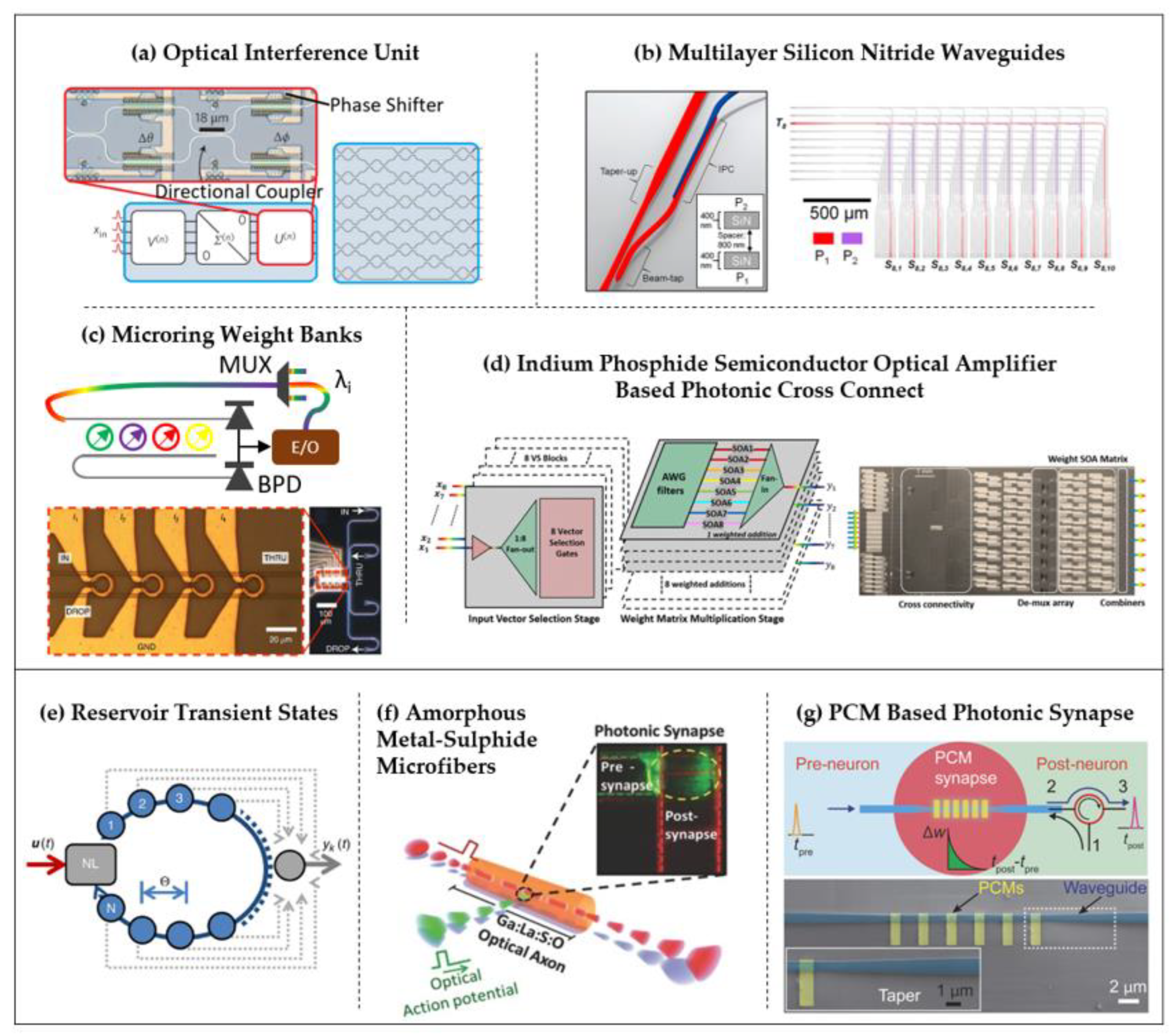
Figure 3.
Integrated photonic neuron with weighting and activation. All-optical: (a) Inputs to SOA-based spiking integrate-and-fire neurons are weighted passively using attenuators and delay lines, temporally integrated with an SOA, and subjected to thresholding using a highly germanium-doped fiber[78]. (b) In a PCM-based spiking neuron, input spikes are weighted using PCM cells and aggregated using a WDM multiplexer (MUX). When the integrated power of the post-synaptic spikes exceeds a threshold, the PCM cell on the ring resonator switches to produce an output pulse [44]. Optical-Electro-Optical: (c) A superconducting optoelectronic spiking neuron employs a superconducting-nanowire single-photon detector (SNSPD) to drive a superconducting switch (amplifier)[79], which is then followed by a silicon light-emitting diode (LED)[80]. (d) Interference neurons based on Mach-Zehnder interferometers (MZI) achieve optical-to-optical activation by converting a fraction of the optical input to implement positive (excitatory) and negative (inhibitory) weights using a photodetector. The remaining original optical signal is intensity-modulated due to the intrinsic nonlinearity of the photodetector[81]. (e) Wavelength division multiplexing (WDM) inputs are weighted using tunable microring resonators (MMRs, Figure 2c). The optical power is aggregated and sensed by a balanced photodiode, which then drives the electro-absorption modulator (EAM) incorporating an indium tin oxide (ITO) layer monolithically integrated into silicon photonic waveguides. This EAM nonlinearly modulates the laser power[82]. (f) The device utilizes WDM to achieve multichannel fan-in and a photodetector to aggregate signals to drive a laser perceptron[83]. In figures e-g, device schematics are depicted on the left, alongside micrographs of each device. Figures adapted with permission from ref.[80], AIP (c) and ref.[82], APL (e). Figures reproduced with permission from ref.[78], OPG (a); ref.[44], SNL (b); ref.[81], IEEE (d); ref.[84], APS (f) and ref.[83], AIP (g).
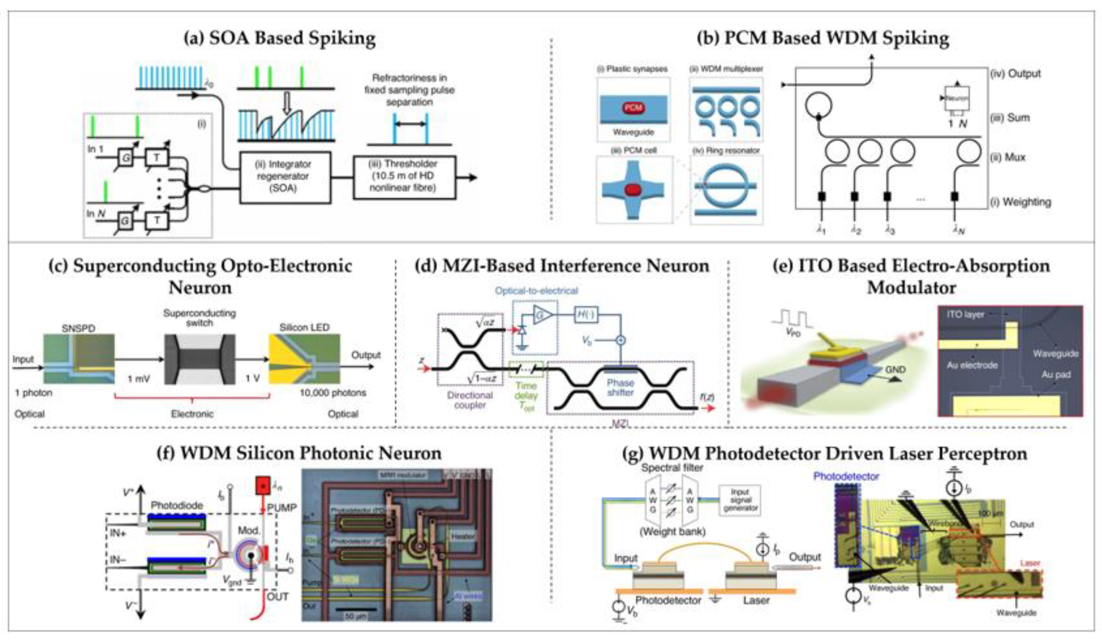
Figure 4.
Spiking photonic neurons. All optical: (a) A semiconductor ring laser featuring an electrically pumped Group III–V MRR coupled to a waveguide (top)[86]. Bistability arises from excitable behavior (bottom)[87] when the symmetry of the two counter-propagating (clockwise or anticlockwise) modes per frequency is disrupted [88]. (b) On the left, an InP-based two-dimensional photonic crystal features an L3 cavity (three holes removed, incorporating quantum wells) that leverages fast third-order nonlinearity to achieve excitability. On the right, hysteresis cycles demonstrate bistability with varying detuning values relative to the cavity resonance, displayed in arbitrary units[89]. (c) A graphene-saturable absorber (SA) is positioned between two fiber connectors. An erbium-doped fiber serves as a gain medium, which is optically injected and pumped[90]. (d) On the left is an optically pumped group III–V micropillar laser with a SA. The amplitude response to a single pulse perturbation versus perturbation energy is depicted for bias pump power relative to the self-pulsing threshold on the right. This illustrates the differentiation between the excitable and self-pulsing thresholds [91]. Optical-Electro-Optical: (e) A two-section gain-SA setup on the left, functioning as an integrate-and-fire mechanism. At the bottom is a micrograph of an electrically injected excitable distributed feedback laser used to selectively disturb the gain, driven by a balanced photodetector pair. On the right, the measured excitable power of the input pulses is displayed at the top, while the laser output is at the bottom [92]. (f) On the left is a resonant-tunneling diode layer stack, photodetector, and laser diode (RTD-LD), constituting an excitable optoelectronic device. On the right, excitability is attained by biasing a double-barrier quantum well within the RTD in the negative differential resistance region of its direct current–voltage curve [93]. Figures adapted with permission from ref.[86], Elsevier (a, bottom) and ref.[94], IEEE (e). Figures reproduced with permission from ref.[87], APS (a, top); ref.[89], APS (b); ref.[90], SNL (c); ref.[91], APS (d) and ref.[93], OPG (f).
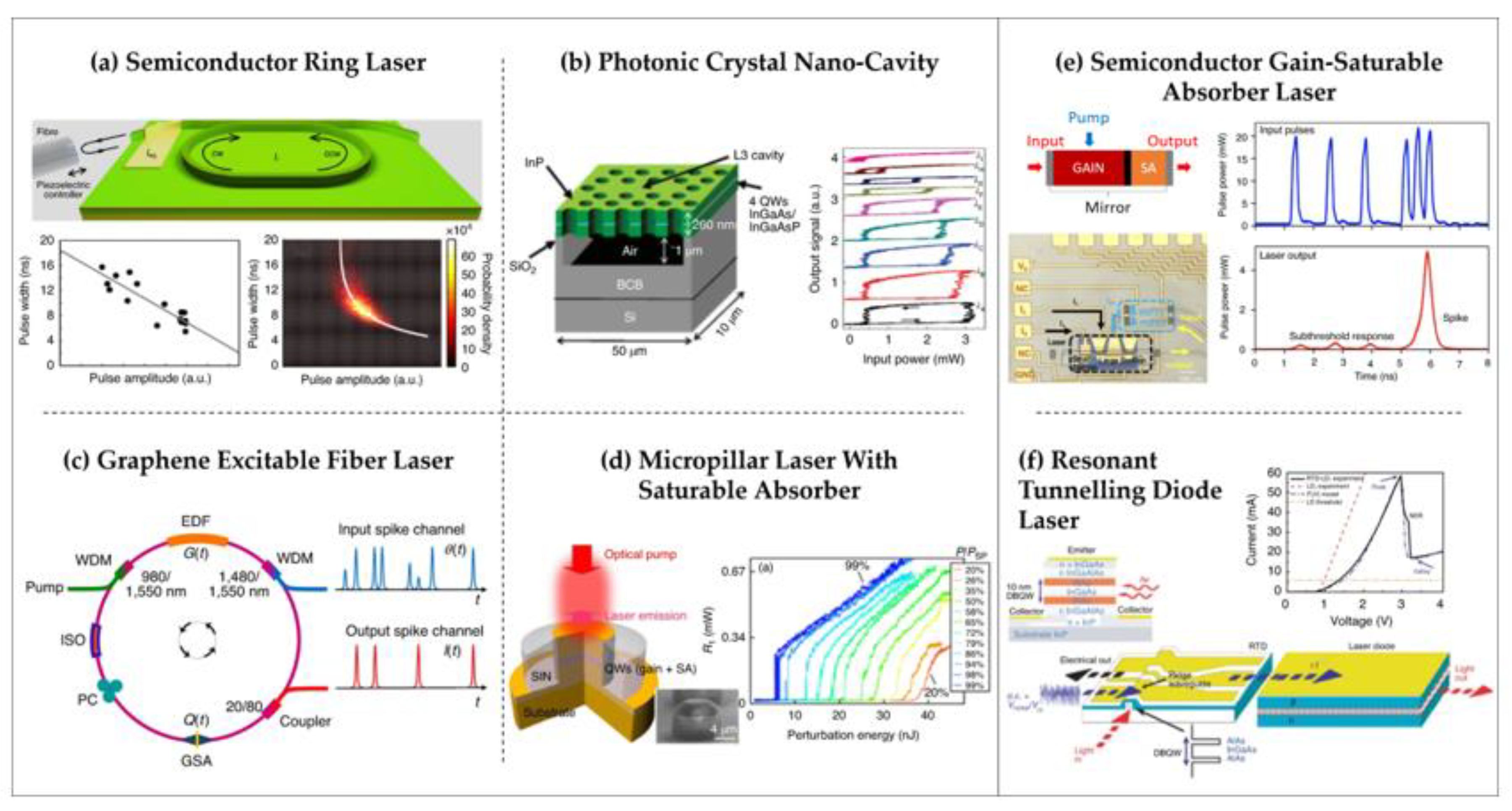
Figure 5.
Artificial intelligence topologies also applicable to neuromorphic photonic networks (NPNs) represented through rectangular Venn diagram. The NPN architecture integrates recurrent and feedforward connections, facilitating advanced learning processes. Dashed lines indicate the lack of direct feedback connections in the feedforward case, while the complete network for the recurrent case elucidates the network's operational dynamics.
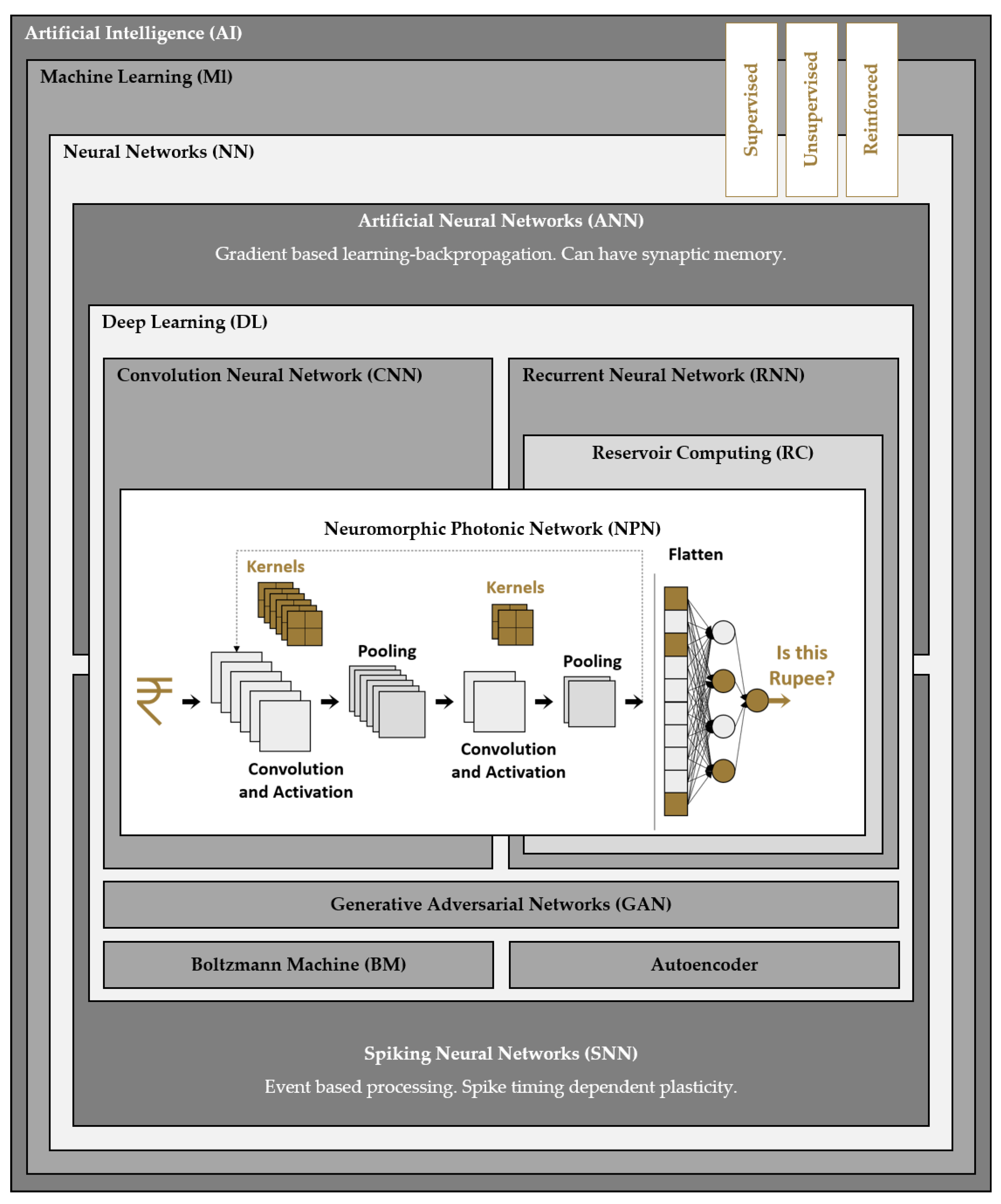
Figure 6.
On-chip neuromorphic photonic approaches. (a) Passive Photonic Reservoir Computing (RC) is a time-delayed recurrent neural network that uses fixed high-dimensional reservoirs for computational tasks depicting input, output, and flow via black and blue arrows and red dots, respectively[61]. (b) A Superconducting Optoelectronic Network (SON) is a feedforward multilayer perceptron using semiconducting few-photon light-emitting diodes and superconducting-nanowire single-photon detectors with N0 neurons[111]. (c) The MZI-based Coherent Nanophotonic Circuit (CNC) is an internally and externally trained feedforward network using phase shifters depicting the optical interference unit that implements matrix multiplication and attenuation via red and blue meshes, respectively[62]. (d) Wavelength division multiplexed Broadcast and Weight Network (B&W) is a recurrent, continuous-time model programmed by a compiler composed of a microring weight bank, a balanced photodiode for summing, and a microring modulator for nonlinear activation[102]. (e) Multiwavelength PCM-based Photonic Neurosynaptic Network (MN) presents a feedforward, spiking model with both external and local training composed of layers, including a collector made up of micro rings that utilize wavelength division multiplexer to unite optical signal from the previous layer (bottom) and a distributor that broadcast signal equally germanium-antimony-tellurium synapse (top)[44]. (f) A feedforward pre-trained on-chip Diffractive Optics Neural Network (DO) with continuous output based on a phase-tunable complex-valued transmission coefficient made up of a silicon slot filled with silicon dioxide (SSSD)[107]. Figures reproduced with permission from ref.[61], SNL (a); ref.[111], APS (b); ref.[62], SNL (c); ref.[84], APS (d); ref.[44], SNL (e) and ref.[107], SNL (f).
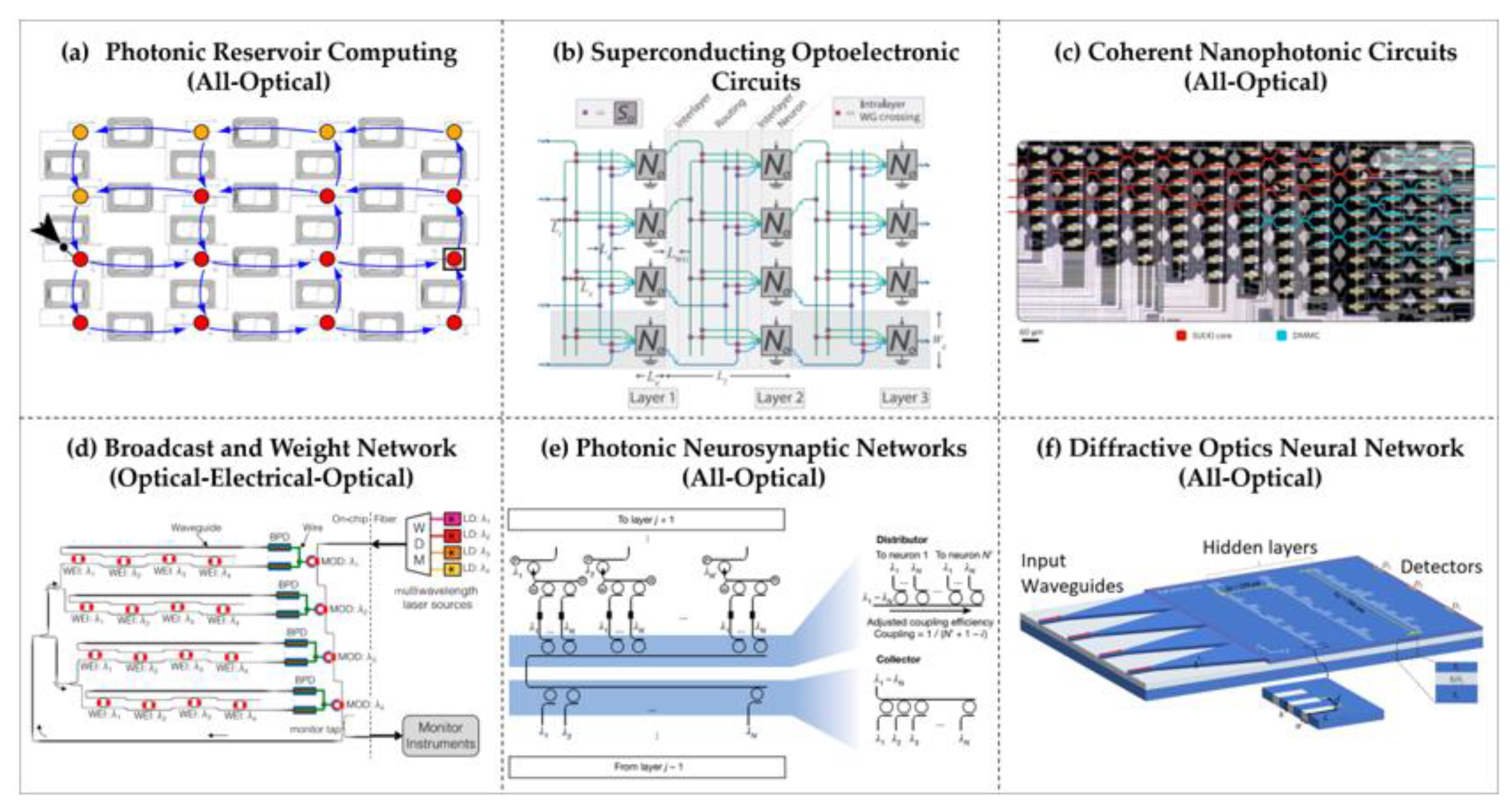
Figure 7.
Applications as a prospect for neuromorphic photonic networks [10].
Figure 7.
Applications as a prospect for neuromorphic photonic networks [10].
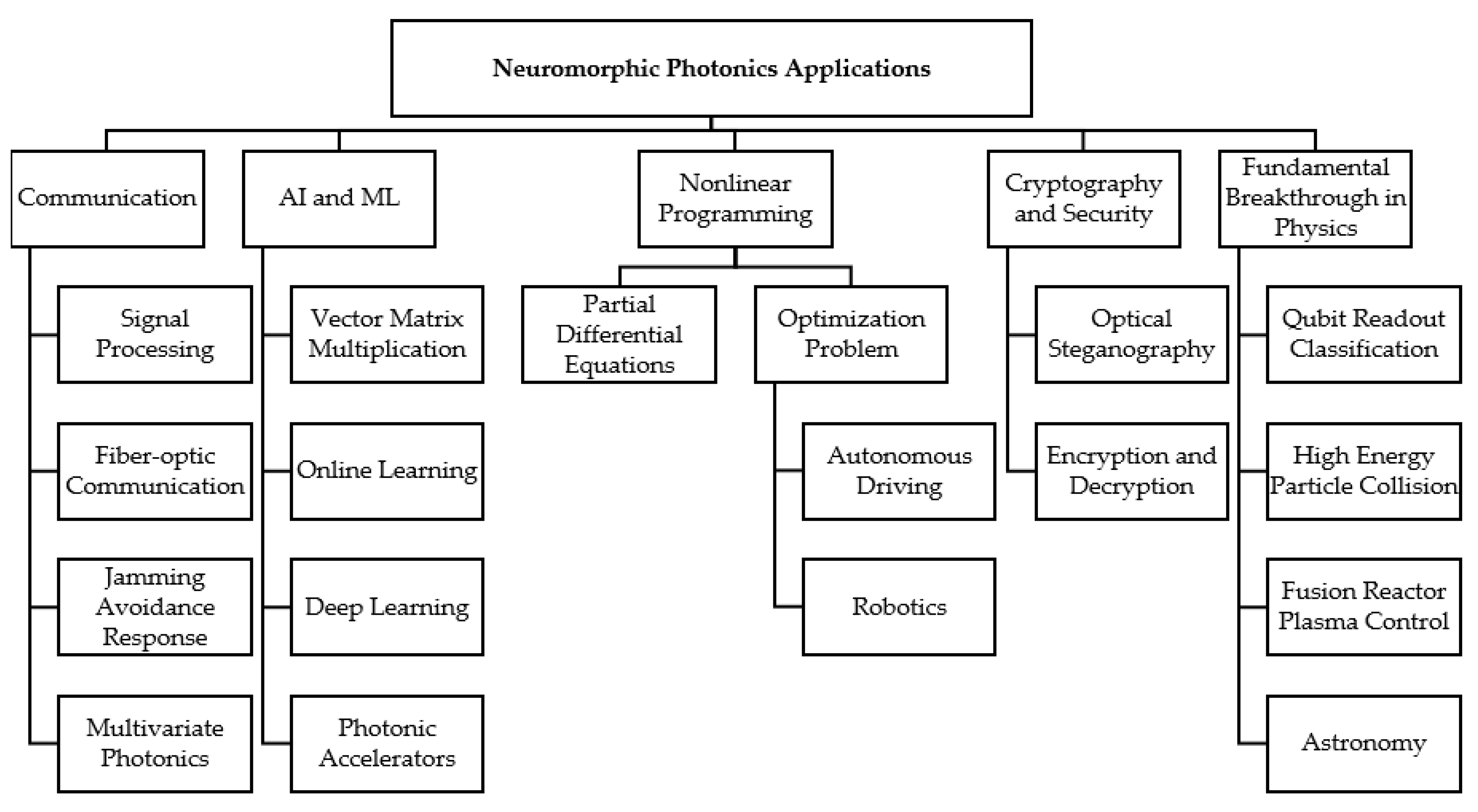

Table 1.
Proposed on-chip approaches for neuromorphic photonic networks.
| NPN Type [Ref.] | Synapse | Synaptic Memory | Photonic Neuron | Physics | Topology | Remarks |
|---|---|---|---|---|---|---|
| RC[61] | Node of reservoir with multiple feedback loops. | 280 ps interconnection delay. | Intrinsic nonlinearity of photodetector. | Superposition Principal. | Reservoir |
No power consumption in the reservoir and high bitrate scalability (> 100 Gbit/sec). Cannot be generalized for complex computing application. |
| SOC[111] | Interplanar or lateral waveguide coupler with electromechanically tunable coupling. | MEMS capacitor. | Phase change nanowires from superconducting to normal metal above a threshold induced by photon absorption arranged in parallel or series detector. | Superconductivity and MEMS capacitance. | ANN and SNN |
Highly scalable, zero static power dissipation, extraordinary device efficiencies. Require cryogenic temperature (2K). Bandwidth limited to 1 GHz. |
| CNC[62] | OIU consisting of beamsplitters and phase shifters for unitary transformation and attenuators for diagonal matrix. | NA | Nonlinear mathematical saturable absorber function. | TO-effect. | Two-layer DNN |
Can implement any arbitrary ANN. May allow online training. Bulky and require high driving voltage. |
| B&W[102] | Reconfigurable TO-MRR filters. | NA | Mach-Zehnder Modulator. | TO-effect. | CTRNN |
Capable of implementing generalized reconfigurable RNN. Bandwidth limited to 1 GHz. |
| MN[44] | Optical waveguides integrated PCM on top, controlling propagating optical mode. | GST dynamics. | Optical ReLU designed via MRR-PCM on top. | WDM and PCM dynamic. | ANN |
No waveguide crossings, no accumulation of errors and signal contamination. PCM cell in endurance support up to 10 switching cycles. |
| DO[107] | Pre trained phase values on distinct hidden layers via SSSD. | NA | Diffractive unit composed of three identical SSSD. | Huygens-Fresnel Principle and TO-effect. | Three-layer DNN |
Scalable, simple structure design and all optical passive operation. Requiring external algorithmic compensation. |
* Micro-electromechanical system (MEMS); Optical Interference Unit (OUI); Thermo-optic (TO); Continuous Time RNN (CTRNN); Silicon slot filled with silicon dioxide (SSSD); Not Applicable (NA); Selected publications based on novelty or experimental demonstration.
Table 2.
Applied training and comparison of on-chip neuromorphic photonic networks.
| NPN Type | Device Basic Unit [Reference] |
Networks and Training | Comparison | ||||||
|---|---|---|---|---|---|---|---|---|---|
| Topology | Training | Data (Train: Test)% |
Application | Remark or Accuracy Exp. (Sim.) |
NBUs/mm2 | Operational Power (pJ/FLOP) | Throughput (TOPS) | ||
| RC | Spiral Nodes[61] | Reservoir | Fivefold cross validation, ridge regression and winner takes all approach. |
10000 bits for Boolean task and 5-bit headers |
Arbitrary Boolean logic and 5-bit header recognition | >99 (-) | 62500 | 0 | 0.4 |
|
SOC |
SNSPD[111] | ANN And SNN |
Backpropagation and STDP | - | - | Designed for Scalability | 7 to 4000 | 0.00014 | 19.6 |
| CNC | Tuneable MZI[62] | Two-layer DNN |
SGD | 360 data points (50:50) | Vowel recognition |
76.7 (91.7) |
<10 | 0.07600 | 6.4 |
| B&W | TO-MMR[102] | CTRNN | Bifurcation Analysis | 500 data point from 0.05 to 0.85 | Lorenz attractor | B&W is Isomorphic to CTRNN | 1600 | 288.0000 | 1.2 |
| MN | MRR-PCM[44] | ANN | Backpropagation STDP | Four 15-pixel images, A-D | Pattern Recognition | Recognized letters | - | - | - |
| X-PCM[105] | CNN | Backpropagation | MNIST handwritten digits | Digit Recognition | 95.3 (96.1) | <5 | 0.00590 | 28.8 | |
| DO## | SWU [107] | Three-layer DNN |
Pretrained backpropagation (adaptive moment estimation) | Iris (80:20) and MNIST handwritten digits (85:15) |
Classification | 90 (90) and 86 (96.3) |
2000 | 0.00001 | 13800.0 |
| ‡ For more comprehensive information readers may also refer to other reported works [27,96,97,104,117,118,123,124,125]. | |||||||||
# No of basic unit (NBU); Trillions of operations per second (TOPS) = 2*No. of layers in network*No. of rows*No. of columns*Detection rate; Floating point operations (FLOPS); X represent ring or MAC unit; Sub wavelength unit (SWU); ## Reported 30% Fabrication Error; Selected publications based on novelty or experimental demonstration.
Disclaimer/Publisher’s Note: The statements, opinions and data contained in all publications are solely those of the individual author(s) and contributor(s) and not of MDPI and/or the editor(s). MDPI and/or the editor(s) disclaim responsibility for any injury to people or property resulting from any ideas, methods, instructions or products referred to in the content. |
© 2024 by the authors. Licensee MDPI, Basel, Switzerland. This article is an open access article distributed under the terms and conditions of the Creative Commons Attribution (CC BY) license (http://creativecommons.org/licenses/by/4.0/).
Copyright: This open access article is published under a Creative Commons CC BY 4.0 license, which permit the free download, distribution, and reuse, provided that the author and preprint are cited in any reuse.


