Submitted:
25 July 2024
Posted:
26 July 2024
You are already at the latest version
Abstract
This Paper delves into a thorough analysis of the DC-DC buck converter tailored for renewable energy applications. Given the prevalent utilization of renewable resources producing DC voltages, this converter plays a pivotal role in stepping down high-level DC voltages to more manageable levels. The research focuses on varying the duty cycle to assess its impact on the converter's output voltage performance. Simulations conducted using PSIM are meticulously compared with hardware implementation results, demonstrating the converter's efficacy in generating significantly reduced output voltages. The findings underscore the practical applicability of this converter in renewable energy scenarios, offering a succinct yet insightful perspective on its performance and adaptability.
Keywords:
DC
; Buck converter
; energy
; simulations
1. Introduction
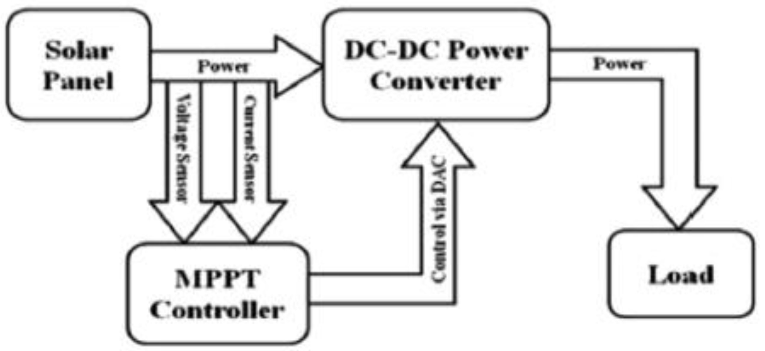
Given the prevalence of DC voltage in most renewable energy sources, DC-DC converters play a crucial role in adjusting voltage levels for various applications [1]. These converters, now integral to modern electronic systems, find extensive use in photovoltaic (PV) applications for maximum power point tracking (MPPT) [1,2]. Different converter types, such as buck, boost, buck-boost, cuk, sepic, and zeta, are employed in PV applications to track peak power efficiently [1,2]. The buck converter consistently produces an output voltage lower than its input, while the boost converter yields an output voltage higher than the input [3]. The buck-boost converter, influenced by its duty cycle (D), can generate an output either higher or lower than the input voltage [3]. By adjusting the duty cycle, load matching is achieved in PV applications, ensuring the efficient transfer of maximum power from the PV panel to the load [4].
Figure 1.
PV system with DC-DC converter and MPPT [4].
Figure 1.
PV system with DC-DC converter and MPPT [4].
2. Configuration of DC-DC Buck Converter
The fundamental structure of a DC-DC buck converter encompasses power switches, such as MOSFET or BJT, serving as pivotal controllers for pulses. Illustrated in Figure 2, this circuit employs MOSFET as the power switch, facilitating the reduction of high-level DC voltage to a lower level. The resulting output voltage consistently remains less than the input voltage [1]. The primary objective of this circuit is to generate a pure DC output, prompting the incorporation of a filter, such as the LC low pass filter, into the basic configuration. During the ON state of the switch, the diode assumes a reverse bias, supplying energy to both the load and the inductor. Conversely, in the OFF state, the diode switches to a forward bias, allowing the flow of inductor current through it, transferring stored energy to the load. This versatile circuit configuration accommodates connection to low loads from high-level voltages [3] and finds applicability in high-range step-down converters [6].
3. Mathematical Analysis of DC-DC Buck Converter
In this section, we delve into examining the interplay between the input voltage (Vs) and the duty cycle in the context of generating a lower output voltage, focusing on the dynamics of the buck converter. The output voltage (Vo) is contingent upon the duty cycle, and Equation (1) serves as a tool for calculating the output voltage based on this parameter. Additionally, during the design phase of the buck converter, Equations (2) and (3) come into play for determining the inductor value. To ensure continuous circuit operation, the calculated inductor value must surpass the minimum value () by 25%, as indicated by Equation (2). The determination of both the maximum inductor current () and minimum inductor current () is facilitated by Equations (4), (5), and (6). Notably, must maintain a positive value to sustain continuous current. Moreover, the capacitor value (C) can be ascertained through Equation (7), incorporating the output ripple voltage as a fraction of the output voltage. This comprehensive analysis establishes a robust understanding of the intricate relationships governing the buck converter's performance.
4. Methodology
The DC-DC buck converter is meticulously devised to efficiently reduce a 5 VDC voltage source to distinct output levels of 2 V and 3 VDC. The chosen switching frequency, set at 25 kHz, surpasses the 20 kHz threshold to preempt audio noise interference, considering a load resistance (R) of 10 ohms and a 10uF capacitor (C). Extensive testing is conducted with duty cycle variations of 0.4 and 0.6, aimed at generating 2 V and 3 VDC voltages, respectively. Employing PSIM software, the circuit simulation integrates calculated parameters derived from Equations (1) to (7), and subsequent analysis is performed on the output waveforms. To refine the output into a purely DC voltage, a low-pass filter is incorporated into the circuit.
The hardware implementation necessitates a meticulous component selection process, contingent on the maximum current and voltage tolerance stipulated in their specifications. This includes judicious consideration of MOSFET and diode capacity to withstand current and voltage stress during both on and off conditions. Additionally, the inductor's ability to sustain maximum current and operate at a specified frequency is taken into account to avert component breakdown.
The designed hardware undergoes rigorous testing, analysis, and measurement, employing tools such as oscilloscopes and digital multimeters. Manipulating the duty cycle between 0.4 and 0.6 yields the anticipated 2 V and 3 VDC voltages. The MOSFET, driven by a gate driver, plays a pivotal role in toggling the pulses on and off. Consistency in parameters—inductor (150uH), capacitor (10uF), and resistor (10Ω)—is maintained across both simulation and hardware testing phases, ensuring a comprehensive evaluation of the buck converter's performance.
5. Analysis of Simulated Results and Hardware Implementation
A comprehensive examination of the DC buck converter involves scrutinizing both the simulated results and its practical hardware implementation, facilitating a thorough understanding of the converter's performance. The amassed data is meticulously recorded and tabulated, setting the stage for an in-depth discussion.
5.1. Simulation Results
The circuit design for the DC-DC buck converter, adept at transforming high input DC voltage into a lower output, is visually depicted in Figure 3. Executed within the PSIM environment, the simulation offers insightful results. Voltmeters, specifically labeled Vind," Vdiode, Vcap and Vout play a pivotal role in gauging the voltage drop across key components—the inductor, diode, capacitor, and load resistor, respectively. These recorded measurements serve as essential metrics for evaluating the simulated performance, paving the way for a nuanced analysis of the converter's behavior under varying conditions. The subsequent discourse will delve into the implications of these results and their alignment with theoretical expectations.
Figure 4 illustrates the output waveform under a duty cycle of 0.4, while Figure 5 captures the corresponding waveform under a duty cycle of 0.6. Notably, the output voltage waveform aligns with 2 V for the 0.4 duty cycle and 3 V for the 0.6 duty cycle. This distinct variation in output voltages based on duty cycle nuances is critical for understanding the converter's behavior. The recorded comparative data, meticulously documented in Table 1 for both duty cycles, serves as a comprehensive reference for further analysis. The symbiotic relationship between the duty cycle and output voltage becomes apparent in the simulation results, indicating a proportional correlation. Specifically, as the duty cycle diminishes, the output voltage proportionally decreases, underscoring the dynamic influence of the duty cycle on the converter's output. This nuanced exploration elucidates the intricacies of the converter's response to varying duty cycle parameters, contributing to a deeper comprehension of its operational characteristics.
5.2. Analysis of Hardware Prototype Results
The examination of the hardware prototype involves an intricate analysis of output waveforms, voltage readings across components, and the current flow through these components. These detailed measurements serve as essential data points for a comprehensive evaluation of the hardware implementation, enriching the understanding of the converter's practical performance.
For an in-depth exploration, the recorded data is meticulously documented for further scrutiny and comparison. As illustrated in Table 1, a notable discrepancy emerges in the output voltage across the load when juxtaposed with the simulation and calculated values. This discrepancy can be attributed to inherent losses stemming from elevated voltage drops across the diode and harmonic issues within the hardware prototype. To address this concern and enhance efficiency, a proposed solution involves substituting the diode with a second MOSFET characterized by a lower voltage drop, thereby mitigating losses and optimizing performance.
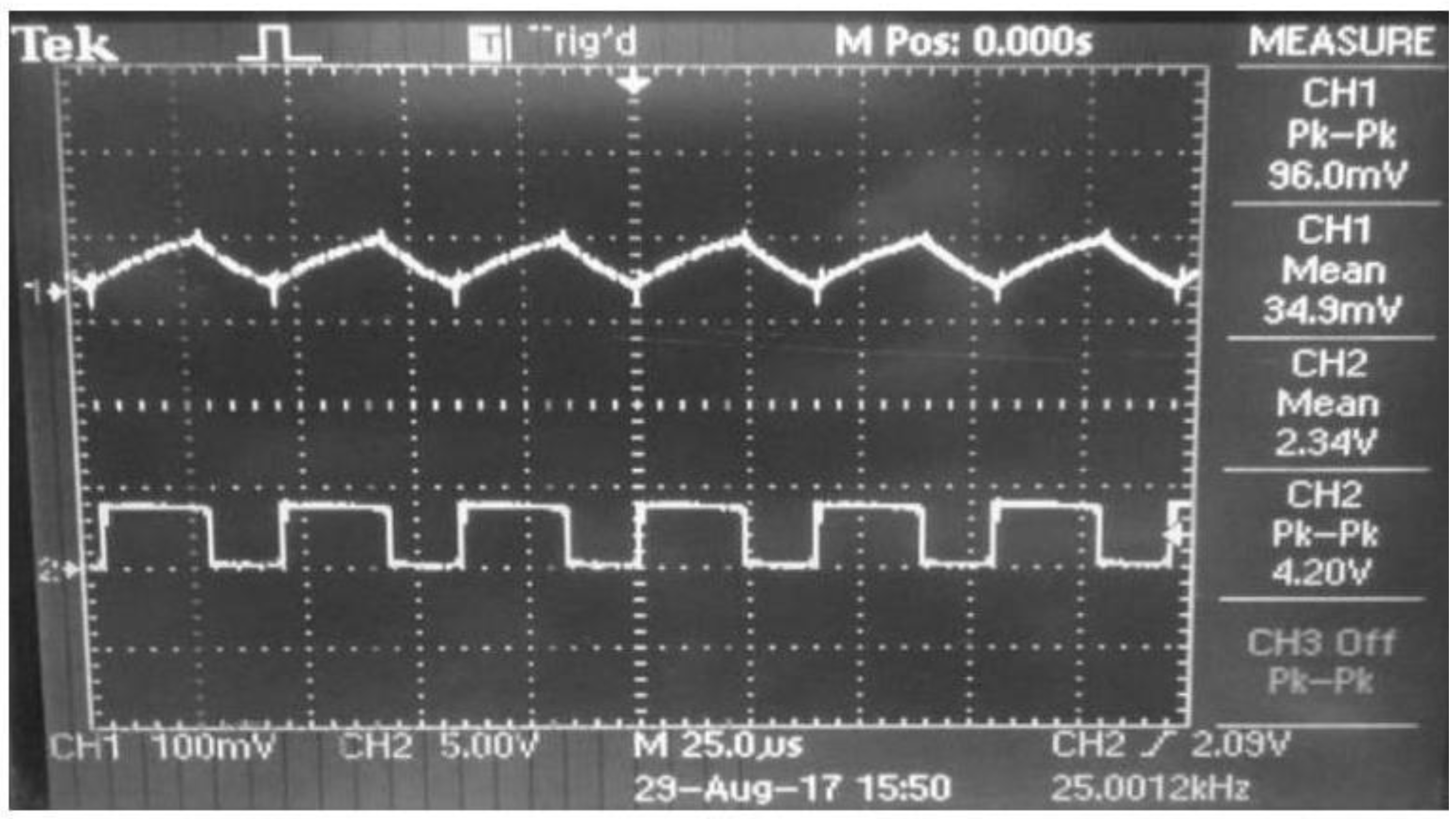
Figure 6, Figure 7, Figure 8, Figure 9 and Figure 10 complement this analysis, presenting the output waveforms across key elements of the DC buck converter, including the capacitor, diode, inductor, load resistor, and the inductor current. This visual representation offers a nuanced insight into the hardware dynamics, aiding in the identification of potential areas for refinement and optimization. The recorded data and corresponding figures lay the foundation for a comprehensive discussion on the practical implications of the hardware prototype, setting the stage for further enhancements and refinements in future iterations.
Figure 6.
a) Load resistor output voltage at (a) duty cycle, D of 0.4 (b) duty cycle, D of 0.6.
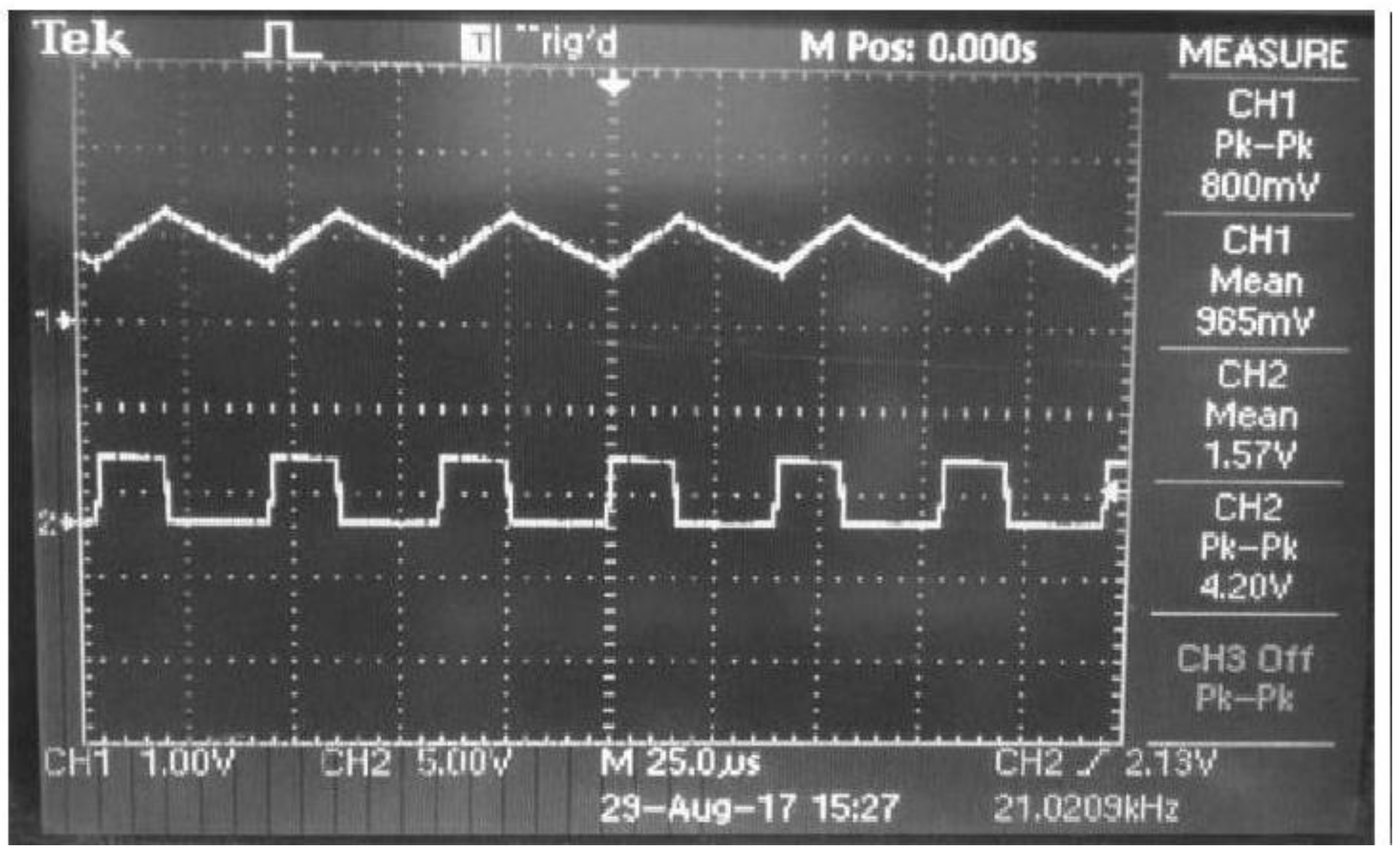
Figure 7.
b) Load resistor output voltage at (a) duty cycle, D of 0.4 (b) duty cycle, D of 0.6 .
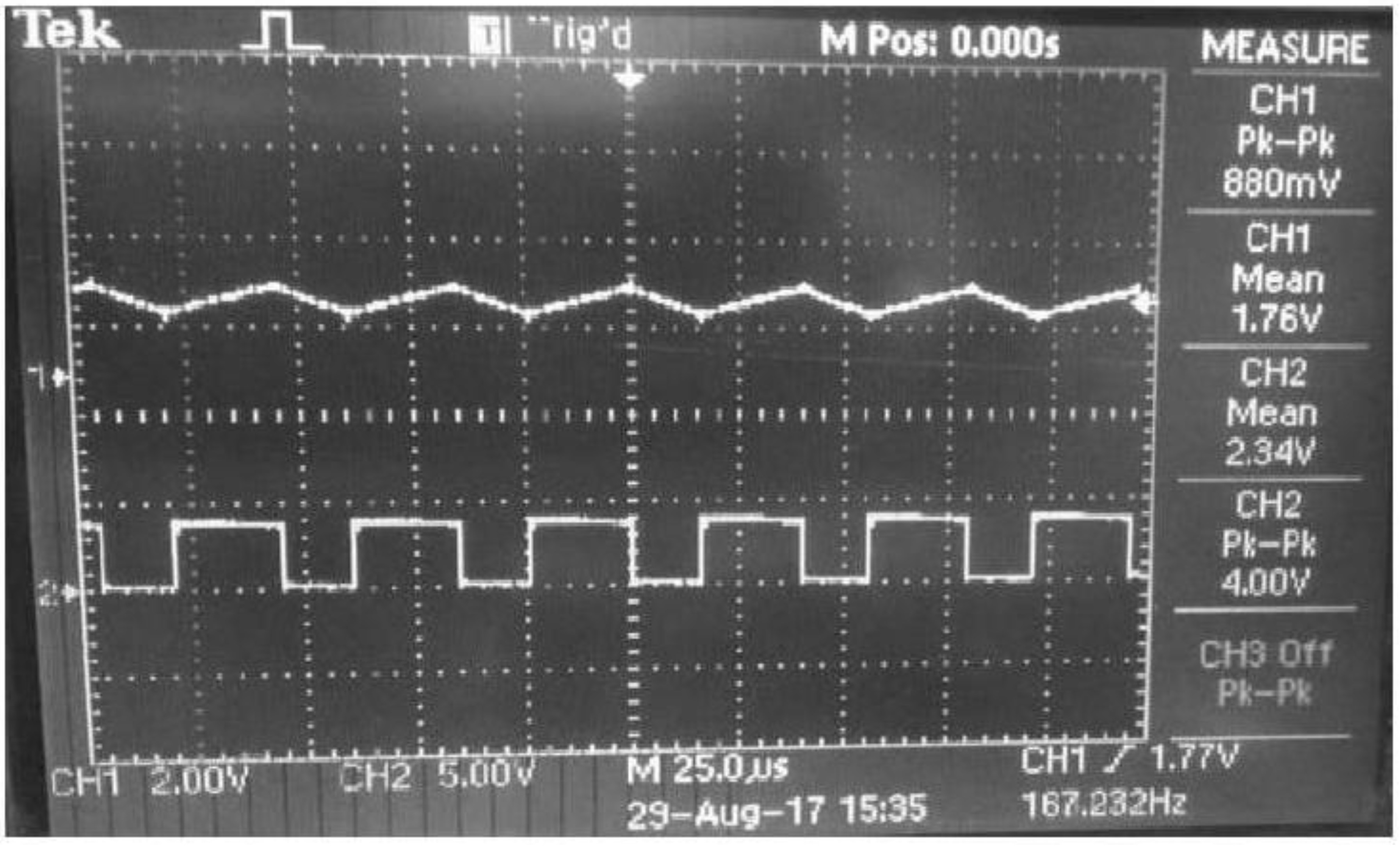
Figure 7.
(a) Diode voltage at (a) duty cycle, D of 0.4 (b) duty cycle, D of 0.6.
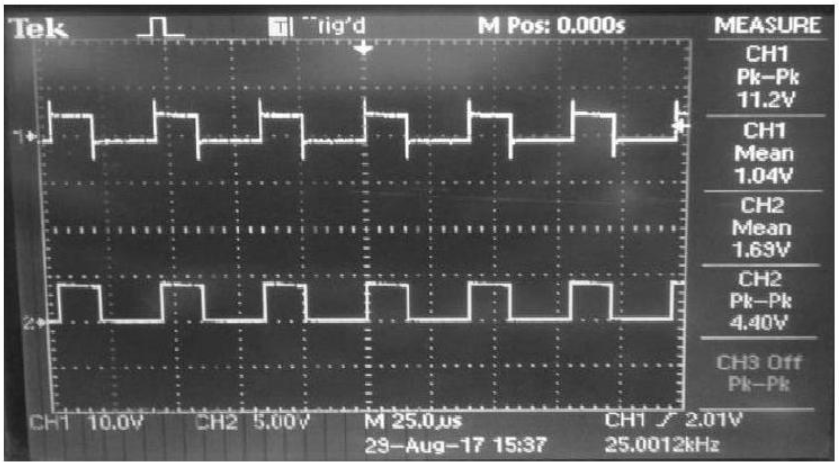
Figure 7.
(b) Diode voltage at (a) duty cycle, D of 0.4 (b) duty cycle, D of 0.6.
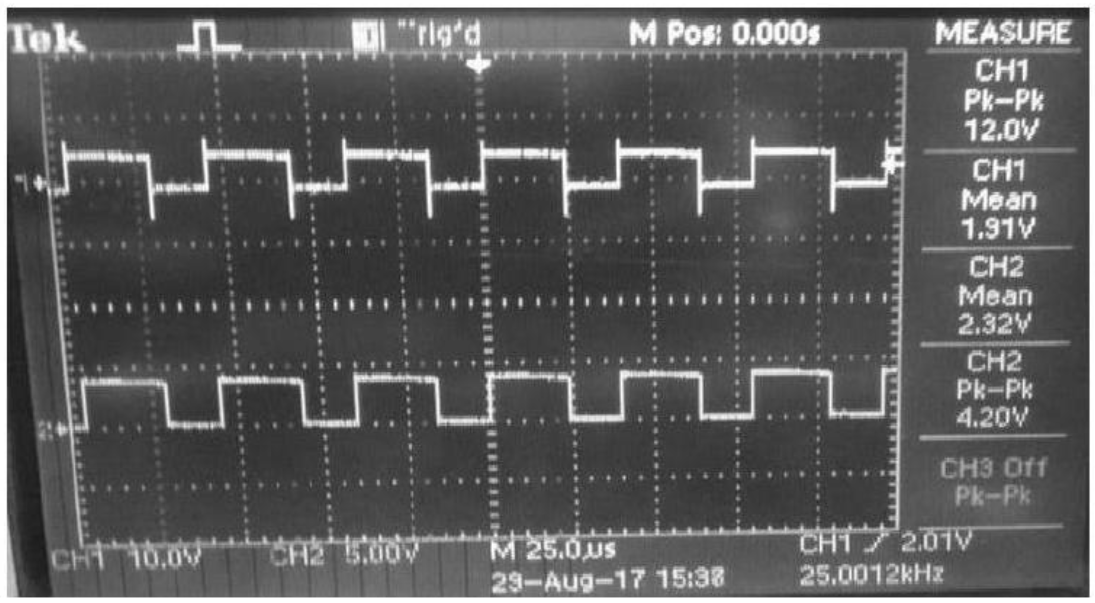
Figure 8.
a) Inductor voltage at (a) duty cycle, D of 0.4 (b) duty cycle, D of 0.6 .
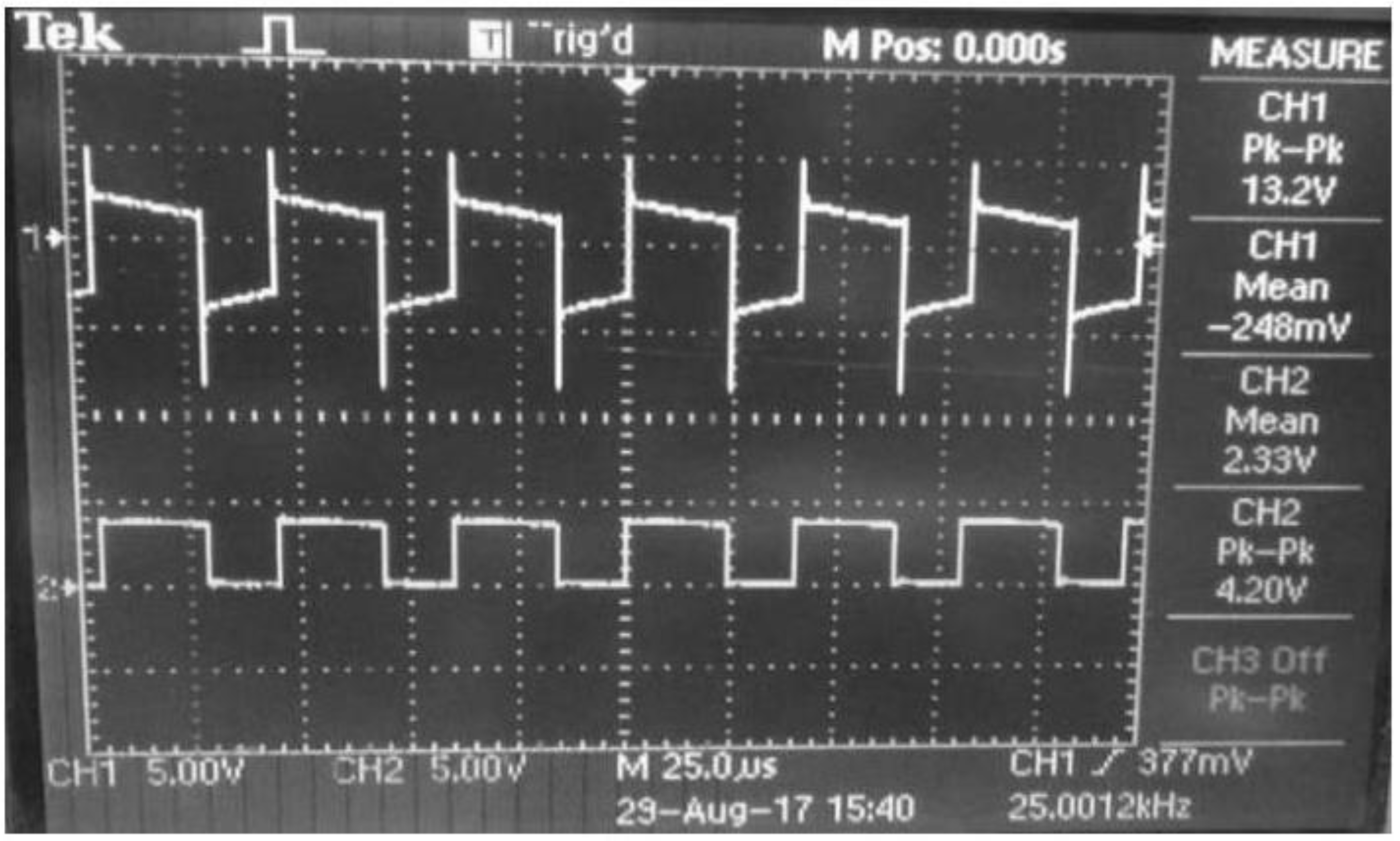
Figure 9.
b) Inductor voltage at (a) duty cycle, D of 0.4 (b) duty cycle, D of 0.6 .

Figure 9.
(a) Capacitor voltage at (a) duty cycle, D of 0.4 (b) duty cycle, D of 0.6.
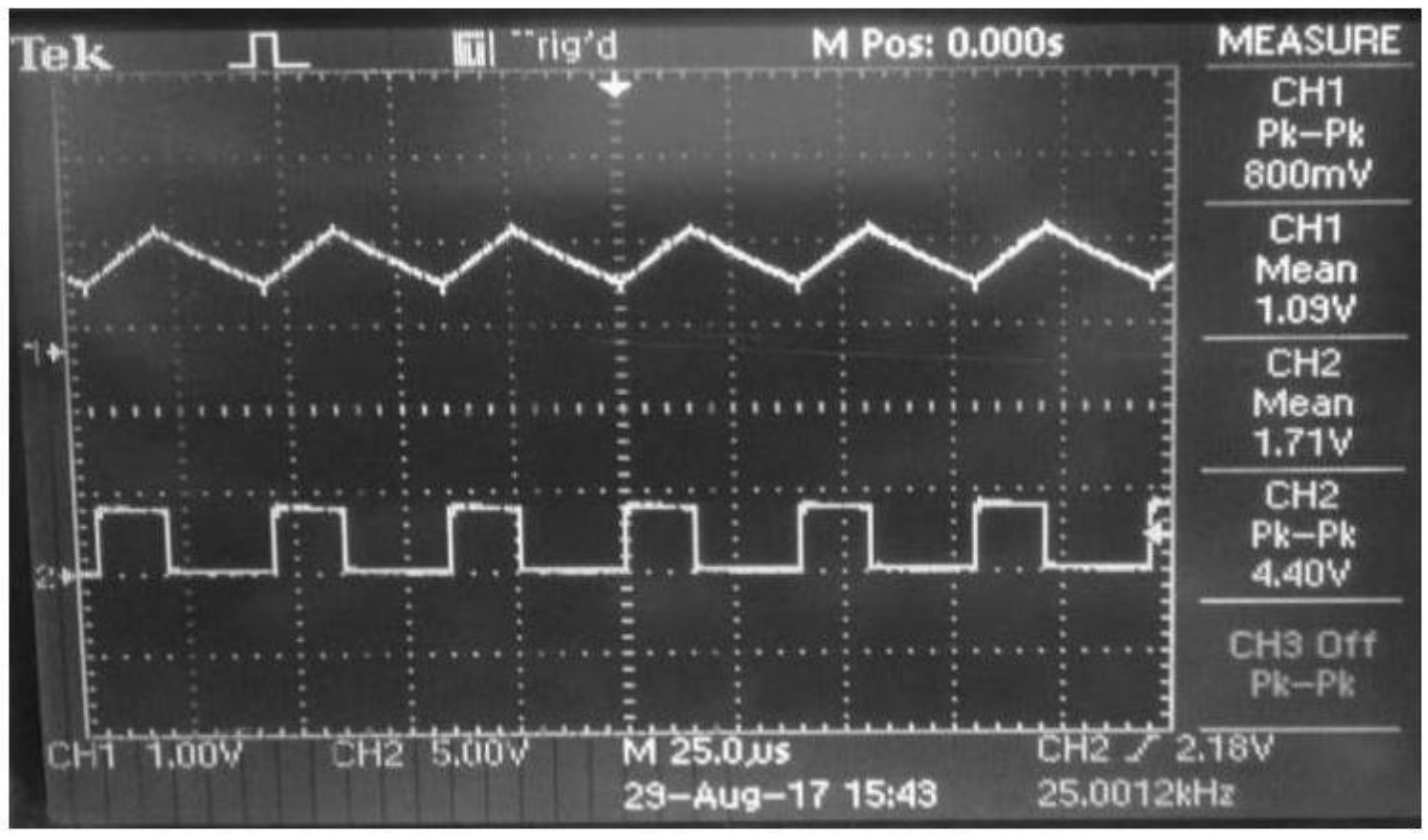
Figure 9.
(b) Capacitor voltage at (a) duty cycle, D of 0.4 (b) duty cycle, D of 0.6.
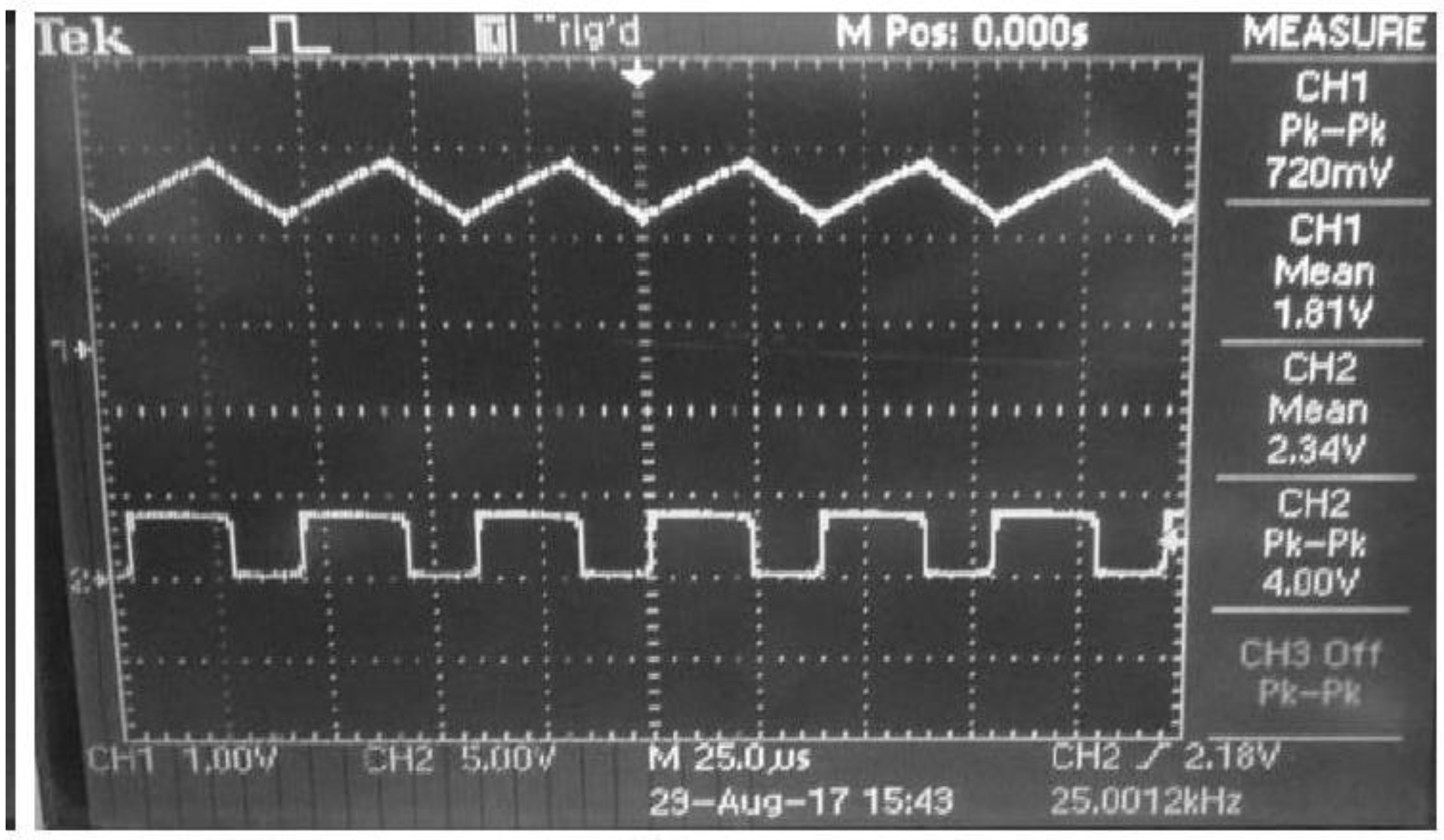
Figure 10.
a) Inductor current (a) duty cycle, D of 0.4 (b) duty cycle, D of 0.6.
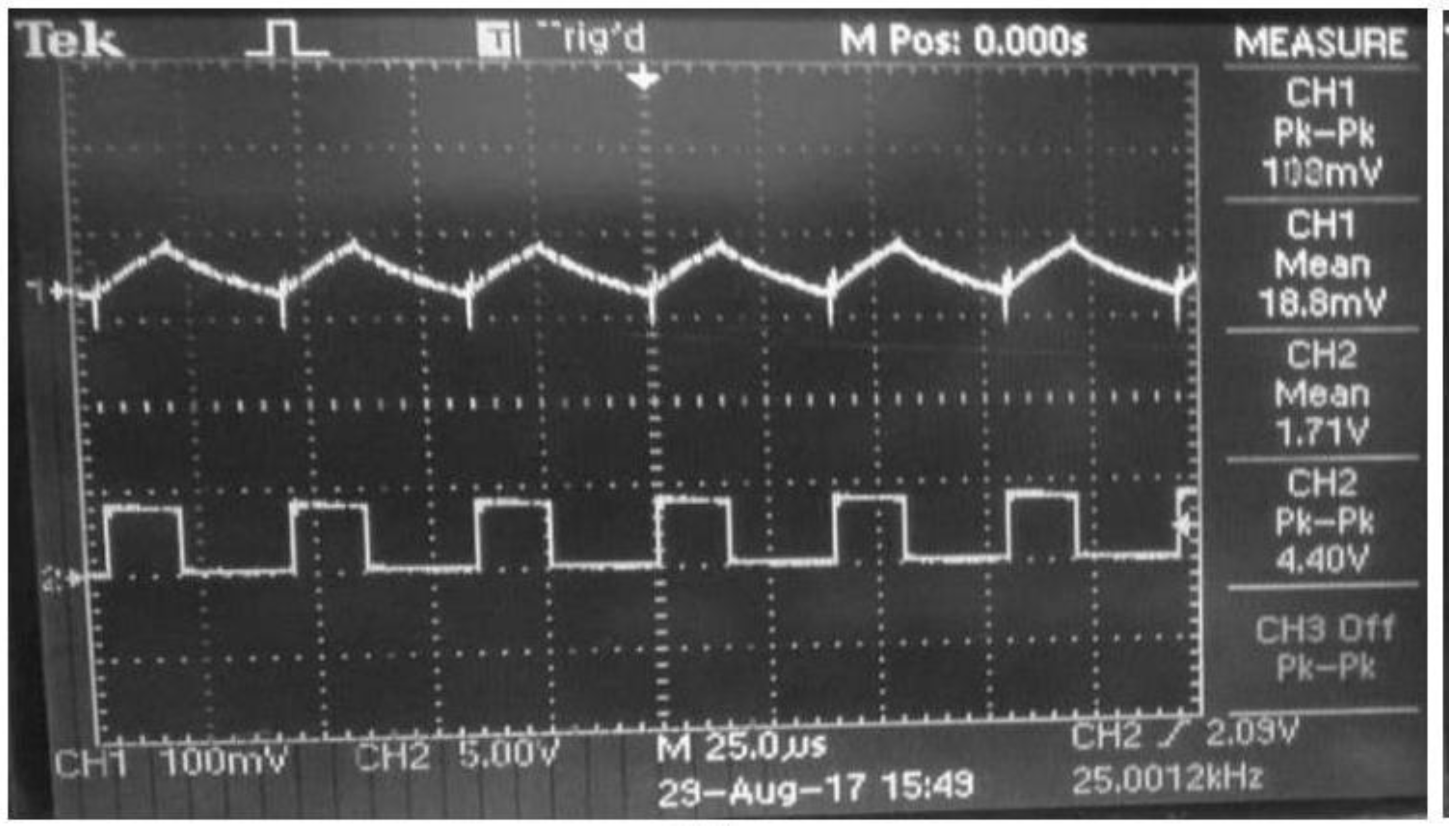
Figure 10.
(b) Inductor current (a) duty cycle, D of 0.4 (b) duty cycle, D of 0.6.
5.3. Comparative Analysis: Simulation vs. Hardware Implementation Results
The juxtaposition of simulation and hardware implementation results entails a meticulous exploration of the designed DC buck converter's performance under varying duty cycles. Table 2 provides an insightful comparison encompassing calculations, simulations, and hardware prototype outcomes for different duty cycles, namely D = 0.4 and D = 0.6. The experiment systematically manipulates the duty cycle to scrutinize its impact on the output voltages.
The recorded data illustrates a noteworthy distinction between the calculated and simulated values in contrast to the hardware prototype results, particularly when the duty cycle is altered. It is observed that the output voltage and current obtained from the hardware prototype are halved compared to the calculated and simulated values. This divergence is attributed to inherent losses incurred during instances of elevated voltage drops across the diode and harmonic issues within the practical hardware setup.
Table 2 encapsulates a summary of the designed DC buck converter's performance parameters under varying duty cycles, shedding light on the nuanced intricacies between theoretical expectations, simulations, and the real-world hardware implementation. This comprehensive comparative analysis lays the groundwork for a deeper understanding of the converter's behavior, providing valuable insights for refining and optimizing its practical performance in future iterations.
6. Concluding Insights: Optimizing DC Buck Converter for Renewable Energy Applications
This paper systematically delves into the analysis of a DC buck converter with applications geared towards the renewable energy sector. The converter, adept at reducing or stepping down input voltages as per load requirements, emerges as a pivotal component in sustainable energy systems. The variable duty cycle of the DC buck converter proves instrumental in tailoring the output voltage proportionally to specific needs, offering adaptability in renewable energy scenarios.
While the hardware implementation unveils a notable reduction in output voltage compared to simulation and calculations, a strategic remedy is proposed. Introducing a second MOSFET in lieu of the diode emerges as a viable solution to mitigate losses and diminish voltage drops. This proposed enhancement aligns with the paper's overarching objective of optimizing the converter's efficiency in practical applications.
In essence, this study not only contributes to the theoretical understanding of DC buck converters in renewable energy applications but also underscores the practical challenges encountered during hardware implementation. The proposed solution serves as a stepping stone for future advancements, emphasizing the dynamic nature of sustainable energy technologies and the continual need for innovation to address real-world complexities.
Funding
Conflicts of Interest
References
- Dileep, G.; Singh, S.N. Selection of non-isolated DC-DC converters for solar photovoltaic system。 Renew. Sustain. Energy Rev. 2017, 76, 1230–1247. [Google Scholar]
- Ali, U.S. Z-source DC-DC Converter with Fuzzy Logic MPPT Control for Photovoltaic Applications. Energy Procedia 2016, 90, 163–170. [Google Scholar] [CrossRef]
- Taghvaee, M.H.; Radzi, M.A.M.; Moosavain, S.M.; Hizam, H.; Marhaban, M.H. A current and future study on non-isolated DC-DC converters for photovoltaic applications. Renew. Sustain. Energy Rev. 2013, 17, 216–227. [Google Scholar] [CrossRef]
- D. G; Singh, S.N. Selection of non-isolated DC-DC converters for solar photovoltaic system. Renew. Sustain. Energy Rev. 2017, 76, 1230–1247. [Google Scholar] [CrossRef]
- Jain, P.K.; Thermal, W.; Station, P.; State, G.; Corporation, E.; Kumar, A. , "Interleaved DC to DC Buck Converter for Low Power Application," pp. 0–4, 2015.
- Ali, M.S.; Kamarudin, S.K.; Masdar, M.S.; Mohamed, A. An Overview of Power Electronics Applications in Fuel Cell Systems : DC and AC Converters. Sci. World J. 2014, 2014, 1–9. [Google Scholar] [CrossRef] [PubMed]
- Hossain, M.K.; Ali, M.H. Transient stability augmentation of PV/DFIG/SG-based hybrid power system by parallel-resonance bridge fault current limiter. Electr. Power Syst. Res. 2016, 130, 89–102. [Google Scholar] [CrossRef]
Figure 2.
Buck converter topology [5].
Figure 2.
Buck converter topology [5].
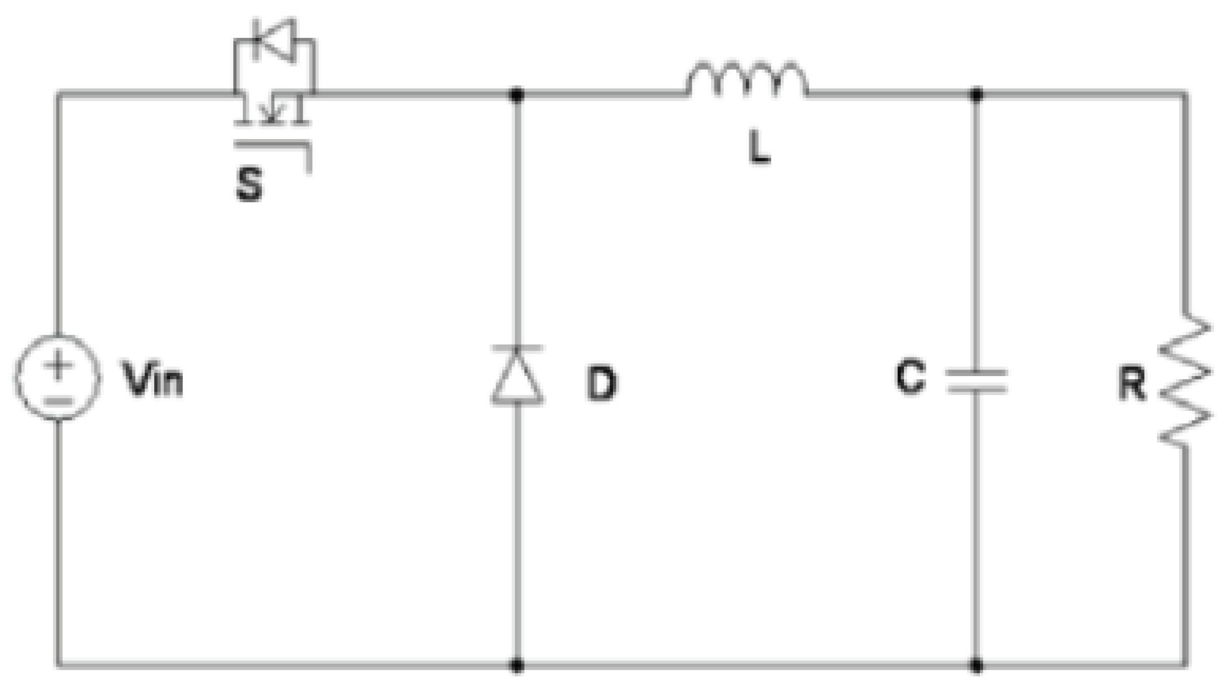
Figure 3.
The designed of DC buck converter.
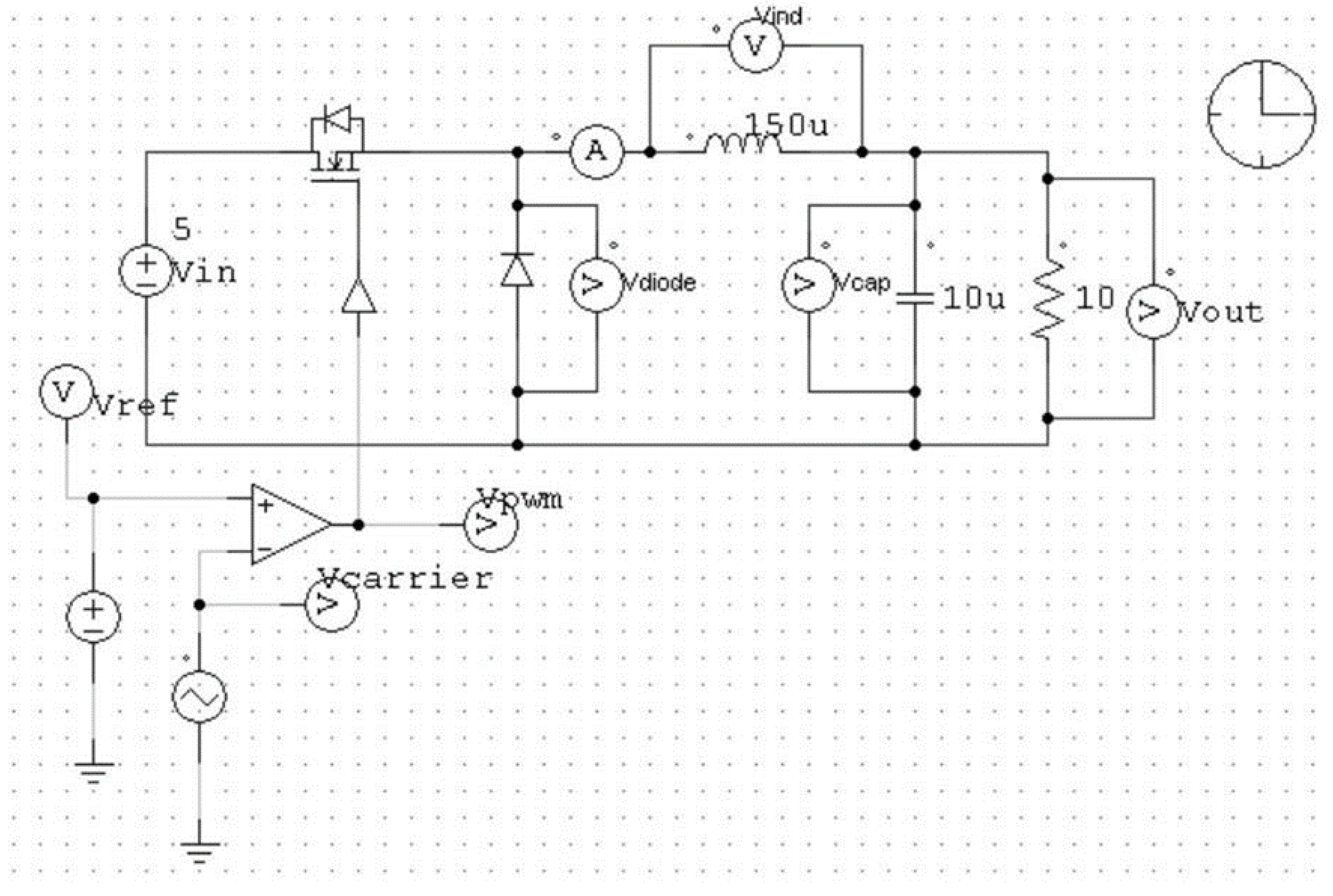
Figure 4.
Output waveforms when the duty cycle is 0.4.
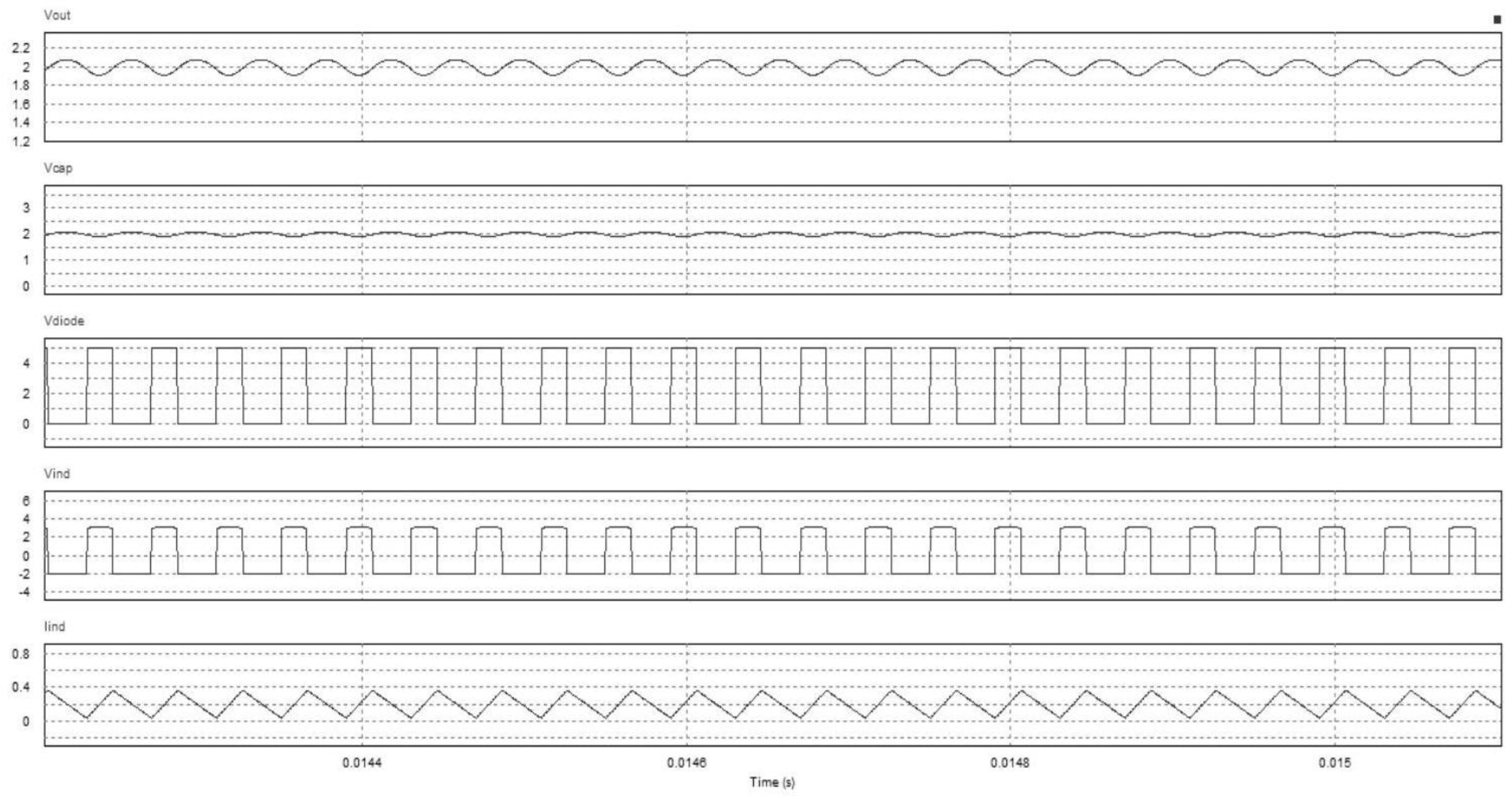
Figure 5.
Output waveforms when the duty cycle is 0.6.
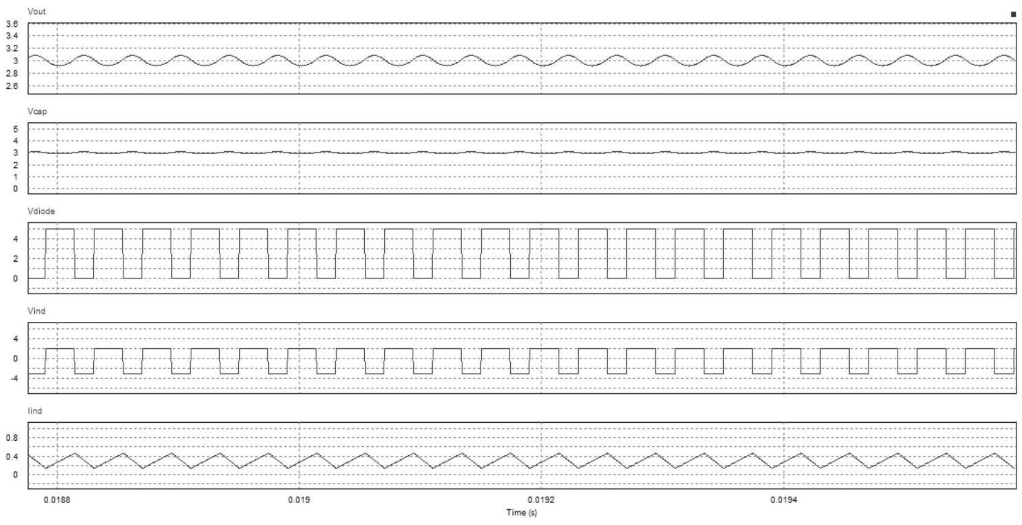

Table 1.
Comparison of hardware results for different duty cycle.
| Parameters | ||
|---|---|---|
Table 2.
Summary results of the designed DC buck converter.
| Parameters | Duty Cycle, D = 0.4 | |||||
|---|---|---|---|---|---|---|
| Calculation | Simulation | Hardware | Calculation | Simulation | Hardware | |
Disclaimer/Publisher’s Note: The statements, opinions and data contained in all publications are solely those of the individual author(s) and contributor(s) and not of MDPI and/or the editor(s). MDPI and/or the editor(s) disclaim responsibility for any injury to people or property resulting from any ideas, methods, instructions or products referred to in the content. |
© 2024 by the author. Licensee MDPI, Basel, Switzerland. This article is an open access article distributed under the terms and conditions of the Creative Commons Attribution (CC BY) license (https://creativecommons.org/licenses/by/4.0/).
Copyright: This open access article is published under a Creative Commons CC BY 4.0 license, which permit the free download, distribution, and reuse, provided that the author and preprint are cited in any reuse.


