Submitted:
31 May 2024
Posted:
31 May 2024
You are already at the latest version
Abstract
Many advanced technologies have been employed in the high performance active matrix displays including liquid crystal displays, organic light emitting diode displays, and micro light emitting diode displays. On the other side, there have existed the strong demand on the cost reduction and it is one of low cost schemes to integrate the driver circuit in a panel based on thin film transistor technologies. This paper reviews overall concept, operation principles, and various circuit approaches in shift registers for the scanning pulse generation. In addition, it deals with the implementation of additional functionalities in gate drivers to support pixel compensation, multi-line driving, in-cell capacitive touch screen, pixel sensing, and adaptive scanning region control.
Keywords:
active matrix display
; gate driver
; shift register
; thin film transistor
; low cost
; scanning pulse generation
1. Introduction
Displays are the visual apparatuses that transfer the visual information to the user by means of images. While liquid crystal displays (LCDs) [1,2,3,4,5,6,7] dominated the display market from smartphones to televisions, organic-light-emitting-diode (OLED) displays [8,9,10,11,12,13] have recently become a mainstream in smartphones and tablet-PCs. Micro-light-emitting-diode (mLED) displays [14,15,16,17,18,19] are getting lots of attention as a future display technology to realize high luminance as well as high reliability in addition to various advantages of self-emissive displays like OLED displays. Also, the application has been extending up to augmented reality/virtual reality/mixed reality (AR/VR/MR) head-mounted displays (HMDs) [20,21,22,23,24,25] and automotive displays [26,27,28,29].
A display consist of numerous pixels that are respectively programmed to control their colors and luminances. Because the number of pixels is millions more, it is impossible to update them with the tremendously large number of dedicated lines. Thus, the matrix driving scheme with column and row lines has been employed to reduce the number of lines to access pixels [30,31,32,33,34,35,36,37,38,39]. Pixels are addressed line by line, where only pixels in a line are programmed at the same time and pixels of other lines are sequentially updated. This line-by-line update operation is called scanning. Usually, column signals carry the pixel voltages to update and row signals control the timing to program the pixels of lines corresponding to column signals. There are two methods of passive matrix (PM) and active matrix (AM) depending on the existence of switching thin-film transistors (TFTs) in pixel circuits. While column lines of PM are directly connected to pixel electrodes, the column lines of AM are linked through switching TFTs which are controlled by signal levels of row lines. Therefore, pixels of AM can hold the programmed voltage levels during a whole frame time unlike them of PM held only for a line time. In matrix driving displays, column signals are provided by source drivers and row signals are driven by gate drivers. A source driver is also referred to as a data driver or a column driver while a gate driver is called a scan driver or a row driver.
The key role of the gate drivers focused in this paper is to generate scanning pulses to turn on and off switching TFTs in pixels line by line. When the gate drivers are implemented in external complementary metal-oxide semiconductor (CMOS) integrated circuits, simple shift registers are employed by cascading D flip-flops [40,41,42,43]. Lately, gate driver circuits have been integrated in a display panel to curtail the manufacturing cost [44,45,46,47,48]. Unlike CMOS circuits with two available types of N-type and P-type MOS transistors, the integration at the TFT backplane should cope with the challenge of the implementation with only one-type transistors. TFTs are fundamental components for large-size active-matrix flat panel display products. In the beginning, hydrogenated amorphous silicon (a-Si:H) TFTs were commercialized in LCD panels as switching devices and also used to integrate circuits into a panel [49,50]. However, because a-Si:H TFTs have lower mobility than 1 , they have been replaced with low temperature polycrystalline silicon (LTPS) TFTs of higher mobility than 100 for high resolution and high frame rate displays, especially AMOLED displays requiring high drivability to convert pixel voltages into currents [51,52]. Recently, amorphous oxide semiconductor (OS) TFTs are expanding their applications from large size to even small size displays due to their low manufacturing cost and in-between mobility of a-Si:H and LTPS TFTs [53,54,55,56,57,58]. Besides the generation of scanning pulses, additional compensation and functionalities have been required to be realized in gate drivers.
The contributions of this paper are as follows:
- Providing the most comprehensive review about various technologies of the TFT gate drivers integrated in a display panel.
- Covering the circuit design methodologies of TFT gate drivers at all available TFT backplane technologies.
- Including special circuit implementations in TFT gate drivers for various functions, besides scanning pulse generation.
- Proposing future directions for researches on TFT gate drivers.
This paper is organized as follows. Section 2 addresses the overview of design methodologies of gate drivers integrated at all available TFT backplane technologies, and then Section 3 describes various studies on special circuit implementations of additional functionalities for a variety of display applications. Section 4 concludes this paper with some suggestions of the future directions.
2. Scanning Pulse Generation Circuits for Integrated TFT Gate Drivers
2.1. Basic Structure with N-type TFTs
TFT gate drivers have been also implemented by cascading shift registers, but those TFT shift registers have been realized in a different way from the sampling and holding operations of D filp-flops employed at a CMOS backplane. Because of the availability of only one-type TFTs, the scanning pulses (G[n], G[n+1]) are generated by sequentially passing one pulse of given two-phase clock signals (CLK1, CLK2) per shift register at the corresponding timing to the current line as shown in Figure 1 which uses n-type TFTs turned on by high voltages at gate nodes as switching devices. Since the clock repeats high voltage pulses following low voltage intervals, one pulse is allowed to be passed by turning switching TFTs on with the high gate-node voltage during a whole period of the clock signal. The overlapped consecutive gate-node pulses (Q[n], Q[n+1]) of TFT switches produce the scanning pulses of G[n] and G[n+1].
The basic structure of a TFT shift register at the backplane of n-type amorphous silicon (a-Si) TFTs [59,60] is depicted in Figure 2, where 4 TFTs (N1, N2, N3, N4) and 1 capacitor (C1) are employed with the low supply voltage level of VGL. The operation is explained by 3 phases of Pre-charging, Bootstrapping, and Pulling-down. In Pre-charging, a previous scanning pulse () pulls up Q through N1 turning N3 on, while N2 and N4 are turned off. Because CLK stays at the low voltage of VGL, the output (G) maintains at the low level. In Bootstrapping, N1 is turned off by the low voltage of the output from a previous stage () while keeping N3 and N4 turned off. The rising transition of CLK to VGH increases the voltage of G, but there should exist the voltage difference of between gate and source nodes of N3. VGH is the highest voltage level used in the gate driver circuit and is a threshold voltage of N3. The lowered output pulse is used to pre-charge a Q-node of the following shift register in which the output voltage level is further reduced, causing the pulse vanishing. To cope with this vanishing issue, C1 is placed between Q and G. Because Q is a floating node at the high voltage level in the Bootstrapping phase, the voltage across C1 is retained by keeping turning N3 on. This is called a bootstrapping effect. Therefore, CLK is allowed to be transferred to G without any voltage degradation. In Pulling-down, the next scanning pulse of turns N2 and N4 on, discharging both Q and G. After this, all TFTs are turned off, maintaining Q and G at low voltage levels in Holding-low. The signal connections of basic shift registers to generate scanning pulses are described with 2 out-of-phase clocks (CLK1, CLK2) in Figure 3.
2.2. Fluctuation Reduction
One issue of the basic structure is to have long intervals of low voltage Q and G nodes at floating states for most of the frame time. Because the drain of N3 is connected to a constantly toggling clock signal, CLK, the coupling noises through parasitic capacitors between drain, gate, and source nodes of N3 cause the fluctuation on Q and G, resulting in undesired pulses.
Most of recent TFT shift registers keep pulling down Q and G nodes to the low supply voltage instead of maintaining low voltage floating states. Jang et al. used another floating node to keep turning on switching TFTs of N2 and N4 connected from Q and G to VGL as illustrated in Figure 4 [61]. Since a Qb-node is maintained at the high voltage floating state during the whole Holding-low phase, Q and G can stably stay at the low voltage level through N2 and N4. In addition, the Qb-node is away from CLK unlike Q and G that are affected through N3, therefore, the fluctuation effect can be substantially reduced.
As another scheme, an internal TFT inverter [62,63] is included to generate the gate voltage (Qb) of switching TFTs (N4, N5) pulling down Q and G as shown in Figure 5. While high Q turns pulling-down TFTs off by low Qb, low Q turns them on by high Qb, discharging Q and G nodes. When pre-charging Q, compels Q to become high, leading to low Qb. When pulling-down Q, forces Q to be low, leading to high Qb. However, as the internal inverter is implemented by discharging TFT (N8) and diode-connected load (N7) which are connected to VGL and VGH, respectively, the high Q node turns both TFTs on, generating the shoot-through current path along with the high power consumption.
As to this shoot-through current issue, it has been proposed to link the diode-connected load to a clock signal or a toggling internal node voltage instead of the constant VGH. As presented in Figure 6 [64] where the scanning pulse width is twice as one line time, because a B node is pulled down for the period of high Q including pre-charging and boosting phases, and is connected to the diode-connected load, there have not existed any shoot-through current cases in the internal inverter of N5 and N6, leading to the substantially reduced power consumption.
2.3. Reliability Enhancement over Shifts
One of important problems for a-Si and oxide TFTs is the shift caused by the gate voltage stress, leading to the limited operational lifetime [65,66]. Especially, pulling-down TFTs for Q and G nodes experience severely the shift because their gate nodes are driven at high voltage levels for most of the frame time. This has been addressed by applying two pulling-down TFTs to one node and then using them alternately in a fashion of line-by-line [67,68,69,70] or frame-by-frame [74,75]. S. H. Moon et al. used two TFTs (N5, N8) alternately every line time as presented in Figure 7[69]. In addition to the basic structure of N1 to N4, in Holding-low, Q is discharged through N5 and N7 to VGL during the high CLK1 and through N6 to the low during the low CLK1. G is pulled down via N5 during the high CLK1 and via N8 during the low CLK1. Therefore, while the pulling-down paths for Q and G are secured, the lower stresses on pulling-down TFTs contribute to the reduced shift.
As described in Figure 8, there have existed shift registers with 3 or more clocks of smaller duty ratios and lower frequencies to achieve higher reliability and lower power consumption [71,72,73]. Because more pulling-down TFTs are used to pull down Q and G nodes with relatively lower stress, the overall reliability is improved with the increased number of TFTs. G is stably linked to the VGL during the Holding-low period with 4 TFTs of N5, N6, N8, and N10 controlled by 4 clocks of CLK1, CLK2, CLK3, and CLK4. In addition, the smaller capacitive load and lower operating frequency of clock signals achieve the reduction on the power consumption.
The frame-by-frame control of these pulling-down TFTs [74,75] has been also proposed to improve the reliability as illustrated in Figure 9. Two different Qb1 and Qb2 nodes are applied to gate nodes of two pulling-down TFTs (N4a, N4b), respectively, while they are asserted in turns every frame time. Therefore, N2a is turned on for odd frames and N2b is turned on for even frames, leading to the smaller shift.
2.4. P-type TFT Circuit Implementation
Unlike n-type a-Si TFTs, LTPS TFT backplanes have mainly used p-type TFTs for manufacturing AM displays [76,77,78,79,80,81]. Because p-type TFTs work in opposite ways to n-type TFTs, we have to change the point of view for the operation of shift registers. Since the low level pulses at gate nodes are considered as signals to turn TFTs on, the pulling-down is the pulse generation and the pulling-up means to reset the shift register for the rest of the frame time. Bootstrapping effects also take place in a falling direction to guarantee that the pulling-down TFTs are sufficiently turned on without any output voltage losses at low voltage levels.
As presented in Figure 10 [80], in Pre-discharging, Q is discharged through P1 by the low pulses of and CLK2. This causes G to be high voltage with P6 by CLK1, pulling up Qb to turn off P5 and P7. In Bootstrapping, Q node at the floating low voltage level goes down to the more negative voltage level by the capacitive coupling of C2 from G to Q with the falling transition of CLK1. Therefore, G can reach exactly to the low level of CLK1 without any degradation. In Pulling-up, Q is charged through P1 by , turning P2, P4, and P6 off. Thus, the internal inverter composed of P2, P3, P4, and C1, pulls Qb down to VGL, charging Q and G up to VGH through P5 and P7, respectively. In Holding-high, Qb stays at VGL to keep Q and G at the VGH level through P5 and P7.
2.5. Depletion-mode TFT Circuit Implementation
These days, oxide TFTs have become the mainstream of TFT backplane technologies due to their high mobility and low manufacturing cost, however, they have some challenges to take into account during the circuit design. One is the fact that n-type oxide TFTs are fabricated with negative , that is, they are depletion-mode transistors where TFTs are turned on even at the zero . There have reported some methods to cope with this depletion-mode issue in TFT shift registers such as floating gate, dynamic threshold voltage control, two-negative-supply, and series-connected two-transistor (STT) schemes [82,83,84,85,86,87,88] as explained in Figure 11.
The floating gate scheme connects the internal signal via the capacitor to the gate node (FG). Because the FG node is programmed with at the signal of VGH and the voltage across the capacitor is set to VGH-, the low voltage level of FG can go down to the lower than VGL by VGH-, ensuring that a TFT is turned off due to the negative . The dynamic threshold voltage control adjusts the threshold voltage of a dual-gate TFT to become positive by applying the control voltage to the bottom gate (), that is, the depletion-mode TFT changes into the enhancement-mode one. Therefore, it is guaranteed that the zero turns oxide TFTs off. In the two-negative-supply, the gate node voltage is generated with the lower voltage level of VGL2 than VGL1 used in source and drain nodes of TFTs, guaranteeing that a TFT can be shut off by the negative . STT uses two transistors (Na, Nb) connected in series. In the bootstrapping phase that need to maintain Q at the high voltage floating state, Nb can be perfectly turned off by asserting its source and drain nodes with high voltages, that is, the negative .
Among them, two-negative-supply and STT schemes are widely deployed to address the depletion-mode issue. The shift register in Figure 12 [84] has two negative supplies of VGL1 and VGL2, where VGL2 is more negative than VGL1. Because the sizes of N6b and N7b should be large enough to drive heavy capacitive and resistive line loads by the output pulse (G[n]), it is of very importance to be able to perfectly turn N7b off without the shoot-through current path. Therefore, Qb is generated by the internal inverter of N4 and N5 supplied with VGH and VGL2, allowing N7b to be shut off because its can be further negative than . This circuit also produces another output pulse (C[n]) with two voltage levels of VGH and VGL2, while G[n] has voltage levels of VGH and VGL1. Consequently, Q can be maintained at the floating state by turning off N1a, N1b, and N2 when C[n-2] and C[n+2] are lower VGL2 than VGL1. Especially, a STT scheme is employed with N1a, N1b, and N1c in the red box. N1b’s source is asserted by the high voltage Q and its drain is connected to the high voltage C[n] through N1c in the Bootstrapping phase. Therefore, C[n-2] of VGL2 sets N1b to be cut off with the negative .
2.6. Node-Sharing Schemes for Small Area Implementation
There have been researches to reduce the area of TFT gate driver circuits for narrow bezel panels. This area reduction has been achieved by employing the smaller number of TFTs in a shift register with the node sharing schemes of Qb and Q nodes over multiple stages. Qb has been shared by holding it at low voltage for multiple lines while extending the floating state Q for the same period of time. Because the floating Q node must be bootstrapped only once for multiple lines, it requires the smaller duty ratio clocks than 50 %, increasing the number of clock signals to support the line-by-line scanning. A single Qb-generation circuit is employed for multiple lines, therefore, the number of TFTs is reduced. The Qb-sharing architecture, that covers two shift registers, is illustrated in Figure 13 [89]. Same input and reset signals of SET12 and RESET12 are applied to two consecutive shift registers, conducting simultaneous pre-charging and pulling-down operations. Therefore, the high interval of Q1 is equal to that of Q2 and the shared Qb12 is generated by the internal inverter with respect to Q1. To secure enough bootstrapping interval and to enable the separate bootstrapping on Q1 and Q2, 4-phase clock signals (CLK1, CLK2, CLK3, CLK4) of 25 % duty ratio are employed and 4 line times are assigned as the interval of low Qb12, including pre-charging and bootstrapping phases of Q1 and Q2.
On top of Qb, Q can be also shared by connecting it directly to gate nodes of multiple pulling-up TFTs. However, the bootstrapping effect on Q is weakened because the capacitive coupling effect through one pulling-up TFT is divided by the capacitance of other pulling-up TFTs as depicted in Figure 14 [90,91] based on oxide TFTs. As a consequence, Q is bootstrapped at the rising transition of CLK1 by the smaller level than without Q-sharing. After the following rising transition of CLK2, the final boosted voltage level of Q is achieved. If there exist no overlaps between CLK1 and CLK2, the bootstrapping level without Q-sharing is not achievable by this simple Q-sharing architecture. To cope with this bootstrapping loss, a separating TFT (ST1) is placed between pulling-up TFTs of N6 and N8 as shown in Figure 15, where the shift register is designed at the backplane of n-type LTPS TFTs [92,93,94]. Because separating TFTs between pulling-up TFTs are turned off during the bootstrapping phase, the gate nodes (Q1, Q2) of pulling-up TFTs are fully boosted without any bootstrapping degradation caused by other pulling-up TFTs.
3. Special Gate Driver Circuits
3.1. Emission Pulse (EM) Generation
In OLED displays, pixel circuits typically control brightness by modulating the current supplied to the OLED [95,96]. The driving TFT is responsible for converting the voltage data into currents, ensuring consistent brightness across all pixels on the display panel. However, due to inevitable TFT process variations such as threshold voltage and mobility, it is impossible to guarantee that all driving TFTs provide identical currents for the same pixel voltage data. Therefore, compensation techniques must be implemented in pixel circuits to address these variations [97,98,99,100,101]. The emission pulse generation circuit is a specialized circuit to generate signals that drive the emission TFTs (EM TFTs) of a pixel circuit for controlling the current flows through OLEDs [102,103,104,105,106]. In general, the threshold voltage compensation is achieved by sensing the threshold voltage of a driving TFT based on the diode-connection condition, where EM TFTs cut off the current paths through OLEDs to avoid the undesired light emission and to sense the accurate threshold voltage as presented in Figure 16 [107], where P1 is a driving TFT and P4 and P5 are EM TFTs. Besides, EM TFTs can be utilized to adjust the emission time, thereby controlling the resultant brightness.
Thus, the operation of the EM pulse generation circuit should incorporate signal shifting and adjustable longer pulse width than scanning pulse width. An example EM pulse circuit is illustrated in Figure 17, where the output signal (EM[n]) is shifted in synchronization with cloock signals (CLK, CLKB) and its pulse width can be programmed via the pulse width of an input signal or a previous stage’s output (EM[n-1]) [106]. The circuit is based on a P-type TFT backplane and composed of 11 TFTs and one capacitor, enabling the shift operation and the programmable pulse width. CLK, CLKB, and CLKE are clock signals of a 50 % duty cycle, and VGH and VGL serve as the high and low power supplies, respectively. The timing diagram is divided into four phases of EM-Discharging, Q-Boosting, Q-Holding, and EM-Charging. During the EM-Discharging phase, low EM[n-1] and falling transition of CLKB cause A[n] and Q[n] to be pulled down to a low voltage level with one line delay relative to EM[n-1]. P6 is turned on due to the low Q[n], resulting in the low EM[n]. Whereas, P9 sets sets QB[n] to VGH by the low EM[n-1], turning off P3 and P5. During the Q-Booting phase, Q[n] is boosted below VGL in the negative direction by the falling transition of the next stage’s EM[n+1] signal, ensuring the stable low voltage of VGL at EM[n]. In the Q-Holding phase, Q[n] and EM[n] are maintained at a low voltage level. During the EM-Charging phase, the falling transition of CLKE sets QB[n] to the low voltage, pulling Q[n] and EM[n] up to VGH through P3 and P5, respectively. Consequently, variations on the width of EM[n-1] result in corresponding changes in the width of EM[n].
3.2. Multi-Line Driving
Because virtual reality displays employ lenses between eyes and displays to magnify the screen, very high resolution and large field of view (FoV) panels such as more than 3,000 pixel per inch (ppi) and wider than 100° are required [108,109], enabling the higher vertical resolution than 9,000. Besides, the higher frame rate displays than 90 Hz are also demanded to reduce the motion-to-photon latency [110]. These requirements cause the insufficient charging time problem regarding driving display panels due to the reduced line times.
To address this issue, the foveation-based driving scheme has been proposed to reduce the effective number of lines in a frame by reducing the vertical image resolution of distant regions from the fixation point [111,112]. It is the high resolution display driving technique to realize the foveated-rendering images directly in a panel as presented in Figure 18. The low resolution areas are driven by multi-line driving shift registers to be able to provide the synchronized pulses to multiple lines at the same time. For 1/2, 1/4, and 1/8 resolution areas, 2, 4, and 8 lines are driven at the same time, respectively, resulting in the reduction on the effective number of lines by the same factors. The multi-line driving shift registers are implemented based on the Q-node sharing architecture described in Section 2.6 [92,93] and the output pulse sequences are adjusted by changing the timing of the clock signals [113]. Effective numbers of lines are reduced to 30.3 % and 21.0 % for 4,800 × 4,800 and 9,600 × 9,600 resolutions, respectively. Consequently, the charging time of a line can be extended to 330.0 % and 476.2 % for those resolutions.
3.3. Robustness Improvement over Noises in In-Cell Touch Applications
Because the capacitive touch screens use capacitive coupling effects to detect touches, the in-cell touch circuit’s performance is also sensitive to the coupling noises from the display circuits such as gate drivers and source drivers. To avoid the degradation of the detection performance by display noises, the touch sensing operation was conducted only during the vertical blank [114], in that no scanning functions worked. The touch sensing only in the vertical blank showed the unnatural representations of moving touch actions and there was the difficulty in achieving the higher touch reporting rate than the display frame rate. Therefore, the touch sensing intervals have been inserted in the middle of the display scanning operation as depicted in Figure 19 [115,116,117,118,119]. It is called a time division driving method (TDDM).
Thus, the shift registers that can support TDDM should be able to start the pulse generation again after stopping during the touch sensing intervals as presented in Figure 20 to get rid of display noises at the touch detection. The display noises are controlled during the touch sensing operation by shutting down clock pulses. Low voltage EN1 and EN2 signals indicate the touch sensing interval and A[n] stores the information about the pre-charging at the n-th line right before the touch sensing period starts. A[n] is pre-charged through N1 by the previous output (G[n-1]) and then Q[n] is pre-charged via N3 when EN1 is high. Whereas, when EN1 is low during the touch sensing period, Q[n] is discharged to VGL, but A[n] maintains its pre-charged voltage at C1. After the touch sensing interval ends, high EN1 triggers the pre-charging at Q[n] by the high voltage stored at A[n] and then the bootstrapping takes place at Q[n] by the rising transition of CLK, generating G[n] without any voltage losses.
3.4. Random Sensing Pulse Generation for External Compensation in OLED Displays
While LCDs adjust the pixel luminance by voltage, OLED displays control it by current. Because the source drivers provide the pixel data with the voltage signals, pixel circuits in OLED displays contain driving TFTs to convert pixel voltages into currents. Therefore, the variation on the characteristics of driving TFTs cause visible artifacts on the screen. In addition, the degradation of the OLED efficiency is also perceived as an image sticking phenomenon. To compensate for these artifacts, internal and external compensation methods have been developed. While the internal compensation is categorized into voltage programming and current programming for the compensation of the TFT variation[120,121,122,123,124], the external compensation scheme can address TFT variations as well as OLED degradation to meet the requirement of the long life time in large display applications. The pixel circuits based on external compensation methods includes a sensing TFT (N3) to sense the characteristics of TFTs (N2) and OLEDs as described in Figure 21 [125,126,127]. After the full scanning for a frame of the image is finished, the sensing operation for pixels of one line is conducted in the vertical blank to secure enough sensing time. The sensing operation gets to cover the whole pixel data by selecting another line in a way of frame by frame. The control signals (SENSE) to turn on sensing TFTs are generated by the additional circuits in gate drivers and the line selection should be able to be randomly fulfilled in order to avoid perceivable artifacts as shown in Figure 22 [128,129].
An example circuit supporting the random sensing pulse generation is illustrated in Figure 23(a) [128]. The timing diagram is also described in Figure 23b, where a n-th line is selected to store the high M-node voltage during the scanning operation and to generate its sensing pulse (SS[n]) during the vertical blank. When LSP is asserted at the high pulse of C[n-3] in the scanning period, the M-node is charged to the high voltage that is held in the capacitor, Cm. In the vertical blank, while the high pulse of RST causes the pre-charging on the Q-node through N22 and N23, it also pulls down the Qb-node through N26 and N27. Then, the high pulse of SSCLK is transferred to SS[n] without the voltage loss by bootstrapping. Both following high pulses of RST and VST discharge M and Q, pulling Qb up. Because LSP pulses are generated randomly by a timing controller, the random sensing pulse generation is accomplished.
3.5. Adaptive Scanning Region Control
The most common method to reduce the power consumption of digital systems is to lower the operating frequency. In display applications, the operating frequency, that is, the refresh rate causes the trade-off between power consumption and moving picture quality. Whereas the higher frequency improves the picture quality, the lower frequency reduces the power consumption. To tackle this trade-off, the adaptive control schemes have been employed to adjust the display refresh rate depending on the moving image characteristics. These schemes, that are called a variable refresh rate (VRR), increase the refresh rate for fast moving images and decrease it for slow moving or still images [130,131,132,133,134]. Usually, VRR displays are implemented by changing the vertical blank length with the fixed scanning time of the active pixel area during the target frame time.
On the other hand, there exist cases to have moving image regions and still image regions at the same time in a screen. Thus, some adaptive scanning region control methods have been proposed with selective scanning shift registers to enable different refresh rates in different regions [135,136,137]. These circuits can block or enable the gate pulse generation at specific regions of specific frames, leading to the different refresh rates over some regions of a display.
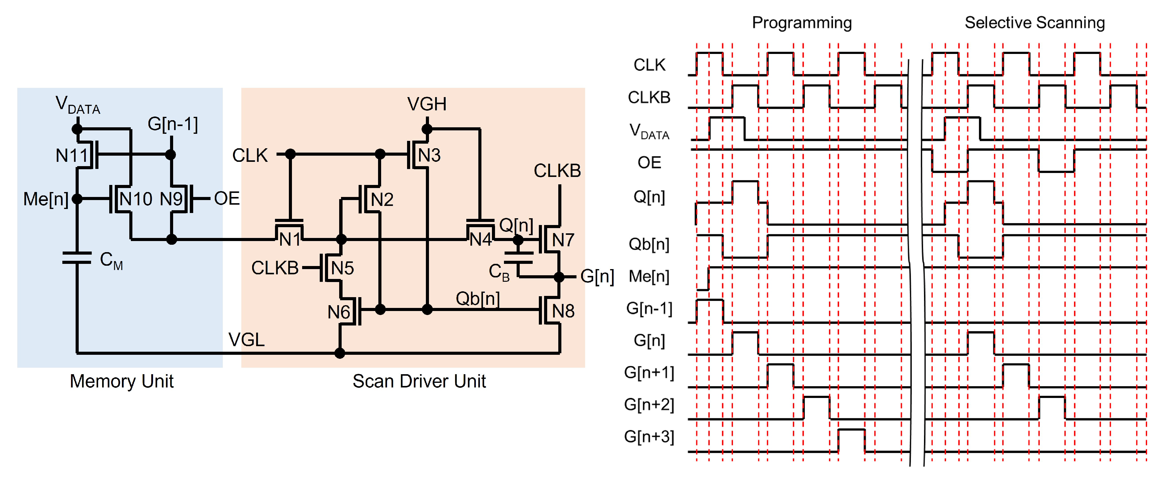
One selective scan driver is illustrated in Figure 24 that consists of memory unit and scan driver unit. The scan driver unit is a shift register, where Q[n] can be pre-charged by G[n-1] as well as through N9 and N10, respectively. Since the Programming period maintains OE at the high level, Q[n] is pre-charged by G[n-1], resulting in the generation of all scanning pulses. When the high pulse of is applied at a (n-1)-th line timing of the high G[n-1] pulse, a Me[n]-node is charged to the high voltage held at Cm, turning N10 on in the n-th circuit. Since the following frame does not apply a start pulse to the first stage, the scanning pulses do not take place. But when the high pulse of and low pulse of OE are applied, the n-th shift register with the high voltage Me[n]-node pre-charges Q[n] and generates the high pulse of G[n]. Consequently, the following stages give rise to consecutive pulses until another low pulse of OE is applied. Since this low OE pulse blocks the input signal (G[n-1]) from the previous shift register by turning N9 off, output pulses are not produced any more. Therefore, the specific pulse generation region is programmed and the remaining region is displayed by the pixel data updated in the previous frame without scanning pulses.
4. Conclusions and Future Directions
This paper describes a variety of technologies for the TFT shift register that is a key circuit block of the gate driver circuit integrated in display panels to reduce the manufacturing cost. Those technologies cover TFT backplanes, reliability improvement, depletion-mode TFT compensation, circuit area reduction, and low power consumption. In addition, it deals with the circuit implementations included in the gate driver for other functionalities such as emission pulse generation, multi-line driving scheme, noise reduction on touch sensing, random sensing pulse generation, and adaptive scanning region control.
Many researches have continued to improve these kinds of technologies further towards longer reliability, smaller circuit area, lower power consumption, and new TFT backplanes. Recently, the low temperature poly-crystalline oxide (LTPO) TFT backplane has been developed to leverage the low leakage current of oxide TFTs and the high mobility of LTPS TFTs at the same time [138,139,140,141]. Some papers about the simple and high performance shift registers implemented with LTPO TFTs can be found in well-known circuit-related journals [142,143,144,145].
On top of the main function to display images on the screen, more efforts have made good progress on integrating additional functions in display panels such as image sensing [146,147,148], fingerprint sensing [149,150,151,152,153,154], temperature sensing [155,156,157,158,159], visible light communication [160,161,162,163], and actuators for haptic applications [164]. To support these diverse functions as well as the display scanning, the demands for the higher flexibility in gate driver circuits is going to increase.
These continuous advancements of devices and circuits will pave the bright way to the future of the displays.
Author Contributions
Conceptualization, H.N. and M.K.C.; writing—original draft preparation, H.N., M.K.C., S.J. and D.K.; writing—review and editing, H.N., M.K.C. and D.K.; visualization, S.J.; supervision, H.N.; funding acquisition, H.N. All authors have read and agreed to the published version of the manuscript.
Funding
This work was supported by the Technology Innovation Program (20016317, On-Panel Circuit Integration and Driving System Technology for 1270 ppi Low-Power OLED Dislay Based on Oxide Semiconductor) funded by the Ministry of Trade Industry & Energy (MOTIE, Korea) and the Brain Korea 21 Four Program in 2022. The EDA tool was supported by the IC Design Education Center (IDEC), Korea.
Institutional Review Board Statement
Not applicable.
Informed Consent Statement
Not applicable.
Data Availability Statement
Data sharing is not applicable.
Conflicts of Interest
The authors declare no conflicts of interest.
References
- Kim, S. S.; Berkeley, B. H.; Kim, K.-H.; Song, J. K. New technologies for advanced LCD-TV performance. J. Soc. Inf. Disp. 2004, 12, 353–359. [Google Scholar] [CrossRef]
- Ishii, Y. The World of Liquid-Crystal Display TVs—Past, Present, and Future. J. Disp. Technol. 2007, 3, 351–360. [Google Scholar] [CrossRef]
- Nam, H.; Oh, K. Y.; Lee, S.-W. CCFL backlight solution for low-cost liquid crystal televisions without image artifacts. IEEE Trans. Consum. Electron. 2009, 55, 1021–1027. [Google Scholar] [CrossRef]
- Nam, H.; Lee, S.-W. Dithering artifacts in liquid crystal displays and analytic solution to avoid them. IEEE Trans. Consum. Electron. 2009, 55, 2211–2215. [Google Scholar] [CrossRef]
- Okumura, H. Birth of the Innovative Overdrive Technology for Liquid Crystal: Paving the Way for Practical Use of LCD Televisions. IEEE Consum. Electron. Mag. 2021, 10, 90–96. [Google Scholar] [CrossRef]
- Gao, Z.; Ning, H.; Yao, R.; Xu, W.; Zou, W.; Guo, C.; Luo, D.; Xu, H.; Xia, J. Mini-LED Backlight Technology Progress for Liquid Crystal Display. Crystals 2022, 12, 313. [Google Scholar] [CrossRef]
- Yin, K.; Hsiang, E.-L.; Zou, J.; Li, Y.; Yang, Z.; Yang, Q.; Lai, P.-C.; Lin, C.-L.; Wu, S.-T. Advanced liquid crystal devices for augmented reality and virtual reality displays: principles and applications. Light:Sci. Appl. 2022, 11, 161. [Google Scholar] [CrossRef] [PubMed]
- Geffroy, B.; le Roy, P.; Prat, C. Organic light-emitting diode (OLED) technology: materials, devices and display technologies. Polym. Int. 2006, 55, 572–582. [Google Scholar] [CrossRef]
- Nam, H.; Jeong, H. Data Supply Voltage Reduction Scheme for Low-Power AMOLED Displays. ETRI J. 2012, 34, 727–733. [Google Scholar] [CrossRef]
- Hong, G.; Gan, X.; Leonhardt, C.; Zhang, Z.; Seibert, J.; Busch, J. M.; Brase, S. A Brief History of OLEDs— Emitter Development and Industry Milestones. Adv. Mater. 2021, 33, 2005630. [Google Scholar] [CrossRef]
- Shin, H.-J.; Choi, S.-H.; Kim, D.-M.; Han, S.-E.; Bae, S.-J.; Park, S.-K.; Kim, H.-S.; Oh, C.-H. A Novel 88-inch 8K OLED Display for Premium Large-Size TVs. Proceedings of SID Display Week Symposium, Online, 17–21 May 2021; pp. 611–614. [Google Scholar]
- Seong, G.; Lee, Y.; Kwak, Y. Image Quality Comparison between LCD and OLED Display. Proceedings of Electronic Imaging, Online, 18–25 January 2021; p. 326. [Google Scholar]
- Prabha, A. Power Saving and Optimization of OLED Displays for Better System Design: A Survey. Proceedings of International Conference on Innovative Practices in Technology and Management, Pradesh, India, 22–24 February 2023. [Google Scholar]
- Lee, V. W.; Twu, N.; Kymissis, I. Micro-LED Technologies and Applications. Inf. Disp. 2016, 32, 16–23. [Google Scholar] [CrossRef]
- Wu, T.; Sher, C.-W.; Lin, Y.; Lee, C.-F.; Liang, S.; Lu, Y.; Chen, S.-W. H.; Guo, W.; Kuo, H.-C.; Chen, Z. Mini-LED and Micro-LED: Promising Candidates for the Next Generation Display Technology. Appl. Sci. 2018, 8, 1557. [Google Scholar] [CrossRef]
- Jung, T.; Choi, J. H.; Jang, S. H.; Han, S. J. Review of Micro-light-emitting-diode Technology for Micro-display Applications. Proceedings of SID Display Week Symposium, San Jose, CA, USA, 12–17 May 2019; pp. 442–446. [Google Scholar]
- Huang, Y.; Hsiang, E.-L.; Deng, M.-Y.; Wu, S.-T. Mini-LED, Micro-LED and OLED displays: present status and future perspectives. Light:Sci. Appl. 2020, 9, 105. [Google Scholar] [CrossRef] [PubMed]
- Anwar, A. R.; Sajjad, M. T.; Johar, M. A.; Hernandez-Gutierrez, C. A.; Usman, M.; Lepkowski, S. P. Recent Progress in Micro-LED-Based Display Technologies. Laser Photonics Rev. 2022, 16, 2100427. [Google Scholar] [CrossRef]
- Ryu, J.-E.; Park, S.; Park, Y.; Ryu, S.-W.; Hwang, K.; Jang, H. W. Technological Breakthroughs in Chip Fabrication, Transfer, and Color Conversion for High-Performance Micro-LED Displays. Adv. Mater. 2022, 35, 2204947. [Google Scholar] [CrossRef] [PubMed]
- Rahman, R.; Wood, M. E.; Qian, L.; Price, C. L.; Johnson, A. A.; Osgood, G. M. Head-Mounted Display Use in Surgery: A Systematic Review. Surgical Innovation 2020, 27, 88–100. [Google Scholar] [CrossRef]
- Kawanishi, H.; Onuma, H.; Maegawa, M.; Ono, T.; Akase, S.; Yamaguchi, S.; Momotani, N.; Fujita, Y.; Kondoh, Y.; Kubota, K.; Yoshida, T.; Ikawa, Y.; Ono, T.; Higashisaka, H.; Hirano, Y.; Anzai, S. High-resolution and high-brightness full-colour “Silicon Display” for augmented and mixed reality. J. Soc. Inf. Disp. 2021, 29, 57–67. [Google Scholar] [CrossRef]
- Cheng, D.; Wang, Q.; Liu, Y.; Chen, H.; Ni, D.; Wang, X.; Yao, C.; Hou, Q.; Hou, G.; Wang, Y. Design and manufacture AR head-mounted displays: A review and outlook. Light Adv. Manuf. 2021, 2, 350–369. [Google Scholar] [CrossRef]
- Chung, J.-M. Emerging Metaverse XR and Video Multimedia Technologies; Apress: Berkeley, CA, USA, 2022; pp. 99–139. [Google Scholar]
- Broll, W.; Grimm, P.; Herold, R.; Reiners, D.; Cruz-Neira, C. VR/AR Output Devices. In Virtual and Augmented Reality (VR/AR); Doerner, R., Broll, W., Grimm, P., Jung, B., Eds.; Springer: New York, USA, 2022; pp. 149–200. [Google Scholar]
- Miao, W.-C.; Hsiao, F.-H.; Sheng, Y.; Lee, T.-Y.; Hong, Y.-H.; Tasi, C.-W.; Chen, H.-L.; Liu, Z.; Lin, C.-L.; Chung, R.-J.; Ye, Z.-T.; Horng, R.-H.; Chen, S.-C.; Kuo, H.-C.; He, J.-H. Microdisplays: Mini-LED, Micro-OLED, and Micro-LED. Adv. Opt. Mater. 2023, 12, 2300112. [Google Scholar] [CrossRef]
- Blankenbach, K. LCD Innovations vs. OLED Performance for Automotive Applications. In Proceedings of SID Display Week Symposium, Los Angeles, CA, USA, 21–26 May 2023; pp. 327–330. [Google Scholar]
- Tian, D.; Ma, H.; Huang, G.; Gao, M.; Cai, F.; Fang, Y.; Li, C.; Jiang, X.; Wang, A.; Wang, S.; Du, Z. A Review on Quantum Dot Light-Emitting Diodes: From Materials to Applications. Adv. Opt. Mater. 2023, 11, 2201965. [Google Scholar] [CrossRef]
- Wu, S. Y.-X. The Future of Automotive Displays and Technology: A Look Ahead. Proceedings of International Workshop on Active-Matrix Flatpanel Displays and Devices, Kyoto, Japan, 04–07 July 2023. [Google Scholar]
- Kim, J. H.; Pyun, Y. J.; Oh, J. H.; Song, K. H.; Kim, Y. N.; Cho, J. H.; Yoon, C. Y.; Han, Y. H.; Nam, H. Low Complexity Local Dimming Algorithm for High Quality Head Up Displays in Automotive Vehicles. J. Inf. Disp., 2024, 25, 197–210. [Google Scholar] [CrossRef]
- Ruckmongathan, T. N. Driving matrix liquid crystal displays. Pramana - J. Phys. 1999, 53, 199–212. [Google Scholar] [CrossRef]
- Hunze, A.; Scheffel, M.; Birnstock, J.; Blassing, J.; Kanitz, A.; Rajoelson, S.; Rogler, W.; Wittmann, G.; Hartmann, H.; Winnacker, A. Passive Matrix Displays Based on the New Red Emitting Dopant RedATDB. Proceedings of SID Display Week Symposium, Boston, MA, USA, 19–24 May 2002; pp. 1186–1189. [Google Scholar]
- Xiong, S.; Guo, B.; Wu, C.; Chen, Y.; Hao, Y.; Zhou, Z.; Yang, H. A Novel Design of Sub-frame and Current Driving Method for PM-OLED. Proceedings of SID Display Week Symposium, Boston, MA, USA, 19–24 May 2002; pp. 1174–1177. [Google Scholar]
- Ohta, S.; Chuman, T.; Miyaguchi, S.; Satoh, H.; Tanabe, T.; Okuda, Y.; Tsuchida, M. Active Matrix Driving Organic Light-Emitting Diode Panel Using Organic Thin-Film Transistors. Jpn. J. Appl. Phys. 2005, 44, 3678. [Google Scholar] [CrossRef]
- Park, I.-S.; Kim, T.-W.; Lee, J.-Y.; Choi, B.-D. Data driver architecture and driving scheme of AMOLED microdisplay for mobile projectors. IEEE Trans. Consum. Electron. 2009, 55, 2365–2371. [Google Scholar] [CrossRef]
- Blankenbach, K. Active Matrix Driving. In Handbook of Visual Display Technology; Chen, J., Cranton, W., Fihn, M., Eds.; Springer: Berlin, Heidelberg, Germany, 2012; pp. 441–458. [Google Scholar]
- Keum, N.-H.; Oh, K.; Hong, S.-K.; Kwon, O.-K. A Pixel Structure Using Block Emission Driving Method for High Image Quality in Active Matrix Organic Light-Emitting Diode Displays. J. Disp. Technol. 2016, 12, 1250–1256. [Google Scholar] [CrossRef]
- Kim, H.-S.; Kim, D.-K. An Active-Matrix OLED Driver CMOS IC With Compensation of Non-Uniform Routing-Line Resistances in Ultra-Thin Panel Bezel. IEEE J. Solid-State Circuits 2017, 53, 484–500. [Google Scholar] [CrossRef]
- How To Drive Displays. Available online: https://rdotdisplays.com/articles/how-to-drive-displays (accessed on 10 March 2024).
- Hsia, S.-C.; Sheu, M.-H.; Chen, B.-Y. Area-efficient multi-channel active matrix micro-LED driver chip design. Analog Integr. Circ. Sig. Process. 2022, 111, 137–152. [Google Scholar] [CrossRef]
- 263 / 256 Channel TFT-LCD Gate Driver. Available online: https://pdf1.alldatasheet.com/datasheet-pdf/view/37875/SAMSUNG/S6C0657.html (accessed on 10 March 2024).
- den Boer, W. Select Line Driver for the Offset-Scan-and-Hold Dual Select Diode AMLCDs. Proceedings of SID Display Week Symposium, San Jose, CA, USA, 3–8 June 2001; pp. 44–47. [Google Scholar]
- Kudo, Y.; Akai, A.; Furuhashi, T.; Atsudo, T.; Okota, Y. Low-power and High-integration Driver IC for Small-sized TFT-LCDs. Proceedings of SID Display Week Symposium, Baltimore, MD, USA, 18–23 May 2003; pp. 1244–1247. [Google Scholar]
- Shift Registers in Digital Logic. Available online: https://www.geeksforgeeks.org/shift-registers-in-digital-logic/ (accessed on 10 March 2024).
- Jeon, J.; Choo, K.-S.; Lee, W.-K.; Song, J.-H.; Kim, H.-G. Integrated a-Si Gate Driver Circuit for TFT-LCD Panel. Proceedings of SID Display Week Symposium, Seattle, WA, USA, 23–28 May 2004; pp. 10–13. [Google Scholar]
- Ha, Y.-M.; Hong, S.-K.; Jeong, H.; Park, J.-D.; Kim, B.-K.; Kim, W.-Y. P-type Low-Power Low-Temperature TFT-LCDs. Proceedings of SID Display Week Symposium, Seattle, WA, USA, 23–28 May 2004; pp. 1080–1083. [Google Scholar]
- Nam, W.-J.; Jung, S.-H.; Lee, J.-H.; Lee, H.-J.; Han, M.-K. A Low-Voltage P-type Poly-Si Integrated Driving Circuits for Active Matrix Display. Proceedings of SID Display Week Symposium, Boston, MA, USA, 24–27 May 2005; pp. 1046–1049. [Google Scholar]
- Lee, Y. S.; Park, H. W.; Moon, S.-H.; Kim, T.; Lee, K.-C.; Berkeley, B. H. ; Kim. S.-S. Advanced TFT-LCD Data Line Reduction Method. In Proceedings of SID Display Week Symposium, San Francisco, CA, USA, 4–6 June 2006; pp. 1083–1086. [Google Scholar]
- Yeh, S.-H.; Sun, W.-T.; Pai, C.-C.; Chou, H.-S.; Yang, C.-S. System-on-Glass LTPS LCD using P-type TFTs. Proceedings of SID Display Week Symposium, San Francisco, CA, USA, 4–6 June 2006; pp. 1177–1180. [Google Scholar]
- Ibaraki, N. a-Si TFT technologies for large-size and high-pixel-density AM-LCDs. Mater. Chem. Phys. 1996, 43, 220–226. [Google Scholar] [CrossRef]
- Nathan, A.; Servati, P.; Karim, K. S. TFT circuit integration in a-Si:H technology. Proceedings of International Conference on Microelectronics, Nis, Yugoslavia, 12–15 May 2002. [Google Scholar]
- Li, J.; Bansal, A.; Roy, K. Poly-Si Thin-Film Transistors: An Efficient and Low-Cost Option for Digital Operation. IEEE Trans. Electron Devices 2007, 54, 2918–2929. [Google Scholar] [CrossRef]
- Lih, J.-J.; Sung, C.-F.; Li, C.-H.; Hsiao, T.-H.; Lee, H.-H. Comparison of a-Si and Poly-Si for AMOLED displays. J. Soc. Inf. Disp. 2012, 12, 367–371. [Google Scholar] [CrossRef]
- Kamiya, T.; Nomura, K.; Hosono, H. Present status of amorphous In–Ga–Zn–O thin-film transistors. Sci. Technol. Adv. Mater. 2010, 11, 044305. [Google Scholar] [CrossRef] [PubMed]
- Fortunato, E.; Barquinha, P.; Martins, R. Oxide Semiconductor Thin-Film Transistors: A Review of Recent Advances. Adv. Mater. 2012, 24, 2945–2986. [Google Scholar] [CrossRef] [PubMed]
- Kuo, Y. Thin Film Transistor Technology—Past, Present, and Future. Electrochem. Soc. Interface 2013, 22, 55. [Google Scholar] [CrossRef]
- Jang, J. Past, current and future TFT technologies for display manufacturing. Proceedings of International Workshop on Active-Matrix Flatpanel Displays and Devices, Kyoto, Japan, 02–05 July 2013. [Google Scholar]
- Mativenga, M.; Geng, D.; Jang, J. Oxide Versus LTPS TFTs for Active-Matrix Displays. Proceedings of SID Display Week Symposium, San Diego, CA, USA, 1–6 June 2014; pp. 1–4. [Google Scholar]
- Geng, D.; Wang, K.; Li, L.; Myny, K.; Nathan, A.; Jang, J.; Kuo, Y.; Liu, M. Thin-film transistors for large-area electronics. Nat. Electron. 2023, 6, 963–972. [Google Scholar] [CrossRef]
- Plus, D. Shift register useful as a select line scanner for liquid crystal display. US Patent 5,222,082, 1993. [Google Scholar]
- Lebrun, H.; Kretz, T.; Magarino, J.; Szydlo, N. Design of integrated Drivers with Amorphous Silicon TFTs for Small Displays. Basic Concepts. In Proceedings of SID Display Week Symposium, Boston, MA, USA, 24–27 May 2005; pp. 950–953. [Google Scholar]
- Oh, J. H.; Hur, J. H.; Son, Y. D.; Kim, K. M.; Kim, S. H. ; Kim. E. H; Choi, J. W., Hong, S. M., kim, J. O., Bae, B. S., Eds.; Jang, J. 2.0 inch a-Si: H TFT-LCD with Low Noise Integrated Gate Driver. In Proceedings of SID Display Week Symposium, Boston, MA, USA, 27 May 2005; pp. 942–945. [Google Scholar]
- Kim, C.-H.; Yoo, S.-J.; Kim, H.-J.; Jun, J.-M.; Lee, J.-Y. Integrated a-Si TFT row driver circuits for high-resolution applications. J. Soc. Inf. Disp. 2006, 14, 333–337. [Google Scholar] [CrossRef]
- Nam, H.; Song, E. Oxide TFT inverter with wide output dynamic range. Electron. Lett. 2012, 48, 791–792. [Google Scholar] [CrossRef]
- Song, E.; Nam, H. Shoot-through current reduction scheme for low power LTPS TFT programmable shift register. J. Soc. Inf. Disp. 2014, 22, 18–22. [Google Scholar] [CrossRef]
- Liu, S.-E.; Kung, C.-P.; Hou, J. Estimate Threshold Voltage Shift in a-Si:H TFTs Under Increasing Bias Stress. IEEE Trans. Electron Devices 2009, 56, 65–69. [Google Scholar] [CrossRef]
- Jeong, J. K.; Yang, H. W.; Jeong, J. H.; Mo. Y.-G.; Kim, H. D. Origin of threshold voltage instability in indium-gallium-zinc oxide thin film transistors. Appl. Phys. Lett. 2008, 93, 123508. [Google Scholar] [CrossRef]
- Wei, C.-C.; Lin, W.-C.; Lo, S.-H.; Chang, C.-J.; Wu, W.-E. Integrated Gate Driver Circuit Using a-Si TFT. Proceedings of International Display Workshops, Takamatsu, Japan, 06–09 December 2005. [Google Scholar]
- Koo, J. H.; Choi, J. W.; Kim, Y. S.; Kang, M. H.; Ahn, K. W.; Lee, S. W.; Jang, J. Nobel a-Si:H Gate Drivers with High Reliability. Proceedings of International Display Workshops, Otsu, Japan, 06–08 December 2006. [Google Scholar]
- Moon, S.-H.; Lee, Y.-S.; Lee, M.-C.; Berkeley, B. H.; Kim, N.-D.; Kim, S.-S. Integrated a-Si:H TFT Gate Driver Circuits on Large Area TFT-LCDs. Proceedings of SID Display Week Symposium, Long Beach, CA, USA, 20–25 May 2007; pp. 1478–1481. [Google Scholar]
- Shih, C. J.; Hsu, C. Y.; Kuo, C. C.; Ku, C. P.; Yu, C. K.; Tsai, C. H. 5” WQVGA a-Si TFT LCD with High Reliability Integrated Gate Driver. Proceedings of International Display Workshops, Sapporo, Japan, 05–07 December 2007. [Google Scholar]
- Hwang, I.; Moh, S.; Lee, M.-C.; Lee, E.-S. Design of Integrated a-Si Gate Driver Circuits for Low Power Consumption. Proceedings of SID Display Week Symposium, Los Angeles, CA, USA, 18–23 May 2008; pp. 842–845. [Google Scholar]
- Lin, C.-L.; Tu, C.-D.; Chuang, M.-C.; Yu, J.-S. Design of Bidirectional and Highly Stable Integrated Hydrogenated Amorphous Silicon Gate Driver Circuits. J. Disp. Technol. 2011, 7, 10–18. [Google Scholar] [CrossRef]
- Lin, C.-L.; Chen, M.-H.; Tu, C.-D.; Chuang, M.-C. Highly Reliable Integrated Gate Driver Circuit for Large TFT-LCD Applications. IEEE Electron Device Lett. 2012, 33, 679–681. [Google Scholar] [CrossRef]
- Kim, B.; Jang, Y. H.; Yoon, S. Y.; Chun, M. D.; Cho, H. N.; Cho, N. W.; Sohn, C. Y.; Jo, S. H.; Choi, S. C.; Kim, C.-D.; Chung, I.-J. a-Si Gate Driver Integration with Time Shared Data Driving. Proceedings of International Display Workshops, Takamatsu, Japan, 06–09 December 2005. [Google Scholar]
- Yoon, S. Y.; Jang, Y. H.; Kim, B.; Chun, M. D.; Cho, H. N.; Cho, N. W.; Sohn, C. Y.; Jo, S. H.; Kim, C.-D.; Chung, I.-J. Highly Stable Integrated Gate Driver Circuit using a-Si TFT with Dual Pull-down Structure. Proceedings of SID Display Week Symposium, Boston, MA, USA, 24–27 May 2005; pp. 348–351. [Google Scholar]
- Yeh, S.-H.; Sun, W.-T.; Pai, C.-C.; Chou, H.-S.; Yang, C.-S. System-on-Glass LTPS LCD using P-type TFTs. Proceedings of SID Display Week Symposium, San Francisco, CA, USA, 4–9 June 2006; pp. 1177–1180. [Google Scholar]
- Nam, W.-J.; Lee, J.-H.; Lee, H.-J.; Shin, H.-S.; Han, M.-K. Peripheral circuit designs using low-temperature p-type poly-Si thin-film transistors. J. Soc. Inf. Disp. 2006, 14, 403–409. [Google Scholar] [CrossRef]
- Zhao, L.-Q.; Wu, C.-Y.; Hao, D.-S.; Yao, Y.; Meng, Z.-G.; Xiong, S.-Z. An integrated driving circuit implemented with p-type LTPS TFTs for AMOLED. Optoelectron. Lett. 2009, 5, 104–107. [Google Scholar] [CrossRef]
- Jung, M-H. ; Chung H.-J.; Park, Y.-J.; Kim, O. A Full p-Type Poly-Si TFT Shift Register for Active Matrix Displays. MRS Online Proceedings Library 2009, 1245, 1906. [Google Scholar] [CrossRef]
- Tsai, Y.-S.; Liu, C.-Y.; Tseng, C.-C.; Shih, L.-W. A Slim Border Design for Wearable Display: Using Novel P-type Shift Register and Optimal Layout Arrangement. Proceedings of SID Display Week Symposium, San Jose, CA, USA, 31 May–4 June 2015; pp. 64–66. [Google Scholar]
- Chen, M.; Lei, J.; Huang, S.; Liao, C.; Deng, L. Poly-Si TFTs integrated gate driver circuit with charge-sharing structure. J. Semicond. 2017, 38, 055001. [Google Scholar] [CrossRef]
- Kang, C.-K.; Park, Y.-S.; Park, S.-I.; Mo, Y.-G.; Kim, B.-H.; Kim, S. S. Integrated Scan Driver with Oxide TFTs Using Floating Gate Method. Proceedings of SID Display Week Symposium, Los Angeles, CA, USA, 15–20 May 2011; pp. 25–27. [Google Scholar]
- Park, Y.-S.; Chung, B.-Y.; Kang, C.-K.; Park, S.-I.; Im, K.-J.; Jeong, J. H.; Kim, B.-H.; Kim, S. S. Oxide TFT Scan Driver with Dynamic Threshold Voltage Control. Proceedings of SID Display Week Symposium, Los Angeles, CA, USA, 15–20 May 2011; pp. 718–721. [Google Scholar]
- Kim, B.; Ryoo, C.-I.; Kim, S.-J.; Bae, J.-U.; Seo, H.-S.; Kim, C.-D.; Han, M.-K. New Depletion-Mode IGZO TFT Shift Register. IEEE Electron Device Lett. 2011, 32, 158–160. [Google Scholar] [CrossRef]
- Kim, B.; Choi, C. C.; Lee, S.-Y.; Kuk, S.-H.; Jang, Y. H.; Kim, C.-D.; Han, M. K. A Depletion-Mode a-IGZO TFT Shift Register With a Single Low-Voltage-Level Power Signal. IEEE Electron Device Lett. 2011, 32, 1092–1094. [Google Scholar] [CrossRef]
- Kim, B.; Choi, S. C.; Lee, J.-S.; Kim, S.-J.; Jang, Y.-H.; Yoon, S.-Y.; Kim, C.-D.; Han, M.-K. A Depletion-Mode In–Ga–Zn–O Thin-Film Transistor Shift Register Embedded With a Full-Swing Level Shifter. IEEE Trans. Electron Devices 2011, 58, 3012–3017. [Google Scholar] [CrossRef]
- Kim, B.; Cho, H. N.; Choi, W. S.; Kuk, S.-H.; Jang, Y. H.; Yoo, J.-S.; Yoon, S. Y.; Jun, M.; Hwang, Y.-K.; Han, M.-K. Highly Reliable Depletion-Mode a-IGZO TFT Gate Driver Circuits for High-Frequency Display Applications Under Light Illumination. IEEE Electron Device Lett. 2012, 33, 528–530. [Google Scholar] [CrossRef]
- Song, E.; Kang, B.; Han, I.; Oh, K.; Kim, B.; Nam, H. Depletion Mode Oxide TFT Shift Register for Variable Frame Rate AMOLED Displays. IEEE Electron Device Lett. 2015, 36, 247–249. [Google Scholar] [CrossRef]
- Cho, H. N.; Kim, H. Y.; Il, C. R.; Choi, S. C.; Kim, B.; Jang, Y. H.; Yoon, S. Y.; Chun, M. D.; Park, K.-S.; Moon, T.; Cho, N. W.; Jo, S. H.; Kim, S. K.; Kim, C.-D.; Kang, I. B. Amorphous-silicon gate-driver circuits of shared-node dual pull-down structure with overlapped output signals. J. Soc. Inf. Disp. 2008, 16, 77–81. [Google Scholar] [CrossRef]
- Kim, B.; Cho, H. N.; Choi, W. S.; Kuk, S.-H.; Yoo, J.-S.; Yoon, S. Y.; Jun, M.; Hwang, Y.-K.; Han, M.-K. A Novel Depletion-Mode a-IGZO TFT Shift Register With a Node-Shared Structure. IEEE Electron Device Lett. 2012, 33, 1003–1005. [Google Scholar] [CrossRef]
- Shin, H.-J.; Chang, M.-K.; Kim, Y.-H.; Choi, S.-H.; Bae, S.-J.; Shin, W.-S.; Lee, H.-W. An Improved Gate Driver Using Oxide TFTs for Large OLED Displays. Proceedings of SID Display Week Symposium, San Jose, CA, USA, 13–17 May 2024; pp. 501–504. [Google Scholar]
- Kim, Y. I.; Park, S.-J.; Nam, H. Node-sharing low-temperature poly silicon TFT shift register without bootstrapping degradation for narrow bezel displays. Electron. Lett. 2018, 54, 1162–1164. [Google Scholar] [CrossRef]
- Kim, Y. I.; Nam, H. Clocked control scheme of separating TFTs for a node-sharing LTPS TFT shift register with large number of outputs. J. Soc. Inf. Disp. 2020, 28, 825–830. [Google Scholar] [CrossRef]
- Ahn, S.-H.; Kim, E.; Jung, E. K.; Hong, S.; Im, H.; Kim, Y.-S. Indium–Gallium–Zinc Oxide Thin-Film Transistor-Based Scan Driver Circuit Using Separate Driving Structure for Multiple Output Signals. IEEE Trans. Electron Devices 2023, 70, 3605–3610. [Google Scholar] [CrossRef]
- Hack, M.; Brown, J. J.; Mahon, J. K.; Kwong, R. C.; Hewitt, R. Performance of high-efficiency AMOLED displays. J. Soc. Inf. Disp. 2001, 9, 191–195. [Google Scholar] [CrossRef]
- Kowalsky, W.; Becker, E.; Benstem, T.; Dobbertin, T.; Heithecker, D.; Johannes, H.-H.; Metzdorf, D.; Neuner, H. OLED matrix displays: technology and fundamentals. Proceedings of International IEEE Conference on Polymers and Adhesives in Microelectronics and Photonics. Incorporating POLY, PEP & Adhesives in Electronics, Potsdam, Germany, 21–24 October 2001. [Google Scholar]
- Sakariya, K.; Servati, P.; Striakhilev, D.; Nathan, A. Vt-Shift Compensating Amorphous Silicon Pixel Circuits for Flexible OLED Displays. Proceedings of MRS Fall Meeting & Exhibit, Boston, MA, USA, 1–5 December 2002. [Google Scholar]
- Sanford, J. L.; Libsch, F. R. Vt Compensated voltage-data a-Si TFT AMOLED pixel circuits. J. Soc. Inf. Disp. 2004, 12, 65–73. [Google Scholar] [CrossRef]
- Han, M.-K. AM backplane for AMOLED. Proceedings of Asian Symposium on Information Display, New Delhi, India, 8–12 October 2006. [Google Scholar]
- Lin, J.-T.; Wne, C.-N.; Lin, P.-H. A compensation threshold voltage shift pixel circuit for active matrix organic light emitting diode. Proceedings of International Conference on Microelectronics, Nis, Serbia and Montenegro, 11–14 May 2008. [Google Scholar]
- Onoyama, Y.; Yamashita, J.; Kitagawa, H.; Hasegawa, E.; Makita, A.; Yokoyama, S.; Asaki, R.; Kambe, E.; Nishimura, T.; Yamada, J.; Uchino, K.; Makimura, S.; Shiraishi, Y.; Urabes, T. 0. 5-inch XGA Micro-OLED Display on a Silicon Backplane with High-Definition Technologies. In Proceedings of SID Display Week Symposium, Boston, MA, USA, 5–8 May 2012; pp. 950–953. [Google Scholar]
- Chung, B.-Y.; Kwon, O.-K.; Matsueda, Y.; Kim, H.-D. An Emission Control Driver Using P-type TFTs for AMOLED Displays. Proceedings of International Technical Conference on Circuits/Systems, Computers and Communication, Shimonoseki, Japan, 6–9 July 2008; pp. 1009–1012. [Google Scholar]
- Song, E.; Nam, H. Programmable Pulse Width LTPS TFT Shift Register for High Resolution and High Frame Rate Active Matrix Flat Panel Displays. Proceedings of SID Display Week Symposium, Vancouver, Canada, 19–24 May 2013; pp. 473–477. [Google Scholar]
- Song, E.; Nam, H. Low Power Programmable Shift Register With Depletion Mode Oxide TFTs for High Resolution and High Frame Rate AMFPDs. J. Disp. Technol. 2014, 10, 834–838. [Google Scholar] [CrossRef]
- Song, E.; Song, S.-J.; Nam, H. Pulse-width-independent low power programmable low temperature poly-Si thin-film transistor shift register. Solid-State Electron. 2015, 107, 35–39. [Google Scholar] [CrossRef]
- Chang, M.-K.; Kim, J.-H.; Nam, H. Fine-Tunable Emission Pulse Generation Circuit Based on p-Type Low-Temperature Poly-Si Thin-Film Transistors for Active Matrix Organic Light-Emitting Diode Displays. IEEE Trans. Electron Devices 2023, 70, 3092–3099. [Google Scholar] [CrossRef]
- Lee, B.-W.; Ji, I.-H.; Han, S.-M.; Sung, S.-D.; Shin, K.-S.; Lee, J. D.; Kim, B. H.; Berkeley, B. H.; Kim, S. S. Novel Simultaneous Emission Driving Scheme for Crosstalk-free 3D AMOLED TV. Proceedings of SID Display Week Symposium, Seattle, WA, USA, 25–28 May 2010; pp. 758–761. [Google Scholar]
- Bastani, B.; Turner, E.; Vieri, C.; Jiang, H.; Funt, B.; Balram, N. Foveated pipeline for AR/VR head-mounted displays. Inf. Disp. 2017, 33, 14–35. [Google Scholar] [CrossRef]
- Bhowmik, A. K. Advances in virtual, augmented, and mixed reality technologies. Inf. Disp. 2018, 34, 18–21. [Google Scholar] [CrossRef]
- Albert, R.; Patney, A.; Luebke, D.; Kim, J. Latency requirements for foveated rendering in virtual reality. ACM Trans. Appl. Percept. 2017, 14, 1–13. [Google Scholar] [CrossRef]
- Park, S.; Kim, Y. I.; Nam, H. Foveation-based reduced resolution driving scheme for immersive virtual reality displays. Opt. Express 2019, 27, 29594. [Google Scholar] [CrossRef] [PubMed]
- Nam, H.; Kang, H. Complexity-Reduced Super Resolution for Foveation-based Driving Head Mounted Displays. IEEE Access 2021, 9, 140042–140049. [Google Scholar] [CrossRef]
- Bae, J.; Lee, J.; Nam, H. Variable Clock and EM Signal Generation Scheme for Foveation-based Driving OLED Head-Mounted Displays. Electron. 2021, 10, 538. [Google Scholar] [CrossRef]
- Sugita, Y.; Kida, K.; Yamagishi, S. In-Cell Projected Capacitive Touch Panel Technology. IEICE Trans. Electron. 1384. [Google Scholar] [CrossRef]
- Moon, S.-H.; Haruhisa, I.; Kim, K.; Park, C.-W.; Chung, H.-J.; Kim, S.-H.; Kim, B.-K.; Kim, O. Highly Robust Integrated Gate-Driver for In-Cell Touch TFT-LCD Driven in Time Division Driving Method. J. Disp. Technol. 2015, 12, 435–441. [Google Scholar] [CrossRef]
- Lin, C.-L.; Lai, P.-C.; Lai, P.-C.; Chu, T.-C.; Lee, C.-L. Bidirectional Gate Driver Circuit Using Recharging and Time-Division Driving Scheme for In-Cell Touch LCDs. IEEE Trans. Ind. Electron. 2017, 65, 3585–3591. [Google Scholar] [CrossRef]
- Seo, J.; Nam, H. Robust integrated shift register circuit over clock noises for in-cell touch applications. J. Soc. Inf. Disp. 2017, 25, 537–543. [Google Scholar] [CrossRef]
- Seo, J.; Nam, H. Low power and low noise shift register for in-cell touch display applications. IEEE J. Electron Devices Soc. 2018, 6, 726–732. [Google Scholar] [CrossRef]
- Shen, S.; Liao, C.; Yang, J.; Jiao, H.; Zhang, S. Capacitor Reused Gate Driver for Compact In-Cell Touch Displays. IEEE J. Electron Devices Soc. 2021, 9, 533–538. [Google Scholar] [CrossRef]
- Tai, Y.-H.; Chen, B.-T.; Kuo, Y.-J.; Tsai, C.-C.; Chiang, K.-Y.; Wei, Y-J. ; Chen, H.-C. A new pixel circuit for driving organic light-emitting diode with low temperature polycrystalline silicon thin-film transistors. J. Disp. Technol. 2005, 1, 100–104. [Google Scholar] [CrossRef]
- Han, N.-K. AM backplane for AMOLED. Proceedings of Asian Symposium on Information Display (ASID), New Delhi, India, 8–12 October 2006; pp. 53–58. [Google Scholar]
- Lee, J.-H.; Nam, W.-J.; Kim, B.-K.; Choi, H.-S.; Ha, Y.-M.; Han, M.-K. A new Poly-Si TFT current-mirror pixel for active matrix organic light emitting diode. IEEE Electron Device Lett. 2006, 27, 830–833. [Google Scholar] [CrossRef]
- In, H. J.; Oh, K. H.; Lee, I.; Ryu, D. H.; Choi, S. M.; Kim, K. N.; Kim, H. D.; Kwon, O. K. An advanced external compensation system for active matrix organic light-emitting diode displays with poly-Si thin-film transistor backplane. IEEE Trans. Electron Devices 2010, 57, 3012–3019. [Google Scholar] [CrossRef]
- Song, S.-J.; Chen, Y.; Jang, J.; Nam, H. Hybrid Voltage and Current Programming Pixel Circuit for High Brightness Simultaneous Emission AMOLED Display. J. Disp. Technol. 2015, 11, 255–260. [Google Scholar] [CrossRef]
- Takasugi, S.; Shin, H.-J.; Chang, M.-K.; Ko, S.-M.; Park, H.-J.; Lee, J.-P.; Kim, H.-S.; Oh, C.-H. Advanced compensation technologies for largesized UHD OLED TVs. J. Soc. Inf. Disp. 2016, 24, 410–418. [Google Scholar] [CrossRef]
- Kwon, J.; Lee, C.; Chae, Y.; Murmann, B. Design Considerations for External Compensation Approaches to OLED Display Degradation. Proceedings of IEEE International Symposium on Circuits and Systems (ISCAS), Seville, Spain, 12–14 October 2020. [Google Scholar]
- Park, K.; Oh, S.; Choi, D.; Shin, K.; Cho, H.; Bien, F. Real-Time External Compensation System With Error Correction Algorithm for High-Resolution Mobile Displays. IEEE Trans. Circuits Syst. I: Regul. Pap. 2023, 70, 1121–1132. [Google Scholar] [CrossRef]
- Kim, I. J.; Noh, S.; Ban, M. H.; Son, K.; Han, I.; Shin, H. K.; Oh, K.; Kim, B.; Kang, I. B. Integrated gate driver circuit technology with IGZO TFT for sensing operation. J. Soc. Inf. Disp. 2019, 27, 313–318. [Google Scholar] [CrossRef]
- Kim, Y.-D.; Han, K.-L.; Park, J.-S.; Choi, B.-D. A Random Access Gate Driver Using a-IGZO TFTs for External Compensation of High-Resolution, High-Frame-Rate AMOLEDs. Proceedings of SID Display Week Symposium, San Jose, CA, USA, 8–13 May 2022; pp. 32–35. [Google Scholar]
- Nam, H.; Lee, S. W. Low-Power Liquid Crystal Display Television Panel with Reduced Motion Blur. IEEE Trans. Consum. Electron. 2010, 56, 307–311. [Google Scholar] [CrossRef]
- Yonebayashi, R.; Tanaka, K.; Okada, K.; Yamamoto, K.; Yamamoto, K.; Uchida, S.; Aoki, T.; Takeda, Y.; Furukawa, H.; Ito, K.; Katoh, H.; Nakamura, W. High refresh rate and low power consumption AMOLED panel using top-gate n-oxide and p-LTPS TFTs. Proceedings of SID Display Week Symposium, Online, 3–7 August 2020; pp. 355–358. [Google Scholar]
- You, B.; Nam, H.; Lee, H. Image Adaptive Refresh Rate Technology for Ultra Low Power Consumption. Proceedings of SID Display Week Symposium, Online, 3–7 August 2020; pp. 676–679. [Google Scholar]
- Slavenburg, G.; Janseens, M.; Lucas, L.; Schutten, R. J.; Verbeure, T. Variable Refresh Rate Displays. Proceedings of SID Display Week Symposium, Online, 3–7 August 2020; pp. 669–672. [Google Scholar]
- Kwon, S.; Kim, S.; Yoon, C.; Kim, T.; Yang, J.; Choi, Y.; Choe, W. Multi-Frequency driving of OLED for low power consumption. Proceedings of SID Display Week Symposium, San Jose, CA, USA, 8–13 May 2022; pp. 155–158. [Google Scholar]
- Jo, J.-H.; Jeong, W.-B.; Joung, Y.-S.; Lee, S.-W. Selective Scan Driver for Low-Power Consumption Using Oxide Thin Film Transistors. IEEE Electron Device Lett. 2022, 43, 1263–1266. [Google Scholar] [CrossRef]
- Yuan, Z.; Han, Y.; Meng, S.; Gu, X.; Liu, X.; Li, Y.; Xu, P.; Yuan, C.; Cheng, X.; Yan, G.; Yu, J.; Dong, X. An Innovative Decoder-type GOA for Intelligent Split-Screen and External Compensation Technology. Proceedings of SID Display Week Symposium, San Jose, CA, USA, 13–17 May 2024; pp. 513–516. [Google Scholar]
- Huang, Z.; Xu, J.; Pan, Z.; Yang, Y.; Zhang, L.; Dang, P. l Shen, Y. ; Zhu, X. Gate Driver Circuit to generating Multi-Frequency Pulses using LTPO Technology. In Proceedings of SID Display Week Symposium, San Jose, CA, USA, 13–17 May 2024; pp. 1664–1666. [Google Scholar]
- Chang, T.-K.; Lin, C.-W.; Chang, S. LTPO TFT Technology for AMOLEDs. Proceedings of SID Display Week Symposium, San Jose, CA, USA, 13–17 May 2019; pp. 545–548. [Google Scholar]
- Chung, U.-J.; Choi, S.-C.; Noh, S. Y.; Kim, K.-T.; Moon, K.-J.; Kim, J.-H.; Park, K.-S.; Choi, H.-C.; Kang, I.-B. Manufacturing Technology of LTPO TFT. Proceedings of SID Display Week Symposium, Online, 3–7 August 2020; pp. 545–548. [Google Scholar]
- Qiu, H.; An, J.; Wang, K.; Liao, C.; Dai, C.; Zhang, X.; Zhang, S. A Low Power and IR Drop Compensable AMOLED Pixel Circuit Based on Low-Temperature Poly-Si and Oxide (LTPO) TFTs Hybrid Technology. IEEE J. Electron Devices Soc. 2022, 10, 51–58. [Google Scholar] [CrossRef]
- Fu, J.; Peng, Z.; Liao, C.; Zheng, X.; An, J.; Liang, J.; Dai, C.; Zhang, X.; Zhang, S. High Performance AMOLED Pixel Circuit Using Interleaved Emit Signals Based on Low-Temperature Poly-Si and Oxide (LTPO) TFTs. Proceedings of SID Display Week Symposium, San Jose, CA, USA, 8–13 May 2022; pp. 132–135. [Google Scholar]
- An, J.; Liao, C.; Zhu, Y.; Zheng, X.; Dai, C.; Zhang, X.; Zhang, S. Gate Driver on Array With Multiple Outputs and Variable Pulse Widths for Low-Temperature Polysilicon and Oxide (LTPO) TFTs Driven AMOLED Displays. IEEE Trans. Circuits Syst. II Express Briefs 2022, 70, 934–938. [Google Scholar] [CrossRef]
- Kim, J.; Billah, M. M.; Jang, J. Ultra-Low Power, Emission Gate Driver With Pulse Width Modulation Using Low-Temperature Poly-Si Oxide Thin-Film Transistors. IEEE Electron Device Lett. 2022, 43, 236–239. [Google Scholar] [CrossRef]
- Kim, J.; Jeong, M.; Kim, B.; Jang, J. 38μm-Pitch, 3-Output Gate Driver Using Low-Temperature Poly-Si Oxide TFTs for High Resolution Display. IEEE Electron Device Lett. 2022, 43, 1471–1474. [Google Scholar] [CrossRef]
- Kim, J.; Lee, H.; Jang, J. Emission Gate Driver With Five Low-Temperature Poly-Si Oxide TFTs Without Capacitor for Narrow-Bezel AMOLED Display. IEEE J. Solid-State Circuits 2022, 6, 53–56. [Google Scholar] [CrossRef]
- Xu, Y.; Ruan, C.-P.; Zhou, L.; Zou, J.-H.; Xu, M.; Wu, W.-J.; Wang, L.; Peng, J.-B. A 256 × 256, 50-μm Pixel Pitch OPD Image Sensor Based on an IZO TFT Backplane IEEE Sensor J. 2021, 21, 20824–20832. 21. [CrossRef]
- Zhuo, R.; Lin, P.; Wu, Y.; Wu, Z.; Ye, D.; Huangfu, J. Sensorless LED display screen interaction and object recognition. J. Soc. Inf. Disp. 2021, 30, 141–158. [Google Scholar] [CrossRef]
- Yamada, N.; Nakanotani, H.; Takagi, A.; Mamada, M.; Balijapalli, U.; Ichikawa, T.; Hirata, E.; Kaizu, S.; Tanaka, A.; Itonaga, K.; Adachi, C. Three-dimensional sensing of surfaces by projection of invisible electroluminescence from organic light-emitting diodes. Sci. Adv. 2024, 10, eadj6583. [Google Scholar] [CrossRef]
- Tai, Y.-H.; Tu, C.-C.; Yuan, Y.-C.; Chang, Y.-J.; Hsu, M.-H.; Chuang, C.-Y. Light-Controlled Gap-Type TFT Used for Large-Area Under-Screen Fingerprint Sensor. IEEE J. Electron Devices Soc. 2021, 9, 517–520. [Google Scholar] [CrossRef]
- Yin, P.-H.; Lu, C.-W.; Wang, J.-S.; Chang, K.-L.; Lin, F.-K.; Chen, P. A 368 × 184 Optical Under-Display Fingerprint Sensor Comprising Hybrid Arrays of Global and Rolling Shutter Pixels With Shared Pixel-Level ADCs. IEEE J. Solid-State Circuits 2021, 56, 763–777. [Google Scholar] [CrossRef]
- Jeon, D.-H.; Jeong, W.-B.; Chung, H.-J.; Lee, S.-W. Novel Micro-LED Display Featuring Fingerprint Recognition Without Additional Sensors. IEEE Access 2022, 10, 74187–74197. [Google Scholar] [CrossRef]
- Jeon, D.-H.; Jeong, W.-B.; Lee, S.-W. Novel Active-Matrix Micro-LED Display With External Compensation Featuring Fingerprint Recognition. IEEE Electron Device Lett. 2022, 43, 1483–1486. [Google Scholar] [CrossRef]
- Sugimoto, K.; Hatsumi, R.; Nakazawa, Y.; Idojiri, S.; Kamada, T.; Kubota, D.; Okazaki, K.; Yamagata, S.; Yamazaki, S. Organic Light-Emitting Diode Display Constituted Side-by-Side OLED and Organic Photodiode Pixels Integrated in the Same Plane by Adopting MML (Metal Mask-Less Lithography) Technology. Proceedings of SID Display Week Symposium, San Jose, CA, USA, 13–17 May 2024; pp. 138–141. [Google Scholar]
- Bae, K. S.; Kim, G. H.; Park, H. A.; Park, J.; Ahn, T.; Lee, D.-Y.; Moon, S.; Kim, J.-K.; Kim, C.; Kim, Y. Full Screen Fingerprint Display with Embedded Organic Photo-detectors. Proceedings of SID Display Week Symposium, San Jose, CA, USA, 13–17 May 2024; pp. 142–145. [Google Scholar]
- Ku, N.; Hwang, J. C.; Oh, B.; Park, J.-U. Smart Sensing Systems Using Wearable Optoelectronics. Adv. Intell. Syst. 2020, 2, 1900144. [Google Scholar] [CrossRef]
- Chen, Y.; Lee, S.; Kim, H.; Lee, J.; Geng, D.; Jang, J. In-pixel temperature sensor for high-luminance active matrix micro-light-emitting diode display using low-temperature polycrystalline silicon and oxide thin-film-transistors. J. Soc. Inf. Disp. 2020, 28, 528–534. [Google Scholar] [CrossRef]
- Mu, G.; Rao, T.; Qi, Y.; Ma, S.; Hao, Q.; Chen, M.; Tang, X. Color-Tunable Organic Light-Emitting Displays for Interactive Multi-Signal Visualization. Adv. Funct. Mater. 2023, 33, 2301280. [Google Scholar] [CrossRef]
- Miao, W.-C.; Hsiao, F.-H.; Sheng, Y.; Lee, T.-Y.; Hong, Y.-H.; Tsai, C.-W.; Chen, H.-L.; Liu, Z.; Lin, C.-L.; Chung, R.-J.; Ye, Z.-T.; Horng, R.-H.; Chen, S.-C.; Kuo, H.-C.; He, J.-H. Microdisplays: Mini-LED, Micro-OLED, and Micro-LED. Adv. Opt. Mater. 2023, 12, 2300112. [Google Scholar] [CrossRef]
- Yu, S.; Park, T. H.; Jiang, W.; Lee, S. W.; Kim, E. H.; Lee, S.; Park, J.-E.; Park, C. Soft Human–Machine Interface Sensing Displays: Materials and Devices. Adv. Mater. 2023, 35, 2204964. [Google Scholar] [CrossRef]
- Ye, H.; Wang, Q. SpiderWeb: Enabling Through-Screen Visible Light Communication. In Proceedings of the ACM Conference on Embedded Networked Sensor Systems, Coimbra, Portugal, 15–17 November 2021; pp. 316–328. [Google Scholar]
- Chaleshtori, Z. N.; Zvanovec, S.; Ghassemlooy, Z.; Khalighi, M.-A. Visible light communication with OLEDs for D2D communications considering user movement and receiver orientations. Appl. Opt. 2022, 61, 676–682. [Google Scholar] [CrossRef] [PubMed]
- Hu, L.; Choi, J.; Hwangbo, S.; Kwon, D.-H.; Jang, B.; Ji, S.; Kim, J.-H.; Han, S.-K.; Ahn, J.-H. Flexible micro-LED display and its application in Gbps multi-channel visible light communication. npj Flex. Electron. 2023, 6, 100. [Google Scholar] [CrossRef]
- Zhao, Z.; Qiu, Y.; Zou, G.; Weng, J.; Yang, B.-R.; Qin, Z. Mini-LED LCDs Integrated with High-capacity MIMO Visible Light Communication. Proceedings of SID Display Week Symposium, San Jose, CA, USA, 13–17 May 2024; pp. 212–215. [Google Scholar]
- Sung, S. H.; Kho, Y.-S.; Park, S. 60kHz Ultrasonic Actuators for Animal-Friendly Haptic Displays. Proceedings of SID Display Week Symposium, San Jose, CA, USA, 13–17 May 2024; pp. 1338–1340. [Google Scholar]
Figure 1.
Concept diagram of scanning pulse generation with one-type TFTs
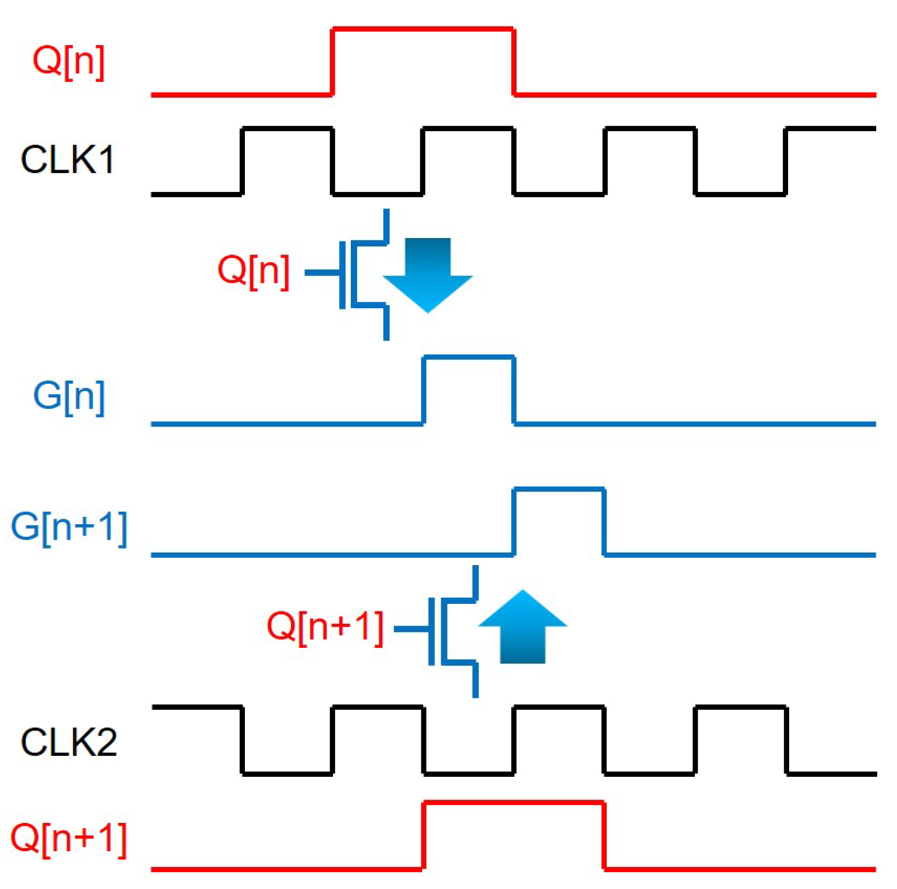
Figure 2.
Schematic and timing diagram of a basic shift register at a n-type TFT backplane
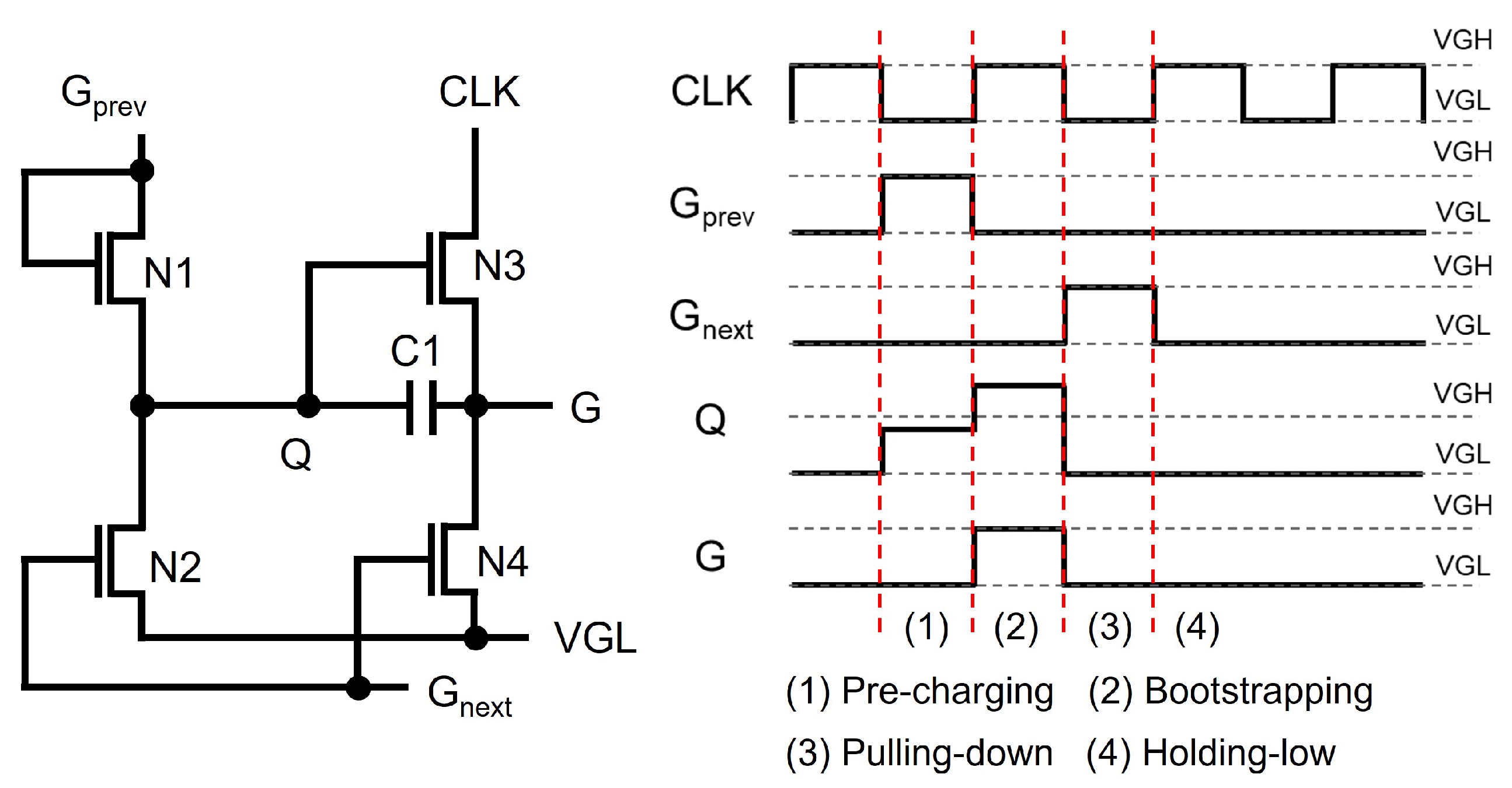
Figure 3.
Signal connections between basic shift registers
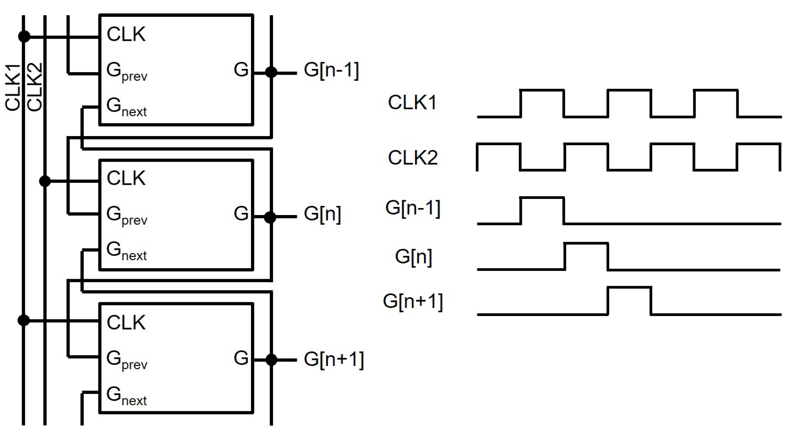
Figure 4.
Fluctuation-reduced shift register by applying another high floating node voltage to the gate nodes of pulling-down TFTs.
Figure 4.
Fluctuation-reduced shift register by applying another high floating node voltage to the gate nodes of pulling-down TFTs.
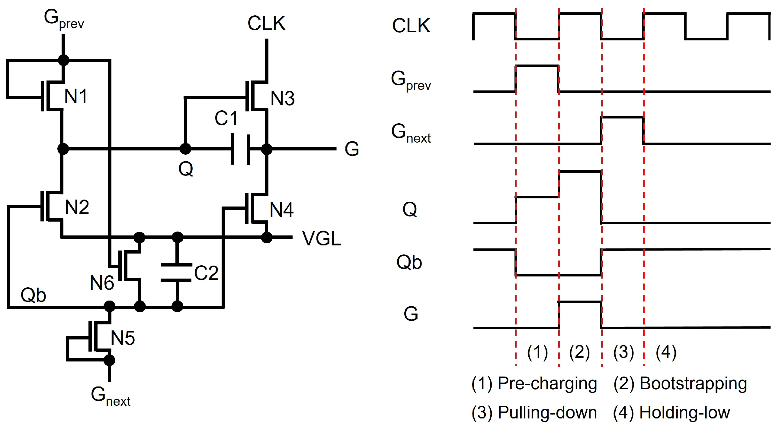
Figure 5.
Fluctuation-reduced shift register by including an internal inverter to generate Qb.
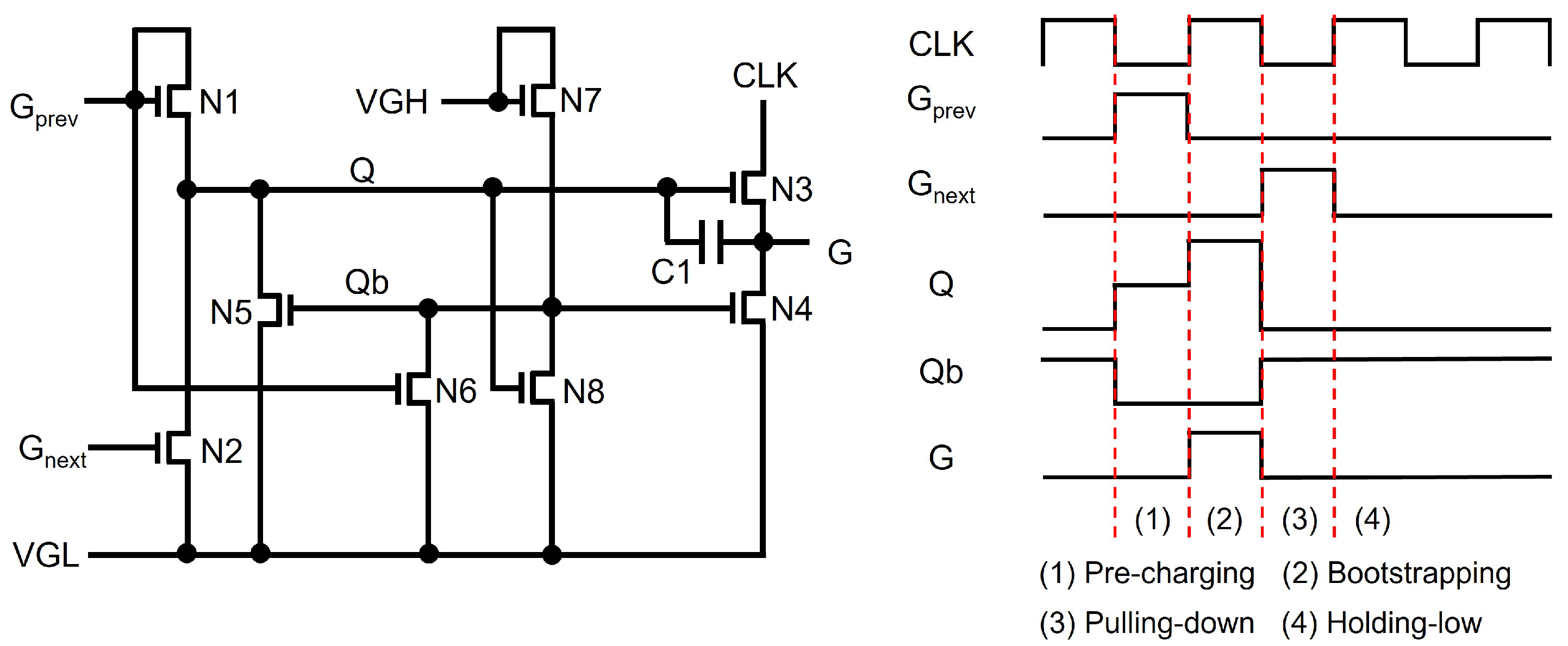
Figure 6.
Low power shift register by removing the shoot-through current path in an internal inverter.[65]
Figure 6.
Low power shift register by removing the shoot-through current path in an internal inverter.[65]
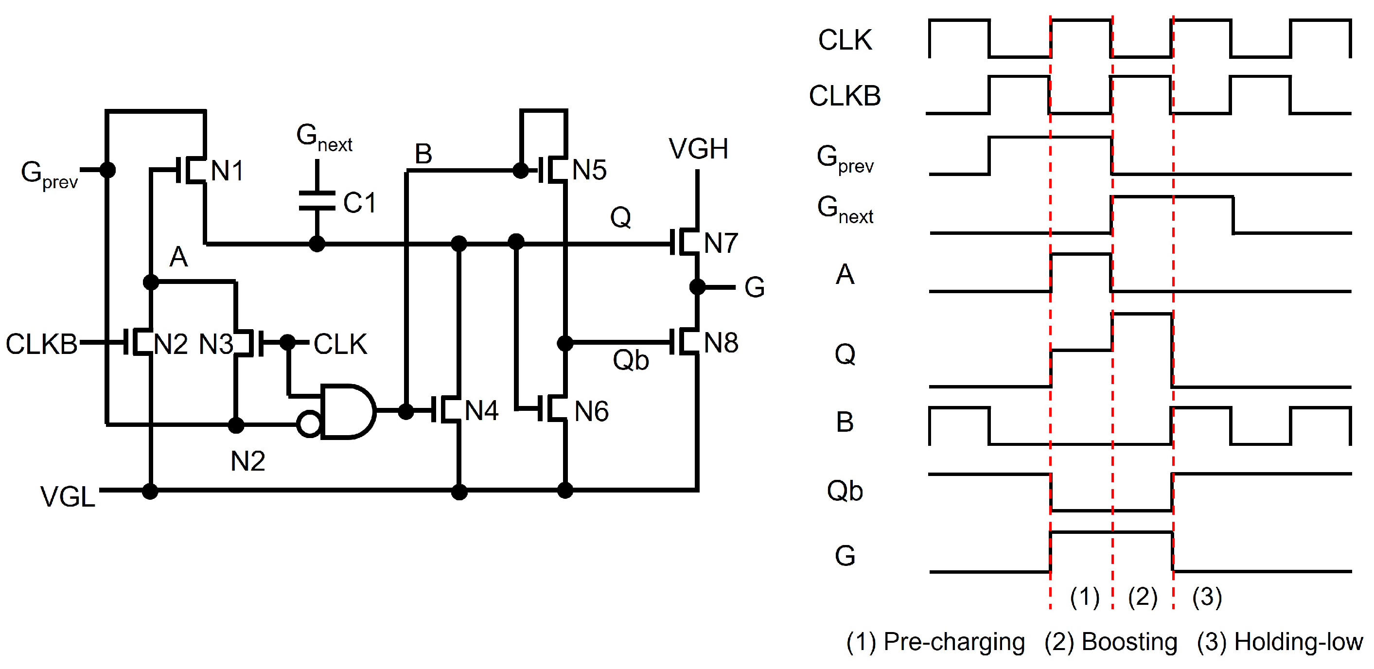
Figure 7.
Reliability-enhanced shift register by the line-by-line alternation of discharging paths for Q and G [69]
Figure 7.
Reliability-enhanced shift register by the line-by-line alternation of discharging paths for Q and G [69]
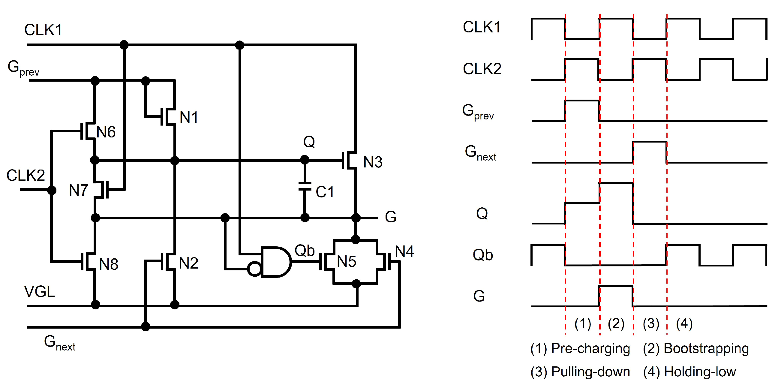
Figure 8.
4 phase clock shift register for reliability enhancement and power reduction [72]
Figure 8.
4 phase clock shift register for reliability enhancement and power reduction [72]
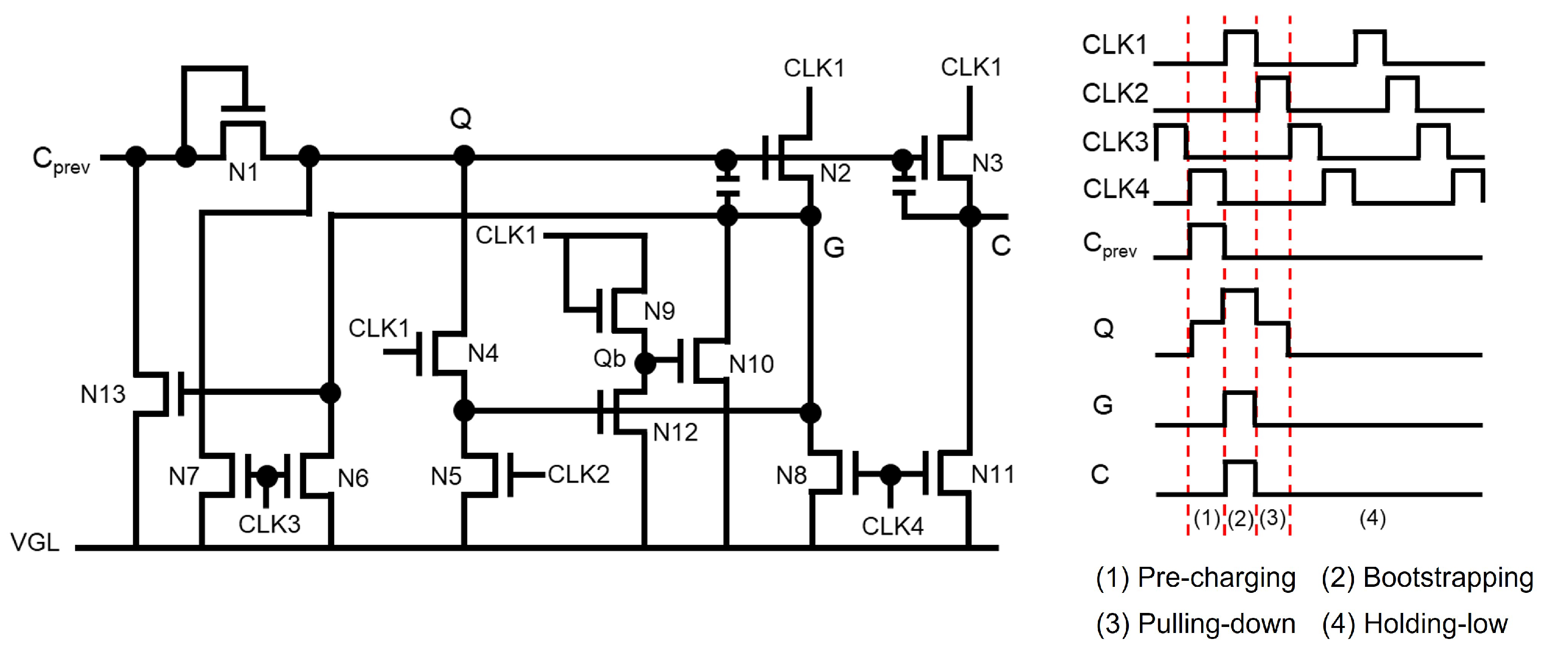
Figure 9.
Reliability-enhanced shift register by the frame-by-frame alternation of discharging paths for Q and G
Figure 9.
Reliability-enhanced shift register by the frame-by-frame alternation of discharging paths for Q and G
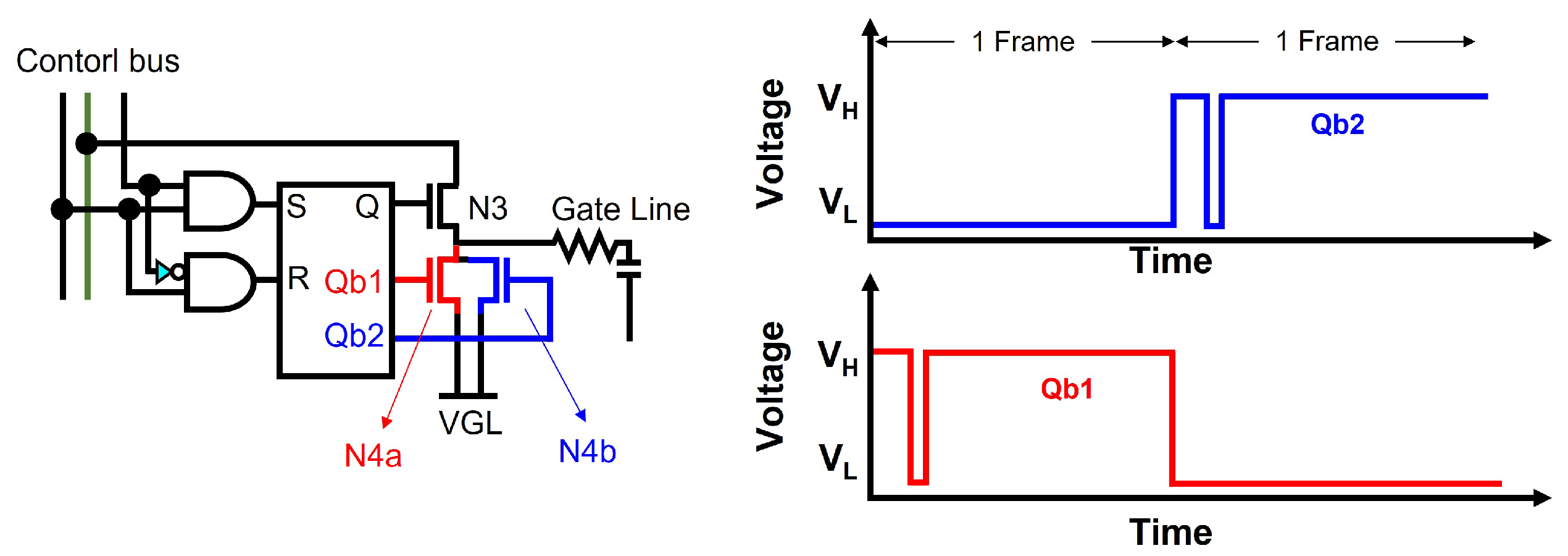
Figure 10.
Shift register based on p-type TFTs [80]
Figure 10.
Shift register based on p-type TFTs [80]
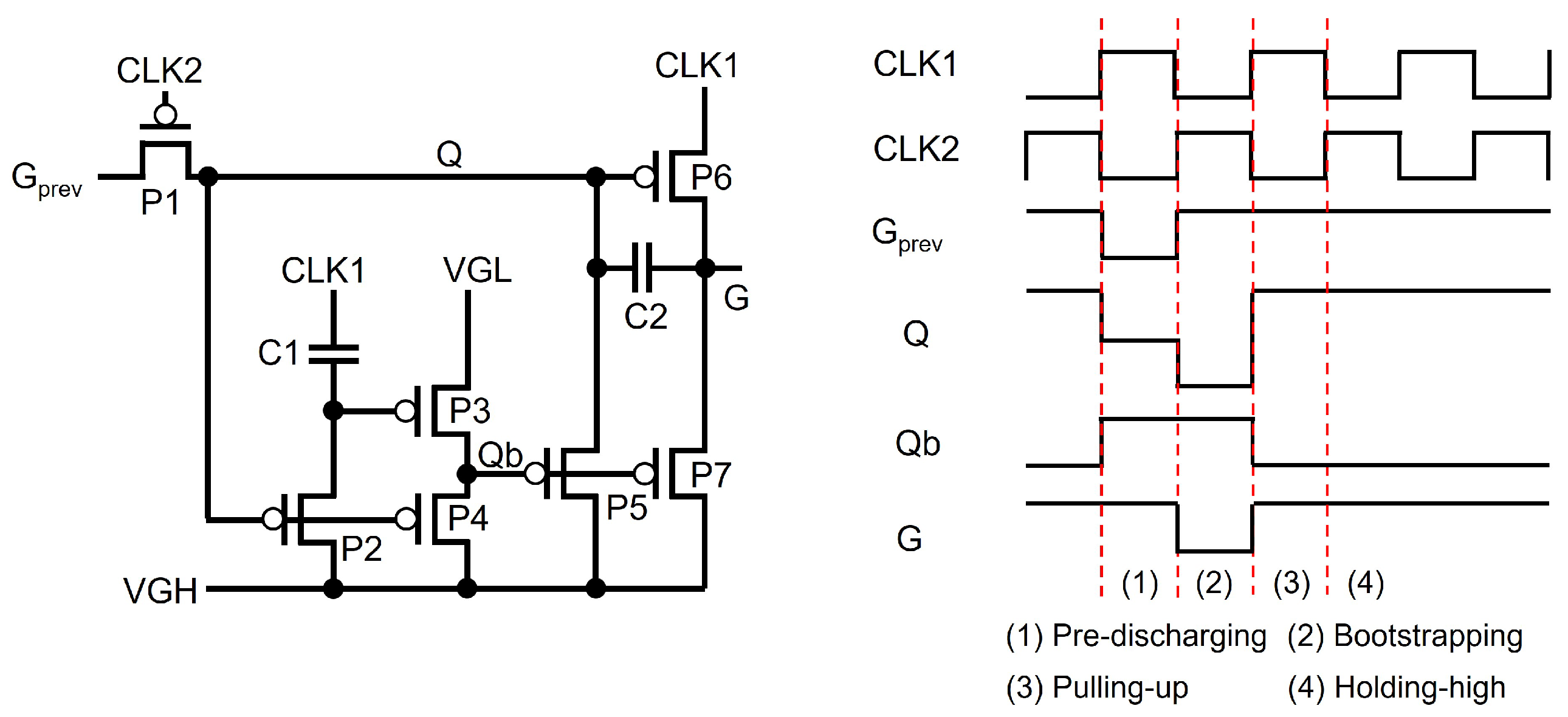
Figure 11.
Approaches to deal with depletion-mode TFTs
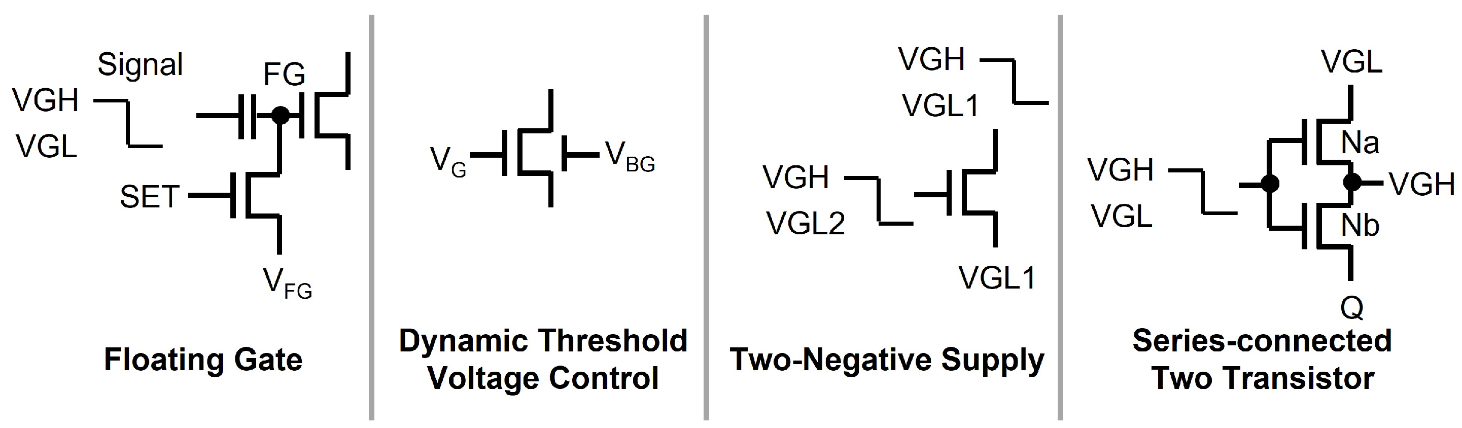
Figure 12.
Shift register based on n-type oxide TFTs [84]
Figure 12.
Shift register based on n-type oxide TFTs [84]
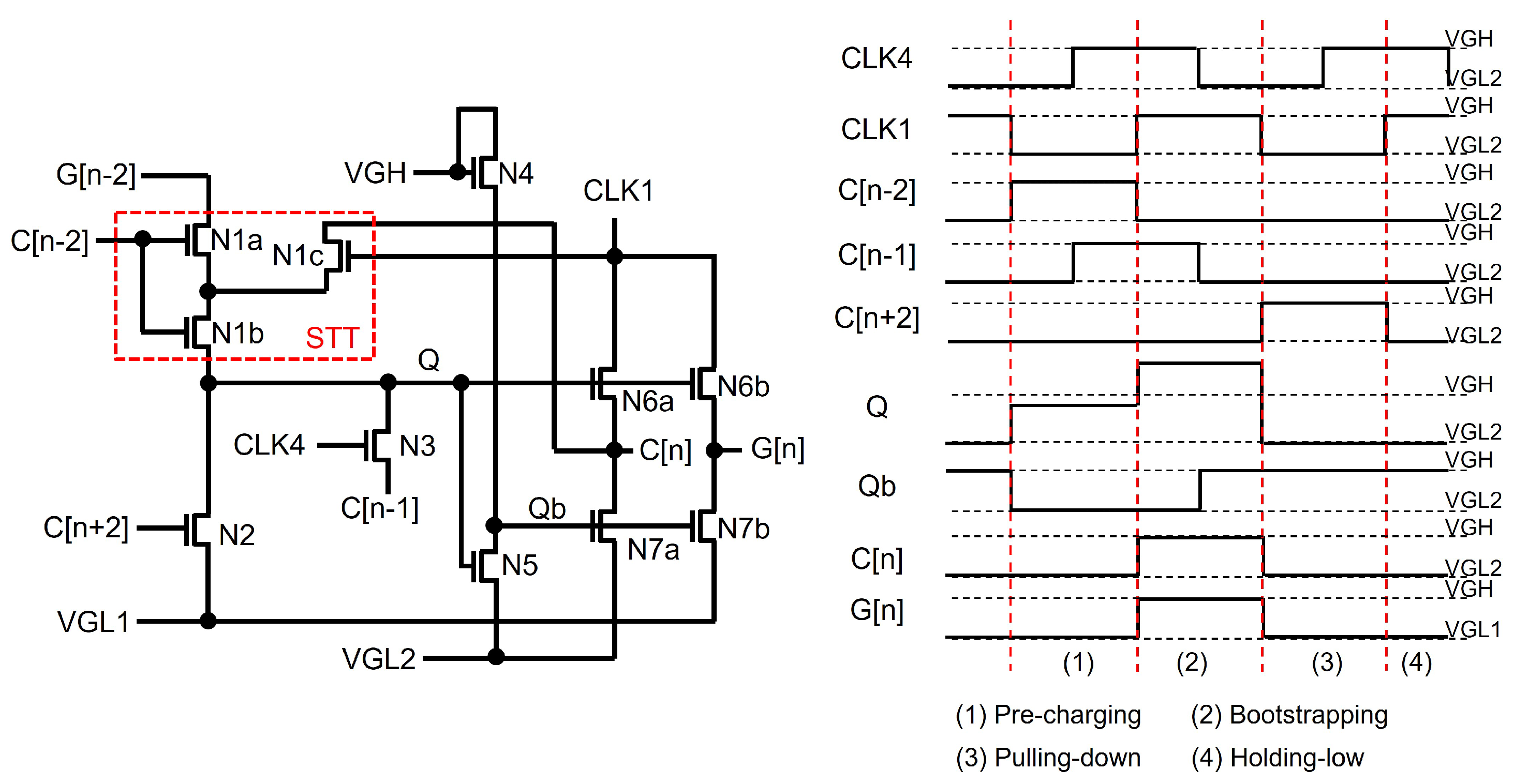
Figure 13.
Small area shift register with a Qb-sharing structure [89]
Figure 13.
Small area shift register with a Qb-sharing structure [89]
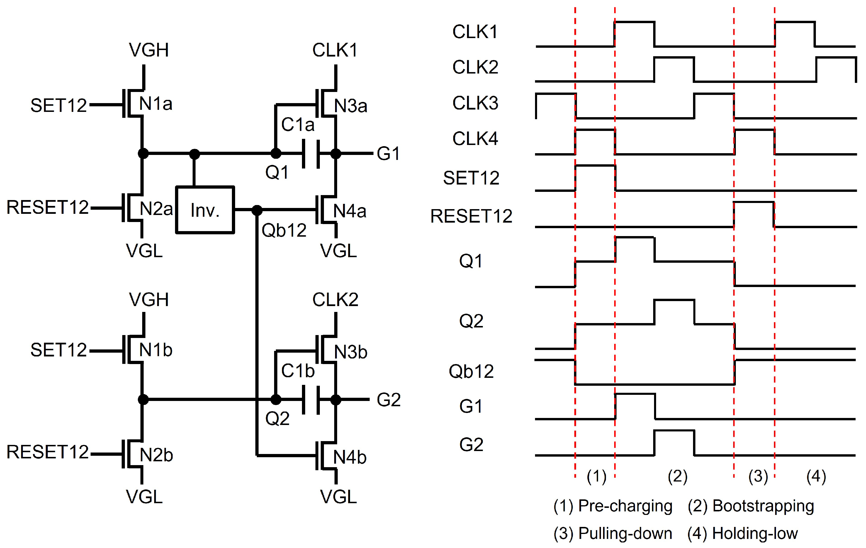
Figure 14.
Small area shift register with a direct Q-sharing structure [90]
Figure 14.
Small area shift register with a direct Q-sharing structure [90]
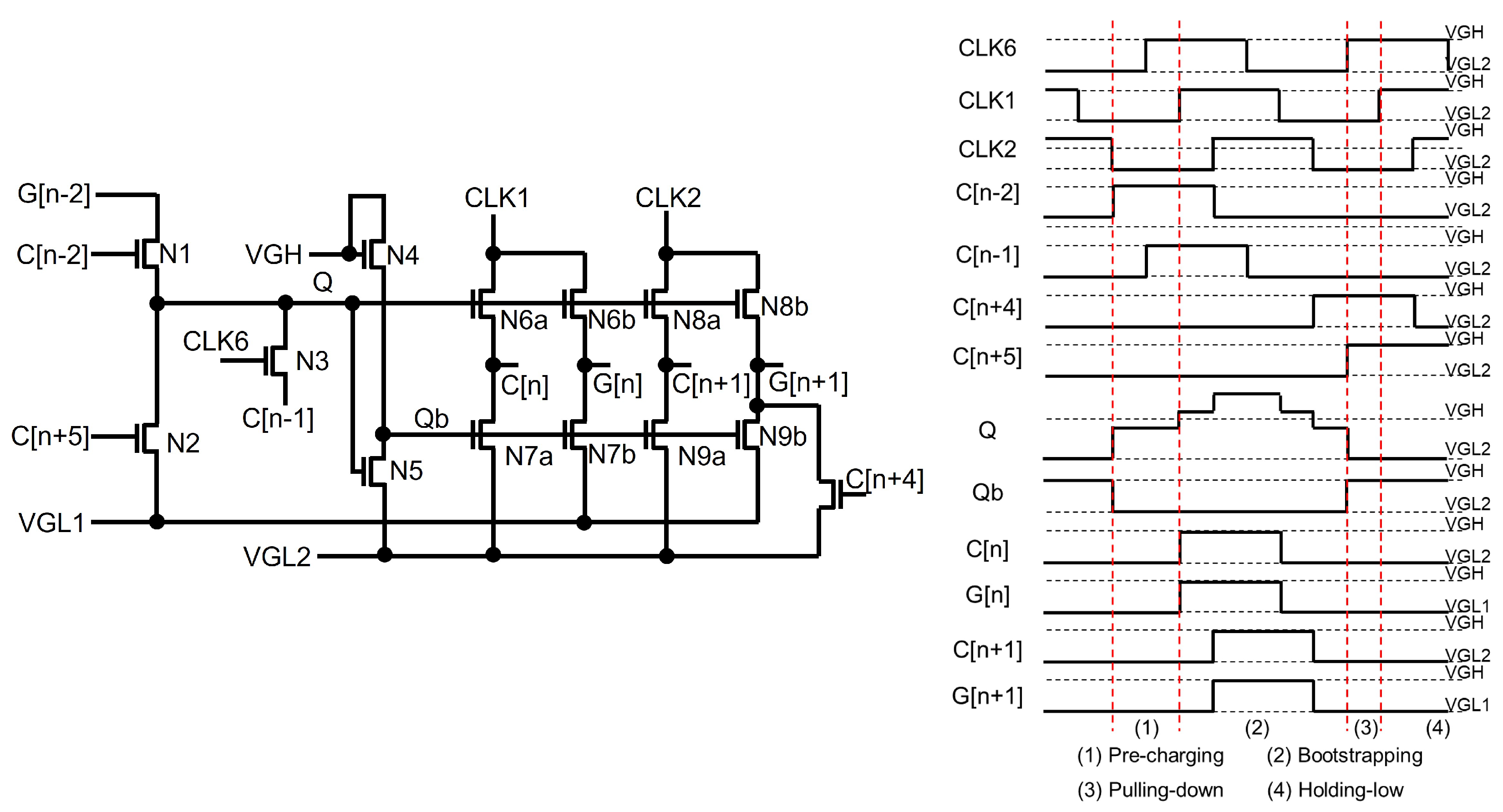
Figure 15.
Small area shift register with a Q-sharing structure by separating TFTs [92]
Figure 15.
Small area shift register with a Q-sharing structure by separating TFTs [92]
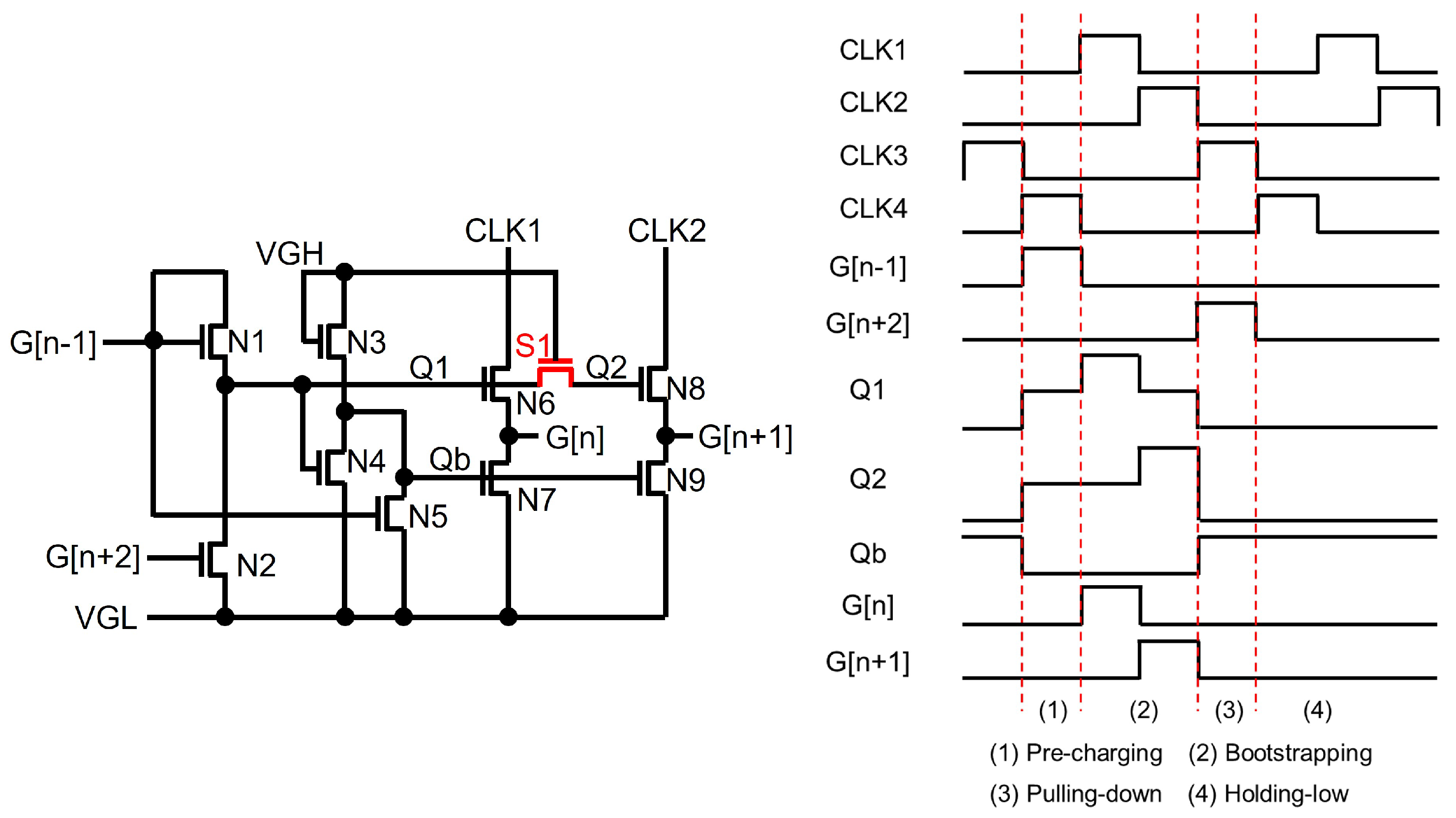
Figure 16.
Threshold voltage compensation pixel circuit example [107]
Figure 16.
Threshold voltage compensation pixel circuit example [107]
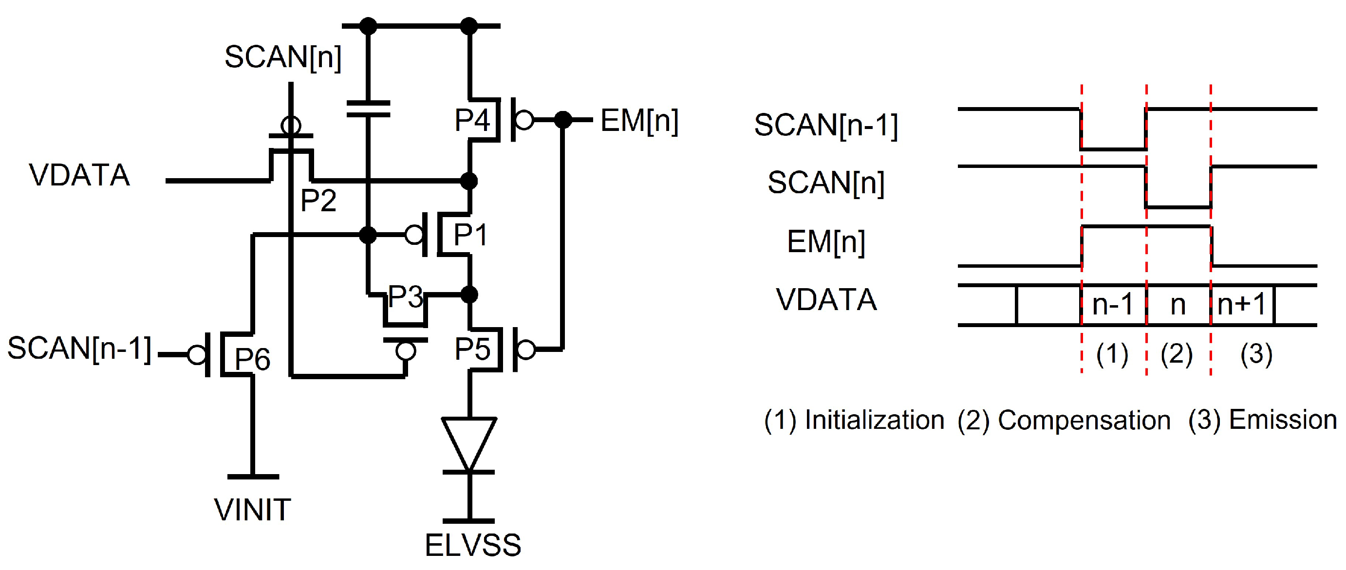
Figure 17.
Emission pulse generation circuit based on P-type TFTs [106]
Figure 17.
Emission pulse generation circuit based on P-type TFTs [106]
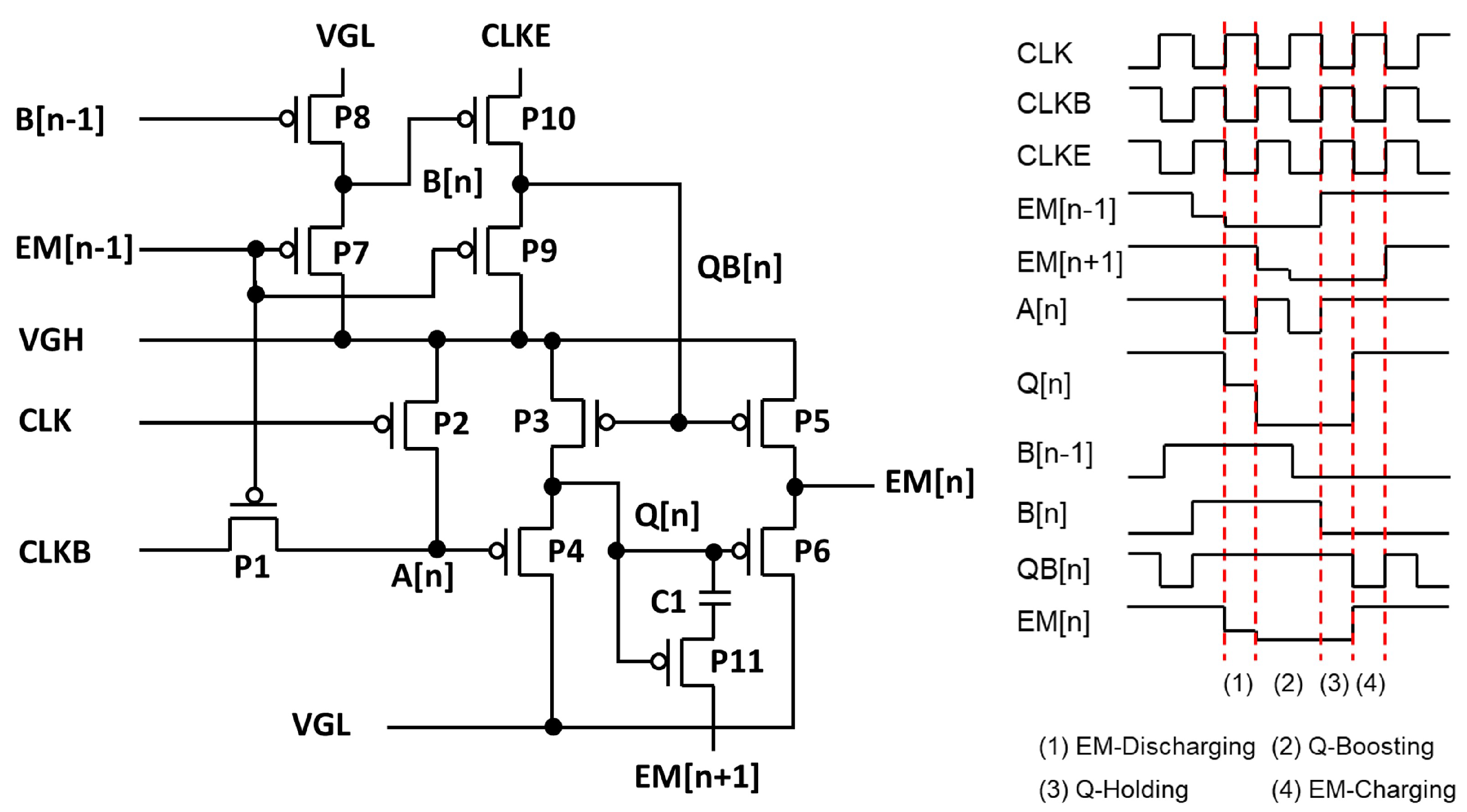
Figure 18.
Foveation-based driving schemes with the vertical resolution reduction [111]
Figure 18.
Foveation-based driving schemes with the vertical resolution reduction [111]
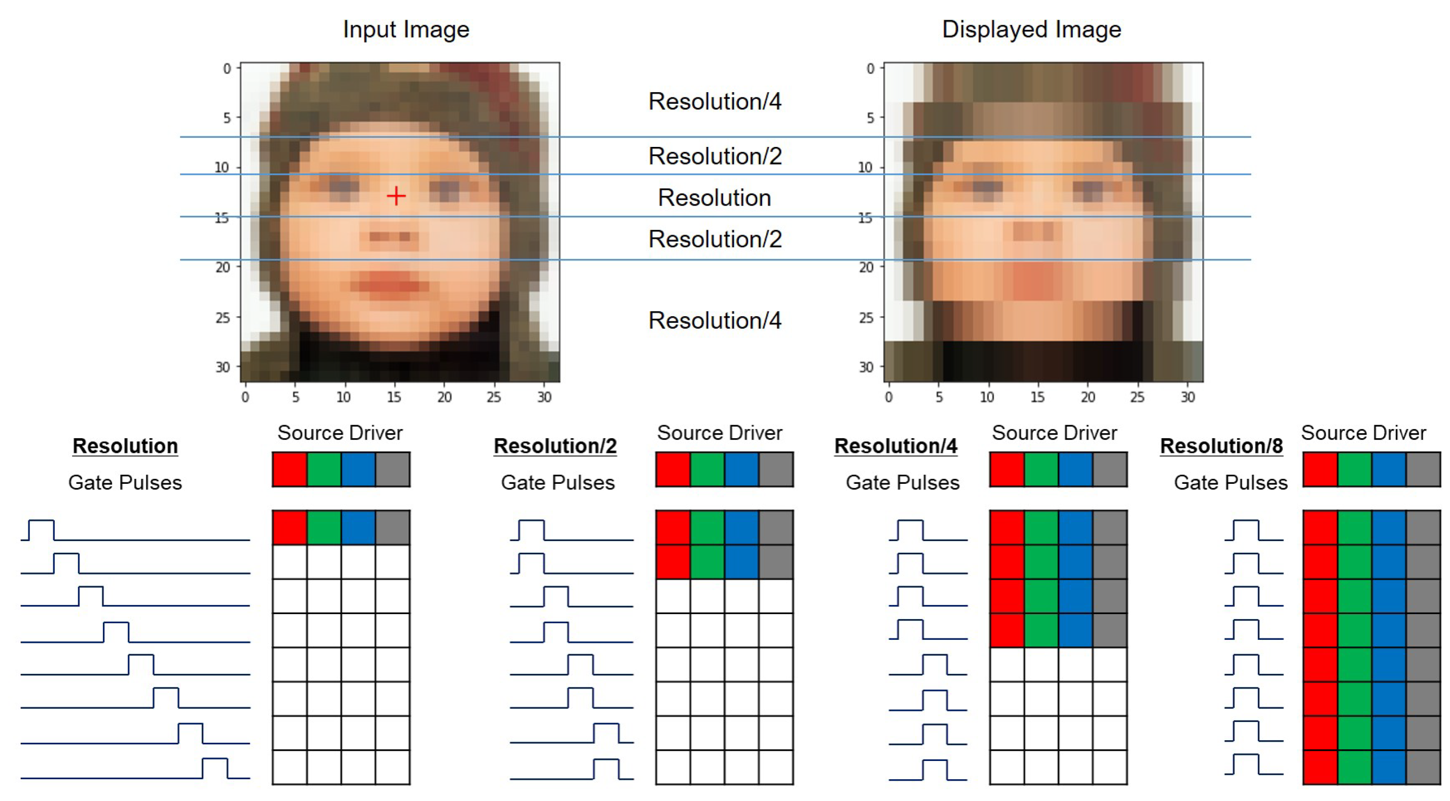
Figure 19.
Timing diagram of display scanning and touch sensing at TDDM [115]
Figure 19.
Timing diagram of display scanning and touch sensing at TDDM [115]
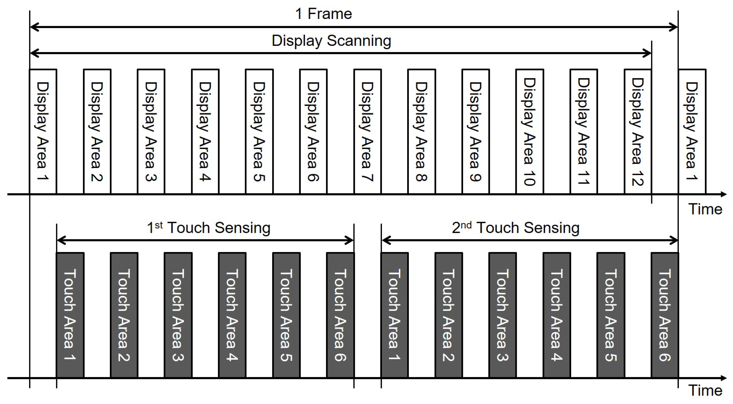
Figure 20.
Timing diagram of display scanning and touch sensing at TDDM [118]
Figure 20.
Timing diagram of display scanning and touch sensing at TDDM [118]
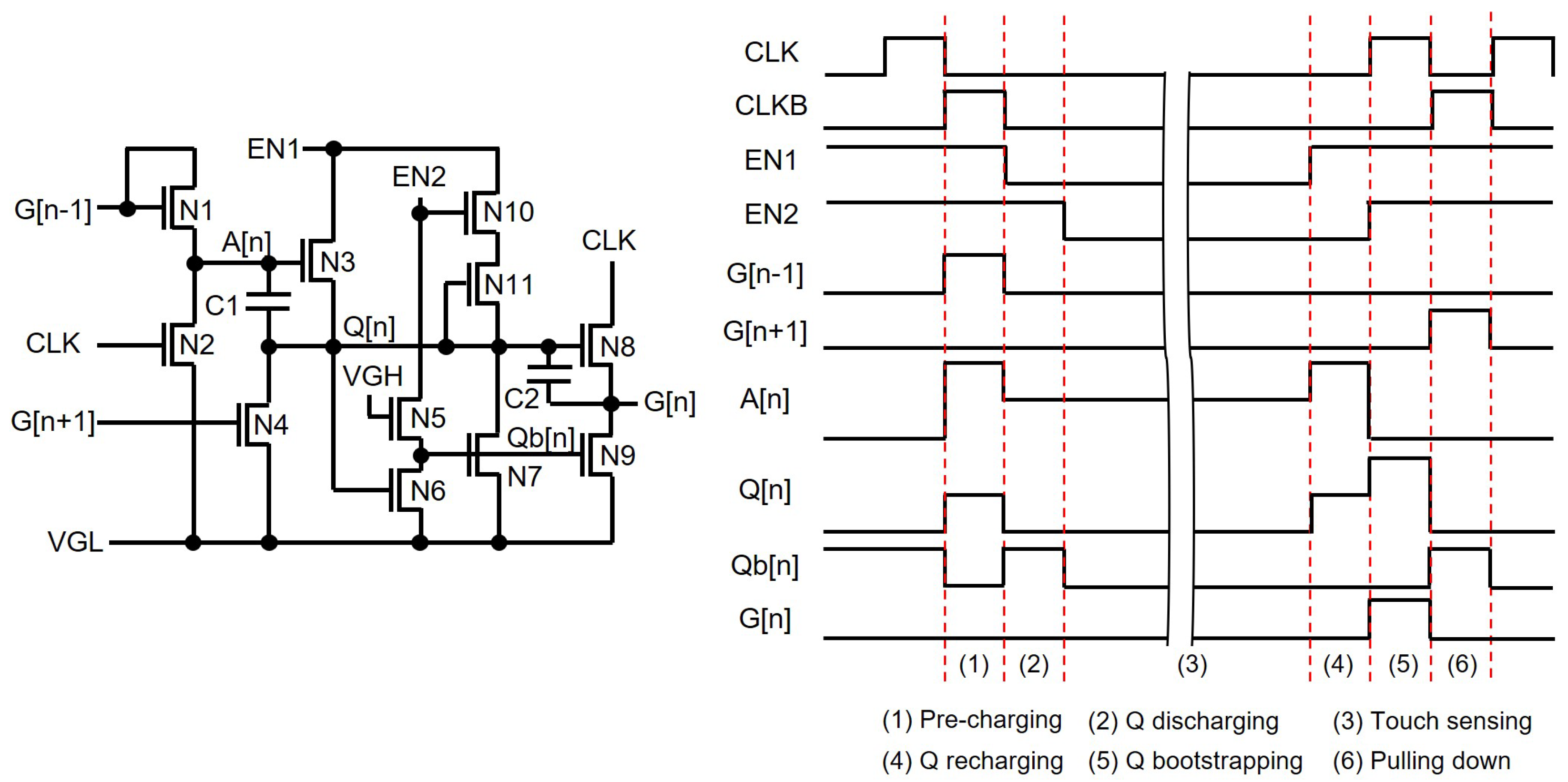
Figure 21.
Pixel circuit with a sensing TFT (N3) for the external compensation [128]
Figure 21.
Pixel circuit with a sensing TFT (N3) for the external compensation [128]
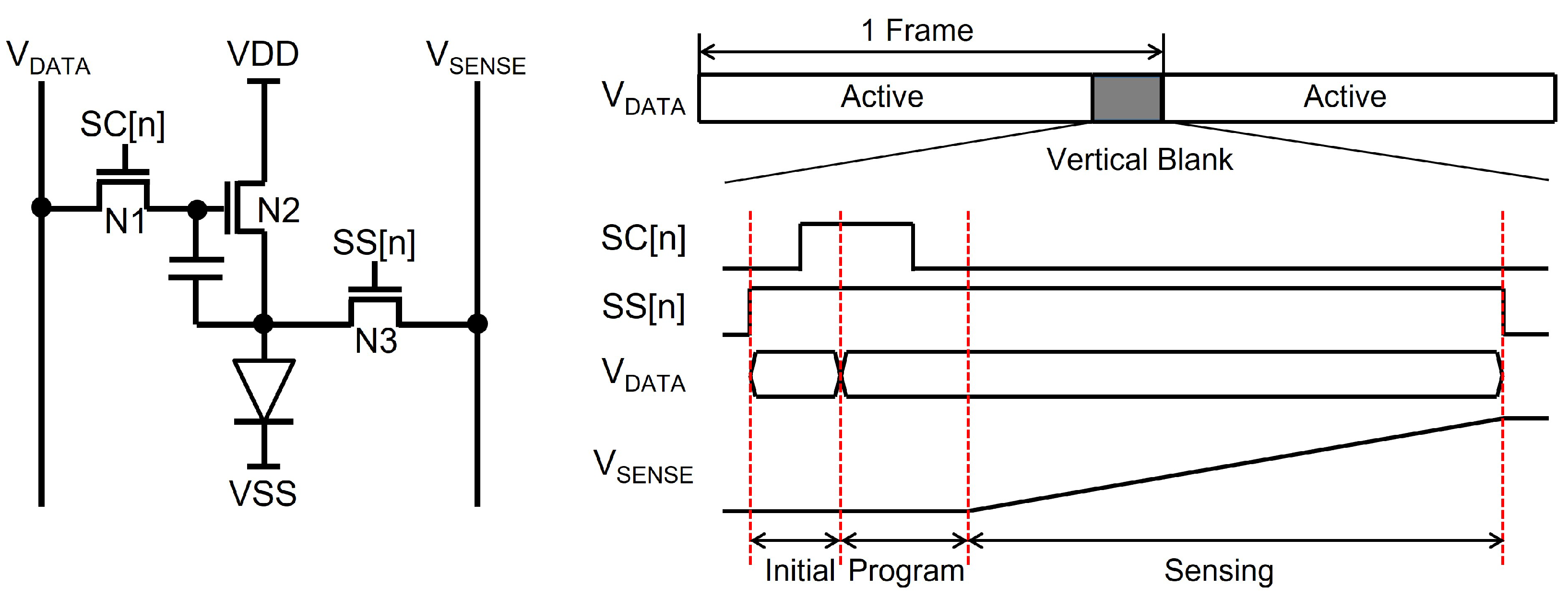
Figure 22.
Random sensing line selection during the vertical blank period [128]
Figure 22.
Random sensing line selection during the vertical blank period [128]
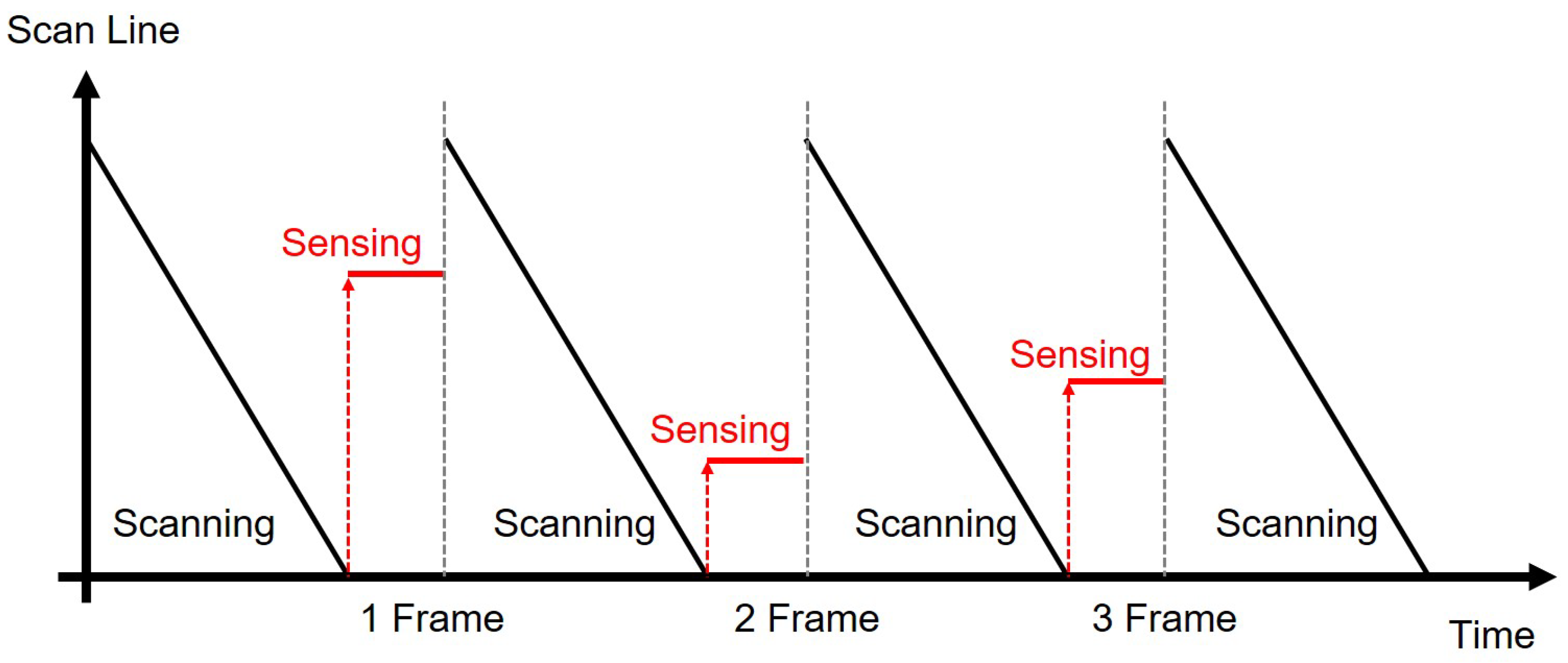
Figure 23.
Random sensing pulse generation. (a) Schematic (b) Timing diagram [128]
Figure 23.
Random sensing pulse generation. (a) Schematic (b) Timing diagram [128]
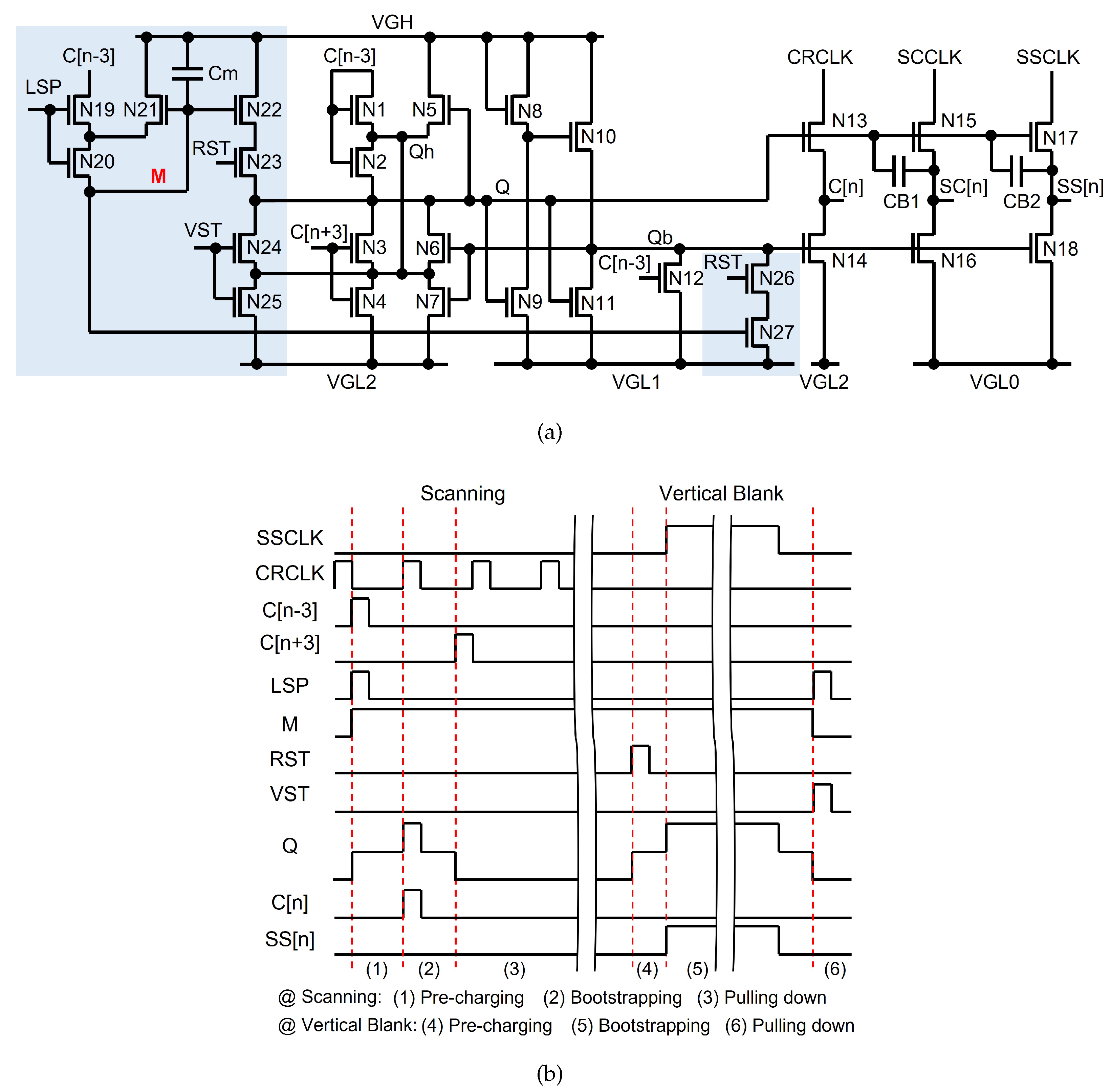
Figure 24.
Selective scan driver circuit to enable the gate pulse generation only for the specific region. [135]
Figure 24.
Selective scan driver circuit to enable the gate pulse generation only for the specific region. [135]
Disclaimer/Publisher’s Note: The statements, opinions and data contained in all publications are solely those of the individual author(s) and contributor(s) and not of MDPI and/or the editor(s). MDPI and/or the editor(s) disclaim responsibility for any injury to people or property resulting from any ideas, methods, instructions or products referred to in the content. |
© 2024 by the authors. Licensee MDPI, Basel, Switzerland. This article is an open access article distributed under the terms and conditions of the Creative Commons Attribution (CC BY) license (http://creativecommons.org/licenses/by/4.0/).
Copyright: This open access article is published under a Creative Commons CC BY 4.0 license, which permit the free download, distribution, and reuse, provided that the author and preprint are cited in any reuse.


