Submitted:
25 May 2024
Posted:
27 May 2024
You are already at the latest version
Abstract
Random variations in microelectronic circuit structures represent the source of entropy for physical unclonable functions (PUFs). In this paper, we investigate delay variations that occur through the routing network and switch matrices of a field programmable gate array (FPGA). The delay variations are isolated from other components of the programmable logic, e.g., Look-up tables (LUTs), flip-flops (FFs), etc. using a feature of Xilinx FPGAs called dynamic partial reconfiguration (DPR). A set of partial designs are created that fix the placement of a time-to-digital converter (TDC) and supporting infrastructure to enable the path delays through the target interconnect and switch matrices to be extracted by subtracting out common-mode delay components. Delay variations are analyzed in the different levels of routing resources available within FPGAs, i.e., local routing and across chip routing. Data is collected from a set of Xilinx Zynq 7010 devices, and a statistical analysis of within-die variations in delay through a set of the randomly-generated and hand-crafted interconnects is presented.
Keywords:
FPGA interconnect
; Delay variations
; Physical Unclonable Functions
1. Introduction
A physical unclonable function (PUF) is a hardware security primitive that is tasked with generating random bitstrings and encryption keys. The security properties of a PUF architecture are closely tied to the physical layer components that define its source of entropy, i.e., the layout characteristics of the circuit structure from which random variations are measured, digitized and processed into bitstrings. Although many different types of integrated circuits can by used as the platform for a PUF, the FPGA is a popular choice because it allows prototypes to be created and validated quickly while providing layout-level control over the design of the PUF’s circuit structures. Moreover, advanced FPGA features such as dynamic partial reconfiguration (DPR) can be leveraged to impede adversarial reverse engineering attacks, by making physical layer components of the PUF architecture unavailable in operational systems.
The physical layout components of a FPGA device consist of look-up tables (LUTs), flip-flops (FFs), switch matrices (SMs) and wires, plus sets of commonly used components including block RAMs, digital-signal-processing (DSP) blocks and digital clock managers (DCMs). The performance characteristics of these components are impacted by imperfections in the device manufacturing process. Processing variations affect each device differently, making, e.g., the propagation delay along the same routes in different chips distinct. The random and unique nature of process variation effects represent the cornerstone of PUF technology. This paper focuses on the analysis of variation in constituent elements of the FPGA, namely, the SMs and wires.
The experimental evaluation carried out in this work is performed on device instances of the Xilinx Zynq system-on-chip (SoC) 7010 architecture, which consists of a processor system (PS) and programmable logic (PL) region. The SMs in the PL component are responsible for configuring routes and for implementing fan out connections of input wires to multiple out-going wires. The implementation details of the SMs are not provided to end users because they are considered proprietary. However, low-level routing tools allow routes through SMs to be manipulated. In an initial set of experiments, called Hand-Crafted, we use routing commands to re-route signals through SMs as a means of extending a set of reference routes, called , to include additional wires and SMs, called . A second larger Tool-Crafted design is created in which the Vivado place&route tool is used to create the BaseRoutes and RouteExts, as an alternative to the hand-crafted routes of the first design.
The delay of the RouteExts are extracted and isolated by subtracting out the BaseRoute delay. DPR is used as a means of eliminating artifacts introduced by MUXs (LUTs) in the delays of the RouteExts by fixing all LUT positions in the DPR bitstreams to the same locations. The RouteExts in the hand-crafted design are constructed to include different types of routing resources, including single, double, quad and long lines. Delay measurements are made using an on-chip, high resolution timing engine, which provides a resolution of picoseconds (ps). Multiple sample averaging is used to increase resolution even further.
Delay measurements are carried out on the RouteExts instantiated on a set of identically configured Zynq 7010 devices, and a statistical analysis of delay variation is presented. Given our goal is to measure the contribution of SMs and routing wires to entropy leveraged by a delay-based PUF, only room temperature experiments are carried out. The following contributions characterize the technique and results presented in this paper.
- A dynamic partial reconfiguration technique is applied to measure and isolate the delays associated with wires and SMs in the programmable logic of a set of FPGAs.
- Wire and SM configurations are constructed using different routing resource types to assess the impact of wire length on the level of entropy.
- A series of data post-processing operations are proposed as a means of extracting only within-die delay variations, which represent the most robust random source of variations for a PUF.
- An estimate of within-die variations is derived for a wire-SM combination, and an analysis of the bitstrings derived using only wire-SM delay variations is presented to determine their statistical properties.
2. Background
In [1], the authors use dynamic reconfiguration to enable fine control over delays in experiments which use a time-to-digital converter (TDC) by manipulating route options through SMs. A fine resolution delay tuning method to improve linearity in TDCs is proposed in [2]. The authors introduce additional capacitive loads, as fan out branches, to nets passing through SMs.
A path delay timing method is proposed in [3] that constructs nearly identical path structures and uses differencing to obtain the delay of the changed segment. The goal of the work was to accurately measure the impact of extending paths using additional routing resources (similar to the work proposed here). However, dynamic partial reconfiguration was not used to create the path length extensions, resulting in additional artifacts introduced by changing pin locations in the static portion of the path. Moreover, the authors provide very little data on within-die and across-chip variations.
A RO-based differential delay characterization method is proposed in [4] for application to variation aware design (VAD) methodologies. Multiple ROs are constructed with overlapping path segment components and a set of equations are solved to deduce the path segment delays. A RO construction technique allowed statistical delay characterization of individual LUTs and direct, double and hex path segment delays.
Tuan et. al [5] investigate within-die variation in 65-nm FPGAs using a unique RO structure composed of non-inverting buffers and self-timed reset latches. The measured within-die variations are decomposed into random and systematic components. The analysis and techniques can be used to improve performance of devices using a location-aware timing model. More recently, the authors of [6] use soft-macro sensors to characterize within-die and die-to-die variation for creating device-signature variability maps. They too decompose variability into random and systematic components, and expand the analysis to include different FPGA resources and across temperature-voltage operating conditions.
The authors of [7] propose a finely tunable programmable delay line (PDL) mechanism with high precision and low overhead using a single LUT. A PDL-based symmetric switch method is applied to an arbiter-based PUF to correct delay discrepancies caused by FPGA routing asymmetries. By applying majority voting and categorization of challenges into reliability groups, they show that PUF response stability can be increased across adverse environmental conditions.
In [8], the authors utilize two distinct manual placement and routing approaches to enhance precision of FPGA-based TDCs. In the first approach, uniform routing paths and controlled delay elements are used while the second approach enhances the first by introducing a combination of long and short routing wires. Notably, the second approach achieved better dynamic range and resolution.
A comprehensive overview of how measurements can be conducted on FPGAs to characterize within-die delay variability is proposed in [9]. The authors propose precise measurement techniques to analyze both systematic and stochastic delay variability in FPGAs by employing an array of ring oscillators and critical path tests on various 90nm FPGA devices. This approach enabled them to quantify the variability and analyze its impact on future FPGA technologies.
A Programmable Ring Oscillator PUF (PRO PUF) is introduced in [10], which utilizes dynamic partial reconfiguration to generate bitstrings by manipulating switch matrices within its architecture. The architecture is divided into static and dynamic areas, with the latter being modifiable during operation, specifically altering signal transmission paths in the switch matrix without affecting other structural components. Bitstring generation and the selection of different transmission paths through the switch matrix are controlled by challenge, with each unique path corresponding to a specific external configuration file, enabling the generation of a wide array of challenge response pairs (CRPs).
The technique proposed in this paper shares similarities with [10], particularly as it relates to the application of DPR and the utilization of static and dynamic regions. However, the approach proposed in [10] explores routing networks within the DPR region but does not explicitly remove variations introduced by the LUT architecture. Additionally, rather than using a challenge to specify each configuration, our approach applies only two partial bitstreams, which fix the LUT positions in both designs. The delays measured using the BaseRoute and RouteExt partial bitstreams enables, through differencing, only variations introduced by the routing wires and switch matrices to contribute to the entropy of generated bitstrings.
3. System Architecture
A block diagram showing the system architecture implemented on the Xilinx Zynq 7010 device is given in Figure 1. The PL component shown along the top consists of two regions; a static region (SR) on the left and a dynamic partial reconfiguration (DPR) region on the right. The SR region incorporates a set of state machines and a time-to-digital converter (TDC), as well as a register interface, labeled GPIO for general purpose input/output, to the processor system component of the SoC. The Controller and TDC are capable of measuring path delays at a resolution of ps in single-shot mode, and up to a total path length of nanoseconds [11]. In our experiments, the paths are measured 16 times and averaged to reduce measurement noise in the single-shot measurements.
Two experimental designs are evaluated in this paper. In both designs, a set of BaseRoutes and RouteExts are created. The implementation layouts of the BaseRoute and RouteExts are identical everywhere except for the wires and SMs used for the route(s) between the source and destination LUTs. The BaseRoutes and RouteExts in first design are hand-crafted to allow a wide variety of routing resources to be utilized in the RouteExt designs, e.g., single, double, quad and long lines. The BaseRoutes and RouteExts are implemented in a set of 67 partial bitstreams, one-at-a-time. The second design utilizes only one BaseRoute DPR region and one RouteExt DPR region, and includes a set of 8192 distinct paths, composed of series-connected RouteExts, that can be configured and tested using an input challenge. The first design is referred to as Hand-Crafted, while the second one is referred to as Tool-Crafted.
As an example, the right side of Figure 1 shows the DPR regions for the BaseRoute (top) and RouteExt (bottom) from a Hand-Crafted experiment. P&R constraints are used in the Xilinx Vivado CAD tool flow to construct both implementations, which fix the positions of the wires, SMs and LUTs. The regions enclosed by the rectangles show routing components that are locked down and remain static in both DPR bitstreams. The route is modified only in the region circled on the right. The base route passes directly through the SM while the route extension extends the route to other wire and SM components.
The testing process first programs the DPR region with the BaseRoute DPR bitstream and measures the delay. The FPGA is then reprogrammed with the RouteExt DPR bitstream and the path is re-measured. The delay of the wires and SMs that define the route extension is obtained by subtracting the BaseRoute delay from the RouteExt delay, which removes all common-mode components of the path delay. In many cases, the RouteExt design from the previous experiment is used as the BaseRoute for the next design, extending the route further in successive experiments.
The second, tool-generated, design utilizes two stacked modules from the SiRF PUF called the reconvergent-fanout module (RFM) [12]. A block diagram of the RFM is shown in Figure 2. The module consists of two rows of 4-to-1 MUXs separated by AND, OR and AND-OR (AO) gates (the experimental design inserts two more rows identical to those shown). The select inputs to the MUXs are controlled by the row-path-select (RPS) inputs on the left. The same gate configuration is repeated across four columns, through , with the logic gate outputs distributed across all four columns using rotate input and output, and , wires. Rising and falling transitions are introduced by a Launch FF shown along the top of the figure, which fans-out to the logic gate inputs in each of columns. A 16-to-1 MUX, shown along the bottom of the figure, is used to select a path to be timed by the TDC. The design with two stacked RFM modules possesses 131,072 distinct paths, of which 8192 are testable with rising and falling transitions using 132-bit challenges.
Unlike the Hand-Crafted design, placement constraints are used only to fix the placement of the LUTs implementing the logic gates and MUXs, and the Vivado P&R tool is used to create the routing structure. In order to force the P&R tool to create different routes in the BaseRoute and RouteExt designs, a timing constraint is used during the implementation of the BaseRoute which is removed during the implementation of the RouteExt. The 13 ns timing constraint forces the P&R tool to construct a routing architecture that minimizes the number of wires and series-inserted SMs between the fixed LUT inputs and outputs. The LUT input/output nets in the RouteExt design, on the other hand, almost always utilize a larger number of wires and SMs, resulting in longer delays. The Vivado implementation views in Figure 3 show the static design of the SiRF PUF timing engine and bitstring generation algorithm on the right and BaseRoute and RouteExt DPR regions on the left.
3.1. FPGA Tool Flow
A flowchart of the bitstream generation process is depicted in Figure 4. The operations carried out in the five step process are as follows.
- Synthesize the timing engine and other components of the static design.
- Routing constraints are used to fix SMs and wires for the Hand-Crafted experiment in 67 separate designs, while timing constraints are used to force different routes from the Vivado PNR tool in the Tool-Crafted experiment.
- TCL commands are used to create the DPR region, which is represented as a pblock in Vivado. The locked static design is used to maintain the exact same layout in all DPR designs created.
- PNR is run to join the static and DPR designs.
- The full bitstream is used to program the device, followed by any sequence of partial bitstreams created by this tool flow.
3.2. Delay Post-Processing Algorithm
The data collected from the Hand-Crafted design is used to estimate the level of within-die variations (entropy) introduced by routing wires and SMs. The data post-processing algorithm is crafted to achieve this goal and is described in this section using timing data from a set of 34 Zynq 7010 FPGAs. The algorithm consists of four steps, and is illustrated in Figure 5.
- The programmable logic of the FPGAs is programmed with the full bitstream, followed by a sequence of partial bitstream programming operations. The timing engine measures both rising and falling delays of paths implemented within each of the partial bitstreams. The curves labeled 1) BaseRoute & RouteExt Raw Delay in Figure 5 show the rising path delays for the base route (black) and route extensions (blue) measured from the 34 FPGAs (falling delays are omitted). The acyonyms BR and RE refer to BaseRoute and RouteExtensions, respectively. We use the term Raw to refer to both sets.
- The RE and BR delays are calibrated to remove global process variations using a Global Process and Environmental Variation (GPEV) module. The GPEV module applies a pair of linear transformations given by Eqs. 1 through 4. The mean and standard deviation of the 134 Raw delays from each FPGA are computed and the Raw delays are standardized using Eqs. 1 and 3. A second linear transformation using 0.0 and 44.1 for , and (Eq. 4) is then applied to convert the standardized values back to a form similar to the original data (44.1 is the mean across all FPGAs). The same and are used for all devices in the second transformation, which effectively removes global performance differences while preserving within-die variations. Although difficult to observe, the variations in the rising delays across all FPGAs in the plot labeled 2) Compensate Raw Delays from Figure 5 are smaller than those from Step 1. We use the symbol ’F’ for FPGA, ’i’ for FPGA instance, ’c’ for calibrated and ’r’ for route in these equations. The GPEV calibrated delays are referred to as and .
- The rising and falling path delays from the BaseRoute design are subtracted from the corresponding rising and falling path delays of the RouteExt designs in the graph labeled 3) Subtract BaseRoute delay of Figure 5. We refer to these delay differences as and (DV is an acronym for delay value). The delays of the and vary from 80 picoseconds (ps) to 1.8 nanoseconds (ns) across all 67 rise and fall delays.
- The final transformation is shown in 4) Remove DC bias. The and posses a DC bias that exists because the routes are not identically designed. The process of removing bias is accomplished by computing the mean delay of each and across all FPGAs and then subtracting this offset from the compensated raw delays. We use the symbol ’R’ here to refer to individual route extensions and ’x’ for the route extension number. Eq. 5 and 6 gives expressions for computing the rise and fall compensated raw delays without bias, annotated as , with ’o’ referring to ’offset’.
3.3. Tool-Crafted Data Post-Processing
The goal in this Tool-Crafted experiment is to evaluate entropy and uniqueness-related statistics of bitstrings generated using the delays of only wire and SB components in the FPGAs. The sequence of graphs in Figure 6 show the data post-processing algorithm applied to the delays collected from one FPGA in this experiment. The data post-processing algorithm is modified with two additional steps over the process given for the Hand-Crafted experiments. Moreover, the addition of a differencing step to create DVD changes the step in which GPEV is applied.
- The Raw DVR and DVF are plotted in the upper left graph, where we show the first 100 rising delays on the left and the first 100 falling delays on the right, both from the larger sets of 4096 values in each group. The vertical shift in the two data sets, with rising delays having smaller overall delays, illustrates a common process-related characteristic that p-channel (pull-up) devices are not well correlated with n-channel (pull-down) devices on the same FPGA. This pattern varies depending on the FPGA.
- In contrast to the Hand-Crafted algorithm, the second step involves subtracting the BaseRoute delays from the RouteExt delays. The first 100 DVR and DVF are plotted in the 2) DVR and DVF graph.
- In step 3, the 4096 DVR are randomly paired and subtracted from the 4096 DVF, as a means of doubling the level of entropy in the delay differences (DVD). Note that additional DVD can be created by other random pairing and differencing operations applied to the DVR and DVF groups, up to a total of unique combinations.
- The operation carried out in Step 6 is optional, and serves only to make the number of strong bits in the generated bitstrings approximately the same for each FPGA when a threshold is applied (described below). The scaling operation computes the average range of the variation in the of each FPGA i and multiplies all by a ratio that makes the ranges approximately equal for all devices. The ratios vary between 1.00 and 1.91 and illustrate that the level of random variations (entropy) in each FPGA is not constant. We refer to the delays shown in Step 6 as (’S’ for scaled) in the following.
3.4. Bitstring Generation Algorithm
The data shown in Step 6 of Figure 6 is used as input to the bitstring generation algorithm. As indicated earlier, the GPEV transformation applied in Step 4 calibrates for chip-to-chip (global) process variations and delay variations introduced by adverse environmental conditions. The transformations carried out in Steps 5 and 6 remove DC bias and scale the remaining within-die variations of each device to make them similar across chips. All of these transformations are designed to make it possible to apply a simple bit-flip avoidance algorithm during bitstring generation that leverages the within-die random variations that remain, and produces bitstrings nearly equivalent in size.
Bitstring generation is the final step (Step 7) of the proposed data post-processing algorithm, and is illustrated in Figure 7 using the first 15 from the Tool-Crafted experiment. Here, the data for all 34 devices is superimposed, with the delays for only the first two device line-connected, and highlighted in red and blue, to illustrate the randomized behavior of the points above and below zero. The black points are associated with the remaining 32 devices. The y-axis is given in units returned by the TDC, where each unit value is equal to 18 ps of delay. The range of corresponds to ps.
The two horizontal lines represent thresholds that are used to improve reliability, i.e., points within the region between the threshold are not used during bitstring generation [12]. Given the focus of this paper is on the analysis of entropy within the constituent components of paths in FPGAs, we utilize room temperature only to analyze entropy and evaluate uniqueness in the generated bitstrings. Moreover, the bitstrings are generated using only those points above and below the thresholds, called strong bits, as a means of emulating the actual bitstring generation algorithm. Points above the upper threshold are assigned a bit value of 1, while those below the lower threshold are assigned 0.
4. Experimental Results
The experimental results for the Hand-Crafted and Tool-Crafted designs are presented separately in the following sections. As indicated, the analysis for the Hand-Crafted experiment is focused on determining the level of entropy that wires and SMs provide for delay-based PUFs implemented on FPGAs. The entropy contribution introduced by a third constituent element of FPGAs, namely, LUTs, as presented in [13], is discussed for completeness. The analysis presented for the Tool-Crafted experiments is focused on entropy and uniqueness statistical characteristics of bitstrings generated using wires and SMs as the only source of entropy.
4.1. Experimental Results: Hand-Crafted Design
The vertical range of the delays plotted for each Route # in the 4) Remove DC bias graph of Figure 5 portrays within-die variations for each of the hand-crafted routes. In our analysis, we correlate the width of the vertical ranges, measured as delay variations, with the physical layout characteristics of the routes. In particular, the number unit-sized wires and SMs are tabulated for each route as the metric proposed for the physical characteristics. The number of unit-sized wires is the number of equivalent single wires that define the route. In particular, double wires count as 2 single wires, quad wires count as 4, while long wires count as 6.
The number of unit-sized wires and SMs are plotted in Figure 8 as a stacked bar graph with the number of SMs shown along the bottom of each bar and the number of unit-sized wires shown along the top. Two degenerate cases occur for routes 14 and 66, where the changes between the BaseRoute and RouteExt involve only ’bounces’ within a single switch box, i.e., the remaining components of the route are identical. For route 14, multiple bounces in the RouteExt replace a single bounce in the BaseRoute, while for route 66, a single bounce replaces a different single bounce in the same SM. Figure 9 shows Vivado implementation views for the BaseRoute and RouteExt SM within the route 66 designs.
The scatter plot shown in Figure 10 plots the proposed physical characterization metric of the routes along the x-axis against the measured delay variations along the y-axis. The relationship between unit-size wires and SBs is factored in by adding a constant of 14.2 to the values in the bar graph for the number of unit-sized wires. The red points correspond to the rising delay variations while the blue points correspond to the falling delay variations. A linear regression analysis is performed on each group of points separately in support of determining the relationship between levels of entropy and physical characteristics of the wires and SMs. A least-squares estimate (LSE) of the regression line is plotted through both groups of points.
The LSE of the regression line is computed using a python function from the linear algebra library call lstsq. The numerical values from the bar graph in Figure 8, namely the number of unit-size wires and SMs, are used as our model and serve as input to this function. The function returns two coefficients and a y-intercept, with the former two values representing the weighted contribution of the wires and SMs, respectively, to the total measured entropy of the route.
The coefficients generated for the rising delays are 2.06 and 27.75 for wires and SMs, respectively, while those for the falling delays are 2.17 and 12.35. Here, we see the main contribution to entropy is due to the SMs, and the contribution by SMs is more than double for rising delays than it is for falling delays. Moreover, the close matching of the magnitudes for the wire coefficients support that fact that wire variation should be independent of a rising or falling transition. Last, the fact that both regression lines are nearly superimposed supports our modeling of the variation as two constituent components of the measured variations.
The value at in Figure 10 is approximately on average, and represents the delay variation introduced by a single wire-SM combination. For comparison, the result presented in [13] indicates that the (range) of delay variation associated with the LUT in Zynq 7010 FPGAs is approximately 30 ps. Therefore, the variation introduced by a wire-SM combination is somewhat smaller than the variation introduced by a LUT.
4.2. Experimental Results: Tool-Crafted Design
The delays measured in the Tool-Crafted experiments is used to generate 128-bit bitstrings for each of the 34 FPGAs. The bitstrings are subjected to several statistical tests including inter-chip hamming distance (HD), NIST statistical tests, entropy and min-entropy tests to evaluate their statistical quality.
Inter-chip hamming distance measures the uniqueness of the bitstrings by counting the number of bits that are different in pairings of the bitstrings from different chips. The ideal value is 50%, which indicates that half of the bits are different in each pairing. Eq. 7 is used to compute inter-chip hamming distance, with and representing the size of the bitstrings from FPGAs i and j. The number of bits compared is given by k, which is a subset of the bits in both bitstrings of the pair. Only strong bits corresponding to the same within the two bitstrings of the pair are considered in the HD calculation, which is given by k. The distribution of the inter-chip HDs is shown in Figure 11. The distribution varies from approximately 43% to 56% and possesses a mean value close to ideal at 50.04%.
The results of the NIST statistical tests applied to the bitstrings of length 128 bits is shown in Figure 12. Only six of the NIST tests are applicable given the limited size of the bitstrings. All tests are passed with 34 FPGAs passing 5 of the tests and with 33 FPGAs passing the Runs test. The entropy and min-entropy of the bitstrings is computed as 0.9957 and 0.9084, respectively. These results indicate the bitstrings are of cryptographic quality.
5. Conclusions
An analysis of within-die variations (entropy) in the constituent elements of an FPGA, namely, wires and switch matrices, is presented in this paper. Within-die variations of these components is isolated by using a feature of FPGAs called dynamic partial reconfiguration (DPR) and a set of constraints. The constraints are used to fix the locations of LUTs and components of the timing engine. Partial bitstreams are created which vary the routing characteristics of two versions of the design, one which instantiates a set of base routes (called the BaseRoute design ) and a second which extends the base routes by adding wires and additional switch matrices, called the RouteExt design.
The LUTs are fixed to the exact same positions in both designs, allowing components of the path delays related only to the route extensions to be isolated through a delay difference operation. We analyze the RouteExt delays from two sets of experiments, one designed to allow variations in the constituent elements of the path to be analyzed, called Hand-Crafted, and a second designed to allow an analysis of the statistical properties of the bitstrings generated using only entropy contributed by wires and SMs, called Tool-Crafted.
The results show the within-die variations in delay associated with a SM is approximately 17 ps, in contrast, the delay variations of a LUT, as reported in previous work, is approximately 30 ps. This enables paths for PUF applications to be constructed with levels of entropy that meet target goals.
The results show that the statistical characteristics of the bitstrings generated in the Tool-Crafted experiments are of high quality, achieving nearly 50% for inter-chip hamming distance (the ideal value) and passing all applicable NIST statistical tests.
Future work will investigate path construction techniques that optimize entropy by creating a diverse netlist of SMs, wires and LUTs. PUF architectures constructed in this fashion will be more robust to adverse environmental conditions and machine learning attacks.
Author Contributions
All authors contributed to the study conception and design. Material preparation, data collection and analysis were performed by Jenilee Jao and Jim Plusquellic. The first draft of the manuscript was written by Jenilee Jao, Jim Plusquellic, Ian Wilcox, Biliana S Paskaleva and Pavel B Bochev and all authors commented on previous versions of the manuscript. All authors read and approved the final manuscript.
Funding
Supported in part by the Laboratory Directed Research and Development program at Sandia National Laboratories, a multimission laboratory managed and operated by National Technology and Engineering Solutions of Sandia, LLC., a wholly owned subsidiary of Honeywell International, Inc., for the U.S. Department of Energy’s National Nuclear Security Administration under contract DE-NA-0003525.
Institutional Review Board Statement
Not applicable
Informed Consent Statement
Not applicable
Data Availability Statement
Dataset available on request from the authors
Acknowledgments
This paper describes objective technical results and analysis. Any subjective views or opinions that might be expressed in the paper do not necessarily represent the views of the U.S. Department of Energy or the United States Government.
Conflicts of Interest
The authors have no relevant financial or non-financial interests to disclose.
References
- Bergeron, E.; Feeley, M.; Daigneault, M.A.; David, J.P. Using dynamic reconfiguration to implement high-resolution programmable delays on an FPGA. In Proceedings of the 2008 Joint 6th International IEEE Northeast Workshop on Circuits and Systems and TAISA Conference; 2008; pp. 265–268. [Google Scholar] [CrossRef]
- Berrima, S.; Blaquière, Y.; Savaria, Y. Fine resolution delay tuning method to improve the linearity of an unbalanced time-to-digital converter on a Xilinx FPGA. IET Circuits, Devices & Systems 2020, 14, 1243–1252. [Google Scholar] [CrossRef]
- Ruffoni, M.; Bogliolo, A. Direct Measures of Path Delays on Commercial FPGA Chips. In Proceedings of the Proceedings: 6th IEEE Workshop on Signal Propagation on Interconnects; 2002; pp. 157–159. [Google Scholar] [CrossRef]
- Yu, H.; Xu, Q.; Leong, P.H. Fine-grained characterization of process variation in FPGAs. In Proceedings of the 2010 International Conference on Field-Programmable Technology; 2010; pp. 138–145. [Google Scholar] [CrossRef]
- Tuan, T.; Lesea, A.; Kingsley, C.; Trimberger, S. Analysis of within-die process variation in 65nm FPGAs. In Proceedings of the 2011 12th International Symposium on Quality Electronic Design; 2011; pp. 1–5. [Google Scholar] [CrossRef]
- Taka, E.; Maragos, K.; Lentaris, G.; Soudris, D. Process Variability Analysis in Interconnect, Logic, and Arithmetic Blocks of 16-Nm FinFET FPGAs. ACM Trans. Reconfigurable Technol. Syst. 2021, 14. [Google Scholar] [CrossRef]
- Majzoobi, M.; Kharaya, A.; Koushanfar, F.; Devadas, S. Automated Design, Implementation, and Evaluation of Arbiter-based PUF on FPGA using Programmable Delay Lines. IACR Cryptol. ePrint Arch. 2014, 2014, 639. [Google Scholar]
- Siecha, R.T.; Alemu, G.; Prinzie, J.; Leroux, P. 5.7 ps Resolution Time-to-Digital Converter Implementation Using Routing Path Delays. Electronics 2023, 12. [Google Scholar] [CrossRef]
- Sedcole, P. ; K. Cheung, P.Y. Within-die delay variability in 90nm FPGAs and beyond, Proceedings of the 2006 IEEE International Conference on Field Programmable Technology; 2006; pp. 97–104. [Google Scholar] [CrossRef]
- Cui, Y.; Chen, Y.; Wang, C.; Gu, C.; O’Neill, M.; Liu, W. Programmable Ring Oscillator PUF Based on Switch Matrix. In Proceedings of the 2020 IEEE International Symposium on Circuits and Systems (ISCAS); 2020; pp. 1–4. [Google Scholar] [CrossRef]
- Owen Jr., D.; Heeger, D.; Chan, C.; Che, W.; Saqib, F.; Areno, M.; Plusquellic, J. An Autonomous, Self-Authenticating, and Self-Contained Secure Boot Process for Field-Programmable Gate Arrays. Cryptography 2018, 2. [Google Scholar] [CrossRef]
- Plusquellic, J. Shift Register, Reconvergent-Fanout (SiRF) PUF Implementation on an FPGA. Cryptography 2022, 6. [Google Scholar] [CrossRef]
- Jao, J.; Wilcox, I.; Thotakura, S.; Chan, C.; Plusquellic, J.; Paskaleva, B.S.; Bochev, P.B. An Analysis of FPGA LUT Bias and Entropy for Physical Unclonable Functions. Journal of Hardware and Systems Security 2023. [Google Scholar] [CrossRef]
Figure 1.
Block diagram of the test architecture for the Hand-Crafted experiments showing the Programmable Logic and Processor System partitions on a Xilinx Zynq 7010 SoC. The static region is shown on the left, which includes the path delay timing engine. Two dynamic partial reconfiguration instances of the routing architecture are shown on the right.
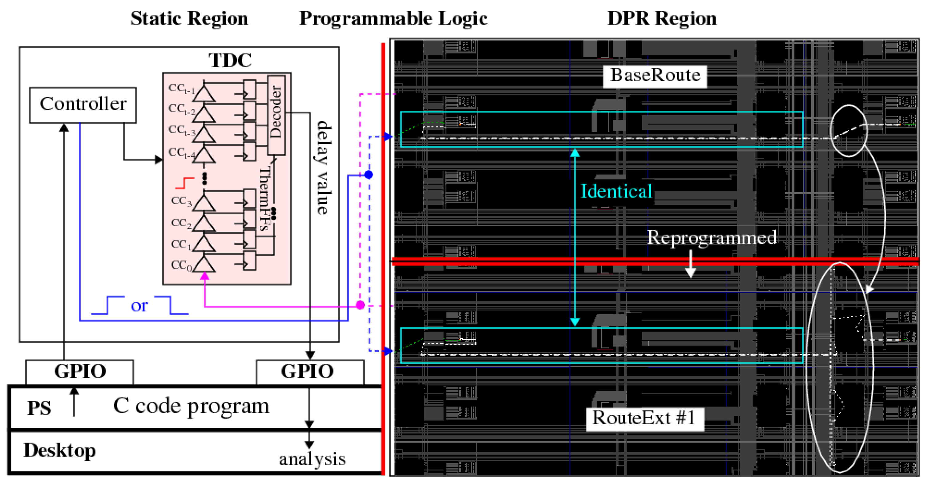
Figure 2.
Block diagram of the reconvergent-fanout module (RFM).
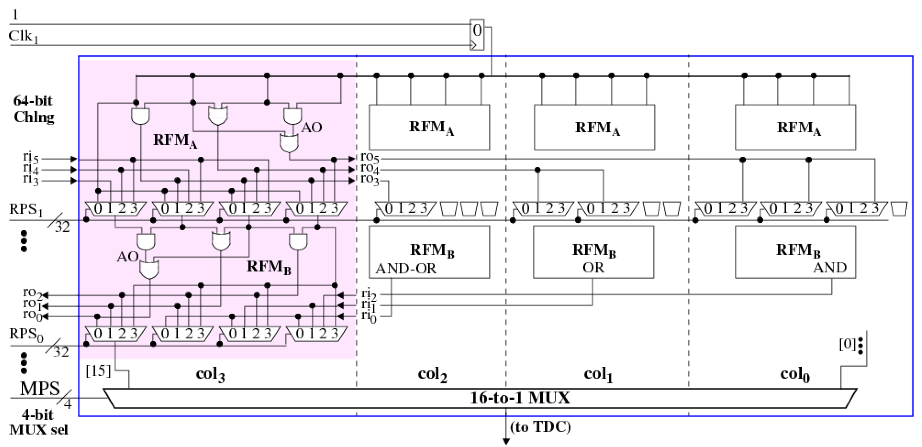
Figure 3.
Tool-Crafted Experiment: Implementation views of the static portion (left), and BaseRoute and RouteExt DPR regions (right).
Figure 3.
Tool-Crafted Experiment: Implementation views of the static portion (left), and BaseRoute and RouteExt DPR regions (right).
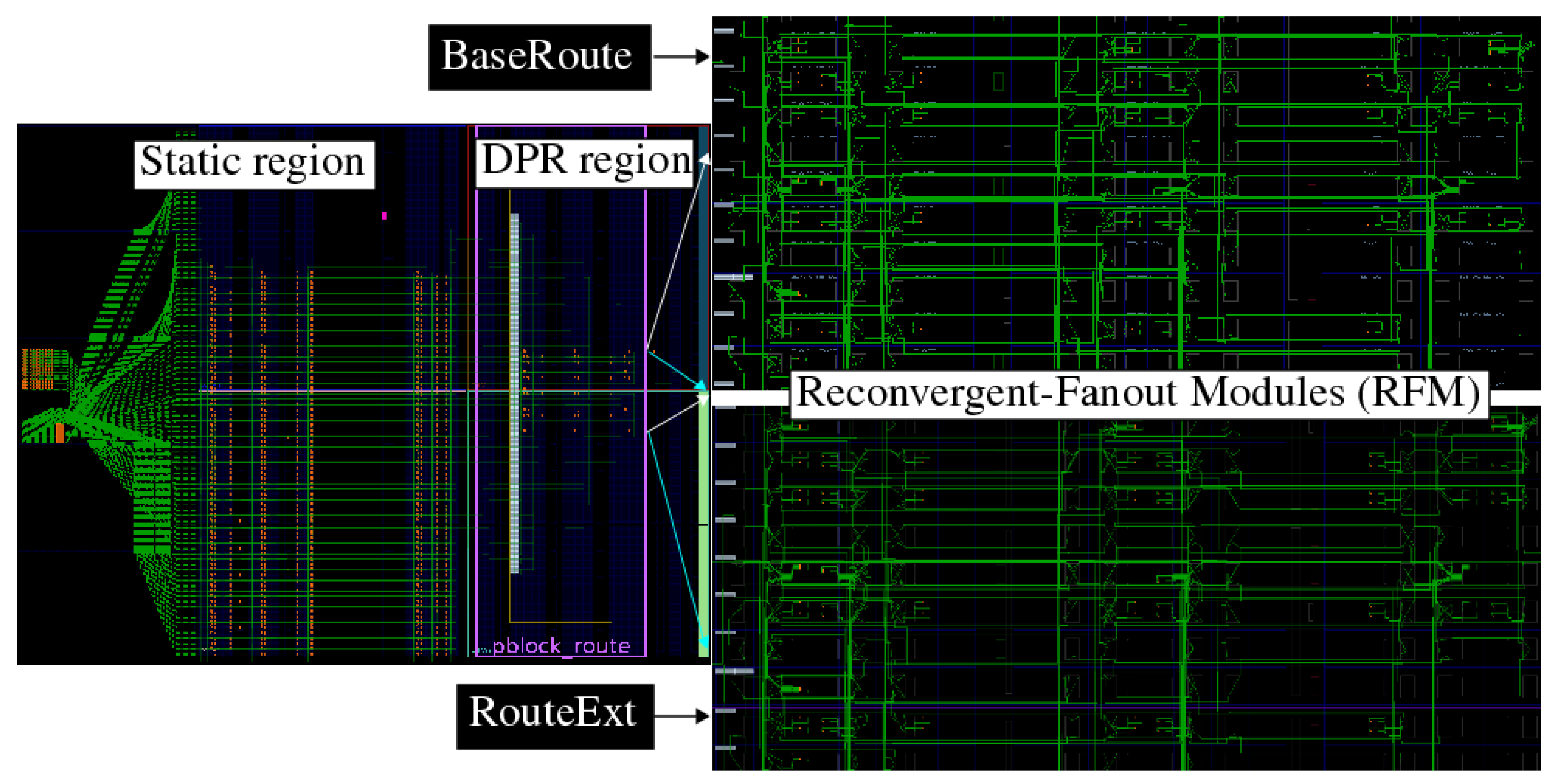
Figure 4.
Xilinx Vivado tool flow for generating full and partial bitstreams for Hand-Crafted and Tool-Crafted experiments.
Figure 4.
Xilinx Vivado tool flow for generating full and partial bitstreams for Hand-Crafted and Tool-Crafted experiments.
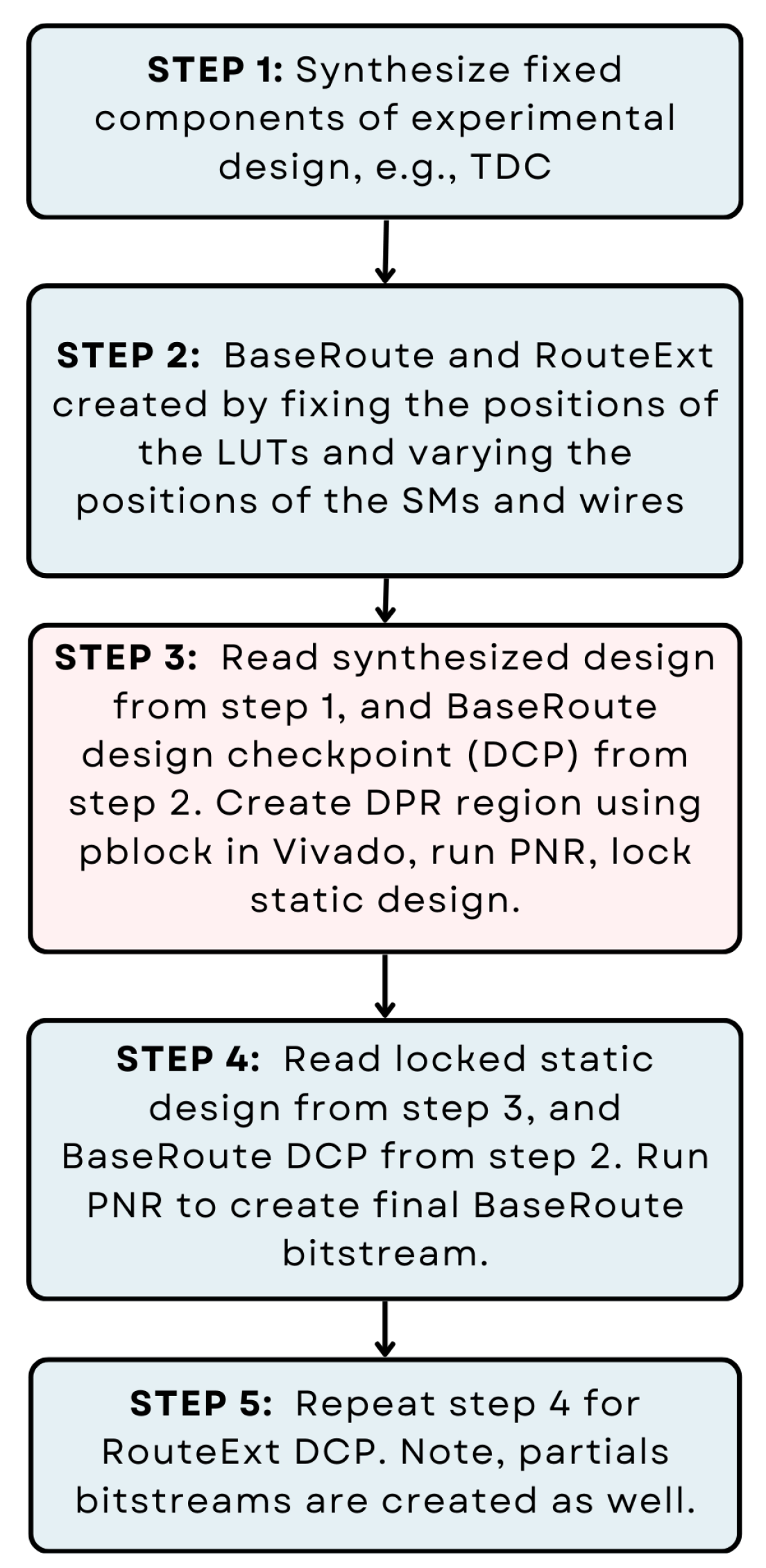
Figure 5.
Data post-processing algorithm applied to data from the Hand-Crafted experiments.
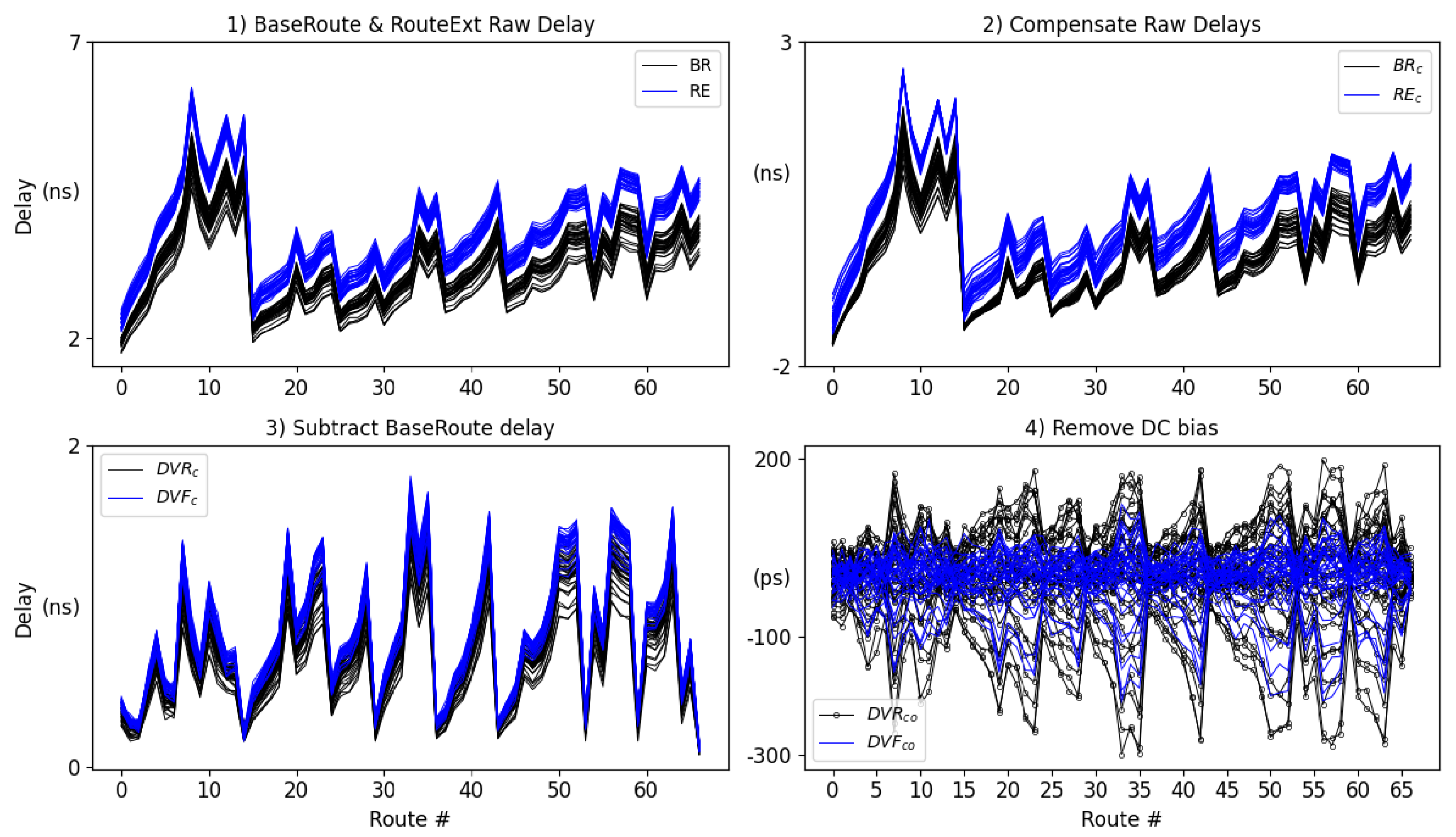
Figure 6.
Data post-processing algorithm applied to data from the Tool-Crafted experiments.
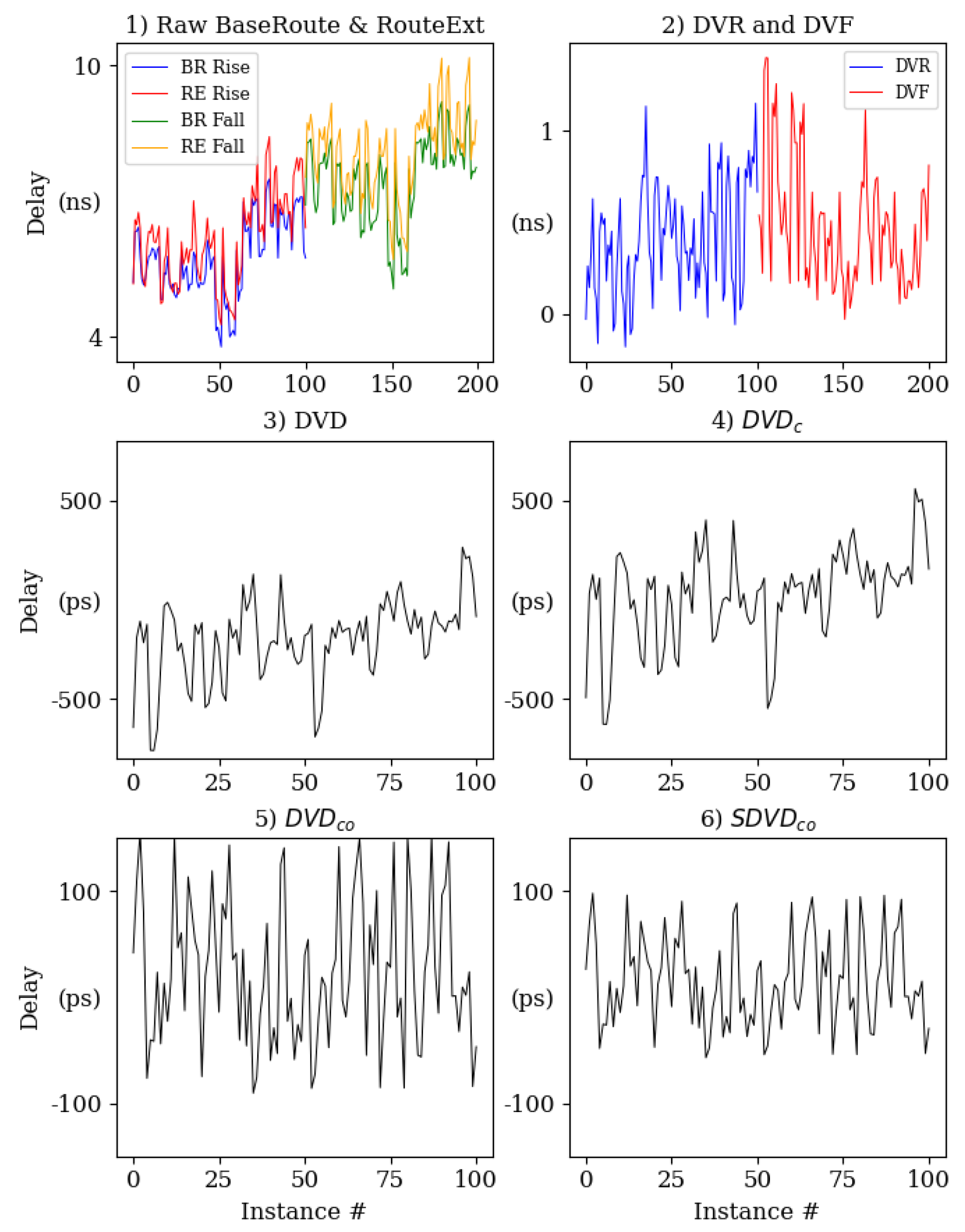
Figure 7.
Illustration of the bit-flip avoidance bitstring generation algorithm.
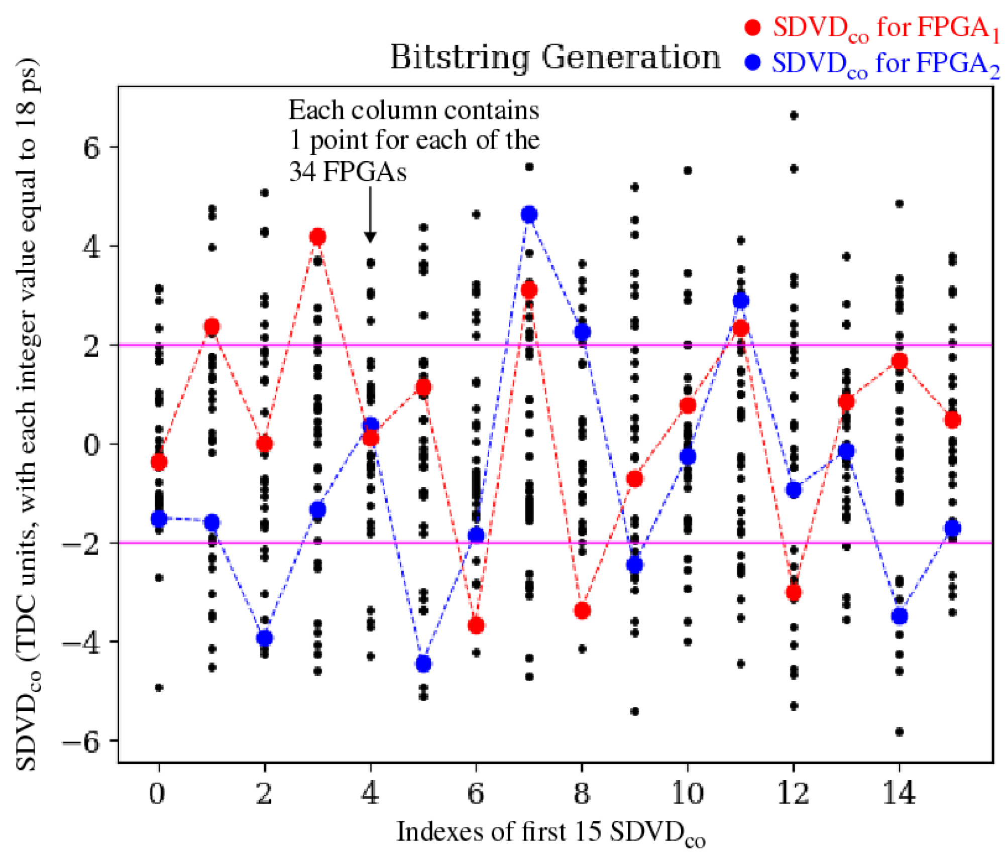
Figure 8.
Physical characteristics of the Hand-Crafted routes, showing the number of SMs in the lower portion of the bars and the number of unit-sized wires in the upper portion.
Figure 8.
Physical characteristics of the Hand-Crafted routes, showing the number of SMs in the lower portion of the bars and the number of unit-sized wires in the upper portion.

Figure 9.
Vivado implementation view of the BaseRoute SM (left) and RouteExt SM (right) for Hand-Crafted route 66, showing the only change in the entire route is a change to the ’bounce’ which occurs within the SM.
Figure 9.
Vivado implementation view of the BaseRoute SM (left) and RouteExt SM (right) for Hand-Crafted route 66, showing the only change in the entire route is a change to the ’bounce’ which occurs within the SM.
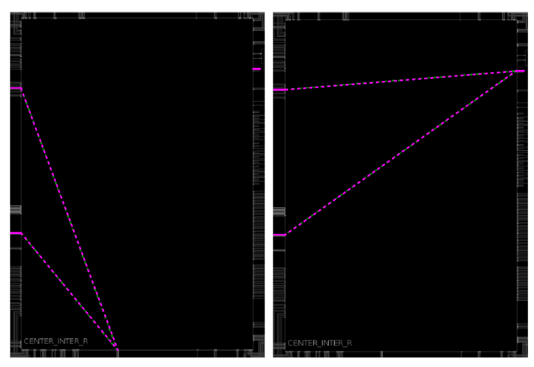
Figure 10.
Correlation analysis of physical path characteristics against the level of entropy measured in the path composed of SMs and wires. The Pearson’s correlation coefficient is 96% for the rise and 89% for the fall.
Figure 10.
Correlation analysis of physical path characteristics against the level of entropy measured in the path composed of SMs and wires. The Pearson’s correlation coefficient is 96% for the rise and 89% for the fall.
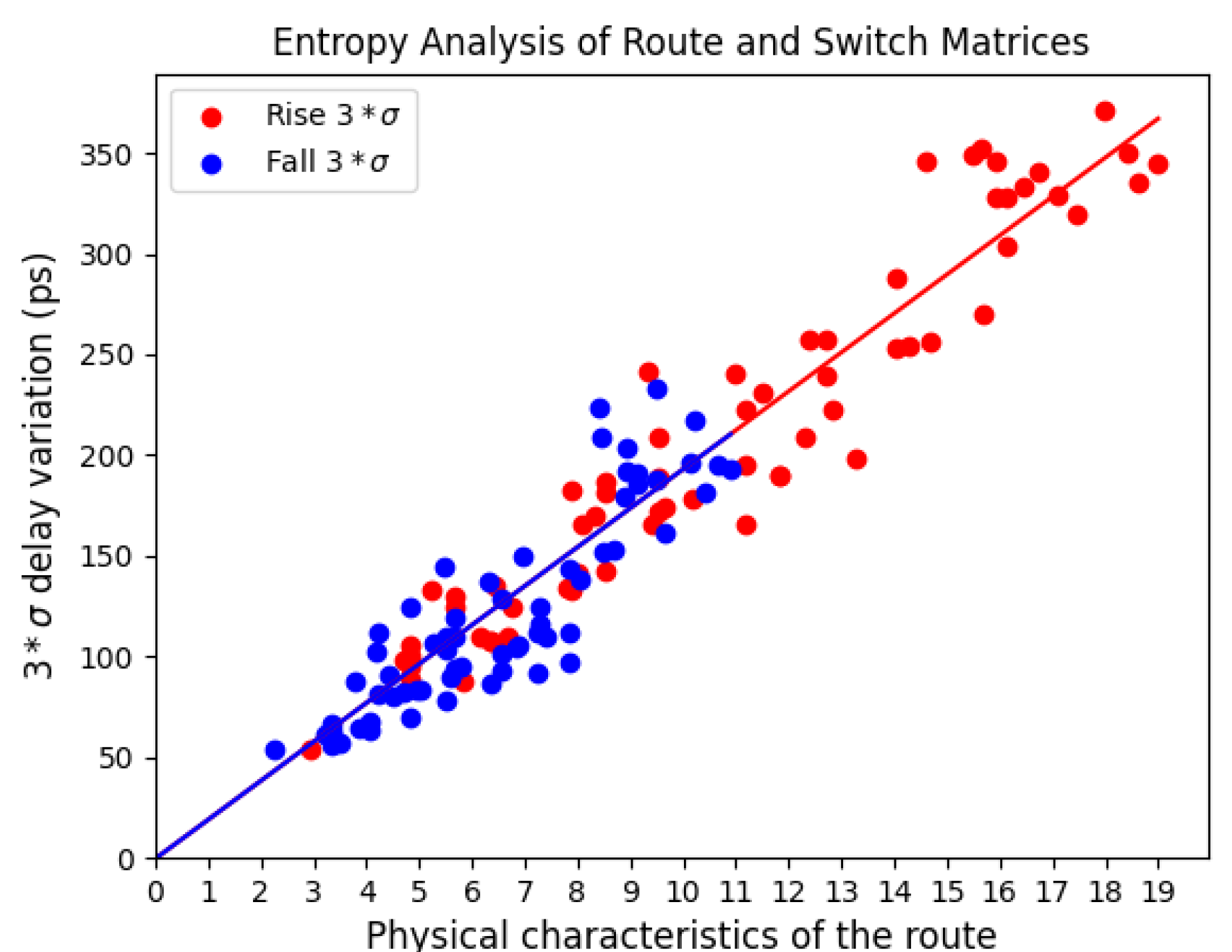
Figure 11.
Distribution of inter-chip hamming distances computed using all possible pairing of bitstrings from the 34 FPGAs.
Figure 11.
Distribution of inter-chip hamming distances computed using all possible pairing of bitstrings from the 34 FPGAs.
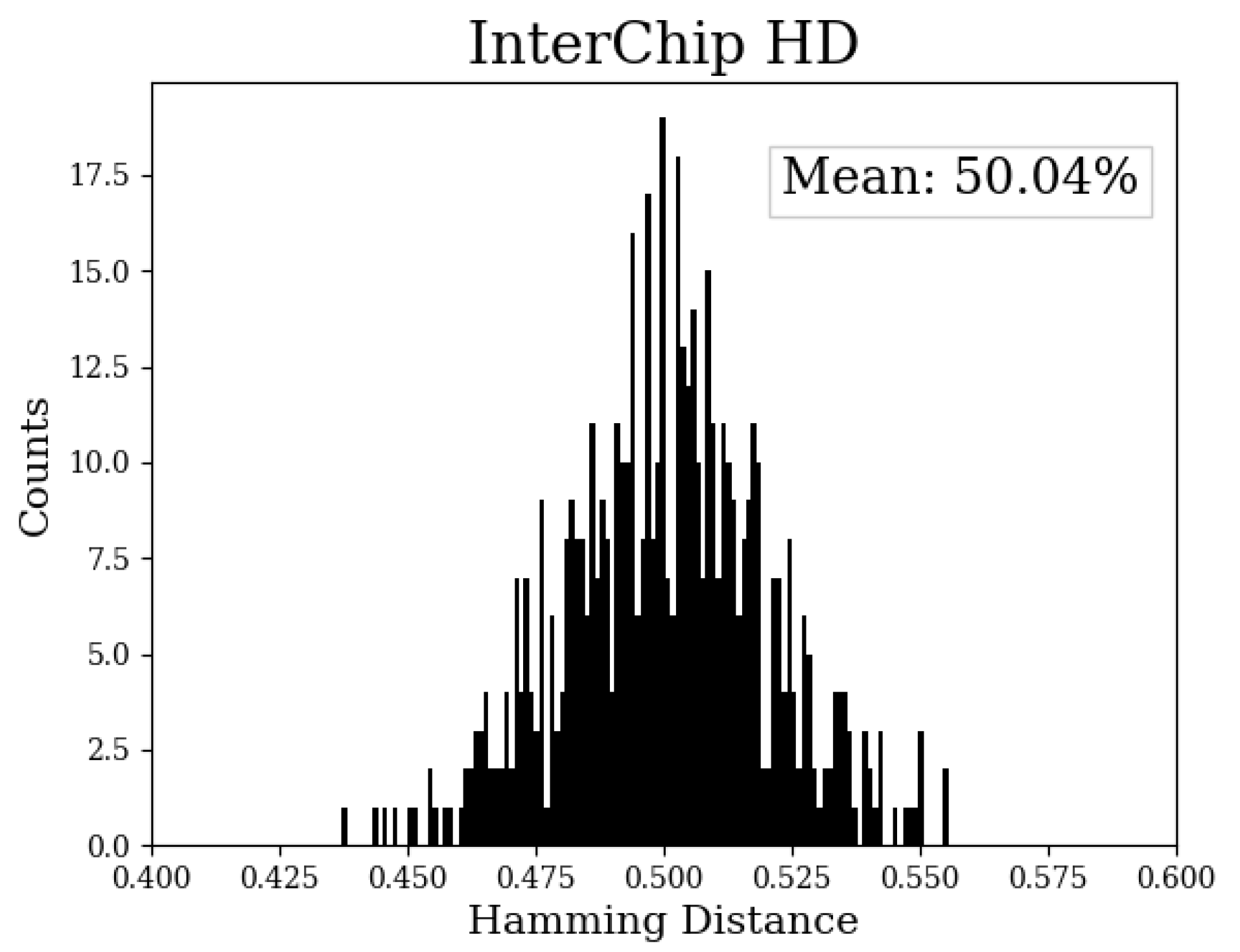
Figure 12.
NIST statistical results for bitstrings of length 128 from the Tool-Crafted Experiment.

Disclaimer/Publisher’s Note: The statements, opinions and data contained in all publications are solely those of the individual author(s) and contributor(s) and not of MDPI and/or the editor(s). MDPI and/or the editor(s) disclaim responsibility for any injury to people or property resulting from any ideas, methods, instructions or products referred to in the content. |
© 2024 by the authors. Licensee MDPI, Basel, Switzerland. This article is an open access article distributed under the terms and conditions of the Creative Commons Attribution (CC BY) license (http://creativecommons.org/licenses/by/4.0/).
Copyright: This open access article is published under a Creative Commons CC BY 4.0 license, which permit the free download, distribution, and reuse, provided that the author and preprint are cited in any reuse.


