Submitted:
02 January 2024
Posted:
03 January 2024
You are already at the latest version
Abstract
Passive balancing is a traditional choice for lithium-ion battery packs although it is regarded as highly inefficient. One opportunity to improve traditional balancing in sub-medium size battery packs is to combine two balancing methods: passive and active. Statistical analysis have been performed to rationalize battery pack division in smaller packs and use of higher level selective charging method to decrease losses of passive balancing. An experimental balancing prototype have been designed and tested for efficiency. Results indicate energy performance degradation if cells of the pack are with low capacity variation. Proposed balancing approach could improve performance under high cell mismatch conditions.
Keywords:
lithium-ion
; batteries
; passive balancing
; active balancing
; cell balancing
1. Introduction
All lithium-ion based batteries require some sort of management system for safety and basic functionality. In the case of multi-cell batteries, the management system must perform cell balancing as well. A wide variety of different cell balancing methods can be found in scientific literature. Multiple authors have proposed classification of given methods based on operation principles, charge exchange directions, used components [1,2,3,4,5]. A variety of technologies rely on safe operation of batteries [6,7,8,9], for example, [10] proposes a modular concept of battery charger for personal mobility vehicles for its safe operation and, in the same time, providing its expandability, but [9] reveals peculiarities if this charger. Despite the vast amount of developed methods both simulations and experimental validation shows that there is no clear winner method which would prevail in all fields: cost, simplicity, size, reliability, efficiency or efficacy, easy implementation and modularity.
It seems that the research of new methods is still ongoing and the main reason for new research often is cited to be the need for higher efficiency. Passive balancing is a traditional practical application choice although it is inherently inefficient – it converts any misbalance into losses. Technically its efficiency is zero as all of exchanged energy is lost as heat if compared to other switch mode converter based methods [11]. A more appropriate efficiency calculation is the relative (or absolute) amount of lost energy. Often research articles use exceedingly high misbalance conditions to emphasize losses of passive balancing [12,13,14]. However manufacturers’ datasheets show that cell parameters nominally have dispersion less than 2% which is approved by measurements [15,16]. If cells are sorted prior to pack assembly, even lower mismatch can be achieved which would result in lower need for balancing performance. Eventually even identical cells would still suffer from effects of thermal gradient across the battery pack as well as from differences in management system leakage currents and interconnection resistances. These factors depend on the size of the pack – generally, smaller packs are easier to maintain.
Here a small, 12-cell battery pack is discussed. The pack is intended to be used in a power-assist type wheelchair to power a modular in-wheel motor. The pack is composed of NCR18650GA (3.3 Ah) lithium-ion cells, which would normally be connected in 12S configuration. If a battery with higher capacity is required then another cell is added to each existing, producing 12S2P configuration with double Ah rating at the same voltage. Typically, such battery packs are equipped with traditional passive balancing to deal with cell mismatch. As noted previously, scientific literature indicates that the given method is inefficient. It would be reasonable to explore techniques which could be used to lower the losses. One way to improve the performance would be to add an extra balancing method to split pack into sub-packs as losses of passive balancing are related to number of cells in series. Here a mixed two-layer balancing method is implemented and tested. The method is a hybrid approach which uses passive balancing for the lower layer while multi-secondary winding transformer method is used to perform selective charging at higher level. Selective charger part can be implemented in an external charger unit while the battery pack needs just a corresponding connector to connect all sub-packs to multiple charger outputs.
2. Materials and Methods
2.1. Cell Balancing
In scientific literature, battery cell balancing methods are split into passive and active balancing. Passive balancing is rather simple as it uses a resistor or a transistor in linear mode to dissipate excessive charge. A more suitable names to this balancing method are switched resistor, shunting resistor, bypass resistor or dissipative resistor method. All other balancing methods are regarded as active methods which can be further split into selective charging/discharging methods, capacitive charge transfer methods, inductive charge transfer methods, and transformer-based charge transfer methods.
2.1.1. Switched Resistor Balancing
Switched resistor balancing (Figure 1) utilizes a dissipation element (resistor) and a switching element per cell – both elements can be combined and implemented as a single transistor. If the voltage or charge level of a given cell is too high, then the switch is activated to dissipate the excessive stored energy – it is lost as heat. Usually, the cell voltage level is used as the balancing criterion as the estimation of state of charge of individual cells is more difficult and it can be troublesome to charge all cells to the same SoC if just switched resistor balancing is used. Switched resistor balancing is typically used during the end-phase of charging process when cells reach the terminal voltage. Due to various reasons (capacity and impedance mismatch during manufacturing, temperature gradient during operation, different ageing, etc.) cells of the battery are not identically charged and have different voltages. When the first cell reaches max voltage, the charging should be stopped to prevent overcharge which can result in catastrophic consequences. When the charging is stopped, a switched resistor is used to slightly discharge a given cell and bring its voltage closer to other cells. After the voltage of given cell has decreased to the level of other cells or to a defined safe level, the charging is initiated once again. Alternatively, charging current can be decreased to match the balancing current thus fully charged cells remain charged while other cells are still being charged. This process is repeated until voltages of all cells are the same within set boundaries. As this approach converts excessive charged energy to heat, it is generally considered to be wasteful and inefficient. Despite this consideration, the switched resistor balancing is widely spread and used in most battery packs.
2.1.2. Multi Secondary Winding Transformer Balancing
This method which is also called ramp converter [17] can operate as charge transfer and as selective charger balancer. If operated as charge transfer circuit, it can be used in various modes of operation: pack-to-cell, cell-to-pack, cell-to-cell. Here the interest lies in selective charging capability – by naturally distributing charging current, an equal voltage for all cells is achieved. The circuit consists of a transformer whose primary side can be supplied by the battery pack (pack-to-cell balancing) or by external power source – in this case the transformer is sized to be able to supply full charging current while often it is much smaller to accommodate balancing currents during charging or discharging. In the simplest form, each cell of the pack is connected to a separate secondary winding equipped with a rectifier (Figure 2).
One of the main advantages of this method is simple control as the charging/balancing current is naturally distributed according to voltage levels of individual cells – cells with lower voltage are charged with higher current and vice versa. However, for practical applications there are some serious disadvantages: there is a need for bulky and expensive transformer and as the cell number increases there should be more secondary windings – it quickly becomes impossible to fit required number of windings on a bobbin of as single transformer.
Multi-layer balancing scheme is not a new concept. Multi-layer or multi-stage capacitive charge transfer or shuttle method is already well known. However mixed multi-layer methods which use different approaches for each layer are yet to be explored.
One possibility is to combine switched resistor balancing for the lower level and multi-secondary winding transformer for higher level [18]. The higher-level balancing is configured as a selective charger which essentially splits pack into sub-packs or modules (Figure 6). Each module is equipped with switched resistor balancing performing final equalization. The switched resistor losses should decrease due to smaller cell stack however to understand loss origin an analysis of switched resistor loss cause has to be made.
2.2. Losses of Switched Resistor Balancing
When charging a battery, balancing power loss Ploss of switched resistor method is zero while no balancing resistor is activated – this amounts for most of time of the charging procedure if cells are equal and closely balanced. During charging, once the first cell reaches full voltage/balancing voltage (Vbal), its balancing resistor is activated and charging current Ichg is decreased to match the balancing current Ibal (an idealized case) (1).
As a result, the state-of-charge (SoC) of given cell does not change while balancing losses appear according to (2).
Gradually, more cells reach balancing voltage, and add to the total power loss which can be calculated using (3). Eventually n−1 cells are full and just one cell is being charged – Ploss is at max value and can be calculated using (4). The charging current is reduced to zero (charging is stopped) once the last cell reaches full voltage hence Ploss becomes zero as well.
The balancing power loss is a discrete function as can be seen in 20-cell battery example in Figure 3. The power loss gradually increases in steps from zero to its max value when 19 cells (n−1) are full/being balanced. The duration of each step is related to cells’ SoC mismatch during charging operation.
The total energy loss during balancing operation is more useful variable as it can be easily compared to total energy loss of other balancing methods. Generally, balancing energy loss Eloss is an integral of balancing power loss over balancing time full (5).
The integration interval is from the beginning of balancing operation to the end when last cell reaches its full voltage. As the Ploss(t) is a discreet function then Eloss can be expressed as a sum of individual Ploss levels (6).
Capacity difference ΔC is specific to every cell – it shows the relative difference in capacity in respect to the previous cell and the one which is being balanced. For the first cell ΔC1=0 and each next ΔCx value can be calculated as difference between previous Cx−1 and given cells’ Cx value. If ΔC value span and distribution is narrow, then resulting Eloss will be small. Equation (6) can be used to calculate energy losses of a 20-cell battery with normal cell capacity distribution at different known capacity variations. Figure 4 shows the obtained graph.
10 sets of random normal distribution capacities were generated for each of capacity variation points from 0.5 % to 4 %. The line shows average energy losses while dots mark the max and min losses of performed calculations. Graph shows that if capacities of battery cells have normal distribution, then balancing losses will increase linearly with increase in cell capacity variation. To understand and analyze the potential losses of different types of battery packs, in-depth statistical analyses were executed. In this given case, different dispersion ranges were taken into account to understand the variation of the potential losses. One common measure of dispersion is the standard deviation, which is the square root of the variance of the cell capacity in the pack. In this case, the data follows a normal distribution, then the standard deviation can be used to create a formula that describes the dispersion. After this analysis, the approximation (7) was calculated to obtain the average losses P% (in %) depending on the capacity dispersion CS (percentage of cell capacity variation).
The overall graph where the energy losses are shown accordingly to different capacity variations is shown in Figure 4. With the blue line, the maximum graph is represented and with the gray line, the minimum values are shown based on the calculations. The middle line is the average value represented by (7).
To show the whole range of the 20-cell pack potential energy losses for the stabilization of the pack a equation (8) was created.
To have a better understanding of the different battery packs and options a more in-depth calculator and statistical analysis were made taking the same methodology as the previously described one for the 20-cell battery pack and repeated for different battery packs. Taking the range starting from packs containing only 2 cells and going up to whole 20 cell pack. After all the calculations then the 3D model was constructed with all the data. As can be seen in Figure 5 then in this graph is shown the energy losses for the balancing of the whole battery pack. These balancing losses in the graph dependent on both - cell unit count in the battery pack and the cell capacity variation within the pack.
As seen in both graphs then the growth of the energy losses for balancing of the whole battery pack is upwards sloping with a positive dependency on the element count and the percentage of the capacity variation.
2.3. Hardware of Mixed Two-Level Balancing
The addition of multi-secondary transformer topology introduces new losses although contrary to switched resistor losses, these losses are not inherent but depend on actual elements, topology and switching control. To obtain real-life practical results it was decided to perform an experimental investigation using 12-cell battery pack which was equipped with a mixed balancing system as shown in Figure 6. The battery pack was designed to be able to split in different sub-packs producing 1×12S, 2×6S, 3×4S, 4×3S, 6×2S configurations, where first digit indicates the number of sub-packs per battery while the second number indicated number of series cells per sub-pack. The 1×12S configuration is the same as traditional 12S configuration.
The charger-balancer hardware can be split into three parts: primary side; secondary side; BMS side - as shown in Figure 6. The practical implementation of the power part of multi-secondary winding transformer balancing circuit is shown in Figure 7. The BMS hardware is straightforward: a commercial Texas Instruments bq76940 evaluation module was used. The central element of the evaluation module is Texas Instruments bq76940 battery monitor IC which performs analog front-end (AFE) functions: cell voltage measurement; pack current measurement; temperature measurement; hardware overcurrent, short circuit, overvoltage, undervoltage and secondary fault protection; charge and discharge switch control; integrated cell balancing. The balancing feature is upgraded by external FETs and 100 Ω resistors which would dissipate 0.18 W at 4.2 V. The board contains shunt current measurement and power FETs for charge/discharge control. The AFE IC must be controlled by another controller to operate. The evaluation board has Texas instruments bq78350 battery management controller companion IC installed – this part can be preprogrammed to control the AFE IC. Alternatively, I2C interface can be used to connect an external controller to the evaluation module and to the AFE IC – this is option with Raspberry Pi Pico W controller was used for this experiment. The BMS was configured to provide two main functions: balance cells using switched resistor method; analyze voltage measurements of all cells to control the charger. Additionally, the measured voltages are logged for further analysis. The balancing function during charging was implemented as follows. Voltages of all cells are measured every 0.25 seconds. If the voltage of any cell is higher than setpoint (4.195 V), then BMS board power FETs are turned off and corresponding balancing resistor (or multiple resistors) is turned on. Once the voltage of corresponding cell is lower that setpoint (4.150 V), the power FETs are turned on and charging is continued. The process is continued until voltages of all cells are higher than full charge setpoint (4.190 V). When all cells are full, then power FETs are turned off until the system is reset. During discharge, the voltages are constantly measured and logged. Once any of the cells reach the empty setpoint (2.800 V) the power FETs are turned off until the system is reset. The primary side of the charger circuit is enabled and disabled by the BMS controller – if the power FETs are turned on, then charger is enabled and vice versa.
The primary side of the charger circuit was designed as a half-bridge with 32 V DC at it input, which is provided by external power supply. The primary side power elements were selected to be able to transfer at least 100 W or 3.2 A at 32 V input voltage. Two parallel NTD3055L104T4 MOSFETs with an isolated driver were used for each switch. ETD34 core with 3C90 ferrite material was used as the base of transformer. When equation (90) is used with Vin=32 V, f=50 kHz, Bmax=1500 G, Ac=0.916 cm2 the result is 5.8 turns.
It has to be taken into account that the output voltage of the transformer has to be higher than full charge voltage (12∙4.2=50.4 V) at least by two diode drops (1.4 V). If the pack is split into 12 sub-packs then there would be 12∙0.7=8.4 V additional voltage drop, which results in 58.8 V total transformer output voltage. When this voltage is used in transformer voltage/turns equation (10), then the resultant number of secondary turns-11 is not sufficient for all sub-pack configurations. If each cell of the pack is to be charged with a separate transformer output, then the number of windings must be dividable by the number of cells: 12. From this perspective equation (10) can be used again as in (11) to calculate primary turns if total amount of secondary turns is set to 12. This produces 6.5 turns which rounds up to 7 which in turn adds extra margin for output voltage which could be consumed by wiring, current shunts and power FETs drops.
Overall, the transformer is oversized mainly to be able to accommodate multiple secondary windings as required by the balancing topology. The windings are wound using 120∙0.1 mm litzwire for secondary and 150∙0.1 mm for primary. Each secondary winding is equipped with a Schottky diode full bridge rectifier and 8.8 µF filter film capacitor. 0.1 ohm shunt resistor with ZXCT1080E5TA high-side current monitor is used to transduce the charging current of each sub-pack. BMS board contains another shunt for whole pack current measurement. The multi-secondary winding converter is locally controlled using MSP430F5172 microcontroller. The microcontroller acquires charging current of each sub-packs and adjusts PWM duty cycle of primary side switches according to current and voltages acquired by bq76940 board.
3. Results
The performance evaluation of the developed system was done using experimental testing of two battery packs. One pack was made of 20S configured 40 Ah LFP prismatic cells. This pack was made to be able to be split into 4×5S configuration for selective charging. The other pack was made of twelve 18650 size NMC cells in 12S configuration with possibility to connect to each cell individually. The charging/discharging energy was selected to be the performance indicator. Precision power analyzer PPA5530 from Newtons 4th was used to measure the energy spent during charging. It can be assumed that there should not be significant battery degradation between few cycles hence the energy amount spent during charging can be an indicator to compare two charging methods: traditional switched resistor balancing and mixed two-layer balancing.
Testing with the 20S LFP pack was done in several steps. First the pack was subjected to full discharge using an electronic load and power analyzer to obtain discharged energy amount. Then the pack was charged using a laboratory DC power supply to feed half bridge charger. The pack was equipped with switched shunting resistor balancing and charging power/energy was measured before the half bridge converter. The charging was stopped once all cells of the pack had reached the balancing voltage. Afterwards the pack was once again discharged and energy was measured. This test revealed that it is possible to retrieve 81.4 % of the initial charging energy. The same test was repeated with a half bridge converter which has multiple secondary windings that are connected to split battery pack. After the test it was calculated that the retrieved energy was 78.6 %.
12S NMC pack was tested using bq76940 board and RPi Pico for the balancing purpose. The balancing was initiated once the first cell reached balancing voltage. Charging was stopped while there was active balancing. The balancing and charging was stopped once all of the cells have reached balancing voltage at least once – typically at the end not all cells were being discharged using the switched resistor. A laboratory power supply in constant current/constant voltage mode was used to supply charging power and an electronic load in constant current mode was used to discharge the pack. The same power analyzer was used to measure charging and discharging energy which was 132.60 Wh and 118.65 Wh respectively. This produces 89 % energy cycle efficiency. bq76940 board was used to obtain charging voltage graphs of all cells. The result is shown in Figure 8.
4. Discussion
The initial statistical calculations reveal that the losses of switched balancing increase linearly both in respect to series cell connection and cell capacity variation. Hence it should be possible to decrease switched resistor balancing losses if a pack is split into smaller sub-packs. Theoretically, as all of the cells of the pack is connected to separate charging output, the switched resistor balancing losses become zero as there actually is no need for given balancing method – all balancing is achieved by multi-secondary winding transformer balancing. However, this is not beneficial in all cases if any at all. Each secondary winding is equipped with a rectifier which has to conduct the full charging current which in turn produces full conduction losses. If there is just one charging output/one secondary winding, then there is one relative unit of rectifier conduction losses. If all 12 secondary windings are used, then rectifier conduction losses are 12 relative units as all cells have the same charging current during the constant current bulk charging phase.
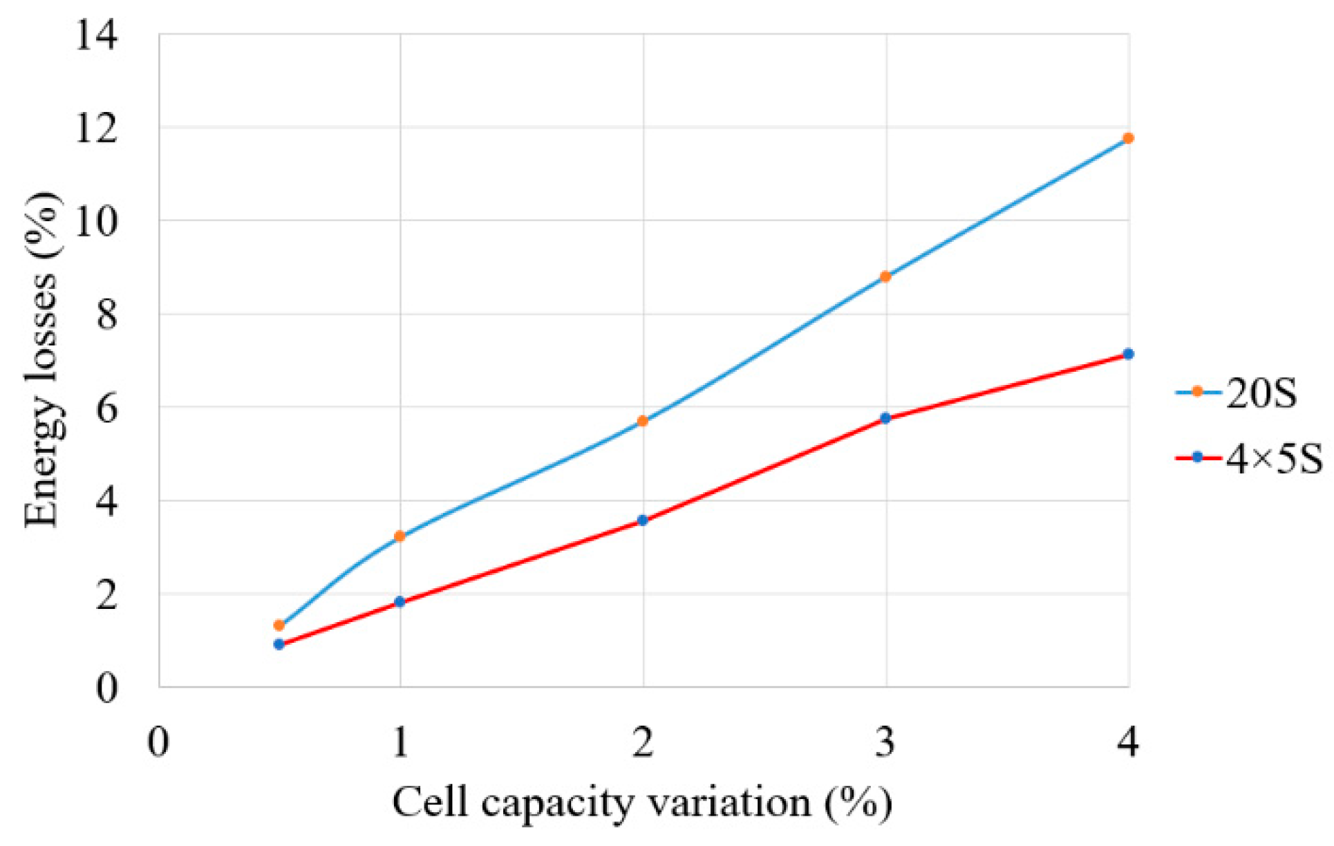
For given mixed two-layer balancing to be more efficient than traditional switched resistor balancing, certain conditions must be met. The initial pack analysis of Figure 4 was continued by divining whole pack into four sub-packs and repeating the calculations. As shown in Figure 9 split pack version has smaller switched resistor balancing losses and these losses depend linearly on the capacity variation. A conclusion can be drawn that it is beneficial to split packs which have wide capacity variation while packs with closely balanced cells will have very little room to benefit for sub-pack construction.
Equation (12) shows the condition to meet mixed two-layer superiority. The losses of multi secondary winding transformer EMST has to be smaller than loss improvement which is achieved by decreasing the traditional switched resistor losses ESR_full to split pack switched resistor losses ESR_split.
Technically EMST value could be improved by using active synchronous rectification however it is not likely that the improvement will be sufficient to overcome the losses generated throughout whole bulk charging phase. If the pack is sufficiently balanced, then the need for selective charging is minimal.
It can be concluded that the introduction of additional transformer windings and rectifiers have lowered the charger efficiency more that efficiency was improved by dividing the pack into sub-packs. The introduction of additional method increased total losses and in given case did not improve overall efficiency.
Author Contributions
Conceptualization, K.V.; methodology, K.V. and E.G.; software, K.V.; validation, K.V. and I.G.; formal analysis, E.G.; investigation, K.V.; resources, K.V.; data curation, K.V.; writing—original draft preparation, K.V.; writing—review and editing, I.G.; visualization, K.V.; supervision, K.V.; project administration, I.G.; funding acquisition, I.G. All authors have read and agreed to the published version of the manuscript.
Funding
The preparing of this publication is supported by the European Regional Development Fund (ERDF) within the contract Nr. 1.1.1.1/16/A/147 “Research and Development of Electrical, Information and Material Technologies for Low Speed Rehabilitation Vehicles for Disabled People”.
Data Availability Statement
The data presented in this study are available on request from the corresponding author. The data are not publicly available due to lack of well organized material.
Conflicts of Interest
The authors declare no conflict of interest. The funders had no role in the design of the study; in the collection, analyses, or interpretation of data; in the writing of the manuscript; or in the decision to publish the results.
References
- J. Gallardo-Lozano, E. Romero-Cadaval, M. I. Milanes-Montero, and M. A. Guerrero-Martinez, “Battery equalization active methods,” J. Power Sources, vol. 246, pp. 934–949, 2014. [CrossRef]
- Z. G. Kong, C. B. Zhu, R. G. Lu, and S. K. Cheng, “Comparison and evaluation of charge equalization technique for series connected batteries,” in PESC Record - IEEE Annual Power Electronics Specialists Conference, 2006. [CrossRef]
- M. Daowd, N. Omar, P. van den Bossche, and J. van Mierlo, “A review of passive and active battery balancing based on MATLAB/Simulink,” Int. Rev. Electr. Eng., vol. 6, no. 7, pp. 2974–2989, 2011.
- J. Cao, N. Schofield, and A. Emadi, “Battery balancing methods: A comprehensive review,” in 2008 IEEE Vehicle Power and Propulsion Conference, VPPC 2008, 2008, pp. 3–8. [CrossRef]
- M. Daowd, N. Omar, P. Van Den Bossche, and J. Van Mierlo, “Passive and active battery balancing comparison based on MATLAB simulation,” in 2011 IEEE Vehicle Power and Propulsion Conference, 2011, vol. 6, no. 7, pp. 1–7. [CrossRef]
- A. Avotins, O. Tetervenoks, L. R. Adrian, and A. Severdaks, “Considerations on Experimental Validation of Motion Detection Sensors for Street Lighting Systems,” in 2021 IEEE 62nd International Scientific Conference on Power and Electrical Engineering of Riga Technical University (RTUCON), 2021, pp. 1–6. [CrossRef]
- P. Maksimkins, A. Stupans, S. Krivisa, A. Senfelds, and L. Ribickis, “Implementation of a Classic Washout Filter for Robotic Large Range Motion Simulator using Cylindrical Coordinate System,” in 2021 IEEE 9th Workshop on Advances in Information, Electronic and Electrical Engineering (AIEEE), 2021, pp. 1–6. [CrossRef]
- M. Gorobetz, A. Potapov, A. Korneyev, and I. Alps, “Device and Algorithm for Vehicle Detection and Traffic Intensity Analysis,” Electr. Control Commun. Eng., vol. 17, no. 1, pp. 83–92, Jun. 2021. [CrossRef]
- A. Blinov, I. Verbytskyi, D. Zinchenko, D. Vinnikov, and I. Galkin, “Modular Battery Charger for Light Electric Vehicles,” Energies, vol. 13, no. 4, p. 774, Feb. 2020. [CrossRef]
- I. Galkin, A. Blinov, I. Verbytskyi, and D. Zinchenko, “Modular Self-Balancing Battery Charger Concept for Cost-Effective Power-Assist Wheelchairs,” Energies, vol. 12, no. 8, p. 1526, Apr. 2019. [CrossRef]
- F. Baronti, G. Fantechi, R. Roncella, and R. Saletti, “High-efficiency digitally controlled charge equalizer for series-connected cells based on switching converter and super-capacitor,” IEEE Trans. Ind. Informatics, vol. 9, no. 2, pp. 1139–1147, 2013. [CrossRef]
- T. H. Phung, A. Collet, and J. C. Crebier, “An optimized topology for next-to-next balancing of series-connected lithium-ion cells,” IEEE Trans. Power Electron., vol. 29, no. 9, pp. 4603–4613, 2014. [CrossRef]
- M. Y. Kim, C. H. Kim, J. H. Kim, D. Y. Kim, and G. W. Moon, “Switched capacitor with chain structure for cell-balancing of lithium-ion batteries,” in IECON Proceedings (Industrial Electronics Conference), 2012, pp. 2994–2999. [CrossRef]
- T. H. Phung, J.-C. Crebier, A. Chureau, A. Collet, and V. Nguyen, “Optimized structure for next-to-next balancing of series-connected lithium-ion cells,” in 2011 Twenty-Sixth Annual IEEE Applied Power Electronics Conference and Exposition (APEC), 2011, vol. 29, no. 9, pp. 1374–1381. [CrossRef]
- K. Vitols and E. Grinfogels, “Battery Batch Impedance Analysis for Pack Design,” in 2019 IEEE 7th IEEE Workshop on Advances in Information, Electronic and Electrical Engineering (AIEEE), 2019, pp. 1–5. [CrossRef]
- K. Vitols, E. Grinfogels, and D. Nikonorovs, “Cell Capacity Dispersion Analysis Based Battery Pack Design,” in 2018 6th IEEE Workshop on Advances in Information, Electronic and Electrical Engineering (AIEEE), 2018, no. 1, pp. 1–5. [CrossRef]
- Z. Ye and T. A. Stuart, “Sensitivity of a ramp equalizer for series batteries,” IEEE Trans. Aerosp. Electron. Syst., vol. 34, no. 4, pp. 1227–1236, 1998. [CrossRef]
- K. Vitols, “Efficiency of LiFePO4 battery and charger with a mixed two level balancing,” in 2016 57th International Scientific Conference on Power and Electrical Engineering of Riga Technical University (RTUCON), 2016, pp. 1–4. [CrossRef]
Figure 1.
Switched resistor balancing topology.
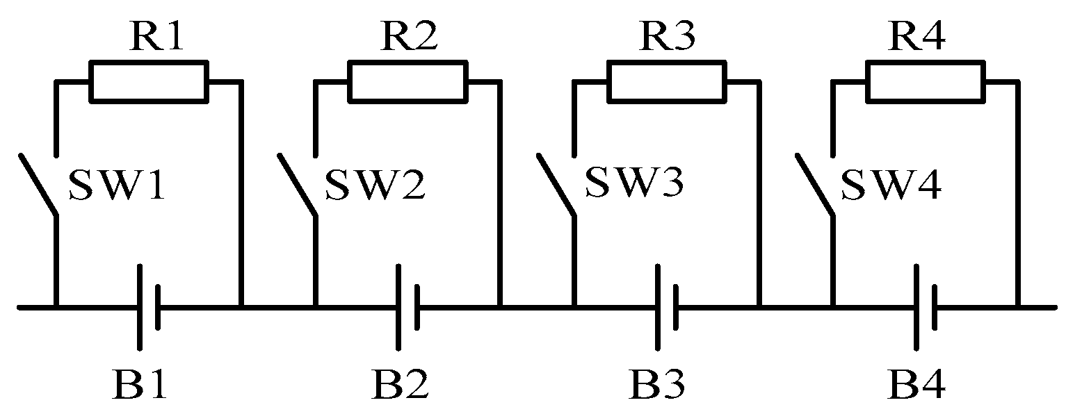
Figure 2.
Multi secondary winding transformer balancing topology.
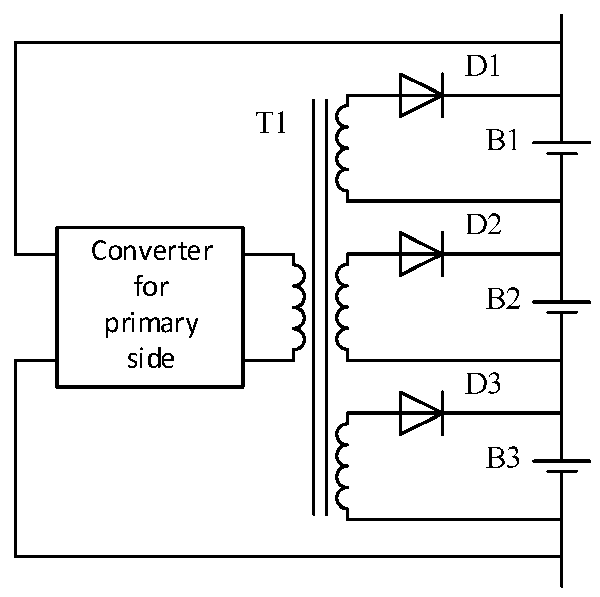
Figure 3.
Illustrative representation of power loss dynamics during switched resistor balancing.
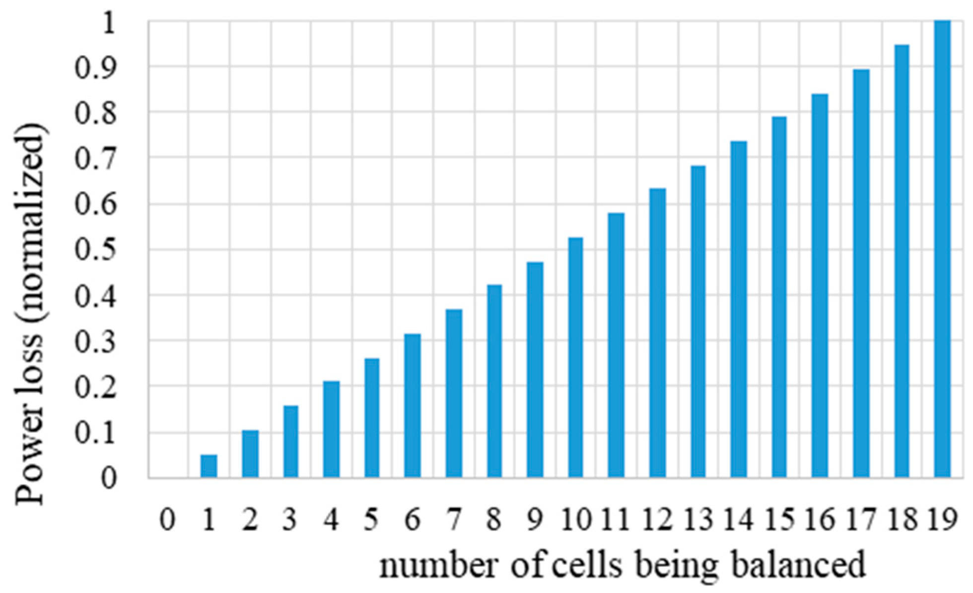
Figure 4.
Energy loss of a switched resistor balanced 20-cell pack with different cell capacity variations.
Figure 4.
Energy loss of a switched resistor balanced 20-cell pack with different cell capacity variations.
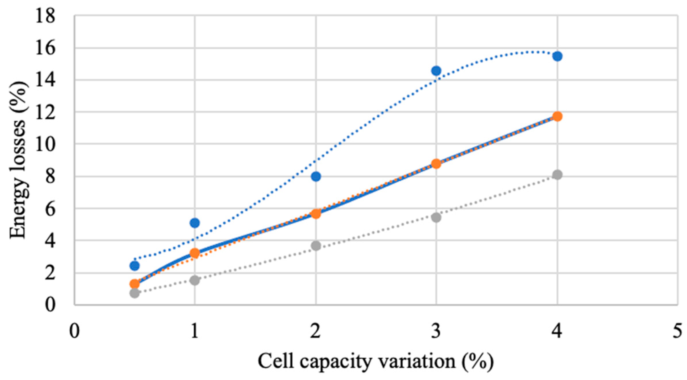
Figure 5.
Switched resistor balancing energy losses at different cell count and capacity variation.
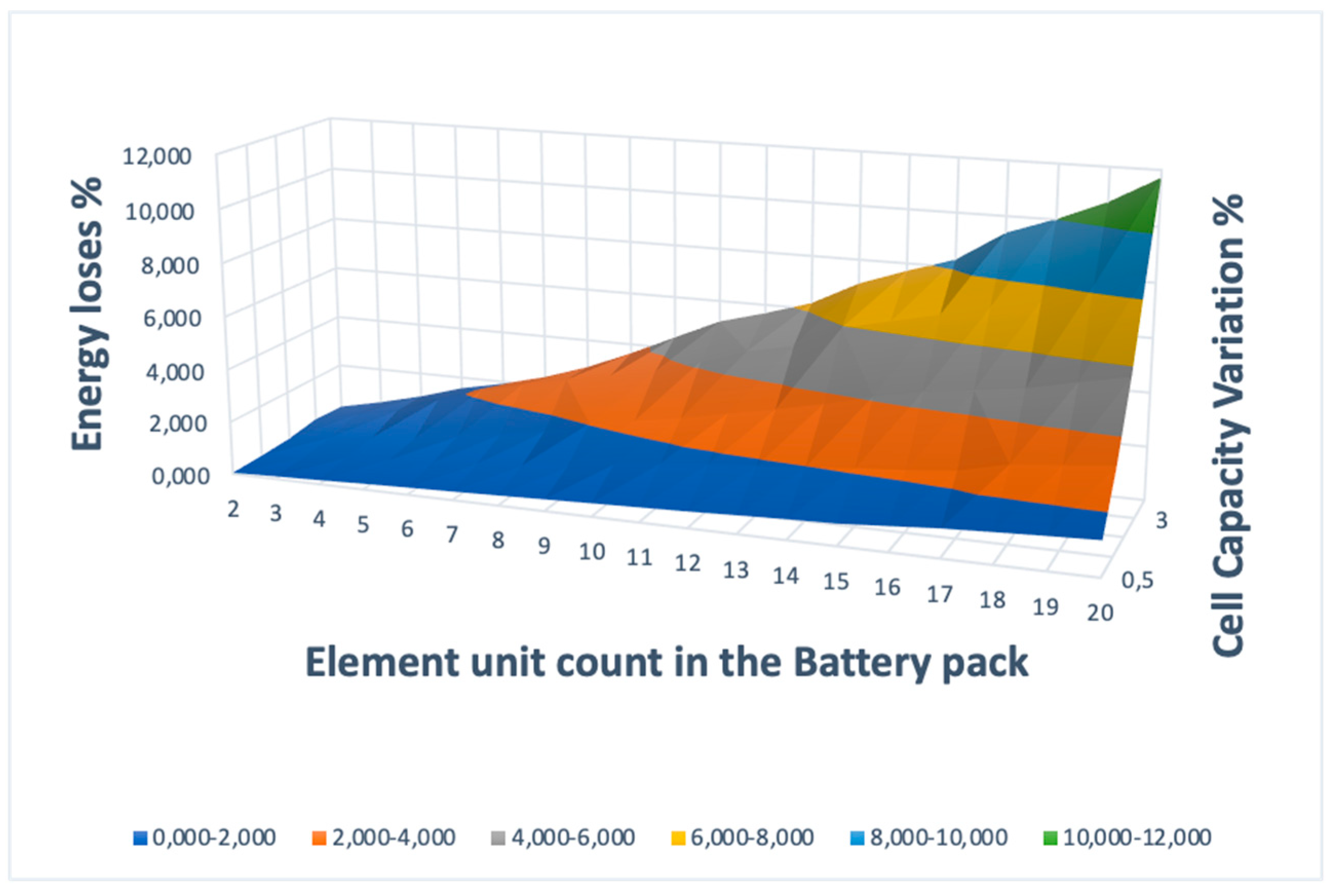
Figure 6.
Multi secondary winding transformer balancing topology.
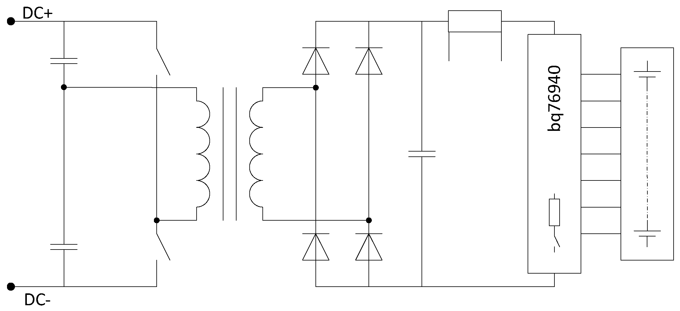
Figure 7.
Multi-secondary winding transformer power circuit with single secondary side.
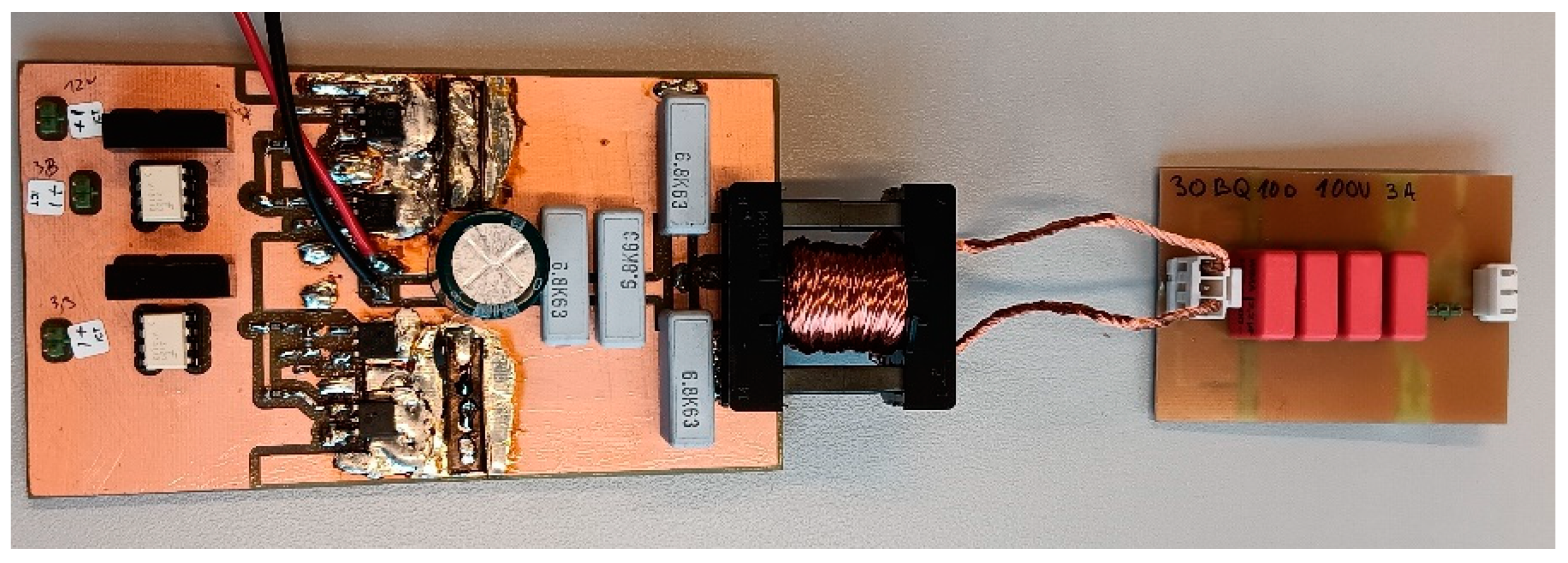
Figure 8.
Charging curve of 12S NMC battery pack.
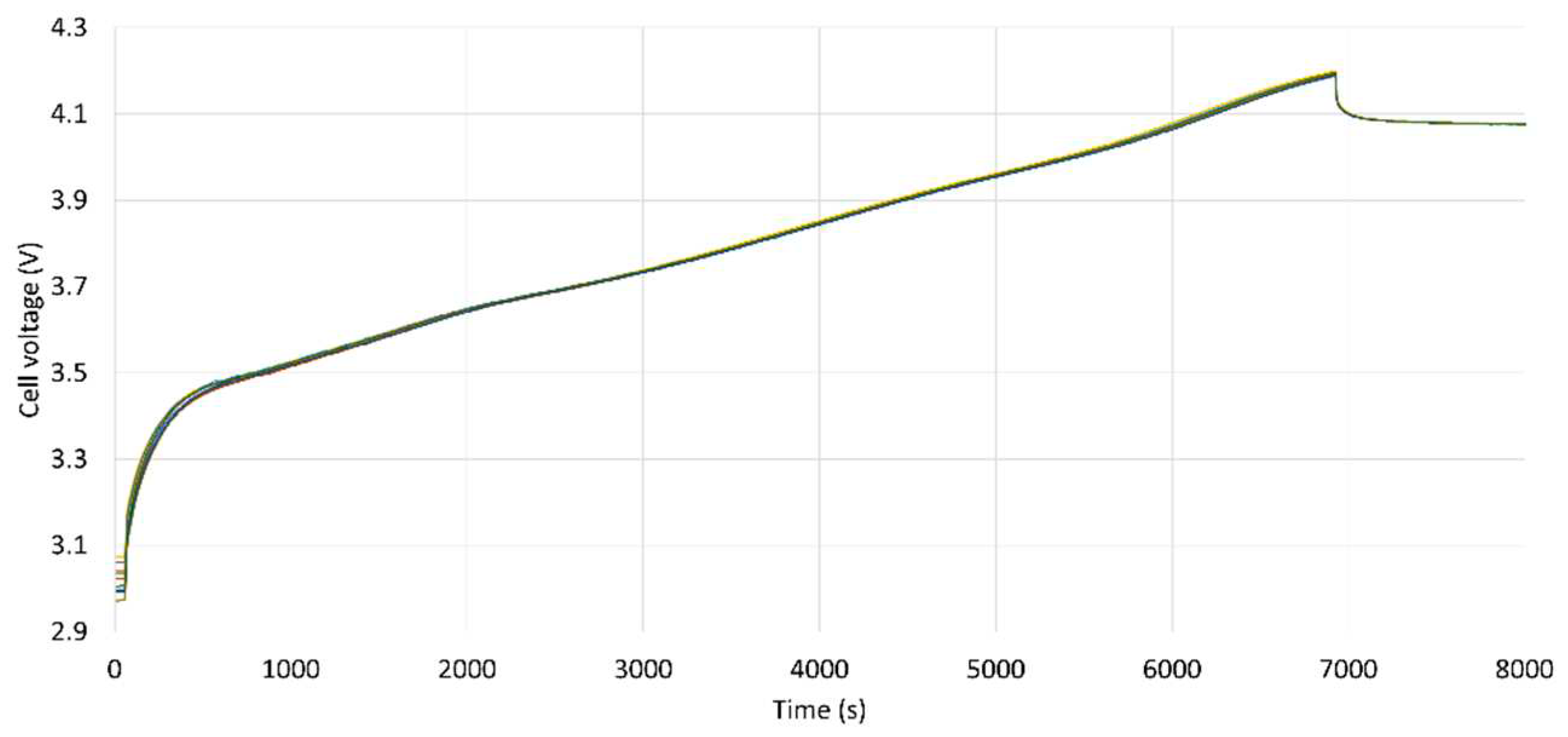
Figure 9.
Balancing energy losses with traditional and split switched resistor balancing.
Disclaimer/Publisher’s Note: The statements, opinions and data contained in all publications are solely those of the individual author(s) and contributor(s) and not of MDPI and/or the editor(s). MDPI and/or the editor(s) disclaim responsibility for any injury to people or property resulting from any ideas, methods, instructions or products referred to in the content. |
© 2024 by the authors. Licensee MDPI, Basel, Switzerland. This article is an open access article distributed under the terms and conditions of the Creative Commons Attribution (CC BY) license (http://creativecommons.org/licenses/by/4.0/).
Copyright: This open access article is published under a Creative Commons CC BY 4.0 license, which permit the free download, distribution, and reuse, provided that the author and preprint are cited in any reuse.


