

Submitted:
11 December 2023
Posted:
12 December 2023
You are already at the latest version
Abstract
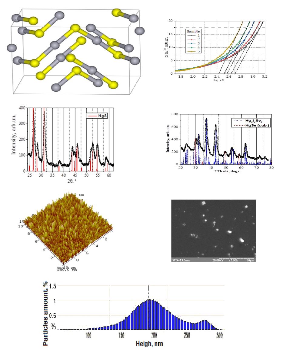
The main aspects of mercury sulfide and mercury selenide thin film synthesis using the chemical deposition method are considered. An analysis of various factors affecting film properties was conducted, including the study of how the nature of the substrate and its pre-treatment influence film properties. The effects of the working solution's temperature, deposition time, and annealing conditions on film characteristics were investigated. The impact of these parameters on the phase composition, as well as optical, electrical, and morphological properties of the films, is discussed and summarized. The paragraph also explains how the choice and concentration of initial reagents affect the parameters, characteristics, and properties of the obtained films.
Keywords:
mercury sulfide
; mercury selenide
; thin films
; chemical deposition
1. Introduction
The efforts of scientists involved in developing or enhancing functional materials can be more effective when directed not only towards synthesizing new chemical compounds but also towards creating materials with specific functional properties using known compounds and established technological methods. This is particularly applicable to semiconductor thin-film materials. The mass production of thin-film devices becomes feasible only when fabrication methods are technologically simple, cost-effective, easily controllable, and ensure high reproducibility of the material properties obtained.
The synthesis and investigation of semiconductor materials based on thin films of AIIBVI compounds (Zn, Cd, and Hg chalcogenides) have garnered significant attention. This is attributed to their unique properties, which strongly depend on various physical parameters, such as the size and shape of crystalline grains, composition, thickness, crystallinity, and microstructure.
Mercury chalcogenides are technologically intriguing materials with applications in infrared detectors, ultrasonic and gas sensors, catalysts, electrostatic reflecting materials, and solar cells. Despite their potential, they remain among the least researched. The scarcity of information on the synthesis and properties of mercury chalcogenide thin films can be attributed to the challenges encountered during their production. This difficulty arises from the inability to use typical complexing agents successfully employed for synthesizing cadmium and zinc chalcogenide films with specified properties. These agents are absent in macro- and microscopic bodies of the same chemical nature. Such limitations play a crucial role in hindering the advancement of nanotechnologies in contemporary science and technology.
A critical analysis of scientific articles on ScienceDirect reveals a notable increase in the overall number of publications dedicated to thin films. There is a growing interest in Group АІІВІV semiconductor materials, with subsequent applications in optoelectronics, photovoltaics, and solar elements. However, new publications regarding the research of mercury chalcogenide thin films are relatively rare.
Mercury sulfide and mercury selenide films exhibit high mobility and concentration of charge carriers, as well as thermomagnetic effects, photoelectron emission, and various photoelectric and optical absorption effects. These properties are crucial in thin-film photovoltaic converters, influencing photovoltaic sensitivity, the bandgap width (Eg) value, specific resistance (ρ), absorption coefficient (α), and volt-ampere characteristics.
Mercury sulfide exists in four polymorphic modifications: α-HgS with a trigonal structure (a = 0.4149 nm and c = 0.9495 nm), β-HgS with a cubic structure (a = 0.5851 nm), γ-HgS with a hexagonal structure (a = 0.701 nm and c = 1.413 nm), and δ-HgS, which exists at a pressure of 13 GPa and has a cubic structure (a = 0.5070 nm).
Mercury selenide (HgSe) also exists in four polymorphic modifications: α-HgSe, which has a cubic structure (a = 0.6087 nm), and the other three exist at high pressures ranging from 0.75 GPa to 28 GPa [1,2,3,4,5,6,7,8,9,10].
The lattice parameter (a) values for the cubic structures of HgS and HgSe closely align with those of ZnS (a = 0.5400 nm), CdS (a = 0.582 nm), PbS (0.593 nm), ZnSe (a = 0.5668 nm), CdSe (a = 0.604 nm), and PbSe (a = 0.6128 nm). This suggests the potential for obtaining solid solution films based on these compounds [11,12,13,14,15,16,17,18,19,20,21,22,23,24,25]. Additionally, there is the prospect of epitaxial growth of HgS and HgSe films on previously deposited films of these compounds, leading to relevant heterojunctions [31,34].
For HgS and HgSe films, the absorption coefficient (α) values range from 104 to 105 cm-1, while the specific resistance (ρ) varies between 104 to 105 Ω-cm and 103 to 104 Ω-cm.
2. Methods for Synthesizing HgS and HgSe Films
It is noteworthy that the bandgap width (Eg) values for HgS and HgSe films depend on the film’s structure and thickness. Therefore, the selection of a synthesis method becomes crucial to enable the production of films with reproducible properties. Currently, films of mercury chalcogenides, heterostructures, and solid solutions based on them have been successfully produced using a variety of methods, including vacuum deposition [26], magnetron sputtering [27], csathodic deposition [28], radiofrequency deposition [29], molecular beam epitaxy, and liquid phase epitaxy [30], electrochemical deposition [31,32,33], metalorganic compound deposition from the gas phase [27,30,34,35,36], spray pyrolysis [37], and chemical solution deposition [38,39,40,41,42,43,44,45,46,47,48,49,50,51,52,53,54,55,56,57].
As the utilization of physical methods entails the need for expensive equipment and the establishment of specialized conditions, the chemical deposition (CD) method from an aqueous solution was chosen for synthesizing HgS and HgSe films. This method was selected due to its simplicity, the ready availability and cost-effectiveness of chemical reagents, and its versatility – allowing any insoluble surface with free access to the working solution to serve as a substrate for deposition. Additionally, the use of low temperatures helps prevent undesirable processes such as oxidation, corrosion, thermal decomposition, and others.
The CD method, also known as controlled solution deposition or simply chemical deposition, relies on a chemical reaction occurring among the dissolved starting materials in an aqueous solution within a temperature range of 5 to 90°C. This method offers precise control over synthesis temperature and duration, pH, and the concentration of starting reagents. Additionally, it facilitates the deposition of film coatings on substrates of various natures, shapes, and sizes. Commonly used precursors for sulfur ions include thioacetamide, thiourea, thiosulfate, and sodium sulfide. As for metal ions, complexes with ligands such as ammonia, citrate, and hydroxide ions (OH-) can serve as effective precursors.
The formation of a solid phase from a solution involves two distinct stages: nucleation and particle growth. The size of solid-phase particles remains independent of the relative rates at which these two competing processes occur. In any precipitation process, there exists a minimum concentration of ions or molecules required to attain a stable phase from the solution, known as nuclei. Nucleation is a crucial step in the formation of a precipitate and occurs as a result of the rapid disintegration of clusters formed by molecules of the initial materials within the solution.
2.1. Basics of the CD Method
The working solution for CD of thin films comprises one or several metal salts (Mn+), a source of chalcogen ions (Xm-, where Xm- is S, Se, or Te), and typically a complexing agent, all dissolved in water.
Deposition of metal chalcogenide films occurs through the following four steps:
1) establishing equilibrium between the complexing agent and water;
2) formation/dissociation of ionic metal-ligand complexes , where Lk- represents one or several ligands;
3) hydrolysis of the source of chalcogen ions (Xm-);
4) formation of the insoluble compound MmXn.
At stage 3, metal cations (Mn+) associate with chalcogenide ions (Xm-) formed during the hydrolysis of the chalcogen ion source, resulting in MmXn. The kinetics of stage 3 are highly sensitive to the pH of the working solution, temperature, and catalytic effects of certain solid particles that may be present in the working solution. These factors determine the rates of film formation on the substrate surface or precipitation in the bulk of the working solution.
The main principle of MmXn film formation (stage 4) involves an increase in the concentration of Xm- (stage 3) and an increase in the concentration of Mn+ (stage 2) due to the dissociation of the metal complex. This results in the ionic product exceeding the solubility product of the sparingly soluble compound MmXn.
At stage 2, the formation of the metal ion complex prevents the formation of metal hydroxide (oxide), which occurs in an alkaline medium and competes with the formation of MmXn (step 4). Additionally, it allows for the control of the concentration of MmXn. These stages collectively determine the composition, crystalline structure, growth rate, microstructure, and optical properties of the obtained thin films.
2.2. Mechanisms of Obtaining Film Coatings by the CD Method
Two main film formation mechanisms are employed, depending on the underlying process and reaction parameters.
2.2.1. Ion-ion Mechanism
In most cases, the primary and simplest mechanism during the chemical deposition of films involves consecutive ion reactions:
Mn+ + Xm- → MmXn↓
The formation of a sparingly soluble compound MmXn occurs when the ionic product exceeds the solubility product of the compound. In cases where the ionic product is less than the solubility product MmXn, a solid phase does not form, except for regions of local fluctuation. However, small crystallization centers will dissolve before reaching a stable size. For this reason, the deposition process is considered to be in equilibrium.
2.2.2. Cluster Mechanism
In many cases, conditions for synthesizing films using the chemical deposition method are adjusted to prevent the formation of metal hydroxides M(OH)n. However, in reality, chemical deposition is often conducted under conditions where the formation of metal hydroxides (hydrated oxides) occurs. In instances where it forms as a colloid rather than precipitate in the bulk of the working solution or as absorbed particles on the substrate surface, the formation of MmXn films occurs through the interaction of Xm- with metal hydroxide M(OH)n according to the following scheme:
Mn+ + nOH- → M(OH)n
M(OH)n + Xm- → MmXn ↓ + nOH-
The rate of the deposition process in the chemical deposition method depends on factors such as the nature and concentration of reacting components, the balance between the stability constants of the complex with metal and the solubility product of the metal chalcogenide, as well as temperature and the mixing speed of the working solution.
3. Analysis of the Influence of Various Factors on the Film Properties
The morphology of films obtained by the CD method depends on various factors, including synthesis conditions (temperature, deposition time, film growth rate, composition of the bath, pH of the environment), annealing conditions, substrate type, and pretreatment.
Research on the structure of films during their growth from the vapour phase has identified primary sources of defects. These include substrate defects, as the film can inherit substrate dislocations; misfit dislocations; low-angle boundaries that form during the growth of stable large nuclei with different orientations; and packing defects arising during the coalescence of nuclei. The occurrence of these defects is associated with the mismatch of the nuclei lattices, leading to a disruption of the order of alternating atomic planes during the coalescence of stable nuclei compared to an undisturbed single crystal. Packing defects may also occur at the point of contact between the nucleus and the substrate. Dislocations arise due to the plastic deformation of the grown film. Electron micrograph analysis suggests that the dislocation structure of the films is closely related to the presence of elastic mechanical stresses.
As the transition from elastic deformation to plastic deformation is abrupt, the dislocation density experiences a sudden increase. Subsequent to dislocation formation, the stressed state is alleviated, initiating defect-healing processes. At low substrate condensation temperatures, a higher number of nuclei are formed, evolving into a continuous film at a thinner thickness compared to high temperatures. In simpler terms, higher temperatures lead to the formation of a continuous film at a greater thickness.
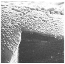
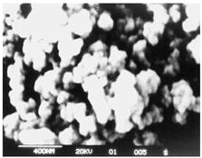
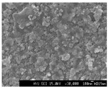
In the synthesis of HgS films on glass and quartz substrates, the authors [38,39,40] and HgSe on glass [49,56] and SnO2/glass [47] reported the formation of spherical particles on the surface at small film thicknesses, corresponding to the initial stage of their growth. With an increase in thickness, the authors observed the development of a dense coating with a smooth surface, resulting from the aggregation of spherical particles. The authors [40] noted that particle size depends on the [Complex-former]: [Hg2+] concentration ratio and the synthesis temperature. Additionally, [41,42] reported that the surface of HgS films synthesized on FTO/glass substrates and HgSe on glass substrates, SnO2/glass, and polyester [44,45,46] consists of crystalline grains, the size of which differs from values calculated from the diffraction pattern using the Debye-Scherrer formula. This difference is attributed to the aggregation of smaller grains during the film growth process. Micrograph analysis by the authors [49] revealed clearly defined spherical particles of approximately the same size with a good grain background, indicating single-step growth through multiple nucleation on the substrate’s surface.
In the synthesis of HgSSe films on glass substrates, the authors [51] observed the formation of highly oriented columnar disks with a size of 100 nm and a thickness of 6 nm, The authors [57] obtained HgSSe films with a solid, smooth, and uniform surface, revealing only a small amount of precipitate and irregular-shaped defects.
3.1. Influence of Substrate Nature and Its Pre-Treatment
In the majority of studies, glass and its modifications (FTO/glass, SnO2/glass, PbS/glass) are employed as model substrates, with additional use of substrates made of polyester, quartz, and plexiglass. Despite their diverse crystalline structures, most cases exhibit the formation of HgS, HgSe, and HgSSe films with a cubic structure [39,42,44,45,47,48,49,51,54,55,56,57]. Furthermore, authors [40,46] report the synthesis of polycrystalline films, whose structure is challenging to determine due to the presence of numerous broad peaks in the diffraction pattern with approximately equal intensity.
Authors [43] achieved films on PbS/glass substrates with predominant α-phase and γ-phase impurities in HgS, while authors [50] obtained amorphous HgSe films. The stoichiometry of Hg:X (where X is S, Se) in the films is 1:1, except for [42], where it is 36:63%; [49] – 1:0.969; and [51,57], where the authors synthesized a solid solution with HgSSe substitution, with the ratio of Hg:S:Se being 1:0.52:0.48 [51] or ranging from 1.0:0.93:0.07 to 1.0:0.67:0.33 [57]. In a follow-up investigation of the same sample four months later, the authors did not observe any changes.
In a study by authors [38], it was noted that using plexiglass as a substrate for HgS synthesis resulted in a narrower absorption maximum range compared to glass substrates. In another study [39], the surface of glass substrates was modified by applying 3-mercaptopropyltrimethoxysilane, which bound Hg2+ using the thiol groups (–SH) present in its structure. During subsequent thermal decomposition, organic compounds broke down to form HgS films without its formation in the solution, ensuring the most efficient utilization of the reagents.
In the synthesis of HgSe films on SnO2/glass substrates, authors [45] suggest that the pre-deposited SnO2 film acts as nucleation centers for the condensation of HgSe, serving as a catalyst for further film growth. Authors [47,49] reported that in the presence of a SnO2 film, the induction period for film formation is reduced. In a study by authors [47], films were also synthesized on glass substrates without prior deposition of SnO2, resulting in broader peaks of lower intensity on the diffraction patterns, indicating a decrease in the crystallinity of the films. According to their statement, film growth occurs more easily on substrates with a similar structure because the nucleation-free energy is then not significant.
Authors [46,48,49] conducted synthesis on glass substrates, the surface of which was previously activated by exposure to hydrochloric acid [46] or chromic acids [48,49], resulting in stronger adhesion of the films to the substrate surface. Authors [49] claimed that film growth on activated substrates begins due to the absorption of Hg2+ ions on the substrate surface, which interact with halogen ions, forming primary nucleation centers.
During the synthesis of HgSe films on polyester, authors [44] observed surface cracking of the films when their thickness exceeded 2 μm, creating certain difficulties in the development of flexible solar cells. They also considered cluster growth mechanisms to be the primary mode, although they did not exclude the possibility of ion-ion growth mechanisms at the final stage of growth due to the depletion of the working solution.
3.2. Influence of the Working Solution Temperature and Annealing Conditions
Temperature is a crucial parameter in the CD method, significantly impacting the rate of sulfide ion release and the dissociation of mercury ions from their complexes. This, in turn, accelerates the formation rate of mercury chalcogenides. In the reviewed literature, the investigation of the synthesis temperature’s impact on film properties was carried out by authors [38,40,41,52,54], while the influence of annealing was studied by [39,44,46,47,49].
A substantial number of works focus on the synthesis of mercury chalcogenide films at temperatures ranging from 0 to 40 ℃ [38,42,44,45,47,48,49,50,51,54,56], whereas fewer studies concentrate on synthesis at temperatures from 60 to 90 ℃ [39,43,46,52,53,55,57]. Authors [47,49,51] additionally conducted reagent mixing at 5 ℃ with a subsequent temperature increase to room temperature over several hours. According to the authors, the use of low temperatures during mercury chalcogenide film synthesis is essential to slow down the release of sulfide ions and the dissociation of mercury ions from their complexes. Authors [49] also highlight that conducting synthesis at low temperatures allows for avoiding diffusion along the grain boundary, resulting in films with a better stoichiometric ratio of components and fewer packing defects.
At a synthesis temperature of up to 25 °C in an alkaline medium using iodine (I-) ions as a complexing agent, authors [38] observed the formation of dense HgS films on dielectric substrates. These films consisted of spherical particles of approximately the same size, resulting in a smooth surface. However, at higher temperatures, non-uniform film growth was noted, with significant variations in crystal sizes. The authors attribute this behavior to the temperature’s influence on key parameters such as the diffusion rate of ions in the solution (directly proportional to temperature), coagulation (inversely proportional as reagents get depleted), and adsorption-desorption of colloids on growing layers. These parameters also depend on the concentration of reagents in the working solution, introducing variability in the results based on the chosen conditions. In the case of synthesizing HgSe films at 20 °C using I- ions, the authors [55] observed the formation of coatings consisting mostly of the undesired ternary compound Hg3I2Se2. However, they were able to obtain single-phase HgSe films with a solid and homogeneous surface when the synthesis was carried out at 90 °C. It was noted that side processes may occur at lower temperatures based on the interaction between HgSe and [HgI4]2- complex ions, which leads to the formation of Hg3I2Se2.
Authors [40] observed a direct proportionality between the synthesis temperature and the size of crystalline grains, film thickness, and growth rate of the films. Simultaneously, they noted an inverse proportionality with electrical resistance and the value of Eg. Interestingly, it was found that the value of Eg decreases with an increase in grain size up to 8 nm. Beyond this point, further increases in grain size result in negligible changes in Eg. This influence on Eg is attributed to the quantum size effect, where in microcrystalline thin films, the quantization of free carriers directly depends on the sizes of crystalline grains.
The reduction in grain size is attributed to a decrease in the dissociation degree of the reactants (mercury complex and Na2S2O3) or a noticeable slowing down of it. The inverse dependence of film resistance on temperature is explained by a reduction in packing defects during film growth at lower synthesis temperatures. This is because, at lower temperatures, smaller grains are formed, and the lower growth rate results in thinner films. Consequently, the resistance is inversely proportional to both the thickness of the films and the size of the crystalline grains. Additionally, authors [47] emphasize that the film growth rate is influenced by the concentration of components and the pH of the working solution.
In the study [41] authors observed that as the synthesis temperature increases from 0 to 85 °C, the thickness of the films increases from 51 to 181.5 nm. Simultaneously, the spectral response for films within this thickness range shifts towards longer wavelengths (λ), specifically from 510 to 570 nm. This shift is explained by the increase in the film’s thickness and the size of the crystalline grains. During the synthesis of HgSe films, authors [45] noted that as the synthesis temperature increases, the maximum film thickness, synthesized in the same amount of time, increases up to a certain temperature. Beyond that point, it either remains the same or decreases due to the rapid exhaustion of reagents and partial dissolution of the upper film layer. Additionally, authors [47,49] found that when mixing reagents at a temperature of 5°C to achieve the maximum thickness of HgSe films, the optimal heating rate of the working solution is 5°C per hour.
Considering the aforementioned findings, it can be inferred that the structure of the synthesized films is contingent on the temperature. Specifically, films with a cubic structure were obtained at low synthesis temperatures, while at higher temperatures, a mixture of modifications [43] or films with a challenging-to-determine crystalline structure [40,46] were produced.
In investigations into the influence of annealing conditions, authors [39,44,46,47,49] observed a decrease in the width of characteristic reflections on the diffraction patterns of annealed samples, a slight increase in their relative intensity, and no changes in the crystalline structure. Additionally, they noted an increase in the size of the crystalline grains, signifying an improvement in the crystallinity of the films.
While investigating the optical properties of annealed samples, authors [44,46] noted a shift in the absorption edge towards shorter wavelengths (λ) and a reduction in the value of Eg. Specifically, authors [46] found that as the annealing temperature increases, there is a shift in the absorption edge towards shorter wavelengths (λ). Moreover, with increasing annealing time at a constant temperature, the value of Eg increases. The authors concluded that the annealing temperature is directly proportional to the absorbance capacity of the films but inversely proportional to the width of the bandgap. In simpler terms, annealing enhances the reorganization of the films, promotes the evaporation of absorbed water, reduces the number of defects by filling voids in the film, increases grain size, and consequently decreases the width of the bandgap. However, authors [39] found an anomalously high value of Eg (3.2 eV) and attributed it to the presence of very small-sized crystalline grains (16 nm).
3.3. Influence of Deposition Duration
Table 1 presents a diverse range of deposition times for the synthesis of mercury sulfide films, spanning from 0.5 min to 75 h, and for mercury selenide films, varying from 2 min to 7 h. In the context of industrial production, extended synthesis periods are energy-intensive. Hence, selecting the optimal deposition time becomes a crucial step in establishing an economically viable method for the industrial production of solar cells based on mercury chalcogenides. It’s important to note that the pH of the solution undergoes changes during synthesis. In prolonged synthesis, the use of buffers becomes necessary to stabilize it, adding to the production cost.
All authors consistently observe that with an increase in deposition time at low temperatures, both the film thickness and the size of the crystalline grains increase. Simultaneously, the values of Eg, specific resistance, and light transmittance of the films decrease. In the case of synthesis at high temperatures, authors [45] note that the maximum film thickness, synthesized within the same time frame, increases up to a certain temperature. Beyond this point, the thickness either remains unchanged or decreases due to the rapid depletion of reagents and partial dissolution of the upper layer of the film.
3.4. Influence of the Choice of Initial Reagents and Their Concentration
The dependence of the reaction rate on concentration is directly proportional, indicating that an increase in the concentration of the initial reagents results in an increased reaction rate. Therefore, it is not advisable to conduct synthesis from concentrated solutions, as metal ions become challenging to control in terms of their content in the working solution, leading to a higher reaction rate. However, if the stability constant of the complex is proportional to or greater than the product of the metal chalcogenide’s solubility, the formation of the complex will not occur. On the contrary, if the product of solubility is significantly larger than the stability constant of the complex, using the complexant would be impractical, as the concentration of uncomplexed metal ions would be sufficient for compound formation. An exception might arise when the source of halide ions is a complex reagent. In this case, the formation of the metal halide occurs due to a change in the pH of the working solution, leading to the hydrolysis of the complex with the formation of the metal halide.
For the synthesis of HgS, HgSe, and HgSSe films, various mercury salts were employed as the source of mercury ions. These included mercury acetate [39,42], mercury nitrate [43,44,47,49,51,52,53,54,55,56,57], mercury chloride [38,40,41,45,46], and HgO [48,50]. Authors utilized diverse complexing agents such as ammonia [44,47,49,51], ammonium citrate [45], iodide [38,55], triethanolamine (TEA) [42,46] formamide [48,50], sodium thiosulfate [54], potassium thiocyanate [56] and thiourea [52,53,57]. Chalcogenizing reagents consisted of sodium sulfide [38], thiourea [38,42,52], sodium thiosulfate [40,41,43,51], sodium selenosulfate [44,45,46,47,48,49,50,54,55,56], a mixture of sodium thiosulfate and sodium selenosulfate [51], and a mixture of thiourea and sodium selenosulfate [57].
The synthesis conditions were maintained at different pH levels of the working solution, namely 2-3 [41], 5.74-7.12 [52], 7.1 [53], 7.02-7.20 [57], 8 [42], 8.51-8.68 [54], 9 [49], 9.5 [55], 9.8 [56], 10 [44,47], 10.5 [45,48,51], and 11 [43,50]. Authors [38] also investigated the influence of the ratio on the optical properties of the films in the pH range from 2 to 12. To achieve the desired pH value, NH3 [42,43,45,46] or NaOH [38,50,51] was used. Notably, the authors did not observe a significant influence of the nature of the starting mercury salt on the properties of the synthesized films.
The authors [38] observed that, in the absence of a complexing agent, HgS films do not form at Hg2+ concentrations less than 10-3 mol/L when using Na2S. In their studies on the influence of the molar ratio on the light absorption spectra using thiocarbamide, they found that absorption increases with an elevated concentration of the mercury iodide complex, reaching its maximum value at k = 3. They also established a direct relationship between synthesis time and reagent concentration, indicating that higher reagent concentrations require more time to achieve films with the same degree of surface roughness. Reagent concentrations also influence processes such as diffusion, coagulation, and adsorption-desorption of colloids on the growing layers.
The authors [39] employed a layer-by-layer self-organization method to synthesize HgS films, followed by annealing at 230 ℃. Substrates, pre-coated with 3-mercaptopropyltrimethoxysilane, were sequentially immersed in alcohol solutions of mercury acetate and 1,6-hexanedithiol for specific durations, with rinsing between each immersion. Upon annealing these multilayers, they obtained a dense film with a cubic structure, devoid of impurities from other phases, and exhibiting good adhesion to the substrate surface. The size of crystalline grains and the morphology of the films were found to depend on the duration of substrate immersion.
In [48] and [50], authors synthesized HgSe films using the same reagents, with the distinction that in [50], polyvinylpropylene was added to the working solution. The structure of the HgSe films in [48] is cubic, while in [50], it is amorphous. Moreover, better adhesion is observed when using polyvinylpropylene as a substrate. This suggests that the viscosity of the solution can influence the properties of the synthesized coatings.
Stirring the solution promotes uniform reactant concentrations, increases the rate of formation of sparingly soluble compounds, and allows for the production of homogeneous films from concentrated solutions. The authors determined that the optimal stirring rate is 80 ± 2 RPM [45].
4. Electrical and Optical Properties
The authors investigated the optical and thermoelectric properties of the films [39,40,41,42,43,44,47,49,50,51]. As mentioned earlier, the electrical resistance of the films is inversely proportional to their thickness and the size of crystalline grains. Therefore, it exhibits a similar dependence on factors such as synthesis temperature and reagent concentration [40], annealing temperature [44], and synthesis time. However, at high concentrations of reacting components, the number of packing defects increases due to the rapid growth rate of the films, leading to an increase in the electrical resistance of the films [40].
The authors [39,41,42] observed a decrease in electrical resistance when exposed to light, confirming their photosensitivity. The electrical resistance values for HgS films varied in the range of 103 to 104 ohms [39,40]. However, the authors [41] reported a resistance value in the range of 107 to 108 ohms, which they attributed to the small thickness of the synthesized films (51 nm). Authors [43] obtained a resistance value of 1 × 10⁹ ohms for films with a thickness of 80 nm, and for conducting studies, the films were immersed in a silver ammonia solution .
For HgSe films, the electrical resistance values were in the order of 103 Ω [45,47,49]. Authors [44] found resistance values for freshly deposited HgSe films to be around 105 ohms. After annealing the films, their resistance decreased by an order of magnitude, and this dependence was irreversible. With annealing durations of less than one hour, the resistance practically did not change. For films of the solid solution HgSSe, authors [51] reported resistance values of around 103 Ω for films with a thickness of 710 nm.
Based on thermoelectric studies in the temperature range of 300-500 K in the dark, authors [42] determined p-type conductivity for HgS and HgSe films [50]. For HgSe [45,47,49] and HgSSe [51], n-type conductivity was observed. Additionally, during the investigation of the temperature influence on conductivity, authors [40,45] recorded a direct proportional dependence, confirming the semiconductor nature. The activation energy (Ea) for the conductivity of HgSe films was found to be 0.05 eV [45], and 0.11 eV [47,49]. Authors [50,51] observed two conductivity regions: low-temperature and high-temperature, while Ea for the low-temperature range was 0.114 eV [51], and for the high-temperature range, it was 0.71 eV [50] and 0.374 eV [51].
Authors [41] note a significant deviation of the ideality factor (n) function from the ideal value when investigating optoelectronic properties. The difference in n‘‘ under light exposure is explained by an increase in charge transfer through the semiconductor-electrolyte interface, with a significant contribution from the recombination of surface states and deep traps. Short-circuit current and open-circuit voltage, and thus the conversion efficiency, increase with the thickness of the films. Authors [42] determined a photoelectric output of 0.34% with a fill factor of 34%. According to them, the low efficiency is associated with a high series resistance and low shunt resistance of the cell and interface, corresponding to the recombination mechanism.
Investigations into the optical properties of mercury chalcogenide films were conducted by the authors [39,40,41,42,43,44,45,46,47,48,49,50,51,52,53,54,55,56,57]. The absorption coefficient values for HgSe films were reported as 103 cm-1 [45] and 104 cm-1 [48,49]. During the investigation of light transmission [40,43,46,48,52,53,54,55,57] and absorption spectra [39,42,44,45,47,49,50,51,56] for mercury chalcogenide films, it was observed that with an increase in their thickness, the transmission decreases [43,44,48,52,54,55], and light absorption increases [44,46,56].
For HgS films, the spectral response was localized in the wavelength range λ: 350 – 400 nm [39,52]; 550 – 650 nm [40]; 475 – 550 nm [41,42]; 400 – 500 nm [43,53]. The authors [40] noted that with an increase in the synthesis temperature, there is a shift in the spectral response towards longer wavelengths λ: 650 – 750 nm. The authors [41] observed a similar change with an increase in film thickness.
For HgSe films, light absorption sharply decreased in the wavelength range λ: 500 – 600 nm [44]; 1550 nm [45]; 280 – 330 nm [46]; 1300 – 1600 nm [47,49]; 1250 – 1750 nm [48], and for HgSSe films [51,57]: 350 – 550 nm. The authors [44,48,49] also observed a similar change in the spectral response with an increase in film thickness. Moreover, the authors [44,48] established a direct proportionality between the annealing temperature and light absorption, and a shift of its maximum towards longer wavelengths, which they interpret as an increase in the size of crystalline grains.
The light reflection coefficient, according to the results of the study [46], is inversely proportional to the annealing temperature. The authors [48] found that with an increase in film thickness, optical transmission decreases proportionally to the wavelength λ, and in the range of 1500-2000 nm, it increases because the reflective ability decreases.
For HgS films, the values of Eg were reported as follows: 3.2 eV [39]; 2.0 – 2.4 eV [40]; 2.75 eV [42]; 3.1 eV [43]; 2.84 – 3.20 eV [52]; and 1.78 – 2.86 eV [53]. Regarding HgSe films, the reported values were 2.5 eV [44]; 0.81 and 0.45 eV [45,47,49]; 1.06 – 1.72 eV [46]; 0.84 eV [48]; 1.42 eV [50]; 1.39 – 2.47 eV [54]; 2.05 – 2.90 eV [55]; and 2.40 – 3.05 eV [56]. For HgSSe films, the reported values were 2.1 eV [51] and 2.43 – 2.70 eV [57].
The authors [39,44] explained these Eg values in terms of the influence of annealing temperature and crystalline grain size. Additionally, the authors [44,51], citing the results of other researchers, indicated an Eg value of 3.15 eV for colloidal particles with a size of 2-3 nm. The authors [51] reported Eg values for HgSe films with a crystalline structure and particle size of ≈8 nm: 2.5 eV; for films with particle size 30 nm – 0.8 eV and 0.88 eV for crystalline grain size ≈42 nm. The variation in Eg values for mercury selenide films is attributed to the large excitonic Bohr radius. In the case of amorphous HgSe films, Eg was found to be 1.42 eV [50].
It is noteworthy that both negative and positive values of Eg have been reported in the literature for HgS films. The absorption edge shifted from the near-infrared to the ultraviolet-visible region for HgS films with a particle size of ≈13 nm. For β-HgS nanoparticles with a particle size of ≈15 nm, Eg was 1.38 eV, and for particles with a size of 10 nm, it was 2.6 eV.
Authors [40] also noted a correlation between Eg and the size of crystalline grains, highlighting its dependence on synthesis temperature. In their study, authors [43] observed increased light absorption in HgS films with silver ammonium doping, and this absorption rose with extended doping time. However, the authors [52,54] determined that increasing the thickness during growth results in a decrease in Eg. Similarly, authors [53] observed the same tendency with increasing numbers of film layers. Additionally, authors [46] reported a proportional relationship between Eg and annealing duration, in addition to its inverse correlation with annealing temperature.
When plotting the graph using the coordinates (αhν)n – hν to determine Eg at n = ½ and n = 2, authors [44,45,47,49] observed similar graphical dependencies. These dependencies correspond to direct allowed (n = ½) and indirect forbidden (n = 2) transitions. The direct transition results from the spin-orbital splitting of the valence band to the conduction band, while the indirect transition occurs through the transition from a virtual state in the valence band to the conduction band minimum [44,45].
5. Conclusions
A literature review has been conducted to identify optimal conditions for synthesizing mercury sulfide and mercury selenide films using the chemical deposition method. The analysis covers the physical and optical properties of the films, their surface morphology, and phase composition. Dependencies of the films’ physical properties on various factors have been established, including the nature and concentration of substances, temperature, viscosity of the working solution, deposition duration, the nature of the substrate, its pre-treatment or modification, and annealing conditions.
Despite the abundance of experimental data, the synthesis of films often relies on a recipe-experimental approach, with fixed or poorly studied synthesis conditions. The chemical deposition method was chosen for the synthesis of HgS and HgSe films based on this analysis. This method stands out for its simplicity, cost-effectiveness, and the absence of a requirement for expensive equipment or special synthesis conditions. While the utilization of HgS and HgSe films may be limited due to their complex preparation, materials derived from these films – whether doped with other elements or combined with layers of mercury sulfide and mercury selenide films, or other semiconductor materials – hold promise for unique properties. These materials find applications or have the potential to enhance the performance of various electronic and optical devices.
The study emphasizes the significance of creating new semiconductor materials and modifying existing ones as a current scientific challenge. Thus, further research in this direction is essential for a comprehensive understanding of how different factors influence the properties of chemically deposited HgS and HgSe films. Additionally, exploring the possibility of synthesizing these films with predetermined functional properties is crucial for developing new thin-film semiconductor materials and enhancing existing materials based on them.
Author Contributions
Conceptualization, V.S. and R.G.; methodology, V.S., and P.S.; software, M.S.; validation, L.D., P.S., and R.G.; formal analysis, M.S.; investigation, V.S.; resources, V.S. and P.S.; data curation, L.D.; writing—original draft preparation, R.G., and V.S; writing—review and editing, M.S.; visualization, L.D.; supervision, P.S.; project administration, R.G. All authors have read and agreed to the published version of the manuscript.
Funding
This research received no external funding.
Institutional Review Board Statement
Not applicable.
Informed Consent Statement
Not applicable.
Data Availability Statement
Data supporting reported results are stored by R. Guminilovych.
Conflicts of Interest
The authors declare no conflicts of interest.
References
- Sharma, R.C.; Chang, Y.A.; Guminski, C. The Hg-S (Mercury-Sulfur) system. JPE 1993, 14, 100–109. [Google Scholar] [CrossRef]
- Sorokin, V.I.; Boksha, S.S.; Ushakovskaya, T.V. P-T phase diagram of HgS. Geokhimia 1984, 1, 132–136. [Google Scholar]
- Tauson, V.L.; Abramovich, M.G. Investigation of System ZnS-HgS by Hydrothermal Method. Geokhimia 1980, 6, 808–820. [Google Scholar]
- Huang, T.L.; Ruoff, A.L. High-pressure-induced phase transitions of mercury chalcogenides. Phys. Rev. B 1985, 31, 5976–5983. [Google Scholar] [CrossRef]
- Potter, R.W., II; Barnes, H.L. Phase Relations in the Binary Hg-S. Am. Mineral. 1978, 63, 1143–1152. [Google Scholar]
- Sharma, R.C.; Chang, Y.A.; Guminski, C. The Hg-Se (Mercury-Selenium) system. JPE 1992, 13, 663–671. [Google Scholar] [CrossRef]
- Leute, V.; KÖller, H.J. The four quasibinary phase diagrams of the quasitemary system (Hg,Pb)-(Se,Te). Z. Phys. Chem. NeueFolge 1986, 149, 213–227. [Google Scholar] [CrossRef]
- Mariano, A.N.; Varekois, E.P. High-pressure phases of some compounds of groups II-VI. Science 1963, 142, 672–673. [Google Scholar] [CrossRef]
- Huang, T.; Ruoff, A.L. Pressure-induced phase transition of HgSe. Phys. Rev. B 1983, 27, 7811–7812. [Google Scholar] [CrossRef]
- Varshney, D.; Shriya, S.; Khenata, R. Structural phase transition and elastic properties of mercury chalcogenides. Mater. Chem. Phys. 2012, 135, 365–384. [Google Scholar] [CrossRef]
- Pawar, A.R.; Kendre, D.R.; Pujari, V.B. Electrical transport and spectral response of HgZnS thin films. IJAEEE 2013, 2, 68–73. [Google Scholar]
- Pawar, A.R.; Kendre, D.R.; Pujari, V.B. Structural and microscopic studies on mercury zinc sulfide thin films. Journal of Shivaji University 2015, 41, 1–3. [Google Scholar]
- McCann, J.F.; Kainthla, R.C.; Skyllas-Kazacos, M. Chemical deposition of Cd1-xHgxS thin film electrodus for liquid-junction solar cell. Solar Energy Materials 1983, 9, 247–251. [Google Scholar] [CrossRef]
- Garadkar, K.M.; Hankare, P.P.; Patil, P.K. Effect of indium doping on structural, optical and electrical properties of Cd0.95Hg0.05S thin films. Materials Chemistry and Physics 1999, 58, 64–70. [Google Scholar] [CrossRef]
- Skyllas-Kazacos, M.; McCann, J.F.; Arruzza, R. Chemically deposited alloy semiconductor thin films. Applications of Surface Science 1985, 22-23, 1091–1097. [Google Scholar] [CrossRef]
- Deshmukh, L.P.; Garadkar, K.M.; Sutrave, D.S. Studies on solution grown HgхCd1-хS thin films. Materials Chemistry and Physiсs 1998, 55, 30–35. [Google Scholar] [CrossRef]
- Sharma, N.C.; Pandya, D.K.; Sehgal, H.K.; Chopra, K.L. Solution growth of variable gap Pbl-xHgxS films for infrared detectors. Mat. Res. Bull. 1976, 11, 1109–1114. [Google Scholar] [CrossRef]
- Jain, M. Band-gap variation in ternary alloy films. Philosophical Magazine Letters 1988, 58, 59–62. [Google Scholar] [CrossRef]
- Chattarki, A.N.; Maldar, N.N.; Deshmukh, L.P. Synthesis, structure and spectro-microscopic studies of polycrystalline HgxPb1-xS thin films grown by a chemical route. Journal of Alloys and Compounds 2014, 597, 223–229. [Google Scholar] [CrossRef]
- Dappadwad, U.R.; Lande, M.K.; Chonde, S.G.; Arbad, B.R.; Hankare, P.P.; Bhuse, V.M. Synthesis and characterization of Zn0.5Hg0.5Se thin films. Materials Chemistry and Physics 2008, 112, 941–944. [Google Scholar] [CrossRef]
- Bhuse, V.M. Chemical bath deposition of Hg doped CdSe thin films and their characterization. Materials Chemistry and Physics 2005, 91, 60–66. [Google Scholar] [CrossRef]
- Hankare, P.P.; Bhuse, V.M.; Garadkar, K.M.; Delekar, S.D.; Bhagat, P.R. CdHgSe thin films: preparation, characterization and optoelectronic studies. Semicond. Sci. Technol. 2004, 19, 277–284. [Google Scholar] [CrossRef]
- Bhuse, V.M. Photo-electrochemical properties of Cd1−xHgxSe thin films. Materials Chemistry and Physics 2007, 106, 250–255. [Google Scholar] [CrossRef]
- Bhuse, V.M.; Hankare, P.P.; Sonandkar, S. Structural, optical, electrical and photo-electrochemical studies on indium doped Cd0.6Hg0.4Se thin films. Materials Chemistry and Physics 2007, 101, 303–309. [Google Scholar] [CrossRef]
- Pujari, V.B.; Gaikwad, V.B.; Masumdar, E.U.; More, P.D.; Deshmukh, L.P. Chemically synthesized (Cd,Hg)Se pseudobina-ries: some characteristic properties. Turk. J. Phys. 2002, 26, 407–413. [Google Scholar]
- Siemsen, K.J.; Riccius, H.D. Preparation and optical properties of evaporated β-HgS films. Physica Status Solidi (b) 1970, 37, 445–451. [Google Scholar] [CrossRef]
- Nakada, T. Optical absorption and dispersion in rf-sputtered α-HgS films. J. Appl. Phys. 1975, 46, 4857–4861. [Google Scholar] [CrossRef]
- Herbert, K.; Sidney, G.P.; James, P.S. CdxHg1-хTe films by cathodic sputtering. J. Electrochem. Soc.: Solid State Science 1967, 114, 616–619. [Google Scholar]
- Nakada, T.; Kunioka, A. Growth and properties of sputter-deposited α-HgS films in Hg vapor. Jpn. J. Appl. Phys. 1980, 19, 845–848. [Google Scholar] [CrossRef]
- Reynolds, R.A. The II-VI compounds: 30 years of history and the potential for the next 30 years. J. Vac. Sci. Technol. A 1989, 7, 269–270. [Google Scholar] [CrossRef]
- Gichuhi, A.; Edward Boone, B.; Shannon, C. Electrosynthesized CdS/HgS Heterojunctions. Langmuir 1999, 15, 763–766. [Google Scholar] [CrossRef]
- Patel, B.K.; Rath, S.; Sarangi, S.N.; Sahu, S.N. HgS nanoparticles: Structure and optical properties. Applied Physics A. [CrossRef]
- Mahalingam, T.; Kathalingam, A.; Sanjeeviraja, C.; Chandramohan, R.; Chu, J.P.; Kim, Y.D.; Velumani, S. Electrodeposition and characterization of HgSe thin films. Materials Characterization 2007, 58, 735–739. [Google Scholar] [CrossRef]
- Caveney, R.J. Epitaxial growth of II–VI compounds. Journal of Crystal Growth 1968, 2, 85–90. [Google Scholar] [CrossRef]
- Jung, Y.C.; An, S.Y.; Suh, S.H.; Choi, D.K.; Kim, J.S. Ammonium sulfide treatment of HgCdTe substrate and its effects on electrical properties of ZnS/HgCdTe heterostructure. Thin Solid Films 2005, 483, 407–410. [Google Scholar] [CrossRef]
- Suh, S.-H.; Kim, J.-S.; Kim, H.J.; Song, J.-H. Control of hillock formation during MOVPE growth of HgCdTe by suppressing the pre-reaction of the Cd precursor with Hg. Journal of Crystal Growth 2002, 236, 119–124. [Google Scholar] [CrossRef]
- Rao, A.R.; Dutta, V. Nanotubes in spray deposited nanocrystalline HgTe:I thin films. Mater. Res. Soc. Symp. Proc. 2006, 901E, 0901-Ra11-19-Rb11-19.1–0901-Ra11-19-Rb11-19.6. [Google Scholar] [CrossRef]
- Perakh, M. Ginsburg, H. Deposition of thin film of HgS from colloidal solution. Thin solid films 1978, 52, 195–202. [Google Scholar] [CrossRef]
- Mu, J.; Zhang, Y.; Wang, Y. Growth and Characterization of β-HgS Thin Films by Annealing Hg2+-Dithiol Self-Assembled Multilayers. Journal of Dispersion Science and Technology 2005, 6, 641–644. [Google Scholar] [CrossRef]
- Kale, S.; Lokhande, C. Preparation and characterization of HgS films by chemical deposition. Materials Chemistry and Physics 1999, 59, 242–246. [Google Scholar] [CrossRef]
- Kale, S.S.; Pathan, H.M.; Lokhande, C.D. Thickness dependent photo-electrochemical cells performance of CdSe and HgS thin films. Journal of materials science 2005, 40, 2635–2637. [Google Scholar] [CrossRef]
- Patil, R.S.; Gujar, T.P.; Lokhande, C.D.; Mane, R.S.; Han, S.-H. Photoelectrochemical studies of chemically deposited nanocrystalline p-type HgS thin films. Solar Energy 2007, 81, 648–652. [Google Scholar] [CrossRef]
- Najdoski, M.Z.; Grozdanov, I.S.; Dey, S.K.; Siracevska, B.B. Chemical bath deposition of mercury(II) sulfide thin layers. J. Mater. Chem. 1998, 8, 2213–2215. [Google Scholar] [CrossRef]
- Pejova, B.B.; Najdoski, M.Ž.; Grozdanov, I.S.; Dey, S.K. Chemical bath deposition of {111} textured mercury(II) selenide thin layers on transparent polyester sheets. J. Mater. Chem. 1999, 9, 2889–2892. [Google Scholar] [CrossRef]
- Hankare, P.P.; Bhuse, V.M.; Garadkar, K.M.; Jadhav, A.D. A novel method to grow polycrystalline HgSe thin film. J. Mater. Chem. 2001, 71, 53–57. [Google Scholar] [CrossRef]
- Ishiwu, S.M.U.; Nnabuchi, M.N. Studies on growth and characterizatio of mercury selenide thin films prepared by chemical bath technique. Journal of Ovonic Research 2011, 7, 9–14. [Google Scholar]
- Hankare, P.P.; Bhuse, V.M.; Garadkar, K.M.; Delekar, S.D.; Mulla, I.S. Low temperature route to grow polycrystalline cadmium selenide and mercury selenide thin films. Materials Chemistry and Physics 2003, 82, 711–717. [Google Scholar] [CrossRef]
- Girgis, S.Y.; Salem, A.M.; Selim, M.S. Structural characterization and refractive index dispersion analysis of HgSe thin films grown by reactive solutions. J. Phys.: Condens. Matter 2007, 19, 116213–11. [Google Scholar] [CrossRef]
- Hankare, P.P.; Bhuse, V.M.; Garadkar, K.M.; Delekar, S.D.; Mulla, I.S. Chemical deposition of cubic CdSe and HgSe thin films and their characterization. Semicond. Sci. Technol. 2003, 19, 70–75. [Google Scholar] [CrossRef]
- Pramanik, P.; Bhattacharya, S. Deposition of amorphous mercury selenide thin films by aqueous reactive solution growth technique. Mat. Res. Bull. 1989, 24, 945–952. [Google Scholar] [CrossRef]
- Bhuse, V.M. Structural, optical and еlectrical рroperties of nanocrystalline Hg(SSe) semiconductor alloy thin films. Arch. Appl. Sci. Res. 2011, 3, 339–349. [Google Scholar]
- Sozanskyi, M.; Stadnik, V.; Guminilovych, R.; Shapoval, P.; Laruk, M.; Yatchyshyn, Y. , Stadnik, V., Guminilovych, R., Shapoval, P., Laruk, M., Yatchyshyn, Yo. Optimization of synthesis conditions of HgS thin films. Visnyk of the Lviv University. Series Chemistry 2019, 60, 146–154. [Google Scholar] [CrossRef]
- Sozanskyi, M.A.; Siryk, K.M.; Shapoval PYo Huminilovych, R.R.; Stadnik, V.E.; Laruk, M.M. Chemical bath deposition of multilayer HgS films. J. Nano- Electron. Phys. 2023; accepted. [Google Scholar]
- Sozanskyi, M.; Stadnik, V.; Shapoval, P.; Yatchyshyn, I.; Guminilovych, R.; Shapoval, S. Optimization of synthesis conditions of mercury selenide thin films. Chem. Chem. Technol. 2020, 14, 290–296. [Google Scholar] [CrossRef]
- Sozanskyi, M.; Stadnik, V.; Chaykivska, R.; Guminilovych, R.; Shapoval, P.; Yatchyshyn, I. Synthesis and properties of mercury selenide films deposited by using pottasium iodide as complexing agent. Chem. Chem. Technol. 2017, 11, 445–448. [Google Scholar] [CrossRef]
- Sozanskyi, M.A.; Stadnik, V.E.; Chaykivska, R.T.; Shapoval, P.Y.; Yatchyshyn, Y.Y.; Vasylechko, L.O. The effect of different complexing agents on the properties of mercury selenide films deposited from aqueous solutions. Voprosy Khimii i Khimicheskoi Tekhnologii 2018, 4, 69–76. [Google Scholar]
- Sozanskyi, M.A.; Shapoval PYo Stadnik, V.E.; Kyrulo, O.P.; Laruk, M.M. Hydrochemical Synthesis of HgS1–xSex Film Solid Solutions. J. Nano- Electron. Phys. 2021, 13, 05032-1–05032-5. [Google Scholar] [CrossRef]

Table 1.
Synthesis conditions and properties of mercury chalcogenide films.
| Reagents and Synthesis Conditions, Ref. | Surface Morphology | Note |
|---|---|---|
| HgS | ||
| A) By an exchange reaction: HgCl2, Na2S. B) By a reaction involving the formation of intermediate complex compounds: HgCl2; NaI; NaOH; SC(NH2)2; H2O [38]. Conditions: рН > 7; temperature: 7–30 °С; duration: 960 – 1440 min; substrate: glass, plexiglass |
 |
Polycrystalline structure. Film thickness: 35 – 1030 nm |
| Silar (the reagents are provided in the order of their application) followed by the subsequence annealing of self-organized layers. C6H16SSiO3 (3-mercaptopropyltrimethoxysilane); С6H5CH3; (CH3COO)2Hg/C2H5OH; C2H5OH; С6Н14S2 (1,6-hexanethiol)/C2H5OH; C2H5OH [39]. Conditions: рН ≥ 7; synthesis temperature: 90 °С; annealing temperature: 230 °С; synthesis stage duration: 5 min; annealing duration: 120 min; substrate: SiO2 |
Cubic crystal structure (metacinnabar). Film thickness – 195 nm. Eg = 3.2 eV. |
|
| HgCl2, Na2S2O3. Conditions: рН: 2 – 3; temperature: 0 – 85 °С; duration: 45 – 4320 min; substrate: glass [40] |
 |
Polycrystalline structure. Film thickness: 50 – 180 nm. Increasing the synthesis temperature results in a decrease in specific resistance and bandgap width (Eg) |
| HgCl2, Na2S2O3. Conditions: рН: 2 – 3; temperature: 0 – 85 °С; duration: 45 – 4500 min; substrate: Ti [41] |
The film thickness is 51 – 181.5 nm. With an increase in the thickness of the films, the short-circuit current (Isc) and open-circuit voltage (Voc) decrease, while the conversion efficiency (η) increases |
|
| (CH3COO)2Hg, SC(NH2)2, (HOCH2CH2)3N, NH3. Conditions: рН: 8; temperature: 27 °С; duration: 240 min; substrate: glass [42] |
 |
Face-centered cubic crystal structure. Film thickness – 133 nm. Eg = 2.75 eV. p-type conductivity |
| Hg(NO3)2, NH3, Na2S2O3. Conditions: рН: 11; temperature: 65 °С; duration: 5 – 180 min; substrate: glass/PbS [43]. |
A mixture of γ-HgS and the dominant α-HgS. Film thickness: 30 – 500 nm. Eg = 3.1 eV. |
|
| Hg(NO3)2, Na3C6H5O7, (NH2)2CS. Conditions: рН: 5.74-7.12; temperature: 50-90 °С; duration: 0.5-5 min; substrate: glass [52] |
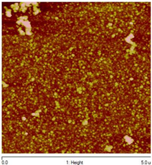 |
The structure is trigonal (cinnabar). Film thickness: 4 – 46 nm. Eg = 2.84 – 3.20 eV. Increasing thickness during the growth results in a Eg decrease. Grain size is around 50 nm. |
| Hg(NO3)2, Na3C6H5O7, (NH2)2CS. Conditions: рН: 7.1; temperature: 90 °С; duration: 5 min; substrate: glass [53] |
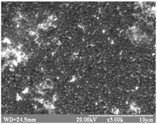 |
The coatings consisted of 1–5-layer HgS films The structure is trigonal (cinnabar). Eg = 2.43 – 2.70 eV. Increasing number of layers results in a Eg decrease. |
| HgSe | ||
| SnCl2, Hg(NO3)2, NH3, Na2SeSO3. Conditions: рН > 7; temperature: 10 °С; duration: 180 min; substrate: polyester [44] |
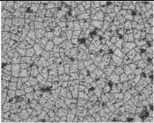 |
Crystal structure – cubic (zinc blende). Film thickness: 27 – 250 nm |
| HgCl2, C6H5O7(NH3)3, NH3, Na2SeSO3. Conditions: рН = 10,5; temperature: 60 °С; duration: 90 min; substrate: glass/SnO2 [45] |
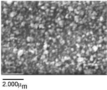 |
Crystal structure – cubic (zinc blende). Film thickness: 230 – 580 nm. Eg = 0.81 еV. The conductivity of the films increases with an increase in temperature |
| HgCl2, NH3, (HOCH2CH2)3N, Na2SeSO3. Conditions: рН > 7; temperature:75 °С; duration: 60 – 105 min; substrate: glass [46] |
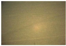 |
Polycrystalline crystal structure. With an increase in annealing temperature, Eg decreases due to a reduction in the number of surface defects and an increase in the size of crystalline grains |
| Hg(NO3)2, NH3, Na2S2O3 Conditions: рН > 7; temperature: 20 °С; duration: 180 min; substrate: glass/SnO2 [47] |
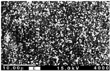 |
The structure – cubic. Film thickness: 25 – 800 nm. Eg = 0.82 eV. n-type conductivity. |
| HgO, NH2CHO, NaOH, Na2SeSO3. Conditions: рН = 10,5; temperature: 27 °С; duration: 120 – 180 min; substrate: glass [48] |
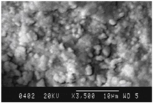 |
The structure – cubic. Film thickness – 418 nm, Eg = 0.84 еV. |
| Hg(NO3)2, NH3, Na2SeSO3, C2H5OH. Conditions: рН = 9; temperature: 20 °С duration: 30 – 420 min; substrate: glass [49]; |
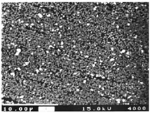 |
Crystal structure – cubic. Film thickness: 80 – 800 nm, Eg = 0.81 еV. n-type conductivity |
| HgO, NH2CHO, NaOH, [С6H9NO]n, Na2SeSO3. Conditions: рН > 7; temperature: 27 °С; duration: 30 – 300 min; substrate: glass [50] |
Wurtzite in structure. Film thickness: 50 – 500 nm. Eg = 1.42 eV. p-type conductivity |
|
| Hg(NO3)2, Na2S2O3, Na2SeSO3., Na3C6H5O7. Conditions: рН: 8.51-8.68; temperature: 0-40 °С; duration: 20-220 min; substrate: glass [54] |
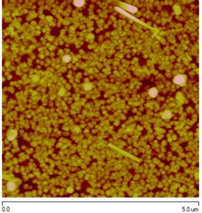 |
The structure is cubic (zinc blende). Film thickness is 10 – 112 nm. Eg = 1.39 – 2.47 eV. Increasing thickness during the growth results in a Eg decrease. Grain size: 15 – 152 nm. |
| Hg(NO3)2, KI, Na2SeSO3. Conditions: рН: 9.5; temperature: 90 °С; duration: 2-10 min; substrate: glass [55] |
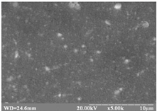 |
The structure is cubic (zinc blende). Eg = 2.05 – 2.90 eV. |
| Hg(NO3)2, KSCN, Na2SeSO3. Conditions: рН: 9.8; temperature: 20 °С; duration: 20-80 min; substrate: glass [56] |
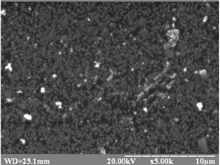 |
The structure is cubic (zinc blende). Eg = 2.40 – 3.05 eV. |
| Hg(SSe) | ||
| Hg(NO3)2, NH3, Na2SeSO3, Na2S2O3, NaOH. Conditions: рН: 10,4; temperature: 27 °С; duration: 180 min; substrate: glass [51] |
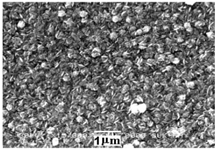 |
Crystal structure – cubic. Film thickness – 710 nm, with the stoichiometric ratio Hg:S:Se = 1.0:0.52:0.48. Eg = 2.1 eV. |
| Hg(NO3)2, Na3C6H5O7, Na2SeSO3, (NH2)2CS. Conditions: рН: 7.02-7.20; temperature: 90 °С; duration: 5 min; substrate: glass [57] |
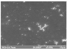 |
The structure changes from a trigonal (cinnabar) to cubic (zinc blende), and the stoichiometric ratio Hg:S:Se varies from 1.0:0.93:0.07 to 1.0:0.67:0.33. Eg = 2.43 – 2.70 eV. |
Disclaimer/Publisher’s Note: The statements, opinions and data contained in all publications are solely those of the individual author(s) and contributor(s) and not of MDPI and/or the editor(s). MDPI and/or the editor(s) disclaim responsibility for any injury to people or property resulting from any ideas, methods, instructions or products referred to in the content. |
© 2023 by the authors. Licensee MDPI, Basel, Switzerland. This article is an open access article distributed under the terms and conditions of the Creative Commons Attribution (CC BY) license (http://creativecommons.org/licenses/by/4.0/).
Copyright: This open access article is published under a Creative Commons CC BY 4.0 license, which permit the free download, distribution, and reuse, provided that the author and preprint are cited in any reuse.