Submitted:
08 August 2023
Posted:
08 August 2023
You are already at the latest version
Abstract
In this paper we present methodology for precise calibration of Molecular Beam Epitaxy (MBE) growth process and achieving run to run stability of growth parameters. We present the analysis of the influence of fluxes stability during the growth of long wavelength quantum cascade laser structures designed for the range λ ~ 12–16 µm on wavelength accuracy with respect to desired emission wavelength. The active region of the lasers has a complex structure of nanometer thickness InxGa1-xAs/InyAl1-yAs superlattice. As a consequence, the compositional and thickness control of the structure via bulk growth parameters is rather difficult. To deal with this problem we employ methodology based on double-superlattice test structures, that precede the growth of the actual structures. The test structures are analyzed by high-resolution X-ray diffraction which allows to calibrate the growth of the complex active region of quantum cascade laser structures. We also study theoretically the effect of individual flux changes on emission wavelength and gain parameters of the laser. The results of simulations allow for determination of flux stability tolerance, preserving acceptable parameters of the laser and provide means of emission wavelength control. The proposed methodology was verified by the growth of laser structures for emission at around 13.5 μm.
Keywords:
quantum cascade laser
; molecular beam epitaxy
; InAlAs/InGaAs
1. Introduction
Quantum Cascade Lasers (QCLs) are of great interest due to the large number of applications in molecular spectroscopy. Among their main advantages are small compact size, stable room temperature operation, reliability and last but not least wavelength tunability. Mid-IR spectroscopy in general provides rapid, label-free and objective analysis, particularly important in the field of environmental studies, industry and biomedical analysis. The quantum cascade lasers used for trace gas sensing applications are mostly based on InxGa1-xAs/InyAl1-yAs/InP structures [1]. Short wavelength devices operating at λ = 4.5–5.5 µm are designed for sensing of carbon dioxide (CO2) and monoxide (CO) and nitride monoxide (NO) and dioxide (NO2) where the strongest absorption lines for these compounds are presents. They are based on strain compensated In0.66Ga0.34As/In0.36Al0.64As/InP structures providing large enough conduction band discontinuity (band offset) required to confine large energy electronic transitions [2]. The lasers operating at λ ~ 9 µm used for ammonia (NH3) detection are mostly made of lattice matched In0.53Ga0.47As/In0.52Al0.48As/InP [3].
In recent years there has been growing interest in devices operating at longer wavelengths in the λ ~ 10–16 µm range [4,5,6]. Here the strongest absorption lines of aromatic hydrocarbons BTEX (benzene, toluene, ethylbenzene, and xylenes) are placed [7]. BTEX are aromatic compounds of similar chemical structure, properties, and behavior in the environment. These compounds are important and widely used solvents and industrial chemicals. As constituents of crude oil they are present in refined petroleum products. The most common sources of exposure to BTEX compounds are from breathing contaminated air, particularly in areas of heavy motor vehicle traffic and petrol stations.
Compared with short-wavelength QCLs, there are a few main challenges for long-wavelength QCLs. First, a large population inversion is more difficult to attain, since the lifetime of the upper laser level drops as the optical transition energy decreases due to a higher longitudinal optical (LO) photon scattering rate. Second, the leakage from the injector directly to the lower laser level is for the same reason high. And finally, the waveguide losses due to free-carrier absorption which are proportional to the square of the wavelength are high. As a consequence long-wavelength QCLs reported so far have a high threshold current density and low output power comparing to QCLs emitting in the λ ~ 4.5–10.0 μm range.
In spite of notable accomplishments, the epitaxial growth of QCL structures continues to be a challenge. In particular, for complex ternary systems, the requirements for the precise control of its composition, layer thickness, and interface quality make the heterogeneous epitaxial growth of InP-based QCL structures very challenging [8,9,10]. However, the current QCL literature focuses on the performance aspects of devices, with little works devoted to growth methodology. In particular, the emission wavelength necessary to obtain the required sensitivity of detection systems is still difficult to control. In this paper we present methodology for precise calibration of MBE growth process and achieving run to run stability of growth parameters.
2. Materials and Methods
The growth was performed by solid source MBE using Riber Compact 21T epitaxial reactor, equipped with double Ga, In and Al group III sources placed in ABN80DF double zone effusion cells. The As group V material was placed in VAC500 valved cracker effusion cell. The n-type dopant necessary for electrical conduction of the structures was Si placed in single zone effusion cell ABN135L. The growth process was controlled by in situ Reflection High Energy Electron Diffraction (RHEED), LayTec-EpiTT optical reflectance observation and mass spectrometer residual gas analyzer. The process temperature was controlled by optical pyrometer Modline 3, calibrated at the temperature of oxide desorption from epi-ready GaAs substrate equal 582 °C [11]. After growth process samples surfaces were inspected by optical microscope Olympus DSX. The structural parameters and quality of heterostructures were investigated by High Resolution X-Ray Diffraction (HRXRD) technique. The measurements were performed on the Panalytical X’Pert PRO MRD diffractometer equipped with X-ray source (XRD Empyrean tube), four bounce Ge (400) hybrid monochromator, four-circle cradle, three bounce Ge (220) analyzer and two detectors: proportional and Pixcel. The diffraction curves and reciprocal lattice space maps of investigated structures were collected in Triple Axis geometry.
The studied long wavelength (λ > 13 μm) lasers were based on In0.533Ga0.467As/In0.522Al0.478As material system, lattice-matched to the InP substrate. The active region was based on diagonal transition and three-phonon-resonance design. The layer sequence of one period of the structure, in nanometers, was: 4.1 (Injection Barrier (IB)), 3.1, 0.8, 4.6, 0.8, 5.4, 0.7, 5.5, 0.8, 4.6, 2.1 (Extraction Barrier (EB), 4.0, 1.0, 3.5, 1.6, 3.6, 2.2, 3.2, 1.7, 3.2, 2.5, 3.3, 2.6, 3.1 nm [12]. The total thickness of one period was 68.0 nm. The In0.522Al0.478As barriers are denoted in bold, the In0.533Ga0.467As wells are in normal font. The underlined numbers correspond to the doped layers (2×1017cm−3).
The investigated heterostructures were grown on 2-inch InP (100) epi-ready substrates. All substrates before the growth process, were preheated in the MBE reactor preparation chamber for 15 min in 200 °C with the 5 °C/min temperature ramp. After that, prior to transfer to the growth chamber, substrates were kept in degassing module in constant temperature of 50 °C. Later on, each of the substrate was heated to 250 °C with ramp of 5 °C/min. Next, the substrate was exposed to cracked arsenic flux As2 and LayTec reflectance monitor was calibrated and turned on. Then substrate temperature was ramped up with 10 °C/min to obtain 520 °C indicated by optical pyrometer. The thermocouple temperature was registered and the growth process was started immediately. After completing epitaxial process, the temperature was ramped down at 10 °C/min to 100 °C/min during which arsenic flux was closed at T = 250 °C. In the meantime the epitaxial reactor was cooled constantly by liquid nitrogen to obtain ultra-high stability of fluxes. After each growth run epitaxial samples were investigated by optical microscope and X-ray measurements to get feedback for the next growth run.
3. Background of the Problem—Numerical Simulation
The purpose of numerical simulation was to investigate the influence of the individual beam flux changes on the emission wavelength and gain of the laser and determine flux stability tolerance preserving acceptable parameters of the laser. The changes of the beam fluxes of group III elements, i.e., In, Ga and Al change both thickness and composition of ternaries, resulting in the modification of energy level structure with all its consequences.
Band diagram and moduli squared wavefunctions of the three-phonon-resonance active region, under applied electric field of 38.0 kV/cm are shown in Figure 1. Calculations were done with ErwinJr [13], open source code for QCL modeling.
For applied electric field of 38.0 kV/cm, corresponding to laser threshold, the separation between the upper laser level 5 and the lower laser level 4 is E54 = 90.9 meV (λ = 13.643 μm). The LO phonon scattering rate between state 5 and 4 is = 3.1 ps and related dipole matrix element = 3.63 nm. The level 4 is strongly coupled with levels 3, 2 and 1 due to resonant interaction with LOΓ phonons, which results in fast depopulation of the lower laser level. The lower state lifetime is = 0.35 ps while the upper state lifetime is considerable longer due to diagonal transition and equals = 1.26 ps.
The waveguide structure is listed in Table 4 (Section 4.3). The refractive index profile of the waveguide was calculated taking into account the change of the complex refractive index due to free carriers in the doped semiconductor material using the Drude-Lorenz model. Intensity profiles of transverse magnetic (TM) modes were calculated using complex waveguide solver.
Using the calculated lifetimes and assuming unity injection efficiency into level 5 we can calculate the gain coefficient g from the following expression [14]:
where = 3.291 is the effective refractive index of the fundamental mode, Lp = 68.0 nm is the period length, λ = 13.643 μm is the emission wavelength and = 18.2 meV is the broadening parameter due to interface roughness scattering [15]. The resulting value of gain coefficient is g = 78.0 cm/kA.
The simulated structure has been treated as a reference to study the effect of group III elements flux changes on the emission wavelength and gain parameters of the laser. The aim of this study was to determine the flux stability tolerance, preserving acceptable parameters of the laser. The range of individual flux changes studied was of the nominal value. Assuming linear dependence of growth rate on the flux, the flux changes result in changes of composition of both InAlAs barriers and InGaAs wells and proportional changes in the thickness of individual layers. Table 1 lists the resulting values of composition of barriers and wells.
The precise control of the composition and thickness of individual layers, necessary to obtain required parameters of the laser, makes the growth very challenging. Additional difficulty arises from the burst effect that occurs when the cells are switched frequently for a short time. Table 2 summarizes the results of simulation of the lasers grown at different values of group III elements fluxes.
To compare performance of the lasers we consider figure of merit (FoM) parameter defined by the following expression:
where is the upper state lifetime, is the lower state lifetime, is the LO phonon scattering rate and is the dipole matrix element. The FoM for a quantum cascade laser represents the parameters from the laser gain coefficient that are affected by the quantum design of the structure. It is expressed in time × (length)2 units, usually in psÅ2. It can be seen from Table 3 that within the studied range of deviation of growth process parameters from the optimum design, the changes of individual lifetimes and dipole matrix elements do not deteriorate overall laser performance. The figure of merit and consequently the gain coefficient change within roughly 5% of nominal value. That implies similar changes of threshold current density , where are waveguide losses and are mirror losses. The more serious problem is with emission wavelength. The calculated changes of transition energy and emission wavelength as a function of group III elements flux changes are illustrated in Figure 2. In case of In flux changes the composition and thickness of both barriers and wells are affected, whereas Ga flux changes affect only wells and Al flux changes affect only barriers. Additionally the Al flux changes have much stronger influence on emission wavelength than the two others.
In general, the flux changes greater than can hardly be tolerated when one thinks about reproducible producing structures for specific spectroscopic applications. It should be also noted that thickness precision is a more sensitive parameter than alloy composition. Sub-nanometer variations in layers thickness strongly alter energy levels and band alignments, and consequently, optical transition energies and QCL operating characteristics could be negatively affected.
Reproducible growth of QCL structures requires stable reactor conditions over long periods of time. In practice, growth rates can drift over time. In the subsequent chapters we will discuss process calibration procedures that allow for achieving better than 1% accuracy of QCL growth parameters and run to run stability of the growth process.
4. Results and Discussion
The most important and difficult part of QCL epitaxy is fabrication of active region superlattice. The active region superlattice is built of two ternary compounds. The wells are made of InxGa1-xAs while barrier layers consist of InyAl1-yAs layers. In the present case these are In0.53Ga0.47As and In0.52Al0.48As layers lattice matched to InP substrate. It is however not recommended to calibrate the growth of thin layers using bulk layers parameters. In MBE technology the composition and growth rate of thin layers in QCL active region can differ by as much as 2% from those of bulk layers because of burst effect of effusion cells. The calibration based on the growth of single superlattice is not sufficient because in this case X-ray diffraction measurements allow for direct determination of only two parameters; the superlattice zero order peak position (SL0) and period thickness. To fit simulated 2θ/ω curve to experiment in dynamical diffraction theory a three different variables should be taken into account: InxGa1-xAs and InyAl1-yAs composition as well as superlattice period. The solution of above described problem is double test superlattice structure, described in the following section.
4.1. Double Superlattice Test Structures
The double superlattice test structure is a method used for precise determination of the structural parameters of periodic heterostructure [16]. This approach was applied by us to calibrate the InxGa1-xAs/InyAl1-yAs superlattice active region of quantum cascade laser devices. In the present work the double superlattice test structures were grown according to scheme shown in Figure 3.
The double SLs were grown on the 500 nm thick Iny’Al1-y’As buffer layer. As the first the 4 nm period superlattice (SL1) was grown, the second one was SL2 with 6 nm period. A thinner superlattice SL1 consisted of 60 periods and the thicker one SL2 of 40. On the top of the double superlattice test structure the 500 nm Inx’Ga1-x’As layer was grown. The nominal layers thicknesses in InxGa1-xAs/InyAl1-yAs SL1 were the same and equal to 2 nm. The same thickness of 2 nm was also InyAl1-yAs layer in SL2, while planned InxGa1-xAs layer in SL2 was two times thicker than the one in SL1. It was realized by different deposition times of the InxGa1-xAs layer in SL1 and SL2.
The thicknesses of InxGa1-xAs and InyAl1-yAs layers of investigated double SLs were chosen as follows: in SL1 thicknesses correspond to typical for the injector region whereas in SL2 they are typical to quantum wells of active region. The nominal indium stoichiometric coefficient for Inx(x’)Ga1-x(x’)As layers (superlattice and the overlayer) was x(x’) = 0.533 and for Iny(y’)Al1-y(y’)As it was y(y’) = 0.522 (superlattice and the buffer). The buffer and the overlayer were incorporated into test structures to resemble the situation in QCL.
The method of determination of superlattice layers thicknesses and compositions is presented below. The basis of this analysis was the assumption that the growth rates of InxGa1-xAs (VInGaAs) and InyAl1-yAs (VInAlAs) layers are the same in the two superlattices SL1 and SL2 and that the growth rate is linearly dependent on deposition time, which is true for very thin layers with similar thicknesses. It was examined by us in different experiment. The VInGaAs and VInAlAs are directly related to layers thicknesses according to:
where d1,2 InGaAs, InAlAs are the thicknesses of InxGa1-xAs and InyAl1-yAs layers in SL1 and SL2; t1,2 InGaAs and t1,2 InAlAs are the growth times of layers. The only known were values of growth times: t1 InAlAs = t2 InAlAs = 14 s; t1 InGaAs = 13 s; t2 InGaAs = 26 s. The thicknesses of InxGa1-xAs and InyAl1-yAs layers of SL1 and SL2 can also be expressed by formulas:
where n1,2 InGaAs and n1,2 InAlAs are the number of InxGa1-xAs and InyAl1-yAs monolayers in each supelarlattice (for InyAl1-yAs this number is the same); aInGaAs and aInAlAs are the perpendicular lattice constants of InxGa1-xAs and InyAl1-yAs superlattice layers. The perpendicular lattice constants aInGaAs and aInAlAs can be calculated using formula from [17]:
where a0 InGaAs, InAlAs are bulk lattice constants of InxGa1-xAs and InyAl1-yAs layers calculated using the Vegard’s law; aInP lattice constant of InP substrate; C11 InGaAs, InAlAs and C12 InGaAs, InAlAs are the elastic stiffness constants of ternary compounds. The knowledge of real values of stoichiometric coefficients x and y is required to calculate aInGaAs and aInAlAs from eq. (7). For this purpose, the self-consistent analysis of HRXRD diffraction curves of double test superlattice structures was performed. The investigation was made as follows.
First, the period thickness of SL1 and SL2 (DSL1 and DSL2) and values of perpendicular lattice mismatch (Δa/a)⊥ SL1 SL2 were directly obtained from the measured 2θ/ω curve. Because the DSL1 and DSL2 are solved as follows:
and after substituting eqs. (5), (6) to (8) and (9) it resulted:
Further, subtracting (11) from (10) and including that d2 InGaAs = 2 d1 InGaAs the thickness of InxGa1-xAs layer in SL1 was obtained experimentally from:
then thickness of InyAl1-yAs layer was calculated from:
The information about the thickness of InxGa1-xAs and InyAl1-yAs layers in SL1 allowed to calculate the growth rates of layers in SL1 and SL2 from (3) and (4). At this stage the InxGa1-xAs and InyAl1-yAs thickness of SL1 and SL2 layers and VInGaAs and VInAlAs were experimentally found. The single InxGa1-xAs and InyAl1-yAs superlattice thicknesses layers were used to calculate the average perpendicular lattice constant of superlattice 1 and 2 which allowed to obtain the (Δa/a)⊥ SL1 and (Δa/a)⊥ SL2. Then the calculated values of perpendicular lattice mismatch of SL1 and SL2 were compared with the experimental one. The lattice constant of single InxGa1-xAs and InyAl1-yAs superlattice layers and average lattice constants of SL1 and SL2 were found by changing the values of x and y until the calculated and experimental values of (Δa/a)⊥ SL1 and (Δa/a)⊥ SL2 were equal to each other. The method of this analysis was named self-consistent because determination of: thicknesses and stoichiometric coefficients of single layers in SL1 and SL2, lattice constant of layers and average lattice constant of superlattices and finally the perpendicular lattice mismatch of SL1 and SL2 takes place for these superlattices simultaneously. After this procedure, using the obtained structural parameters, the simulation of 2θ/ω diffraction curve was done and compared with experimental one. Independently, apart from the procedure, the stoichiometric coefficients of top Inx’Ga1-x’As layer and Iny’Al1-y’As buffer were determined directly from the simulation and comparison with the measured curve.
The discussed procedure was applied to find calibration parameters for four: #1, #2, #3 and #4 double test superlattices; Figure 4. In this figure the superlattice satellite peaks of SL1 and SL2 are marked.
The comparison of measured curves for SL #4 and simulated one is shown in Figure 5a,b. The simulation very well reproduces the angular positions and intensities of each individual peaks.
The structural parameters of heterostructures obtained from the analysis of HRXRD curves are presented in Table 3. Furthermore during the self-consistent procedure the growth rates of superlattice InxGa1-xAs and InyAl1-yAs layer thicknesses were also calculated. These values are not showed in Table 3 but can be easily calculated from eqs. (3) and (4).
4.2. Practical Realization of Epitaxial Technology
The practical application of the method of optimizing the growth process of QCL lasers with the use of double superlattice test structures is presented in this chapter. The starting point was the calibration of the compositions and growth rates of the Inx’Ga1-x’As and Iny’Al1-y’As bulk layers. It was realized by growing test layers with a thickness of 500 nm for both of these materials. Then, the X-ray diffraction characterization was performed and the growth parameters were corrected by appropriate change of beam fluxes. The procedure was repeated until lattice matched compositions for Inx’Ga1-x’As and Iny’Al1-y’As layers were obtained.
Based on these values, a test double superlattice heterostructure was made. Due to the burst effect when the shutters of the effusion cells are opened, thin layers and bulk layers in the MBE technology are characterized by a different growth rates and compositions for the same process parameters. Typical for the QCL laser, a thin layer with a thickness of 2 nm grows approximately 13 s, while the growth of bulk layer with a thickness of 500 nm takes about 40 min. In the latter case, long-term stabilization takes place and the effect of material vapor explosion (Burst effect) is negligible. In the case of thin layers, the total growth of the layer takes place during this effect, and thus we obtain different growth rates and layer compositions. This difference is small, but noticeable and with such a complicated device as a quantum cascade laser, it is significant for its operation. Therefore, different flux and temperature settings of the effusion cells should be used for thick waveguide layers and for thin layers of the active area superlattice. In our case, this was accomplished by calibrating the growth parameters for the thick layers and introducing a temperature offset during the growth of the thin layers of the test superlattices. As a rule, these values are not large and amount to -1 °C for the Ga source and -2 °C for the Al source. At source temperatures reaching several hundred degrees, these differences are small and allow for a quick change in the growth rate between thin and thick layers.
Using a standard temperature ramp of 10 °C/min, it takes 6 s for Ga and 12 s for Al, respectively, which is comparable to the growth of a single layer in the superlattice of the laser active region. This tuning is done without the use of growth interruptions. After the end of the buffer growth, and at the beginning of the superlattice growth, the temperature of Ga changes during the growth of the first thin layer of InyAl1-yAs, similarly during the growth of the next InxGa1-xAs layer, the temperature of Al changes. Calibration of the composition for thin layers, starting from the compositions adjusted for thick layers, relays on finding the values of the cell temperature offsets for Ga and Al giving the compositions lattice matched to the InP substrate for thin layers of the test superlattice. The whole thing usually takes a few iterations (test processes). The entire cycle is graphically depicted in Figure 6a for InxGa1-xAs layers and Figure 6b for InyAl1-yAs layers.
For the test structure #1, the growth conditions obtained during the calibration of compositions for bulk layers with a thickness of 500 nm were used, which were characterized by a very good lattice match to the InP substrate. For superlattice layers, however, these conditions led to different compositions with a difference of about 1% in composition for InxGa1-xAs and about 2% difference in composition for InyAl1-yAs. It can be seen that after 3 to 4 iterations it was possible to obtain matched compositions of both layers for the double superlattice test structure. During this procedure, the growth rate of the thin layers also changes.
Based on the test structures of the double superlattice, knowing the growth time of both InxGa1-xAs and InyAl1-yAs layers, we are able to calculate the growth rate of individual materials. During the growth of the full device structure, these growth rate values are used to calculate the growth time of the laser active area. The layer thicknesses in the test superlattice are selected so as to correspond to the typical thicknesses of the well and barriers of the injector and the active area. Such a calibration procedure allows for precise and unambiguous determination of the deposition parameters for thin layers.
Then, a series of complete laser structures were fabricated. When making a series of laser structures, the effusion cells were calibrated to obtain the same flux values with only minor temperature corrections. At the end of the series of heterostructures, the double superlattice test structure was performed again to unambiguously check whether the conditions of the epitaxial process had not changed. This is necessary because the measurement of cascade laser structures using X-ray diffraction methods, due to the very high degree of complexity of the layer system, allows direct measurement of only the total period of the superlattice of the active area and the position of the zero peak informing about the average lattice constant of layers forming the active area.
Determination of the composition and thickness of individual layers forming the superlattice of the active area is carried out by simulation of the diffraction curve, taking into account the intensities of satellite peaks of higher orders. This gives a certain degree of freedom and makes it possible to determine several combinations of thicknesses and compositions giving an almost identical appearance of the simulated diffraction curve. However, this dispersion is small and reaches about 0.1% in the composition of the layers and about 0.1 nm of the thickness of individual layers forming the active region. Nevertheless, it cannot be said in this case that it is a measurement result, but only an approximate simulation result. Therefore, the execution of the double superlattice test structure at the end of a series of instrument processes is so important, as it allows for unambiguous determination of the thickness and composition of thin layers. It is a check confirming the credibility of the obtained results.
Thanks to such a procedure, we obtain the possibility of continuous control of growth parameters, in particular maintaining stable compositions and thicknesses of InxGa1-xAs and InyAl1-yAs thin layers forming a superlattice. This is especially important for such complex heterostructures as the active region superlattice, where only direct measurement of the position of the zero peak and the period of the active region is possible. In this case, the simulation of individual compositions and layers thicknesses is also based on the results obtained on the test structures of the double superlattice made before and after a series of device heterostructures, so that the performed HRXRD simulations reflect the real parameters of the heterostructure as best as possible. Figure 7a presents the relative deviations of the actual period thickness from the planned value for six consecutively grown heterostructures of QCL lasers. The corresponding position of the SL0 peak for these structures is shown in Figure 7b.
Between the QCL#3 and QCL#4 processes, a test superlattice was made to better control the parameters of the deposited layers. The obtained result confirmed the good agreement of the obtained parameters and allowed for the continuation of the deposition of the next three device structures. Then, the double superlattice test structure was performed again to check the stability. It showed that the deposition parameters of the heterostructure changed slightly. Therefore, another series of double superlattice test heterostructures were grown in order to calibrate the compositions of individual layers in accordance with the planned values. Such a procedure allows for the continuous maintenance of high accuracy of compositions and growth rates for thin layers in the superlattice, which results in high homogeneity and repeatability of the manufactured device heterostructures.
In addition to the measurements of directly measurable parameters, diffraction profiles were also simulated for the entire series of six full quantum structures of cascade lasers. These simulations were supported by additional results obtained from double superlattice test structures performed before, during and after a series of device heterostructures. This was related to the need to obtain the best fit of the simulated curve to the experiment. The simulations performed for full laser structures show slight fluctuations in the composition of thin layers in relation to the plan. The compositions of the InxGa1-xAs and InyAl1-yAs layers forming the active region superlattice for individual QCL laser heterostructures are shown in Figure 8a,b, respectively. The dotted lines show the compositions matched to the InP substrate.
The obtained compositions of thin wells and barrier layers in the active region of the QCL laser show a very good fit to the planned values and high stability for the entire series of heterostructures. The In content in the InxGa1-xAs layers was x = 0.532% (-0.1% to +0.5%), and for the InyAl1-yAs layers y = 0.522% (-0.4% to +0.2%). The period thickness was d = 68 nm (-0.5% to +0.3%), while the position of the zero peak (nominally 300 ppm) ranged from -130 ppm to 660 ppm. The obtained parameters prove a very good match of compositions and thicknesses, as well as high control of the parameters of the growth process for the whole series of device processes. Obtaining composition and thickness dispersion below ±0.5% for structures as complex as QCL lasers is an extremely difficult and demanding technological issue. The average SL0 peak position below ±500 ppm from nominal position indicates very good lattice matching of the deposited layers with respect to the InP substrate. These values are the best verification of the described method of conducting and optimizing the epitaxial process, allowing for high degree of control and repeatability both from run to run and between growth campaigns.
4.3. Growth of Device Structures
The full device structure consisted of active periods embedded into waveguide. The layer sequence of one period of the structure, in nanometers, was: 4.1 (IB), 3.1, 0.8, 4.6, 0.8, 5.4, 0.7, 5.5, 0.8, 4.6, 2.1 (EB), 4.0, 1.0, 3.5, 1.6, 3.6, 2.2, 3.2, 1.7, 3.2, 2.5, 3.3, 2.6, 3.1 nm. The active period was repeated 60 times in grown laser structures. The waveguide from the bottom side was formed by a low doped InP (2×1017cm−3) substrate and from the top by 2.5 μm thick AlInAs layer covered by heavily doped InGaAs plasmonic and contact layer. Such construction of the waveguide was dictated by the need to optimize its thermal properties. The different thicknesses of InGaAs layers enclosing laser core were used to symmetrize transverse field distribution in the waveguide The details of the layer structure of grown devices are listed in the Table 4.

Table 4.
Layer structure of In0.533Ga0.467As/In0.522Al0.478As/InP laser.
| 200 nm | InGaAs:Si | n=2×1019cm−3 | Contact layer |
| 500 nm | InGaAs:Si | n=8×1018cm−3 | Plasmonic Layer |
| 2,5 µm | InAlAs:Si | n=5×1016cm−3 | Upper Waveguide |
| 200 nm | InGaAs:Si | n=4×1016cm3 | |
| 4.08 μm | 60 x InGaAs/InAlAs | Active Region (AR) | |
| 500 nm | InGaAs:Si | n=4×1016cm−3 | Lower Waveguide |
| 500 µm - Substrate | InP | n=2×1017cm−3 | |
In order to minimize number of oval defects two gallium cells was used. The growth was performed also with two In sources used simultaneously and one aluminum source. The heterostructures were lattice matched to InP substrate. The growth rate of In0.533Ga0.467As was 0.182 nm/s and that of In0.523Al0.478As was 0.195 nm/s, which corresponds roughly to 0.65 µm/h and 0.70 µm/h, respectively.
For growth of In0.533Ga0.467As two indium and two gallium effusion cells were used simultaneously. This was made to minimalize the amount of oval defects in the heterostructures [18]. For growth of In0.523Al0.478As two indium and one aluminum cells were used. The growth temperature was set to T = 520 °C for all of the layers except QCL’s bulk In0.523Al0.478As waveguide layer which was grown at T = 480 °C [19]. The V/III ratio was approximately equal to 39 for all the layers except In0.523Al0.478As bulk cladding layers for which it was 45. The arsenic flux was then 1.6x10⁻⁵ Torr and 1.9×10⁻⁵ Torr, respectively. During the growth the substrate was rotated with velocity of 10 min−1 for all layers except the active region for which it was 60 min−1.
The QCL structure exemplary diffraction curve is presented in Figure 9a. As can be seen a numerous narrow and intense satellite peaks are observed. This indicates that the period thickness and stoichiometric coefficients x and y of InxGa(1-x)As and InyAl(1-y)As AR layers were not changed during the growth process. The most intense: SL0 superlattice, InP substrate and In0.5375GaAs and In0.5189AlAs layers peaks are observed in the angular range of 63-63.5 degrees and detailed view is showed in Figure 9b. The angular position of individual peaks in relation to the InP peak allowed to determine the perpendicular lattice mismatch of: Active Region – 400 ppm, In0.5375GaAs – 920 ppm and In0.5189AlAs –300 ppm. Furthermore the reciprocal lattice space maps of symmetrical 004 and asymmetrical -2-24 reflections around InP were measured (Figure 9c,d). It is seen from these that reciprocal lattice points are narrow and diffuse scattering around these points is very low indicating low defect density. The heterostructure is also not relaxed.
The grown structures were processed into mesa Fabry–Perot lasers using standard processing technology [21]. For the isolation layer, Si3N4 was used. Low resistivity electrical contacts were alloyed at 370 °C for 60 s. The Ti/Pt/Au alloy was used to the epi-side, and AuGe/Ni/Au for the low doped substrate side. The lasers were cleaved into bars with the length of 4 mm and mounted epi-side up on Au-plated AlN submount. The stripe width was W= 20 μm. The devices with uncoated facets were measured. The temperature of the laser was controlled by Peltier element.
Figure 10 shows emission spectra of the lasers in the temperature range from 10 °C to 40 °C. The inset in the figure shows light-current and voltage-current (LIV) characteristics for the same temperatures. The lasers were pulse driven by 200 ns pulses with 5 kHz repetition. The laser power drop above 5 A is caused by heating of the device because we use InAlAs waveguide, which has rather poor thermal conductivity (0.05 Wcm−1K−1) as compared to thermal conductivity of InP (0.68 Wcm−1K−1). This particular construction of waveguide has been imposed by lack of P-cell in our system.
The emission spectra were measured by Fourier spectrometer and cooled MCT detector. The peak of room temperature (20 °C) emission shows a perfect fit to theoretically predicted wavelength of 13.64 μm and proves precise control of epitaxial process.
5. Conclusion
We have studied theoretically and experimentally the effect of group III elements flux changes on the emission wavelength and gain parameters of long wavelength quantum cascade lasers. The results of simulations allowed for determination of flux stability tolerance, preserving acceptable parameters of the laser. To get full control over the growth of laser structures designed for specific wavelength we employed methodology based on double-superlattice test structures, that preceded the growth of the actual structures. The test structures were analyzed by high-resolution X-ray diffraction, which allowed to calibrate the growth of the complex active region of QCL structures. The parameters of the lasers grown according to the same design prove a very good match of compositions and thicknesses, as well as high control of the growth process for the whole series of device processes.
Obtaining composition and thickness dispersion below ±0.5% for structures as complex as QCL lasers is an extremely difficult and demanding technological issue. The average SL0 peak position below ±500 ppm from nominal position indicates very good lattice matching of the deposited layers with respect to the InP substrate. These values are the best verification of the described method of conducting and optimizing the epitaxial process, allowing for high degree of control and repeatability both from run to run and between growth campaigns. The developed methodology was confirmed by the growth of laser structures for emission at around 13.5 μm.
Author Contributions
Conceptualization, P.G.; methodology, P.G., I.S., M.B.; investigation, P.G, I.S., M.B., G.S., A.K.; writing—original draft preparation P.G., I.S., M.B.; supervision, K.P. All authors have read and agreed to the published version of the manuscript.
Funding
This research was funded by National Science Centre: (NCN) grant—SONATA 15, UMO-2019/35/D/ST7/01337 and (NCN) grant—SONATA BiS, UMO-2021/42/E/ST7/00263.
Conflicts of Interest
The authors declare no conflict of interest.
References
- Curl, R. F.; Capasso, F.; Gmachl, C.; Kosterev, A. A.; McManus, B.; Lewicki, R.; Pusharsky, M.; Wysocki, G. and Tittel, F. K. Quantum cascade lasers in chemical physics, Chem. Phys. Lett. 2010, 487, 1–18. [Google Scholar] [CrossRef]
- Evans, A.; Nguyen, J.; Slivken, S.; Yu, J. S.; Darvish, S. R.; Razeghi, M. Quantum-cascade lasers operating in continuous-wave mode above 90°C at λ~5. 25µm, Appl. Phys. Lett. 2006, 88, 051105. [Google Scholar] [CrossRef]
- Yu, J. S.; Slivken, S.; Evans, A.; Darvish, S. R.; Nguyen, J.; Razeghi, M. High-power λ~9. 5 µm quantum-cascade lasers operating above room temperature in continuous-wave mode, Appl. Phys. Lett. 2006, 88, 091113. [Google Scholar] [CrossRef]
- Xue Huang, Charles, W. O. and Gmachl, C. Temperature-insensitive long-wavelength (λ ~14 μm) Quantum Cascade lasers with low threshold, Optics Express 2011, 19, 8297. [CrossRef]
- Shouzu Niu et al.; 14 μm quantum cascade lasers based on diagonal transition and nonresonant extraction, Photonics Research, 2019, 7, 1244. [CrossRef]
- Fujita, K.; Yamanishi, M.; Edamura, T.; Sugiyama, A. and Furuta, S. Extremely high T0-values (~450 K) of long-wavelength ~15 μm, low-threshold-current-density quantum-cascade lasers based on the indirect pump scheme, Appl. Phys. Lett. 2010, 97, 201109. [Google Scholar] [CrossRef]
- Karhu, J.; Philip, H.; Baranov, A.; Teissier, R.; Hieta, T. Sub-ppb detection of benzene using cantilever-enhanced photoacoustic spectroscopy with a long-wavelength infrared quantum cascade laser. Optics Letters, 2020, 45, 5962–5965. [Google Scholar] [CrossRef] [PubMed]
- Tian, W.; Zhang, D-l. ; Zheng, X-t.; Yang, R-k.; Liu, Y.; Lu, L-d.; Zhu, L-q. MBE growth and optimization of the InGaAs/InAlAs materials system for quantum cascade laser. Front. Mater., 2022, 9, 1050205. [Google Scholar] [CrossRef]
- Wang, C.A.; Szwartz, B.; Siriani, D.; Missaggia, L.; Connors, K.; Mansuripur, T.; Calawa, D.; McNulty, D.; Nickerson, M.; Donnelly, J.; Creedon, K.; Capasso, F. MOVPE growth of LWIR AlInAs/GaInAs/InP quantum cascade lasers: impact of growth and material quality on laser performance, IEEE J. Sel. Top. Quantum Electron., 2017, 23, 1200413. [Google Scholar] [CrossRef]
- Won Jun Lee, Won Bae Sohn, Jae Cheol Shin, Il Ki Han, Tae Geun Kim, JoonHyun Kang, Growth of InGaAs/InAlAs superlattices for strain balanced quantum cascade lasers by molecular beam epitaxy, Journal of Crystal Growth, 2023, 614, 127233. [CrossRef]
- SpringThorpe, A. J.; Ingrey, S. J.; Emmerstorfer, B.; Mandeville, P.; Moore, W. T. Measurement of GaAs surface oxide desorption temperatures. Appl. Phys. Lett. 1987, 50, 77. [Google Scholar] [CrossRef]
- Jin, Y.; Chua, Y. D.; Tan, K. H.; Wicaksono, S.; Sirtori, C.; Yoon, S. F.; Wang, Q. J. Long wavelength (λ>13 μm) quantum cascade laser based on diagonal transition and three-phonon-resonance design. Appl. Phys. Lett. 2021, 119, 131105. [Google Scholar] [CrossRef]
- ErwinJr, Open source code for QCL modeling, https://code.google.com/archive/p/erwinjr/.
- Gmachl, C.; Tredicucci, A.; Capasso, F.; Hutchinson, A.L. ; Sivco, D.L.;, J.N.; Cho, A.Y. High-power λ~8 μm quantum cascade lasers with near optimum performance, Appl. Phys. Lett. 1998, 72, 3130–3132. [CrossRef]
- Wittmann, et al. , Intersubband linewidths in quantum cascade laser designs, Appl. Phys. Letters, 2008, 93, 141103.
- Renard, C.; Marcadet, X.; Massies, J. On the determination of the structural parameters of GaxIn1-xAs/AlAsySb1-y superlattices by X-ray diffraction, J. Crystal Growth 2006, 297, 272–278. [Google Scholar] [CrossRef]
- S. Adachi, Properties of Semiconductor Alloys: Group-IV, III–V and II–VI Semiconductors, John Wiley & Sons, Ltd. ISBN: 978-0-470-74369-0, 2009, page 36, equation (1.24).
- Akimoto, K.; Dohsen, M.; Arai, M.; Watanabe, N. Origin of oval defects in GaAs layers grown by molecular beam epitaxy, J. Cryst. Growth 1985, 73, 117–122. [Google Scholar] [CrossRef]
- Gutowski, P.; Sankowska, I.; Słupiński, T.; Pierścińska, D.; Pierściński, K.; Kuźmicz, A.; Gołaszewska-Malec, K.; Bugajski, M. Optimization of MBE Growth Conditions of In0. 52Al0.48As Waveguide Layers for InGaAs/InAlAs/InP Quantum Cascade Lasers, Materials 2019, 12, 1621. [Google Scholar] [CrossRef] [PubMed]
- Gutowski, P.; Sankowska, I.; Karbownik, P.; Pierścińska, D.; Serebrennikova, O.; Morawiec, M.; Pruszyńska-Karbownik, E.; Gołaszewska-Malec, K.; Pierściński, K.; Muszalski, J.; Bugajski, M. MBE growth of strain-compensated InGaAs/InAlAs/InP quantum cascade lasers. J. Cryst. Growth 2017, 466, 22–29. [Google Scholar] [CrossRef]
- Bugajski, M.; Gutowski, P.; Karbownik, P.; Kolek, A.; Hałdaś, G.; Pierściński, K.; Pierścińska, D.; Kubacka-Traczyk, J.; Sankowska, I.; Trajnerowicz, T.; et al. Mid-IR quantum cascade lasers: Device technology and non-equilibrium Green’s function modeling of electro-optical characteristics. Phys. Status Solidi (b) 2014, 251, 1144–1157. [Google Scholar] [CrossRef]
Figure 1.
Band diagram and moduli squared wavefunctions of the three-phonon-resonance active region, under applied electric field of 38.0 kV/cm (corresponding bias voltage is 0.258 V per period). The optical transition takes place between levels 5 and 4.
Figure 1.
Band diagram and moduli squared wavefunctions of the three-phonon-resonance active region, under applied electric field of 38.0 kV/cm (corresponding bias voltage is 0.258 V per period). The optical transition takes place between levels 5 and 4.
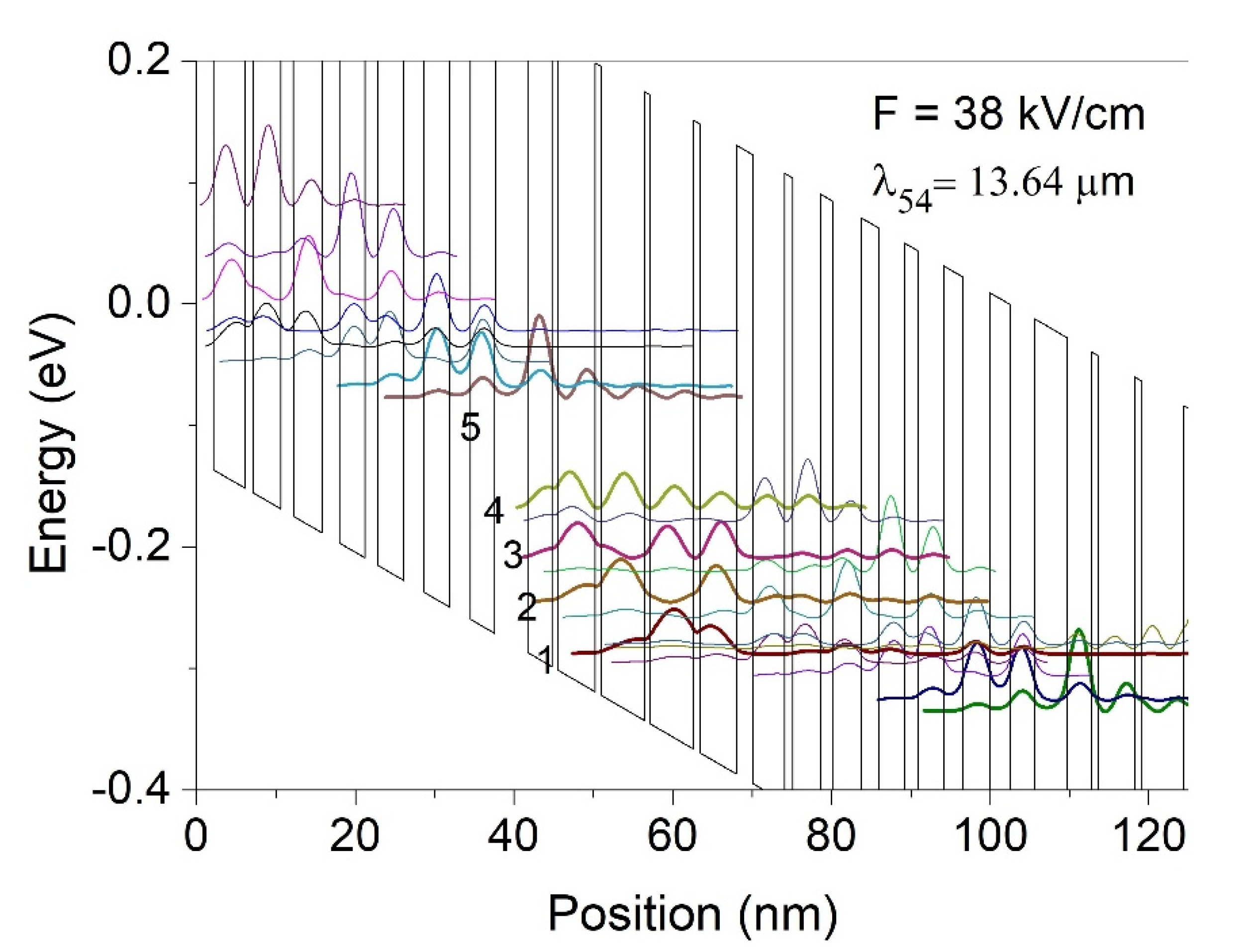
Figure 2.
The calculated changes of transition energy (black dots) and emission wavelength (red stars) resulting from group III elements flux changes.
Figure 2.
The calculated changes of transition energy (black dots) and emission wavelength (red stars) resulting from group III elements flux changes.
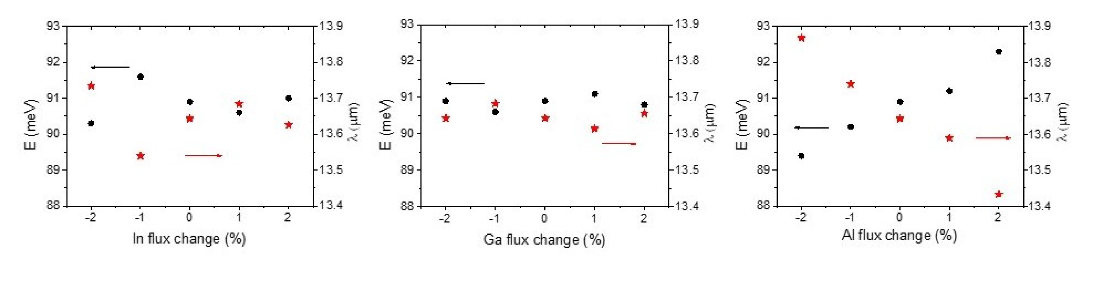
Figure 3.
The scheme of double superlattice structure. The thickness of InyAl1-yAs and InxGa1-xAs layers in SL1 was 2 nm while for SL2 were 2 nm and 4 nm for InyAl1-yAs and InxGa1-xAs, respectively. The period of SL1 was repeated 60 times and SL2 – 40 times. The nominal indium stoichiometric coefficient of InyAl1-yAs layers was 0.522 and InxGa1-xAs layers was 0.533 (lattice matched to InP).
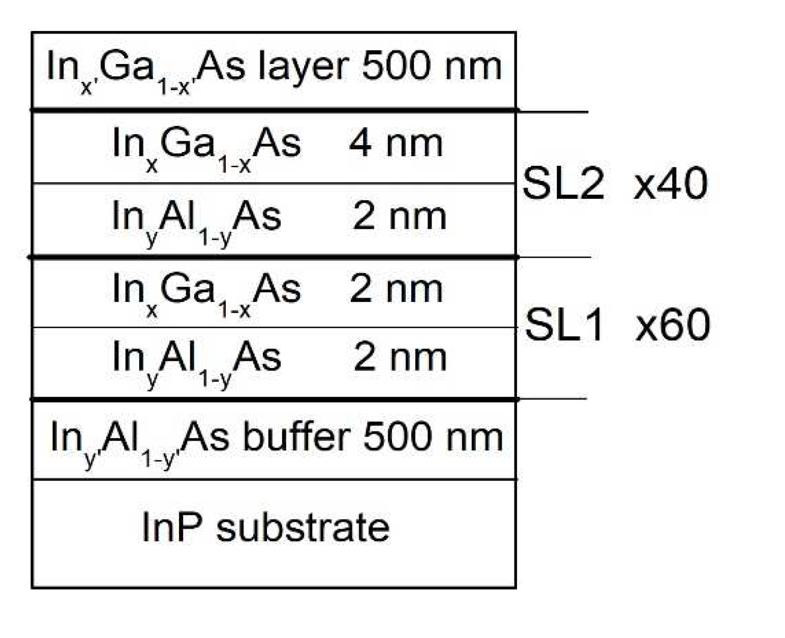
Figure 4.
The measured diffraction curves of double superlattice test structures.
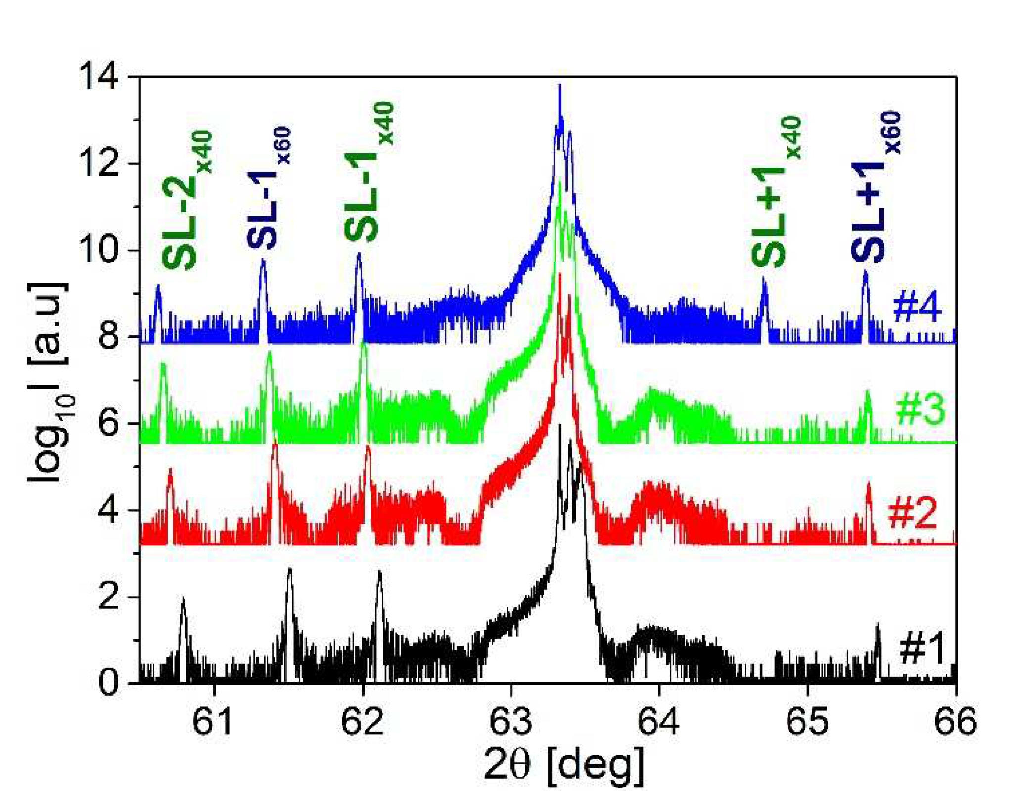
Figure 5.
The comparison of experimental 2θ/ω curve for SL #4 with simulated one (a). Detailed view of 2θ/ω curves (measured and simulated) with marked InP substrate, SL0x60/SLx40, Inx’Ga1-x’As layer and Iny’Al1-y’As buffer peaks (b).
Figure 5.
The comparison of experimental 2θ/ω curve for SL #4 with simulated one (a). Detailed view of 2θ/ω curves (measured and simulated) with marked InP substrate, SL0x60/SLx40, Inx’Ga1-x’As layer and Iny’Al1-y’As buffer peaks (b).
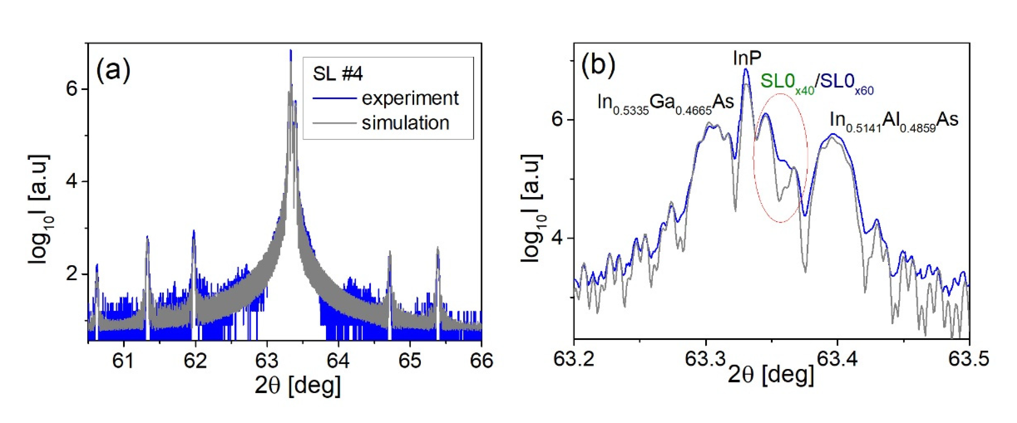
Figure 6.
Stoichiometric coefficient x of InxGa1-xAs thin layers (a) and stoichiometric coefficient y of InyAl1-yAs layers (b) obtained from self-consistent analysis of double superlattice test structures.
Figure 6.
Stoichiometric coefficient x of InxGa1-xAs thin layers (a) and stoichiometric coefficient y of InyAl1-yAs layers (b) obtained from self-consistent analysis of double superlattice test structures.
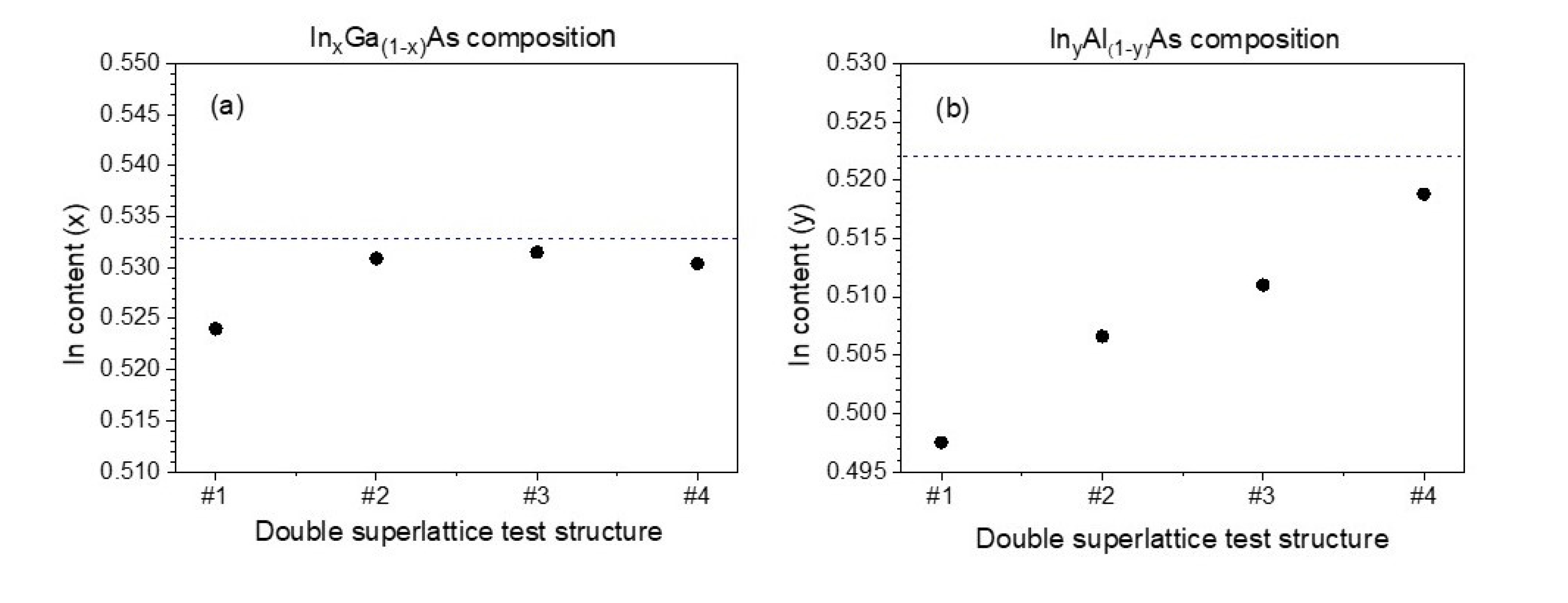
Figure 7.
QCL period values obtained from HRXRD measurements for six consecutive growth runs (a). The perpendicular lattice mismatch values of QCLs superlattice to the InP substrate obtained from SL0 peak position in HRXRD measurements for six consecutive growth runs (b).
Figure 7.
QCL period values obtained from HRXRD measurements for six consecutive growth runs (a). The perpendicular lattice mismatch values of QCLs superlattice to the InP substrate obtained from SL0 peak position in HRXRD measurements for six consecutive growth runs (b).
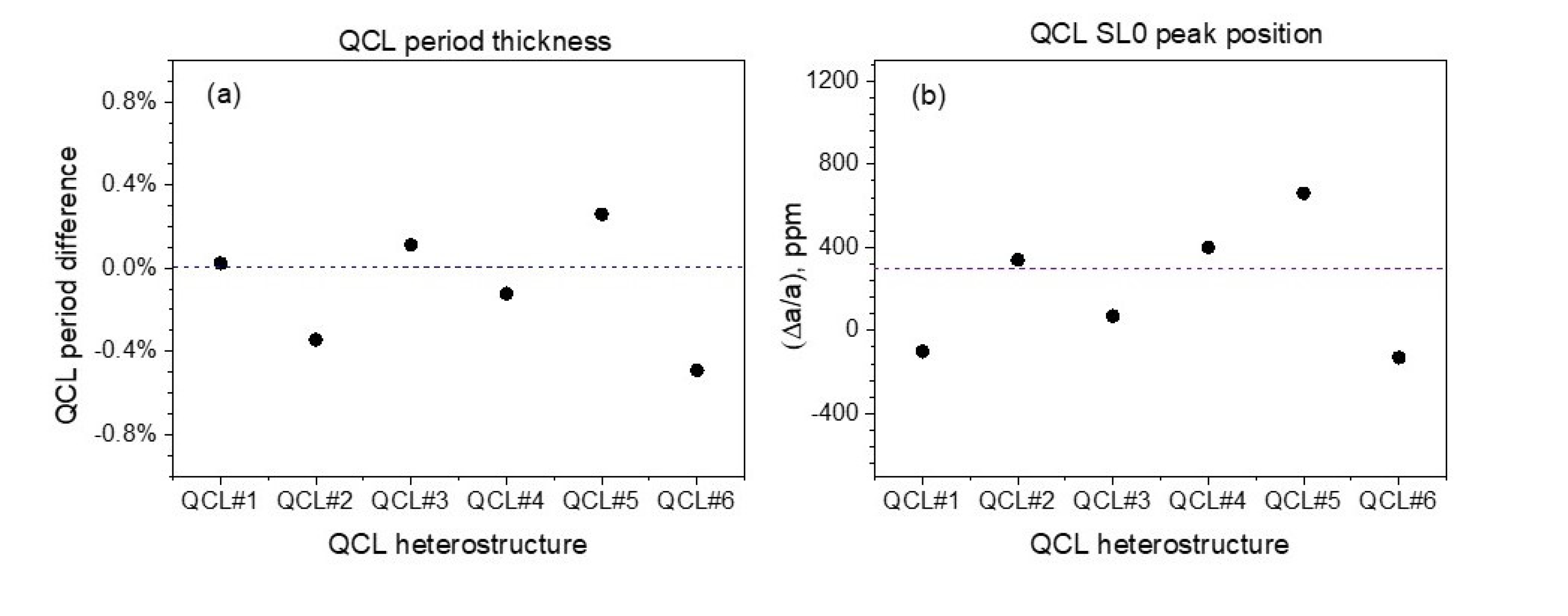
Figure 8.
Stoichiometric coefficient x of InxGa1-xAs layers in QCLs active region (a) and stoichiometric coefficient y of InyAl1-yAs layers in QCLs active region (b) obtained from simulation of measured diffraction curves for six consecutive growth runs.
Figure 8.
Stoichiometric coefficient x of InxGa1-xAs layers in QCLs active region (a) and stoichiometric coefficient y of InyAl1-yAs layers in QCLs active region (b) obtained from simulation of measured diffraction curves for six consecutive growth runs.

Figure 9.
The experimental 2θ/ω curve of #QCL4 QCL structure: full curve (a) and detailed view (b). The reciprocal lattice space points measured around InP for symmetrical 004 (c) and asymmetrical -2-24 reflections (d).
Figure 9.
The experimental 2θ/ω curve of #QCL4 QCL structure: full curve (a) and detailed view (b). The reciprocal lattice space points measured around InP for symmetrical 004 (c) and asymmetrical -2-24 reflections (d).

Figure 10.
The emission spectra of the lasers in the temperature range from 10 °C to 40 °C. The inset shows light-current and voltage-current (LIV) characteristics. The lasers were pulse driven by 200 ns pulses with 5 kHz repetition.
Figure 10.
The emission spectra of the lasers in the temperature range from 10 °C to 40 °C. The inset shows light-current and voltage-current (LIV) characteristics. The lasers were pulse driven by 200 ns pulses with 5 kHz repetition.
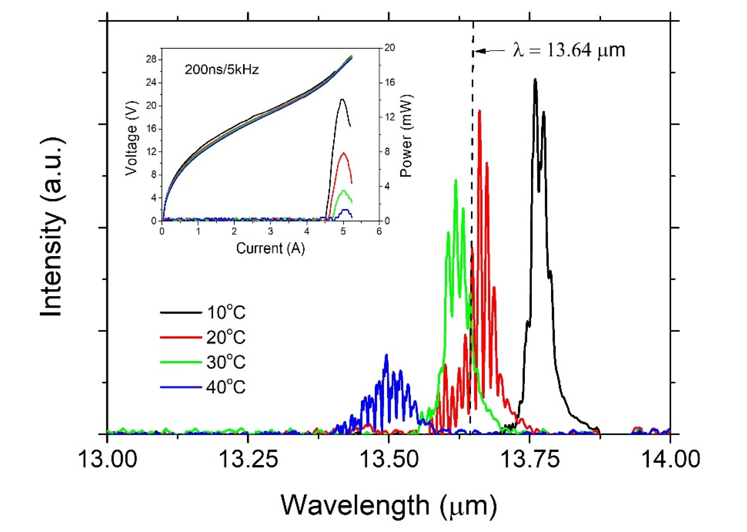
Table 1.
The values of composition of barriers and wells resulting from group III elements flux changes. The numbers refer to In content in the individual layers. The exact values of In content in lattice matched InAlAs and InGaAs are 0.522 and 0.533, respectively.
Table 1.
The values of composition of barriers and wells resulting from group III elements flux changes. The numbers refer to In content in the individual layers. The exact values of In content in lattice matched InAlAs and InGaAs are 0.522 and 0.533, respectively.
| Layer | In content | |||||
|---|---|---|---|---|---|---|
| -2% | -1% | Exact | +1% | +2% | ||
| In flux change | InAlAs | 0.517 | 0.520 | 0.522 | 0.525 | 0.527 |
| InGaAs | 0.528 | 0.530 | 0.533 | 0.535 | 0.538 | |
| Ga flux change | InAlAs | 0.522 | 0.522 | 0.522 | 0.522 | 0.522 |
| InGaAs | 0.538 | 0.535 | 0.533 | 0.530 | 0.528 | |
| Al flux change | InAlAs | 0.527 | 0.525 | 0.522 | 0.520 | 0.517 |
| InGaAs | 0.533 | 0.533 | 0.533 | 0.533 | 0.533 | |
Table 2.
The results of simulation of main parameters of the lasers grown at different values of group III elements fluxes. In all cases the lasers were under applied electric field of 38.0 kV/cm ( and are the upper laser level 5 and the lower laser level 4 lifetimes).
Table 2.
The results of simulation of main parameters of the lasers grown at different values of group III elements fluxes. In all cases the lasers were under applied electric field of 38.0 kV/cm ( and are the upper laser level 5 and the lower laser level 4 lifetimes).
| Exact value | In flux change | Ga flux change | Al flux change | ||||||||||
|---|---|---|---|---|---|---|---|---|---|---|---|---|---|
| -2% | -1% | 1% | 2% | -2% | -1% | 1% | 2% | -2% | -1% | 1% | 2% | ||
| ΔE54 (meV) | 90.9 | 90.3 | 91.6 | 90.6 | 91.0 | 90.9 | 90.6 | 91.1 | 90.8 | 89.4 | 90.2 | 91.2 | 92.3 |
| (μm) | 13.643 | 13.735 | 13.539 | 13.684 | 13.625 | 13.643 | 13.683 | 13.614 | 13.656 | 13.868 | 13.740 | 13.589 | 13.433 |
| z54 (nm) | 3.63 | 3.42 | 3.47 | 3.74 | 3.80 | 3.48 | 3.55 | 3.70 | 3.76 | 3.59 | 3.59 | 3.65 | 3.64 |
| (ps) | 3.1 | 3.7 | 3.3 | 2.9 | 2.8 | 3.5 | 3.3 | 3.0 | 2.9 | 3.4 | 3.3 | 3.1 | 2.9 |
| (ps) | 1.26 | 1.34 | 1.32 | 1.23 | 1.20 | 1.33 | 1.29 | 1.25 | 1.21 | 1.31 | 1.29 | 1.25 | 1.24 |
| (ps) | 0.35 | 0.36 | 0.36 | 0.35 | 0.34 | 0.35 | 0.35 | 0.35 | 0.34 | 0.35 | 0.35 | 0.35 | 0.34 |
| FoM | 1481 | 1419 | 1420 | 1512 | 1525 | 1442 | 1451 | 1508 | 1510 | 1505 | 1492 | 1470 | 1455 |
Table 3.
The structural parameters of double superlattice test structures obtained from self-consistent analysis; data received directly from measured 2θ/ω curve – in bold. The two last columns list parameters for Inx’Ga1-x’As layer and Iny’Al1-y’As buffer obtained from analysis of diffraction curves.
| SL1×60 / SL2x40 | Inx’Ga1-x’As top layer |
Iny’Al1-y’As buffer | ||||||
|---|---|---|---|---|---|---|---|---|
| SL | x InxGa1-xAs |
d, nm InxGa1-xAs |
y InyAl1-yAs |
d, nm InyAl1-yAs |
D, nm | (Δa/a), ppm | x’/(Δa/a), ppm | y’/(Δa/a), ppm |
| #1 | 0.5240 | 2.47/4.94 | 0.4975 | 2.77 | 5.24/7.71 | -2100/-1800 | 0.5242/-900 | 0.5135/-1000 |
| #2 | 0.5309 | 2.50/5.00 | 0.5066 | 2.69 | 5.19/7.69 | -960/-680 | 0.5311/0 | 0.5151/-880 |
| #3 | 0.5315 | 2.46/4.92 | 0.5110 | 2.69 | 5.15/7.61 | -660/-450 | 0.5328/230 | 0.5123/-1200 |
| #4 | 0.5304 | 2.46/4.92 | 0.5188 | 2.65 | 5.11/7.57 | -220/-170 | 0.5335/350 | 0.5141/-940 |
Disclaimer/Publisher’s Note: The statements, opinions and data contained in all publications are solely those of the individual author(s) and contributor(s) and not of MDPI and/or the editor(s). MDPI and/or the editor(s) disclaim responsibility for any injury to people or property resulting from any ideas, methods, instructions or products referred to in the content. |
© 2023 by the authors. Licensee MDPI, Basel, Switzerland. This article is an open access article distributed under the terms and conditions of the Creative Commons Attribution (CC BY) license (http://creativecommons.org/licenses/by/4.0/).
Copyright: This open access article is published under a Creative Commons CC BY 4.0 license, which permit the free download, distribution, and reuse, provided that the author and preprint are cited in any reuse.


