Submitted:
24 July 2023
Posted:
24 July 2023
You are already at the latest version
Abstract
The development of good conductivity p-type β-Ga2O3 is critical to realize its devices and applications. The nitrogen-doped p-type β-Ga2O3 films with enhanced conductivity characteristics were prepared through the thermal oxidation of GaN in the N2O atmosphere. Further measurements were performed on the oxidized films at 1000, 1050, and 1100 °C to have insight into the underlying mechanism of the thermally activated transformation process. The room temperature photoluminescence (PL) spectra demonstrated a moderate ultraviolet emission peak at 246 nm, confirming the generation of gallium oxide with a band gap of ~5.0 eV. The normalized X-ray diffraction (XRD), the high-resolution transmission electron microscopy (HRTEM), and the selected area electron diffraction (SAED) patterns were used to confirm the characteristic of polycrystalline and anisotropic growth. Then, the effects of the oxidation temperature on the amount of incorporated nitrogen were analyzed using secondary ion mass spectrometry (SIMS). Moreover, the ionization energy of the acceptor of films oxidized at 1000, 1050, and 1100 °C was calculated and analyzed using the temperature-dependent Hall test results. The results showed that nitrogen doping was the main contributor to p-type electrical properties. The activation energy of the polycrystalline β-Ga2O3 prepared through thermal oxidation of GaN in the N2O atmosphere was estimated to be 147.175 kJ·mol-1 using the Arrhenius plot, which was considerably lower than that of both dry and wet oxidations of GaN in O2 ambient, thus confirming the efficiency of thermal oxidation of GaN in N2O.
Keywords:
gallium oxide
; thermal oxidation
; p-type conductivity
; polycrystalline crystal
1. Introduction
Monoclinic β-Ga2O3, as the ultra-wide bandgap transparent semiconducting oxide, has attracted significant research focus [1,2,3,4]. Although having the notable thermal conductivity disadvantage, β-Ga2O3 currently has been used in the high power electronics, the kV-class Schottky barrier diodes [5,6,7], the e- and d-mode MOSFETs [8,9,10] and MESFETs [11], the solar-blind UV photodetectors [12,13], the light emitting diodes [14], sensing systems [15,16], solar cells [17], photocatalysts [18] and phosphors [19].
At present, bulk single crystals of β-Ga2O3 are grown through the Czochralski [20] and the EFG methods [21] with a reasonable size and structural quality. Moreover, high structural quality homo-epitaxial layers were obtained using MOVPE [22] and MBE [23]. The grown β-Ga2O3 can be either electrical insulators or n-type semiconductors. It can be grown via intentional doping with the electron concentration tunable between 1016 and 1019 cm−3, Hall electron conductivity ranging from 10-12 to 102 S∙cm-1, and Hall electron mobility up to 170 cm2∙V−1∙s−1 [24,25,26]. However, the development of the improved p-type conductivity in β-Ga2O3 has not been effectively achieved. Therefore, the demand for further study on appropriate acceptor doping is necessary [27,28,29].
Nitrogen is one of the promising acceptor species for Ga2O3. For substituting O, nitrogen is the closest to O in terms of atomic size but has one less valence electron than O. Studies have been conducted and reported on the generation of the p-type nitrogen-doped β-Ga2O3 films [30,31] and the nanowires [32,33] through thermal oxidation GaN in O2 atmosphere at 1000 to 1100 °C. Moreover, our previous study demonstrated the successful growth of p-type nitrogen-doped β-Ga2O3 films using the low bond energy N2O gas for the thermal oxidation of GaN [34]. Because N2O can be easily decomposed into O atoms and ‘N=N’, it can effectively complete the oxidation substitution. Therefore, the p-type β-Ga2O3 films produced in the N2O atmosphere have higher Hall hole concentration and higher conductivity than thermal oxidation of GaN with O2 at the same temperature range.
The technology of nitrogen-doping for β-Ga2O3 needs to be explored in detail. Given the same experimental results presented in the previous study [34], this study focused on the analysis of the characteristics at 1000, 1050, and 1100 °C, in which the grown β-Ga2O3 achieved the Hall hole concentrations above 2.55 × 1016 cm−3. This study aimed to: (1) further corroborate the prepared films are polycrystalline β-Ga2O3 using PL, normalized XRD, HRTEM, and SAED; (2) explore the variations in nitrogen-doping concentration using secondary ion mass spectrometry (SIMS) within the oxidation temperature range; (3) determine the primary acceptor by analyzing the valence band spectrum and calculating the ionization energy of the acceptor; (4) explore the advantage of oxidation efficiency in N2O atmosphere by calculating the activation energy. The activation energy in this study was 147.175 kJ·mol-1. To our knowledge, the activation energies of dry and wet oxidations of GaN using oxygen were 300 kJ·mol-1 [35] and 210 kJ·mol-1 [36], respectively.
2. Experimental Procedure
The un-doped (native n-type with an electron concentration of 1.02 × 1017 cm-3) (0001) GaN wafers with 5.8-5.9 µm thickness were heated in a horizontal quartz tube furnace to 1000, 1050, and 1100 °C under N2O gas at a flow rate of 200 cc∙min-1 for 60 min. More details of the experimental parameters can be found in [34].
A fluorescence spectrometer (PI-PLE-2355/2558+PIXIS-256E, Princeton Instruments) was used to measure the room temperature PL spectra using two different light sources at different wavelength ranges. The light source was obtained at a wavelength ranging from 242 to 300 nm by grating spectrophotometry. In addition, at a wavelength range of 325-700 nm, the light source was the 325 nm He-Cd laser.
Then the phase structure of the samples was identified with the normalized XRD (Malvern Panalytical EMPYREAN SERIES 3) using Cu Kα (λ = 1.54 Å) X-ray source at a 2-theta range of 10 to 80º using a sampling pitch and preset time of 0.02º and 0.24 s, respectively.
Transmission electron microscopy (TEM) on Talos F200X S/TEM at 200 kV was used to determine the oxide thickness and analyze the cross-sectional microstructure. The cross-sectional specimens were prepared using focused ion beam (FIB) milling (Helos-5UX), and the phases and lattice structure were further investigated using HRTEM and SAED.
The depth profiles of Ga, O, and N in the films oxide at 1000, 1050, and 1100 °C were qualitatively analyzed using SIMS (TOF.SIMS5-100). During SIMS measurements, the secondary ions were detected using 5 keV Cs + bombardment at an incidence angle of 60º to distribute ions. X-ray photoelectron spectroscopy (XPS, ThermoFisher ESCALAB Xi+) was used to investigate the valence band characteristic of β-Ga2O3. Before the XPS measurement, the applied voltage of 15 kV accelerated the Ar ion beam at a sputtering rate of 0.10 nm∙s−1 for 100 s to etch 10 nm depth into the samples. The XPS analysis revealed the valence band characteristic on the β-Ga2O3 layer. Moreover, the XPS analysis further confirmed the variation in the N-doping ratio and Ga/O ratio with oxidation temperature.
Indium electrodes were sputtered on the films, followed by rapid thermal annealing (RTA) at 600 °C for 60 s to form a good ohmic contact. Given the electrical property test results using the temperature-dependent (70 to 540K) Rmagnetic-field-dependent Van der Pauw Hall effect measurements (PPMS DynaCool-9) under a vacuum test environment, the acceptor ionization energies were calculated from the linear regression formula of ln(p) versus 1000/T.
3. Results and discussion
The room temperature PL spectrum measurements were conducted to determine the nature of the grown films as a function of the oxidation temperature. Figure 1a depicts the PL spectra (at a wavelength ranging from 242 to 300 nm) of the samples obtained through thermal oxidation at 1000, 1050, and 1100 °C. Although the light source by grating spectrophotometry was weak, a fairly distinct emission peak around 246 nm (~5.0 eV) was observed in all grown films. The observed emission peak was attributed to the band-to-band luminescence of gallium oxide, confirming that Ga2O3 was successfully produced through the thermal oxidation of GaN. Moreover, the peak intensity around 246 nm increased 2.6 times, and the full width at half-maximum significantly decreased with increasing oxidation temperature, indicating that the oxide layer became thicker. Figure 1b and its inset show the PL spectra of the oxidation films and the un-doped commercial GaN substrate within the wavelength range of 325-700 nm for comparison using the 325 nm He-Cd laser as a light source. The emission peaks at 355 nm (~3.491 eV) and 366 nm (~3.387 eV) belonged to GaN [37]. As the temperature of thermal oxidation increased, these two emission peaks of GaN decreased. Besides, comparing with the PL from the GaN substrate, the yellow emission at 565 nm (~2.194 eV) in the oxide films was ascribed to the Ga vacancies during high-temperature growth [38,39].
The XRD patterns of the grown films as a function of the oxidation temperature confirmed the formation of the β-Ga2O3 phase with a preferred orientation along the {01} directions. The XRD results were compared with the standard powder diffraction files of PDF# 43-1013 for β-Ga2O3 and PDF# 50-0792 for GaN. As shown in Figure 2, to compensate for the impact of large differences in oxidation depth on the corresponding intensity of XRD, each diffraction peak was normalized by the highest diffraction peak from the most preferred orientation at the same oxidation temperature. When the oxidation temperature was between 1000 and 1050 °C, the most preferred orientation was (01) located at 18.7°. Then, at 1100 °C, the most preferred orientation was (02) located at 38.2°. In addition to the {01} family of planes at 18.7°, 38.2°, and 59.1°, there were relatively strong diffraction peaks belonging to {400}, (002), (12), and (020) phases of β-Ga2O3, indicating that the β-Ga2O3 thin film obtained through high-temperature thermal oxidation was polycrystalline.
The SAED pattern of a detailed characterization of the grown β-Ga2O3 film is shown in Figure 3a–c. The discrete bright spots belonged to the (01), (02), (002), (111), (020), and (400) crystal planes of β-Ga2O3, further demonstrating the polycrystalline nature of the β-Ga2O3 thin film. Additionally, for the sample thermally oxidized at 1000, 1050, and 1100 °C, the enlarged HRTEM images (Figure 3d–f) of the region around the β-Ga2O3/GaN interface displayed a clear boundary between the β-Ga2O3 film and the GaN substrate without transition zone. Moreover, the crystal plane orientations of the β-Ga2O3 thin film in HRTEM images ulteriorly confirmed the polycrystalline nature of the β-Ga2O3 thin film.
For the samples thermally oxidized at 900, 950, 1000, 1050, and 1100 °C, the natural logarithm plot of the oxide layer thickness (ln (Thickness)) as the function of oxidation temperature (1000/T) is cumulatively plotted in Figure 4. Based on the oxidation thickness, the activation energy required for thermal oxidation (0001) of monocrystalline GaN to form polycrystalline β-Ga2O3 in the N2O atmosphere was analyzed. The Arrhenius equation described the temperature dependence of chemical reactions better. Therefore, the activation energy was calculated using the idealized Arrhenius law behavior shown in equation (1) according to our experiments of thermal oxidation of GaN in the N2O atmosphere at 900 to 1100°C:
where k is the Boltzmann constant; is the thickness of β-Ga2O3 at 900 °C [34], taking as the initial thickness of the oxidation process; T is oxidation temperature in Kelvin. The activation energy calculated from equation (1) was approximately 147.175 kJ·mol-1. In the previous studies, the reported results of activation energies of dry and wet thermal oxidations of GaN in O2 ambient were 300 [35] and 210 kJ·mol-1 [36], respectively. This result quantitatively shows that the O atom in the low bond energy under the N2O atmosphere can easily get free from the covalent bond at the same temperature. As a result, the oxidation rate was relatively fast, and the activation energy required was relatively low.
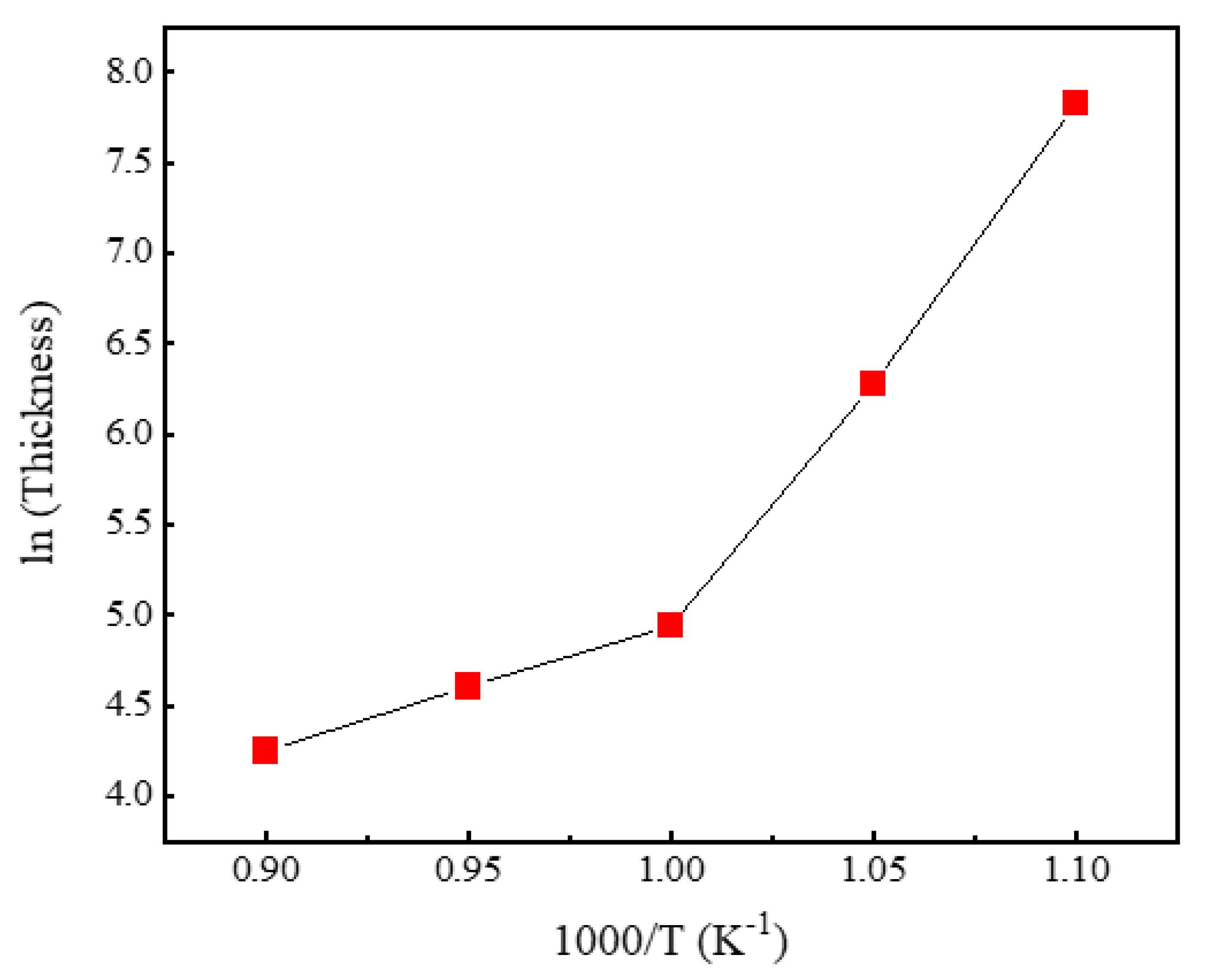
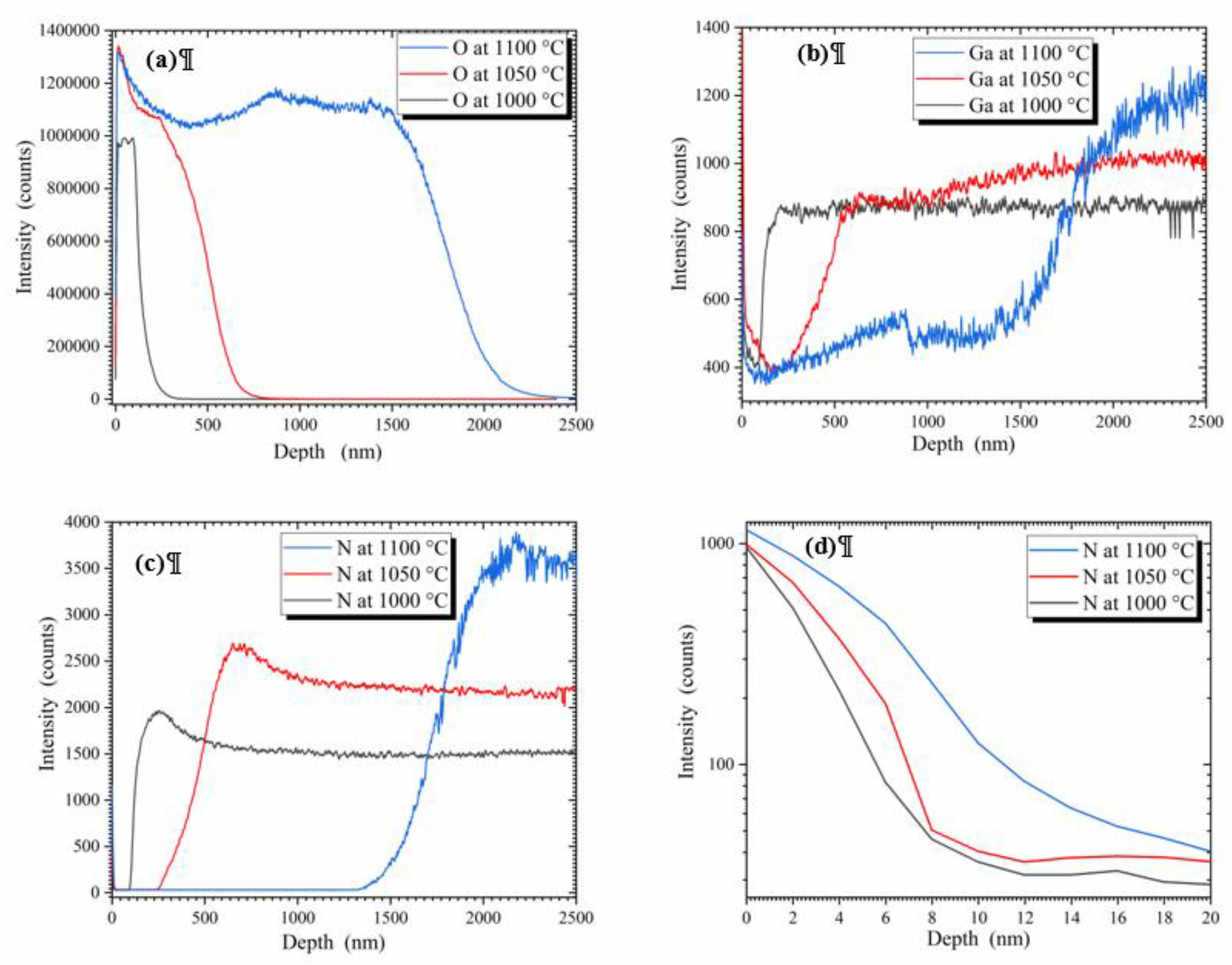
Figure 4.
The natural logarithm plot of the oxide layer thickness (ln (Thickness)) as the function of oxidation temperature (1000/T) for the thermally oxidized samples at 900, 950, 1000, 1050, and 1100 °C.
Figure 4.
The natural logarithm plot of the oxide layer thickness (ln (Thickness)) as the function of oxidation temperature (1000/T) for the thermally oxidized samples at 900, 950, 1000, 1050, and 1100 °C.
Figure 5.
SIMS characterizations of the depth profiles of (a) O, (b) Ga, (c) N from 0 to 2.5 μm depth for the thermally oxidized samples at 1000, 1050, and 1100 °C. (d) The enlarged view of the N with a depth of 0-20 nm.
Figure 5.
SIMS characterizations of the depth profiles of (a) O, (b) Ga, (c) N from 0 to 2.5 μm depth for the thermally oxidized samples at 1000, 1050, and 1100 °C. (d) The enlarged view of the N with a depth of 0-20 nm.
In Figure 6a–c, for the samples thermally oxidized at 1000, 1050 and 1100 °C, the O, Ga, and N elemental’s vertical distributions from SIMS were exhibited. The depth of the analysis includes the topmost surface layer to the depth of 2.5 µm. Figure 6a shows the O ion response intensities of the SIMS test as a function of depth. The thickness of β-Ga2O3 films at 1000, 1050, and 1100 °C to be 145 nm, 530 nm, and 2.5 μm, respectively. These results were consistent with the longitudinal distribution depth of O in SIMS results (Figure 6a). As shown in Figure 6a, within the β-Ga2O3 layer, the O content gradually reduced in the downward direction approaching the β-Ga2O3/GaN interface. At all three oxidation temperatures, the higher the oxidation temperature, the higher the reduction of O content when approaching the interface. The main reason for the insufficient O was that the N atoms in the underlying GaN were separated by thermal oxidation and gradually moved upward; thus, in the β-Ga2O3 layer, N replaced O to form the N-doped β-Ga2O3. Moreover, the N was more abundant close to the interface; as a result, it substituted more O, thus decreasing O content. In addition, at a higher temperature, the O in the β-Ga2O3 is more likely to be released from the covalent bond and escape from the polycrystalline β-Ga2O3 layer. Therefore, O vacancies existed in the grown β-Ga2O3 layer. Figure 6b shows the Ga ion response intensities of the SIMS test as a function of depth. In the grown β-Ga2O3 layer, the stoichiometric ratio of Ga:O is 2:3. In the GaN substrate, the stoichiometric ratio of Ga:N 1:1. The test mode of SIMS in this study was based on the relative content ratio of elements. As shown in Figure 6a,b, the content of Ga was relatively low within the range of the depth of the corresponding β-Ga2O3 layer. The content of Ga was relatively high in the depth range of the corresponding GaN layer. Moreover, the depth position of the change in Ga content was consistent with the observed oxidation thickness of FIB, indicating that the β-Ga2O3 layer was indeed successfully oxidized. As shown in Figure 6b, the Ga content close to the top of the β-Ga2O3 was lower than that of the stoichiometric of β-Ga2O3, indicating that Ga vacancies were formed by the high-temperature oxidation close to the β-Ga2O3 surface. Figure 6c shows the N ion response intensities as a function of depth obtained from the SIMS test. As shown in Figure 6c, the position where the N content became stable corresponded to the interface position between the β-Ga2O3 and the GaN layer. Moreover, the portion of N within the β-Ga2O3 region decomposed from GaN and transmitted to the β-Ga2O3 layer above it, increasing the relative N concentration. In the β-Ga2O3 layer, the lower the position close to the GaN layer, the higher the N-doping concentration. However, further away from the GaN layer, the N-doping decreased. To interpret the effect of N atoms separated from N2O on N-doping in the β-Ga2O3 layer, Figure 6d shows an enlarged view of the N from 0 to 20 nm depth of the thermally oxidized samples at 1000, 1050, and 1100 °C. Although the decomposed N from N2O also participated in the N-doping, the doping depth was relatively shallow, and the doping concentration was low at a depth of 20 nm. The N-O bond in N2O was a single bond with low bond energy; thus, the O atom was easily separated at high temperatures. In contrast, the two N atoms in N2O were double-bonded. Consequently, high bond energy was required to break the two double-bonded N atoms, meaning that the proportion of N separated at high temperatures was relatively low. As shown in Figure 6c,d, the decomposed N from GaN was the main source of N-doping in grown β-Ga2O3.
To further support the relative proportions of elements observed during the SIMS tests, the elemental ratios of N and the Ga/O observed using XPS are presented in Table 1. According to the stoichiometric ratio (Ga/O is ~0.6667), the polycrystalline β-Ga2O3 grown through thermal oxidation always exhibited an O-deficient state in the Ga/O ratio (Table 1). In the process of oxidation, although O vacancies were formed, the key reason for O deficiency was that N replaced O rather than O vacancies. Moreover, as the oxidation temperature increased, the proportion of G decreased slightly, implied that the Ga vacancies increased slightly with the increase of oxidation temperature. In addition, as oxidation temperature increased, the proportion of N in the β-Ga2O3 layer increased. This result is consistent with that of N response intensities in SIMS. It also confirms that the p-type conductivity of the films improves with the increase in oxidation temperature.
XPS was used to investigate the valence band characteristic of the thermally oxidized samples at 1000, 1050, and 1100 °C (Figure 7a–e). Both theoretical studies [40,41] and experimental results [42,43] have demonstrated that the density of states for the valence band is predominated by the O 2p character. And the Ga 3d peak was used as the calibration peak. As the oxidation temperature went up, the valence band edge of O 2p shifted further to the right, and the moved valence band (Figure 7a,b) accordingly, indicating a lower Fermi level and more p-type characteristic. Figure 7c–e show the enlarged tail parts of the valence band for the thermally oxidized samples at 1000, 1050, and 1100 °C, respectively. The ordinates of Figure 7c–e, counts per second (counts/s), are normalized to the maximum value ranging from 0 to 5 eV. The variation trend of the slope at the turning point of the tail confirmed the presence of states in the lower part of the bandgap. As the oxidation temperature increased, the shallow acceptor levels introduced by N-doping moved closer toward the valence band, indicating a larger p-type carrier density, thus improving p-type conductivity.
The temperature-dependent Hall measurements were conducted (from 70 to 540 K) on the samples oxidized at 1000, 1050, and 1100 °C under a vacuum environment. The positive Hall coefficients confirmed that the N-doped β-Ga2O3 films were p-type. The variations in Hall hole concentration, Hall hole mobility, and Hall resistivity of samples as the function of the test temperature are highlighted in Figure 7a–c, respectively. In addition, the natural logarithm plot of Hall hole concentration (ln (p)) as the function of (1000/T) is shown in Figure 7d. With the increase in test temperature, the changes in Hall hole concentration, Hall mobility, and Hall resistivity of the three samples were consistent and showed a reasonable trend. As the test temperature increased from 70 to 540 K, Hall carrier concentration increased, whereas Hall mobility and Hall resistivity decreased. Under the same test temperature, the higher the oxidation temperature, the more N-doping in the β-Ga2O layer formed through oxidation, thus contributing higher Hall hole concentration, better Hall mobility, and smaller Hall resistivity. At a test temperature of 300 K, the Hall hole concentrations of the three samples were 2.55 × 1016 cm-3(@1000 °C oxidation temperature), 6.31 × 1016 cm-3 (@1050 °C oxidation temperature), and 1.63693 × 1017 cm-3(@1100 °C oxidation temperature). PL and SIMS results showed that Ga and O vacancies existed in β-Ga2O films obtained through high-temperature oxidation. VGa and the pairs of VGa-VO might act as potential acceptors [44,45,46]. However, based on the near-band-edge structure of β-Ga2O3 nanostrips depicted in Figure 7 of [47], the transition energy of the acceptor level VGa ~0.494 eV (E0 - ED1) [47]. At 300 K, this order of magnitude ionization energy can only contribute near 1015 order of magnitude for hole concentration. Therefore, the Hall hole concentration ranging from 2.55 × 10¹⁶ to 1.63693 × 1017 cm-3 was mainly contributed by N-doping in β-Ga2O3. β-Ga2O3 thin films with fairly good Hall hole concentration were obtained through oxidation technology. The carrier concentration increased in proportion to oxidation temperature. However, although the mobility also increased with the rise of oxidation temperature, the increase of mobility was not that much. (Figure 2b). This phenomenon was because when the oxidation temperature increased from 1000 to 1100 °C, more loose hollows were generated inside the cross-section of the β-Ga2O3 film. As a result, the defects and dangling bonds were introduced near the hollows, which in turn hindered the improvement of mobility. Therefore, no significant increase was observed in overall mobility. At a test temperature of 300 K, the Hall hole mobilities were 2.2 cm2∙V−1∙s−1 (@1000 °C oxidation temperature), 3.3 cm2∙V−1∙s−1 (@1050 °C oxidation temperature), and 5 cm2∙V−1∙s−1 (@1100 °C oxidation temperature). Similarly, the Hall resistivity slightly decreased. At a test temperature of 300 K, the Hall hole motilities are 74 Ω∙cm (@1000 °C oxidation temperature), 45 Ω∙cm (@1050 °C oxidation temperature), and 7.7 Ω∙cm (@1100 °C oxidation temperature). Figure 7d displays the natural logarithm plot of Hall hole concentration (ln (p)) as the function of (1000/T). Based on the linear regression formula of ln(p) versus 1000/T, the acceptor ionization energies of oxidized samples at 1000, 1050, and 1100°C were similar, which were ~0.092 ± 0.005 eV. The smaller acceptor ionization energy implies the easier hole activation of the N-doping instead of Ga vacancies for the β-Ga2O3 film. This phenomenon further demonstrates that N-doping mainly contributes to p-type electrical conductivity.
4. Conclusion
Nitrogen-doping acceptor in β-Ga2O3 with Hall hole concentration ranging from 2.55 × 1016 cm−3 to 1.63693 × 1017 cm-3 was realized through thermal oxidation of GaN in N2O atmosphere at temperatures of 1000 to 1100 °C. The structural analysis using PL, normalized XRD, and FIB-TEM confirmed that grown β-Ga2O3 films were polycrystalline. The calculation of activation energy based on oxidation thickness confirmed that the process of thermal oxidation and nitrogen-doping in the N2O atmosphere was more efficient than that in an oxygen atmosphere. Finally, the analysis of the valence band energy spectrum and Hall electrical property revealed that the p-type conductivity of the polycrystalline β-Ga2O3 was mainly realized by substituting O in β-Ga2O3 with N.
Author Contributions
Sufen Wei designed the experimental and test schemes, organized the data, and wrote the paper; Yi Liu performed the experiments and analyzed the data and measurements; Qianqian Shi and Tinglin He analyzed the data and measurements; Feng Shi helped with analyzing the basic principles and writing the paper; and Ming-Kwei Lee put forward the idea of experiment, guided the analysis of the experimental results, and helped with editing the English.
Funding
This work was supported by the Foreign Cooperation Project of Fujian Provincial Department of Science and Technology (Grant No. 2020I0022).
Institutional Review Board Statement
Not applicable.
Informed Consent Statement
Not applicable.
Data Availability Statement
Not applicable.
Conflicts of Interest
The authors declare no conflict of interest.
References
- Pearton, S.J.; Yang, J.; Cary, P.H., IV; Ren, F.; Kim, J.; Tadjer, M.J.; Mastro, M.A. A review of Ga2O3 materials, processing, and devices. Appl. Phys. Rev. 2018, 5, 011301. [Google Scholar] [CrossRef]
- Higashiwaki, M.; Sasaki, K.; Murakami, H.; Kumagai, Y.; Koukitu, A.; Kuramata, A.; Masui, T.; Yamakoshi, S. Recent progress in Ga2O3power devices. Semicond. Sci. Technol. 2016, 31, 034001. [Google Scholar] [CrossRef]
- Galazka, Z. β-Ga2O3 for wide-bandgap electronics and optoelectronics. Semicond. Sci. Technol. 2018, 33, 113001. [Google Scholar] [CrossRef]
- Mastro, M.A.; Kuramata, A.; Calkins, J.; Kim, J.; Ren, F.; Pearton, S.J. Perspective—Opportunities and Future Directions for Ga2O3. ECS J. Solid State Sci. Technol. 2017, 6, P356–P359. [Google Scholar] [CrossRef]
- Konishi, K.; Goto, K.; Murakami, H.; Kumagai, Y.; Kuramata, A.; Yamakoshi, S.; Higashiwaki, M. 1-kV vertical Ga2O3 field-plated Schottky barrier diodes. Appl. Phys. Lett. 2017, 110. [Google Scholar] [CrossRef]
- Sasaki, K.; Higashiwaki, M.; Kuramata, A.; Masui, T.; Yamakoshi, S. $\hbox{Ga}_{2} \hbox{O}_{3}$ Schottky Barrier Diodes Fabricated by Using Single-Crystal $\beta$– $\hbox{Ga}_{2} \hbox{O}_{3}$ (010) Substrates. IEEE Electron Device Lett. 2013, 34, 493–495. [Google Scholar] [CrossRef]
- Higashiwaki, M.; Konishi, K.; Sasaki, K.; Goto, K.; Nomura, K.; Thieu, Q.T.; Togashi, R.; Murakami, H.; Kumagai, Y.; Monemar, B.; et al. Temperature-dependent capacitance–voltage and current–voltage characteristics of Pt/Ga2O3 (001) Schottky barrier diodes fabricated on n––Ga2O3 drift layers grown by halide vapor phase epitaxy. Appl. Phys. Lett. 2016, 108, 133503. [Google Scholar] [CrossRef]
- Hu, Z.; Nomoto, K.; Li, W.; Tanen, N.; Sasaki, K.; Kuramata, A.; Nakamura, T.; Jena, D.; Xing, H.G. Enhancement-Mode Ga2O3 Vertical Transistors With Breakdown Voltage >1 kV. IEEE Electron Device Lett. 2018, 39, 869–872. [Google Scholar] [CrossRef]
- Chabak, K.D.; Moser, N.; Green, A.J.; Walker, D.E.; Tetlak, S.E.; Heller, E.; Crespo, A.; Fitch, R.; McCandless, J.P.; Leedy, K.; et al. Enhancement-mode Ga2O3 wrap-gate fin field-effect transistors on native (100) β-Ga2O3 substrate with high breakdown voltage. Appl. Phys. Lett. 2016, 109, 213501. [Google Scholar] [CrossRef]
- Higashiwaki, M.; Sasaki, K.; Kamimura, T.; Wong, M.H.; Krishnamurthy, D.; Kuramata, A.; Masui, T.; Yamakoshi, S. Depletion-mode Ga2O3 metal-oxide-semiconductor field-effect transistors on β-Ga2O3 (010) substrates and temperature dependence of their device characteristics. Appl. Phys. Lett. 2013, 103, 123511. [Google Scholar] [CrossRef]
- Dang, G.T.; Kawaharamura, T.; Furuta, M.; Allen, M.W. Mist-CVD Grown Sn-Doped $\alpha $ -Ga2O3 MESFETs. IEEE Trans. Electron Devices 2015, 62, 3640–3644. [Google Scholar] [CrossRef]
- Kaur, D.; Kumar, M. A Strategic Review on Gallium Oxide Based Deep-Ultraviolet Photodetectors: Recent Progress and Future Prospects. Adv. Opt. Mater. 2021, 9, 2002160. [Google Scholar] [CrossRef]
- Oh, S.; Jung, Y.; Mastro, M.A.; Hite, J.K.; Eddy, C.R.; Kim, J. Development of solar-blind photodetectors based on Si-implanted β-Ga_2O_3. Opt. Express 2015, 23, 28300–5. [Google Scholar] [CrossRef] [PubMed]
- Xu, J.; Zheng, W.; Huang, F. Gallium oxide solar-blind ultraviolet photodetectors: a review. J. Mater. Chem. C 2019, 7, 8753–8770. [Google Scholar] [CrossRef]
- Chiang, J.-L.; Shang, Y.-G.; Yadlapalli, B.K.; Yu, F.-P.; Wuu, D.-S. Ga2O3 nanorod-based extended-gate field-effect transistors for pH sensing. Mater. Sci. Eng. B 2021, 276, 115542. [Google Scholar] [CrossRef]
- Das, M.; Chakraborty, T.; Lin, C.Y.; Lin, R.-M.; Kao, C.H. Screen-printed Ga2O3 thin film derived from liquid metal employed in highly sensitive pH and non-enzymatic glucose recognition. Mater. Chem. Phys. 2022, 278. [Google Scholar] [CrossRef]
- Minami, T.; Nishi, Y.; Miyata, T. High-Efficiency Cu2O-Based Heterojunction Solar Cells Fabricated Using a Ga2O3Thin Film as N-Type Layer. Appl. Phys. Express 2013, 6, 044101. [Google Scholar] [CrossRef]
- Wang, X.; Xu, Q.; Li, M.; Shen, S.; Wang, X.; Wang, Y.; Feng, Z.; Shi, J.; Han, H.; Li, C. Photocatalytic Overall Water Splitting Promoted by an α-β phase Junction on Ga2O3. Angew. Chem. 2012, 124, 13266–13269. [Google Scholar] [CrossRef]
- Galazka, Z.; Uecker, R.; Klimm, D.; Irmscher, K.; Naumann, M.; Pietsch, M.; Kwasniewski, A.; Bertram, R.; Ganschow, S.; Bickermann, M. Scaling-Up of Bulk β-Ga2O3Single Crystals by the Czochralski Method. ECS J. Solid State Sci. Technol. 2016, 6, Q3007–Q3011. [Google Scholar] [CrossRef]
- Kuramata, A.; Koshi, K.; Watanabe, S.; Yamaoka, Y.; Masui, T.; Yamakoshi, S. High-quality β-Ga2O3 single crystals grown by edge-defined film-fed growth. Jpn. J. Appl. Phys. 2016, 55, 1202A2. [Google Scholar] [CrossRef]
- Chou, T.-S.; Bin Anooz, S.; Grüneberg, R.; Irmscher, K.; Dropka, N.; Rehm, J.; Tran, T.T.V.; Miller, W.; Seyidov, P.; Albrecht, M.; et al. Toward Precise n-Type Doping Control in MOVPE-Grown β-Ga2O3 Thin Films by Deep-Learning Approach. Crystals 2021, 12, 8. [Google Scholar] [CrossRef]
- Sasaki, K.; Kuramata, A.; Masui, T.; Víllora, E.G.; Shimamura, K.; Yamakoshi, S. Device-Quality $\beta$-Ga$_{2}$O$_{3}$ Epitaxial Films Fabricated by Ozone Molecular Beam Epitaxy. Appl. Phys. Express 2012, 5. [Google Scholar] [CrossRef]
- Neal, A.T.; Mou, S.; Rafique, S.; Zhao, H.; Ahmadi, E.; Speck, J.S.; Stevens, K.T.; Blevins, J.D.; Thomson, D.B.; Moser, N.; et al. Donors and deep acceptors in β-Ga2O3. Appl. Phys. Lett. 2018, 113, 062101. [Google Scholar] [CrossRef]
- Ahmadi, E.; Koksaldi, O.S.; Kaun, S.W.; Oshima, Y.; Short, D.B.; Mishra, U.K.; Speck, J.S. Ge doping of β-Ga2O3 films grown by plasma-assisted molecular beam epitaxy. Appl. Phys. Express 2017, 10. [Google Scholar] [CrossRef]
- Sasaki, K.; Higashiwaki, M.; Kuramata, A.; Masui, T.; Yamakoshi, S. Si-Ion Implantation Doping in β-Ga2O3and Its Application to Fabrication of Low-Resistance Ohmic Contacts. Appl. Phys. Express 2013, 6, 086502. [Google Scholar] [CrossRef]
- Zhang, J.; Shi, J.; Qi, D.-C.; Chen, L.; Zhang, K.H.L. Recent progress on the electronic structure, defect, and doping properties of Ga2O3. APL Mater. 2020, 8, 020906. [Google Scholar] [CrossRef]
- Wong, M.H.; Lin, C.-H.; Kuramata, A.; Yamakoshi, S.; Murakami, H.; Kumagai, Y.; Higashiwaki, M. Acceptor doping of β-Ga2O3 by Mg and N ion implantations. Appl. Phys. Lett. 2018, 113, 102103. [Google Scholar] [CrossRef]
- Lyons, J.L. A survey of acceptor dopants forβ-Ga2O3. Semicond. Sci. Technol. 2018, 33, 05LT02. [Google Scholar] [CrossRef]
- Wu, Z.; Jiang, Z.; Ma, C.; Ruan, W.; Chen, Y.; Zhang, H.; Zhang, G.; Fang, Z.; Kang, J.; Zhang, T.-Y. Energy-driven multi-step structural phase transition mechanism to achieve high-quality p-type nitrogen-doped β-Ga2O3 films. Mater. Today Phys. 2021, 17, 100356. [Google Scholar] [CrossRef]
- Jiang, Z.; Wu, Z.; Ma, C.; Deng, J.; Zhang, H.; Xu, Y.; Ye, J.; Fang, Z.; Zhang, G.; Kang, J.; et al. P-type β-Ga2O3 metal-semiconductor-metal solar-blind photodetectors with extremely high responsivity and gain-bandwidth product. Mater. Today Phys. 2020, 14, 100226. [Google Scholar] [CrossRef]
- Wu, Z.; Jiang, Z.; Song, P.; Tian, P.; Hu, L.; Liu, R.; Fang, Z.; Kang, J.; Zhang, T. Nanowire-Seeded Growth of Single-Crystalline (010) β-Ga 2 O 3 Nanosheets with High Field-Effect Electron Mobility and On/Off Current Ratio. Small 2019, 15, e1900580. [Google Scholar] [CrossRef] [PubMed]
- Song, P.; Wu, Z.; Shen, X.; Kang, J.; Fang, Z.; Zhang, T.-Y. Self-consistent growth of single-crystalline (2̄01)β-Ga2O3nanowires using a flexible GaN seed nanocrystal. CrystEngComm 2016, 19, 625–631. [Google Scholar] [CrossRef]
- Liu, Y.; Wei, S.; Shan, C.; Zhao, M.; Lien, S.-Y.; Lee, M.-K. Compositions and properties of high-conductivity nitrogen-doped p-type β-Ga2O3 films prepared by the thermal oxidation of GaN in N2O ambient. J. Mater. Res. Technol. 2022, 21, 3113–3128. [Google Scholar] [CrossRef]
- Wolter, S.D.; Mohney, S.E.; Venugopalan, H.; Wickenden, A.E.; Koleske, D.D. Kinetic Study of the Oxidation of Gallium Nitride in Dry Air. J. Electrochem. Soc. 1998, 145, 629–632. [Google Scholar] [CrossRef]
- Readinger, E.D.; Wolter, S.D.; Waltemyer, D.L.; Delucca, J.M.; Mohney, S.E.; Prenitzer, B.I.; Giannuzzi, L.A.; Molnar, R.J. Wet thermal oxidation of GaN. J. Electron. Mater. 1999, 28, 257–260. [Google Scholar] [CrossRef]
- Lee, I.-H.; Lee, C.-R.; Shin, D.C.; Nam, O.; Park, Y. Correlations between photoluminescence and Hall mobility in GaN/sapphire grown by metalorganic chemical vapor deposition. J. Cryst. Growth 2004, 260, 304–308. [Google Scholar] [CrossRef]
- Yang J, Zhao D, Jiang D, Chen P, Liu Z, Zhu J, et al. Different variation behaviors of resistivity for high-temperature-grown and low-temperature-grown p-GaN films. Chin. Phys. B. 2016;25,027102-1-4. [CrossRef]
- Lu, W.; Terazawa, M.; Han, D.-P.; Sone, N.; Goto, N.; Iida, K.; Murakami, H.; Iwaya, M.; Tekeuchi, T.; Kamiyama, S.; et al. Structural and optical impacts of AlGaN undershells on coaxial GaInN/GaN multiple-quantum-shells nanowires. Nanophotonics 2019, 9, 101–111. [Google Scholar] [CrossRef]
- Cocchi, C.; Zschiesche, H.; Nabok, D.; Mogilatenko, A.; Albrecht, M.; Galazka, Z.; Kirmse, H.; Draxl, C.; Koch, C.T. Atomic signatures of local environment from core-level spectroscopy inβ−Ga2O3. Phys. Rev. B 2016, 94, 075147. [Google Scholar] [CrossRef]
- He, H.; Orlando, R.; Blanco, M.A.; Pandey, R.; Amzallag, E.; Baraille, I.; Rérat, M. First-principles study of the structural, electronic, and optical properties ofGa2O3in its monoclinic and hexagonal phases. Phys. Rev. B 2006, 74, 195123. [Google Scholar] [CrossRef]
- Navarro-Quezada, A.; Galazka, Z.; Alamé, S.; Skuridina, D.; Vogt, P.; Esser, N. Surface properties of annealed semiconducting β-Ga2O3 (1 0 0) single crystals for epitaxy. Appl. Surf. Sci. 2015, 349, 368–373. [Google Scholar] [CrossRef]
- Navarro-Quezada, A.; Alamé, S.; Esser, N.; Furthmüller, J.; Bechstedt, F.; Galazka, Z.; Skuridina, D.; Vogt, P. Near valence-band electronic properties of semiconductingβ−Ga2O3(100) single crystals. Phys. Rev. B 2015, 92. [Google Scholar] [CrossRef]
- Korhonen, E.; Tuomisto, F.; Gogova, D.; Wagner, G.; Baldini, M.; Galazka, Z.; Schewski, R.; Albrecht, M. Electrical compensation by Ga vacancies in Ga2O3 thin films. Appl. Phys. Lett. 2015, 106. [Google Scholar] [CrossRef]
- Chikoidze, E.; Sartel, C.; Mohamed, H.; Madaci, I.; Tchelidze, T.; Modreanu, M.; Vales-Castro, P.; Rubio, C.; Arnold, C.; Sallet, V.; et al. Enhancing the intrinsic p-type conductivity of the ultra-wide bandgap Ga2O3 semiconductor. J. Mater. Chem. C 2019, 7, 10231–10239. [Google Scholar] [CrossRef]
- Chikoidze, E.; Fellous, A.; Perez-Tomas, A.; Sauthier, G.; Tchelidze, T.; Ton-That, C.; Huynh, T.T.; Phillips, M.; Russell, S.; Jennings, M.; et al. P-type β-gallium oxide: A new perspective for power and optoelectronic devices. Mater. Today Phys. 2017, 3, 118–126. [Google Scholar] [CrossRef]
- Ho, C.-H.; Tseng, C.-Y.; Tien, L.-C. Thermoreflectance characterization of β-Ga_2O_3 thin-film nanostrips. Opt. Express 2010, 18, 16360–16369. [Google Scholar] [CrossRef]
Figure 1.
(a) PL emission spectra of the thermally oxidized samples at 1000, 1050, and 1100 ℃ within the wavelength range of 242-300 nm at room temperature. The emission was excited using grating spectrophotometry. (b) PL emission spectra of the thermally oxidized samples at 1000, 1050, and 1100°C within the wavelength range of 325–700 nm at room temperature. The inserted image is the PL spectrum of the undoped GaN substrate. The emission was excited using a 325-nm He-Cd laser.
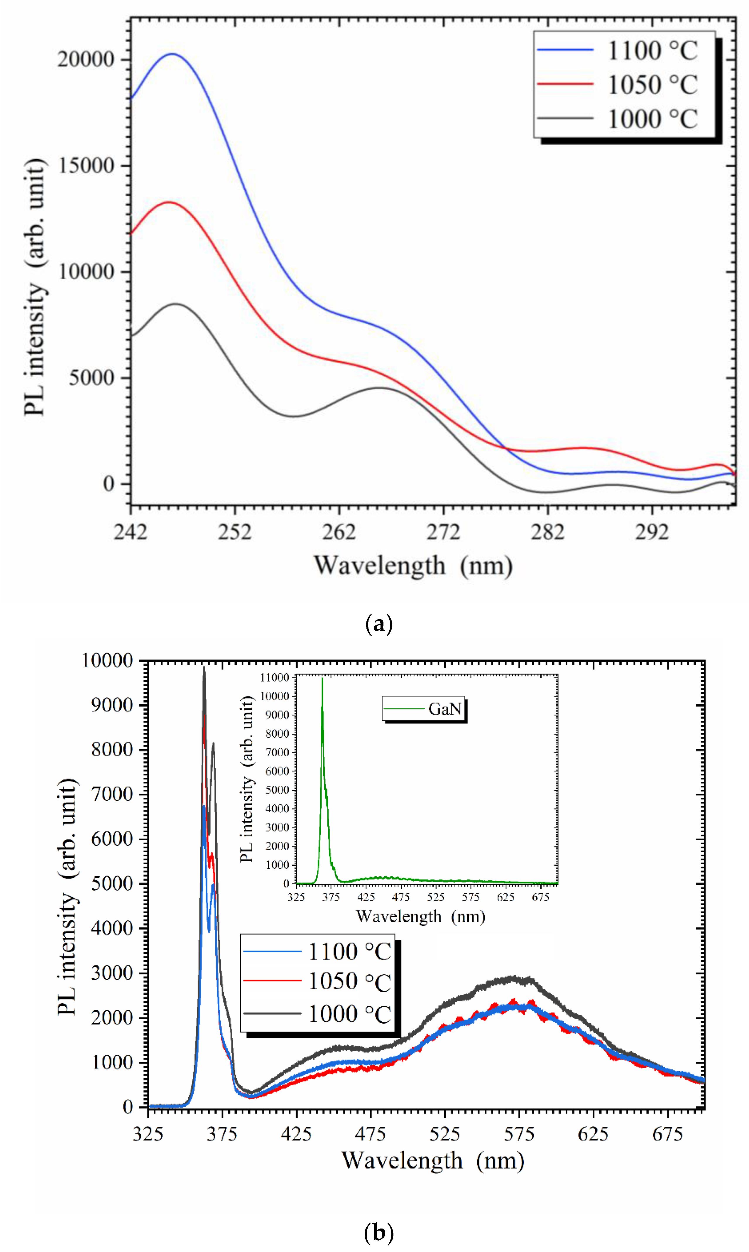
Figure 2.
Normalized XRD patterns of thermally oxidized samples at 1000, 1050, and 1100 °C compared with ICDD file PDF# 43-1013 for β-Ga2O3 and PDF# 50-0792 for GaN.
Figure 2.
Normalized XRD patterns of thermally oxidized samples at 1000, 1050, and 1100 °C compared with ICDD file PDF# 43-1013 for β-Ga2O3 and PDF# 50-0792 for GaN.
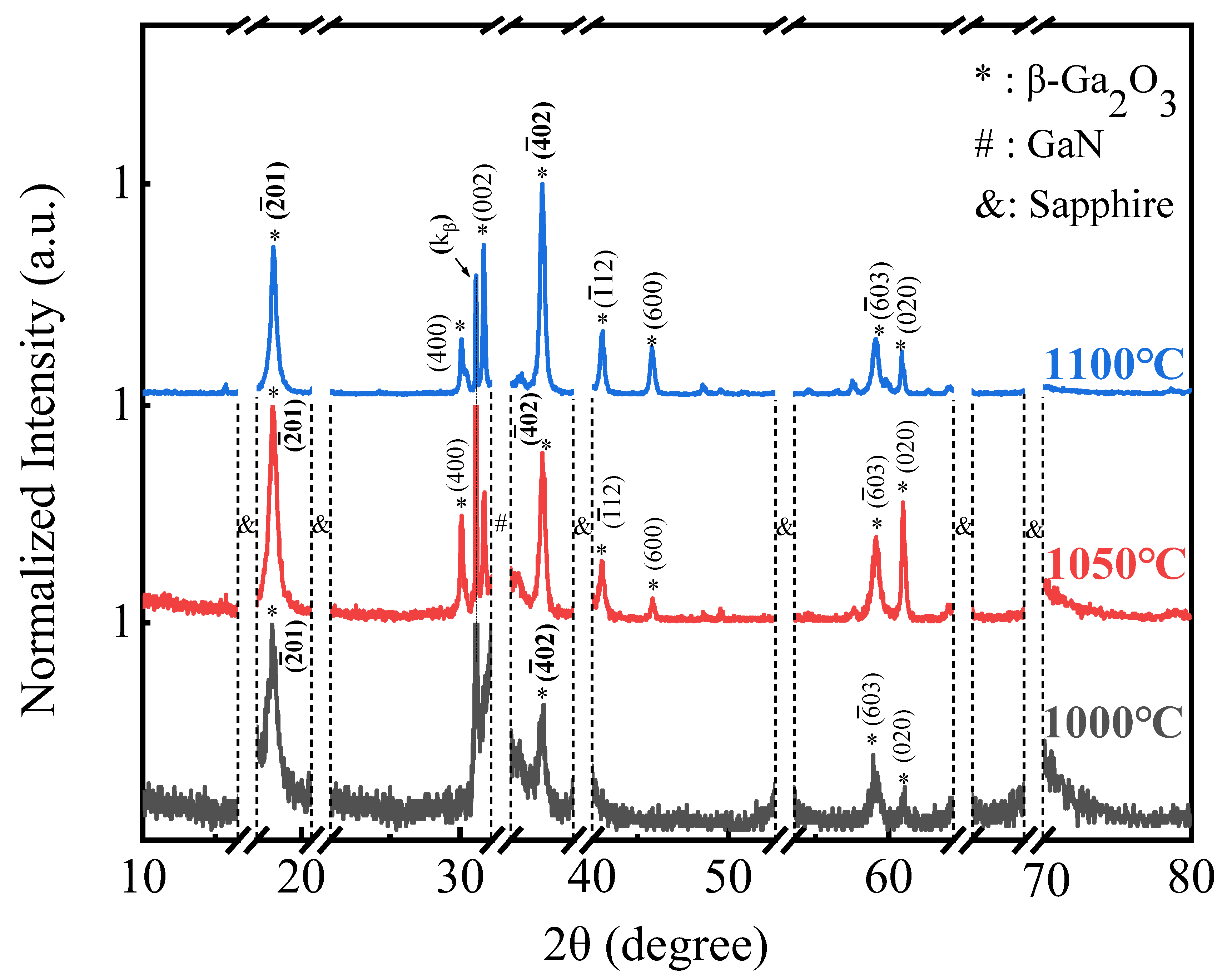
Figure 3.
The SEAD patterns of the β-Ga2O3 layer grown at (a) 1000 °C, (b) 1050 °C, and (c) 1100 °C, and the corresponding HRTEM images taken from the β-Ga2O3/GaN interface of the thermally oxidized samples (d) 1000 °C, (e) 1050 °C, and (f) 1100 °C.
Figure 3.
The SEAD patterns of the β-Ga2O3 layer grown at (a) 1000 °C, (b) 1050 °C, and (c) 1100 °C, and the corresponding HRTEM images taken from the β-Ga2O3/GaN interface of the thermally oxidized samples (d) 1000 °C, (e) 1050 °C, and (f) 1100 °C.
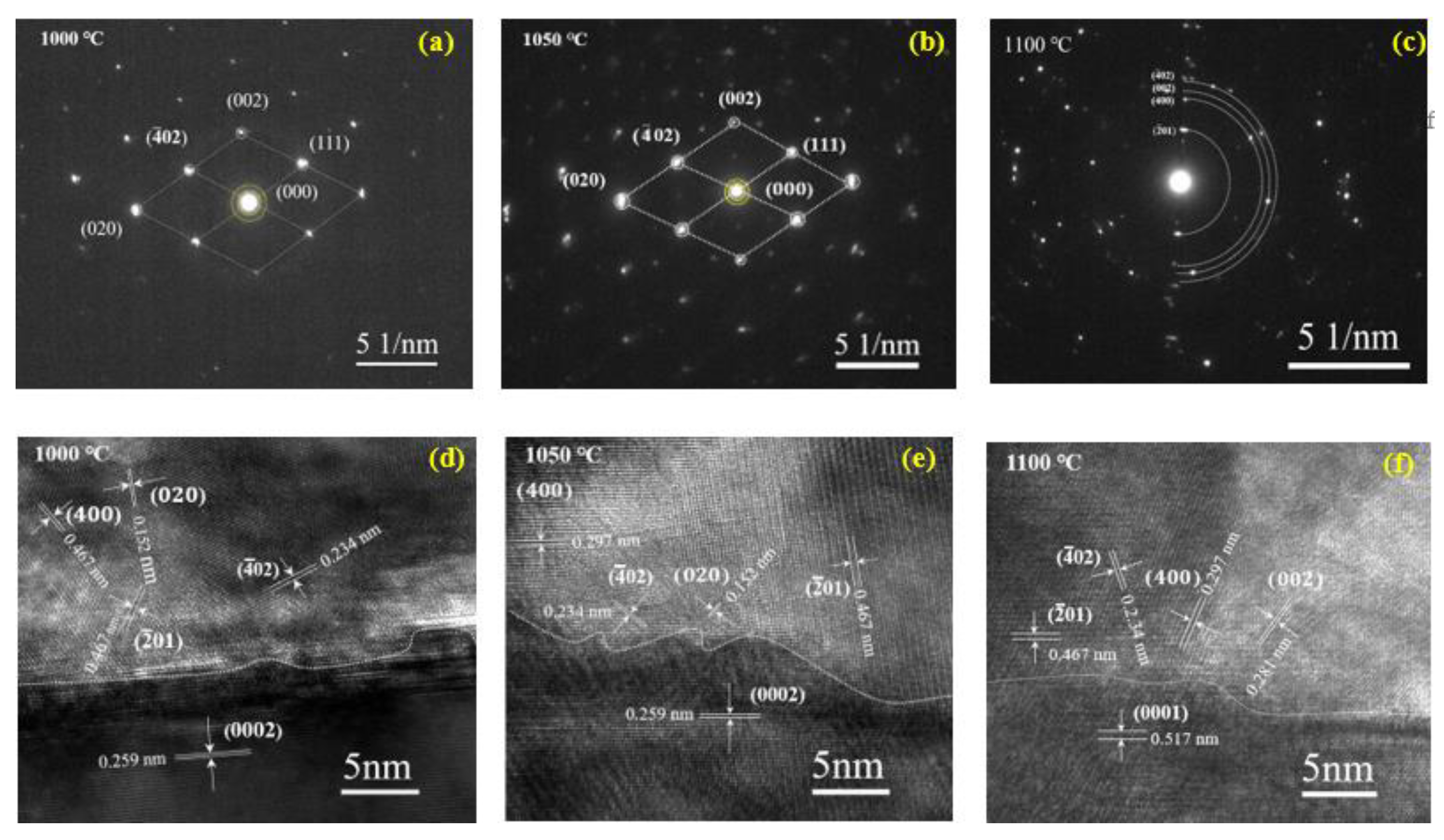
Figure 6.
(a) X-ray photoelectron spectroscopy of the β-Ga2O3 valence band for the thermally oxidized samples at 1000, 1050, and 1100 °C (calibrated with respect to Ga 3d). (b) A zoom of the valence band region for the O 2p characteristic peak. Further investigation of the tail states of the valence band for the thermally oxidized samples at (c) 1000 °C, (d) 1050 °C, and (e) 1100 °C.
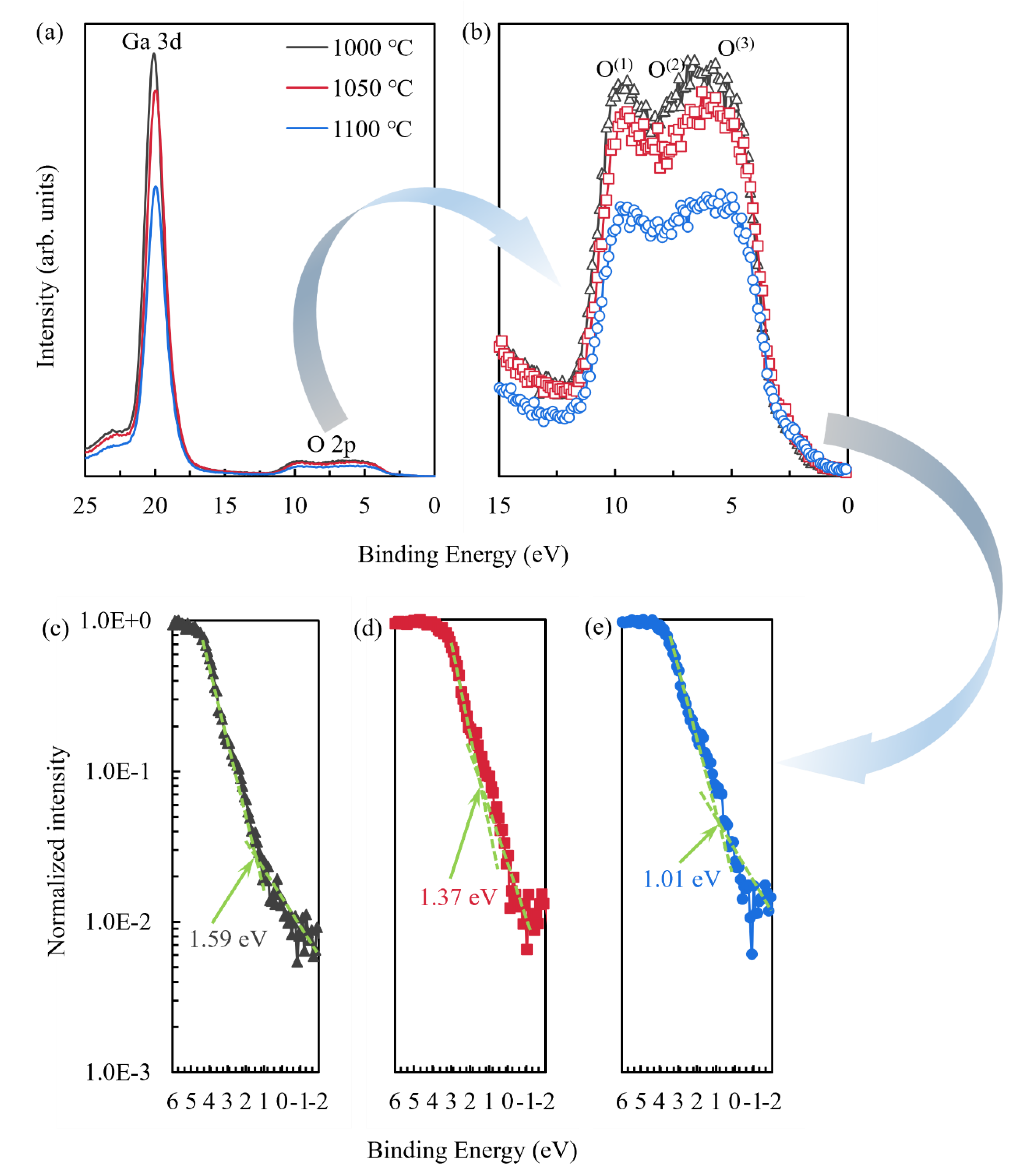
Figure 7.
For the thermally oxidized samples at 1000, 1050, and 1100 °C, the variations in (a) Hall hole concentration, (b) Hall hole mobility, and (c) Hall resistivity as a function of the test temperature. (d) The natural logarithm plot of Hall hole concentration (ln (p)) as the function of (1000/T).
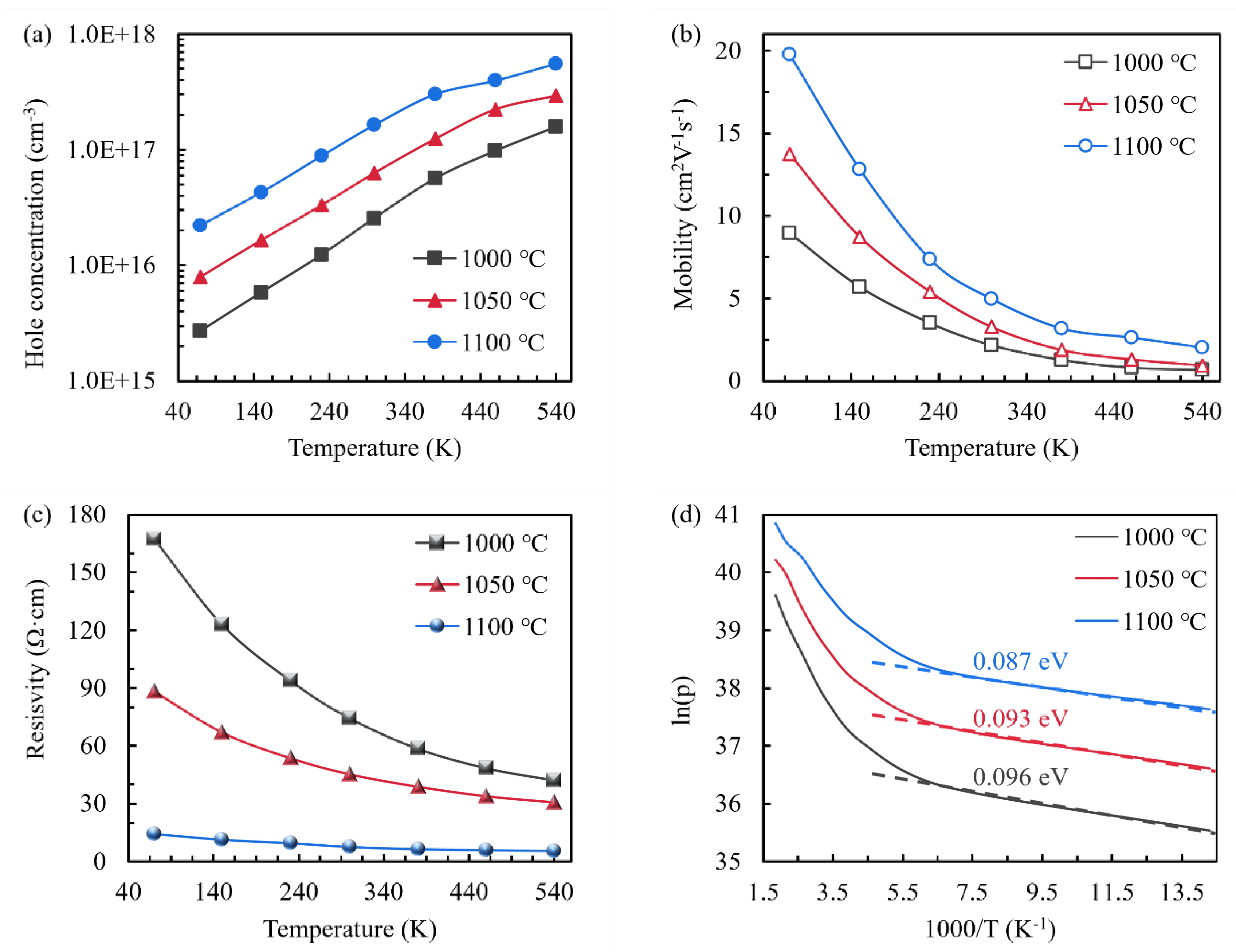

Table 1.
The elemental ratio of N and Ga/O ratio values from XPS.
| Oxidation temperature (°C) | 1000 | 1050 | 1100 |
|---|---|---|---|
| Ga/O ratio | 0.831 | 0.821 | 0.818 |
| N elemental ratio (%) | 0.0323 | 0.0369 | 0.0878 |
Disclaimer/Publisher’s Note: The statements, opinions and data contained in all publications are solely those of the individual author(s) and contributor(s) and not of MDPI and/or the editor(s). MDPI and/or the editor(s) disclaim responsibility for any injury to people or property resulting from any ideas, methods, instructions or products referred to in the content. |
© 2023 by the authors. Licensee MDPI, Basel, Switzerland. This article is an open access article distributed under the terms and conditions of the Creative Commons Attribution (CC BY) license (http://creativecommons.org/licenses/by/4.0/).
Copyright: This open access article is published under a Creative Commons CC BY 4.0 license, which permit the free download, distribution, and reuse, provided that the author and preprint are cited in any reuse.


