Preprint
Article

A Low Latency, Low Jitter Retimer Circuit for PCIe 6.0

Altmetrics

Downloads

308

Views

105

Comments

0

A peer-reviewed article of this preprint also exists.

Submitted:

07 June 2023

Posted:

08 June 2023

You are already at the latest version

Alerts
Abstract
As the PCIe 6.0 specification places higher requirements on signal integrity and transmission la-tency, it becomes especially important to improve signal transmission performance at the physical layer of the transceiver interface. Retimer circuit as a key component of high-speed serial interface, its delay and jitter size directly affect the overall performance of PCIe. For the conventional Retimer circuit with large latency and low jitter performance, this paper proposes a low latency and low jitter Retimer circuit based on CDR+PLL architecture for PCIe 6.0, using a jitter canceling filter circuit to eliminate the frequency difference between the retiming clock and data, reduce the retiming clock jitter, and improve the quality of Retimer output data; The data is sampled using the retiming clock and then output, avoiding the problem of large penetration latency of con-ventional Retimer circuits. The circuit is designed using CMOS 28nm process. Simulation results show that when 112Gbps PAM4 data is input to the Retimer circuit, the Retimer penetration la-tency is 27.3 ps, which is 83.5% lower than the conventional Retimer structure; the output data jitter is 741 fs, a 31.4% reduction compared to the conventional Retimer structure.
Keywords: 
Subject: Engineering  -   Electrical and Electronic Engineering

1. Introduction

Since its official release, PCIe (PCI-Express) has evolved rapidly and has become an indispensable technology for high-performance computer (HPC) communications [1], Ethernet, industrial control, etc. The release of the PCIe 6.0 specification has dramatically increased computing speeds for applications such as HPC, cloud computing, and data center solid state drives (SSD), but with that comes the negative impact of the channel on clock signals and transmitted data. Severe signal attenuation and interference limit the overall performance of PCIe 6.0, especially on the receiving end where signal integrity and transmission latency are greatly affected. As shown in Figure 1, Retimer, a technology for data synchronization and transmission, plays a key role in the physical layer of the PCIe 6.0 interface subsystem and is expected to be the primary solution in the PCIe 6.0 era with its better performance and more economical processing.
Since PCIe 3.0, the data rate has doubled with each new generation of the standard. PCIe 6.0 has increased the data transfer rate to 64GT/s, and the single channel bandwidth has reached 63.02Gbps. Retimer, as a PHY chip, needs to be compatible with various key technologies such as serialization and deserialization, clock generation and distribution, clock data recovery, data drive and equalization, etc. For the ultra-high speed input signal of 100Gbps or more, the synchronization signal still has large jitter and signal transmission also has large latency. In the circuit design, when there is a latency difference between the clock and data path, the correlation of the clock to data sampling is weakened [2], resulting in an increase in the correlation jitter between the clock and data path, which reduces the jitter tolerance. Therefore, many studies have minimized the delay matching between clock and data through clock sampling and forwarding techniques, which in turn achieve noise filtering and jitter cancellation. In [2], the receiver-side clock path uses a high-bandwidth filtered PLL to track data-related jitter and cut off high-frequency jitter, but this method does not guarantee that the PLL output clock and data path are at the same frequency; the literature [3] uses a Multiplying Delay Looked Loop (MDLL) to reset the oscillator jitter at the rate of the reference clock frequency, which does not require a high bandwidth loop to suppress oscillator jitter, reducing the complexity of the design, but this can subject the MDLL to large duty cycle distortion. A region-efficient phase filtering technique is proposed in [4] to filter jitter between cascaded repeaters, but the noise environment is not fundamentally eliminated and the jitter accumulated by subsequent cascaded circuits degrades the system performance and jitter tolerance. To reduce the output jitter, [5] uses a Retimer design with symmetric layout, reduces the differential coupling capacitance, adjusts the serial data and clock phase into the Retimer by a phase regulator with the help of an external control signal, and provides the clock drive for the Retimer, but this design cannot eliminate the phase difference between data and clock, and also increases the circuit penetration latency. In the literature [6], a retiming driver based on Clock And Data Recovery (CDR) + Vertical Cavity Surface Emitting Laser (VCSEL) architecture is designed for 50 Gbps PAM4 (Pulse-Amplitude - Modulation-4) signal; To address the challenges posed by signal characteristics, skinning effects, dielectric losses, and inter-symbol crosstalk, the Retimer of the repeater type was chosen as the signal conditioning technique in the literature [7]. The Retimer consists of a receiver and a driver that uses the clock recovered from the data stream by the CDR or a reference clock to achieve synchronous driving of the data. The literature [8] proposes a PAM4 transceiver architecture based on Analog to Digital Converter (ADC) + Digital Signal Processor (DSP), which makes the channel equalization capability greater than 40 dB for solving the encapsulation insertion loss caused in long distance transmission .In [9], an FPGA-based low-latency transfer scheme is used to achieve high-speed data transfer between the FPGA platform and the server. However, this scheme does not consider the data compression process which is more time consuming for transmission and the data transfer rate is still at a low level. A low latency forward error correction coding was proposed in [10],this technique has too much resource overhead in the coding layer.
In this paper, we propose a new Retimer solution to address the problem of latency and jitter in high-speed data transmission, in order to recover low-jitter data at the SerDes receiver and reduce the latency of data transmission in subsequent circuits.

2. Retimer Circuit Latency and Jitter Performance Analysis

Retimer contains the CDR circuit, which is the core component of SerDes PHY, and the Rx signal is reduced to a digital signal in Retimer, then reconverted to an analog signal and sent out through its Rx. The essence is to use PLL to recover data from clock jitter introduced by connector channel crosstalk, cable and board impedance distortion, and then send the signal out through the serial channel, which can reduce signal jitter and can better reduce physical loss. It shows that Retimer contains the CDR function can effectively filter the received signal jitter, but the complex high-speed Retimer will lead to poor quality recovery signal due to timing constraints, and it is easy to timeout and increase the line latency. As shown in Figure 2, the process of CDR recovery data sent out again goes through parallel-serial conversion, decoding and descrambling, and timing adjustment, which are time-consuming.
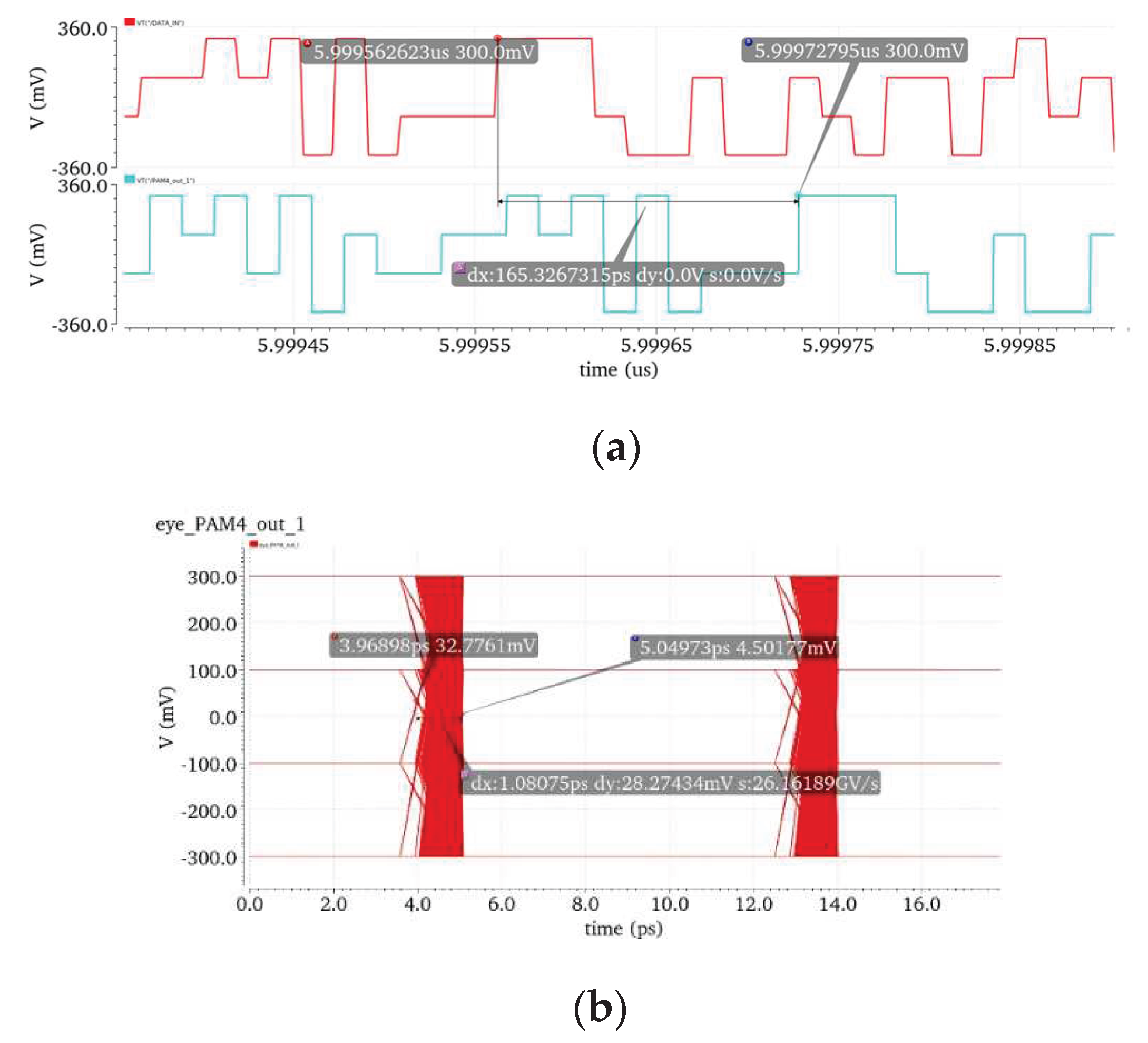
A 112Gbps PAM4 signal with a sinusoidal jitter amplitude of 0.1UI and a frequency of 1MHz is fed to the conventional Retimer circuit, and the latency and jitter measurements are shown in Figure 3. Figure 3a shows that the signal penetration latency in the circuit is 165.3ps from the input to the output, and Figure 3b shows that the jitter value of the transmitted data is 1.08 ps, with a jitter attenuation of -10.38 dB compared to the input signal. Although the latency characteristics and jitter characteristics of the circuit are good, they are still not enough for a high-speed signal of 112 Gbps.
From the above analysis, it is clear that the key technical issue of Retimer circuit design is to effectively reduce the physical loss of high-speed signals without increasing the line latency and to ensure balanced signal transmission.

3. The Retimer Circuit Architecture Proposed in This paper

3.1. Low Delay Low Jitter Retiemr Circuit Based on CDR+PLL Architecture

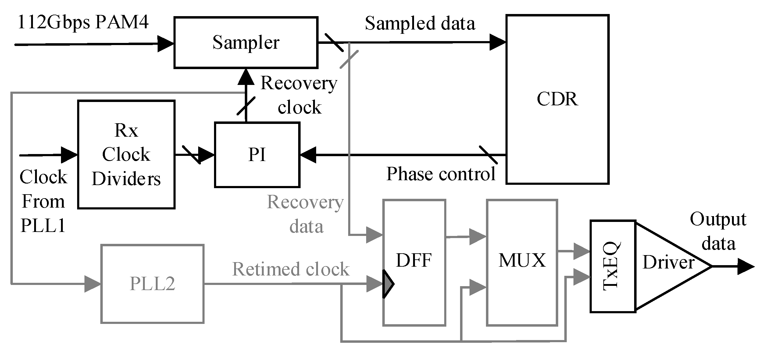
To address the key technical issues of Retimer design, this paper designs and implements a 112Gbps PAM4 low latency and low jitter Retimer circuit applied to a high-speed SerDes, with CDR, PLL, and retiming module as its main components. Its system architecture is shown in Figure 4. The input noise signal is sampled by CDR, phase tracking, phase adjustment, and the loop is locked and then the output recover the clock and recover data. However, for the 112Gbps high-speed signal, the CDR cannot effectively track on the input signal jitter, and the recovery clock quality is poor, resulting in high data BER.
The CDR recovery clock input to the PLL, filters out the high frequency jitter, and the PLL outputs a new clock signal. The new clock signal jitter performance is good to meet the high-speed signal sampling accuracy requirements. Use this clock to directly sample and combine CDR recovery data to achieve retiming of the data, and then send it out through the equalization driver. The whole process eliminates the need for time-consuming synthesizable digital logic modules, thus reducing transmission latency. This design not only eliminates the frequency difference between the sampling clock and data to ensure the quality of the sampling clock, but also reduces the signal penetration delay and achieves a low latency and low jitter retiming function.

3.2. CDR Design

In the process of designing the Retimer circuit, considering the advantages of Phase Interpolator(PI)-based CDR [11] and the characteristics of the PAM4 Baud-Rate-Phase-Detector (BRPD) [12], the BRPD-based PI type CDR is chosen in this paper.In addition, considering the frequency difference that exists in the signals at the transceiver side of the SerDes, the CDR uses a second-order digital filter to achieve stronger correction capability for phase difference and frequency difference [13].

3.2.1. Modeling Analysis and Parameter Design of CDR

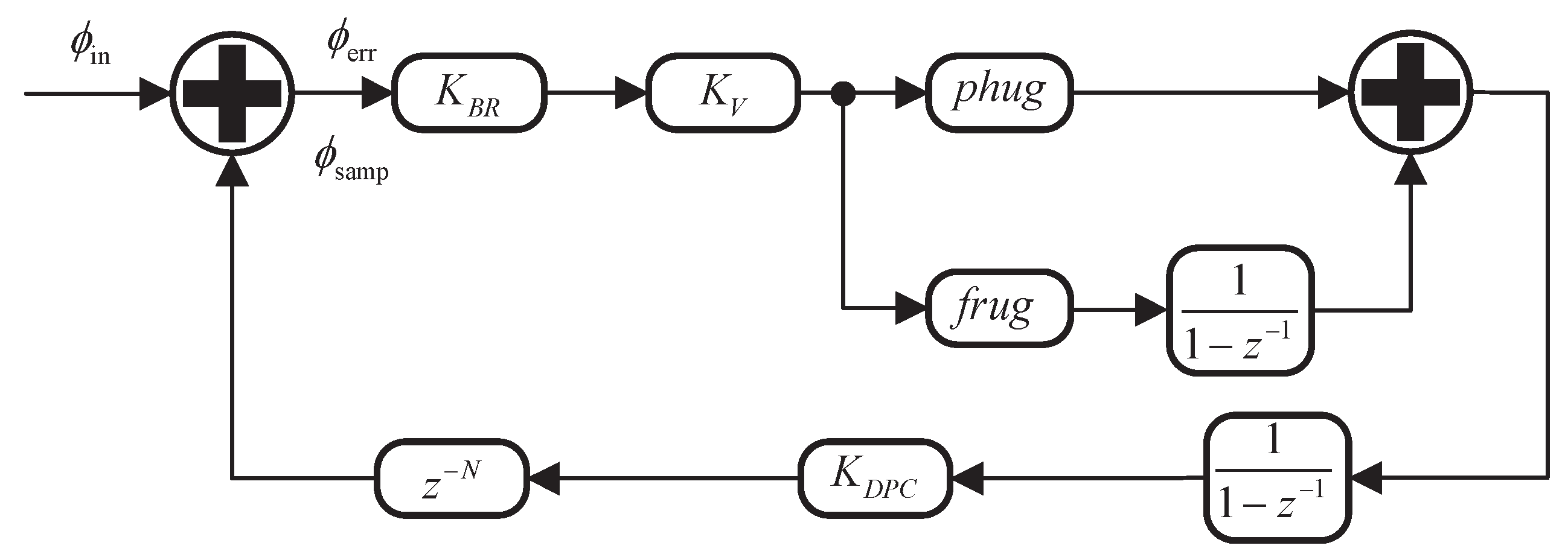
The linear model of the analog clock recovery unit is shown in Figure 5:
The loop gain of its linear system [14] is given by the following equation:
Preprints 75977 i001
Linear equivalent modeling of the CDR is performed to verify the functional correctness of the CDR circuit. The analog components in the analog charge pump phase-locked loop (CPPLL)-based CDR are replaced with digital components and converted to a digital phase-locked loop (DPLL)-based small-signal model of the CDR. the Z-domain linear equivalent model of the CDR circuit is shown in Figure 6, and the modeling approach has been provided in the literature [14].
The open-loop transfer function, closed-loop transfer function can be obtained by the equivalent model:
Preprints 75977 i002
Preprints 75977 i003
In order to be able to verify the performance of the system, the model analysis will use parameters that are consistent with the CDR in the test circuit, which are listed in Table 1 with remarks on the significance of the parameters.

3.2.2. Simulation Verification of CDR.

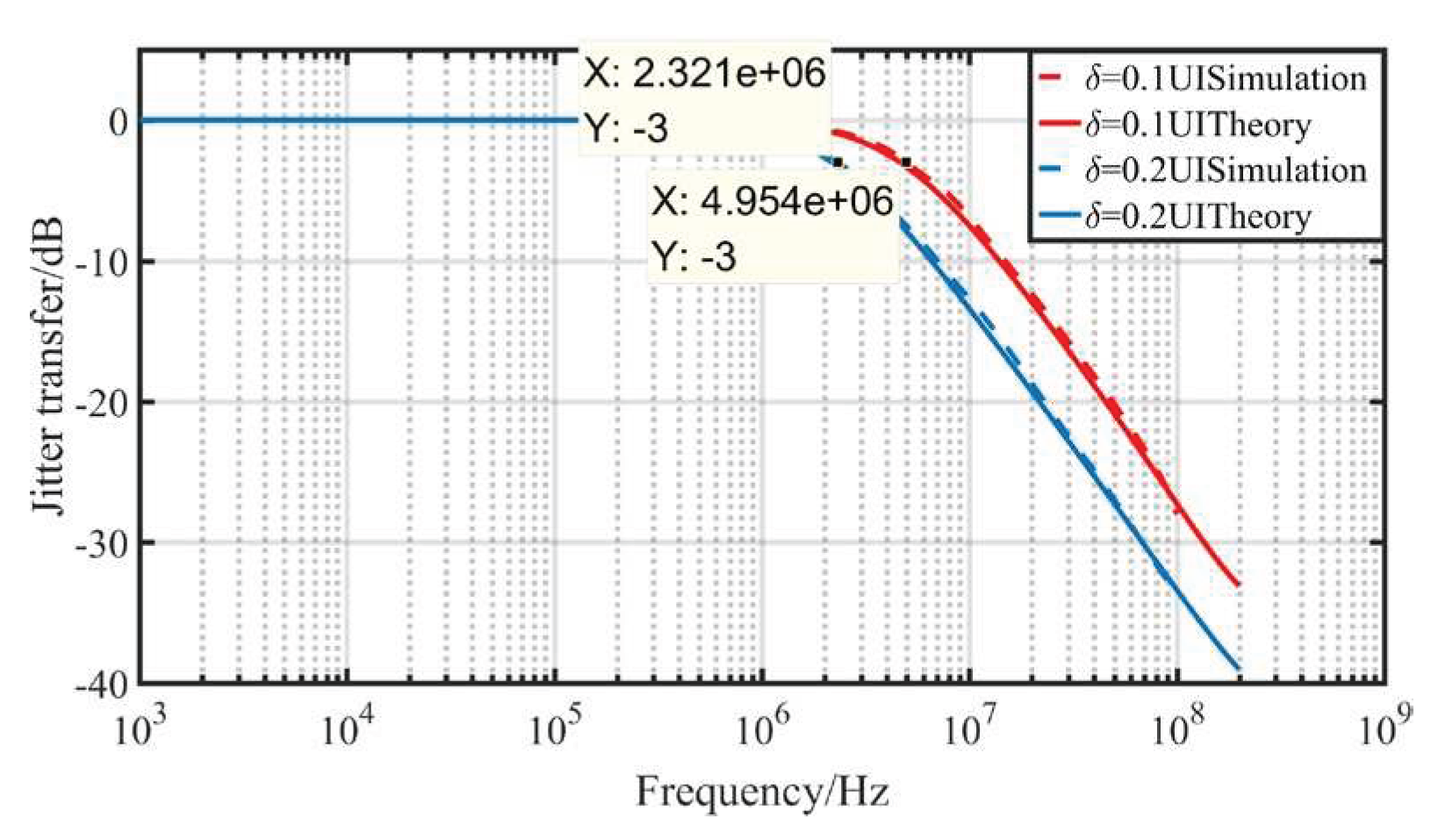
The 112Gbps PAM4 CDR circuit is simulated to verify the jitter transfer characteristics of the CDR. Figure 7 shows the theoretical and simulated jitter transfer curves of the CDR for input jitter amplitudes of 0.1UI and 0.2UI. The results show that the theoretical calculation and the simulated measurement are in good agreement, and the output jitter decays continuously when the jitter frequency exceeds ω-3dB.
Figure 8 shows the input clock and recovery clock eye diagram for jitter amplitude of 0.1UI and jitter frequencies of 1MHz, 10MHz, and 100MHz, respectively. The jitter attenuation at the three frequencies are -0.063 dB, -6.9 dB, -28.8 dB, which is basically consistent with the theoretical calculation results in Figure 6.
Figure 7 and Figure 8 show that when the jitter frequency ωp < ω-3dB, the output jitter completely tracks the input jitter and the jitter transfer is 0dB; when the jitter frequency ωp > ω-3dB, the output jitter decays at a rate of 20dB/dec.
The simulation and analysis show that the CDR can completely track the jitter on less than the loop bandwidth, and can play an obvious filtering role for the high frequency noise and jitter beyond the loop bandwidth. With the jitter amplitude of 0.1UI and 0.2UI, the CDR loop bandwidth is 4.9MHz and 2.3MHz respectively, which can verify the reasonableness of the CDR parameter setting and the correctness of the model function.

3.3. PLL Design

By introducing a jitter-canceling filtered phase-locked loop in the Retimer circuit, the jitter of the clock recovered by the CDR circuit is filtered and a high-quality retimed clock is output.

3.3.1. PLL Linear Model Analysis

The CPPLL has a wide locking range and good stability. In order to enhance the stability of the phase-locked loop system and stabilize the control voltage of the voltage-controlled oscillator, a charge-pump phase-locked loop containing a second-order loop filter is used as the filtering module of the Retimer circuit in this paper, whose linear model [15] is shown in Figure 9:
Its open-loop transfer function and closed-loop transfer function are:
Preprints 75977 i004
Preprints 75977 i005
The transfer functions of the charge pump and filter are:
Preprints 75977 i006
Preprints 75977 i007
The filter has only one zero point at ωz=1/R2C2. The voltage-controlled oscillator has one pole at the origin ωp1, and the filter introduces another origin pole ωp2 and another non-zero pole ωp3=(C1+ C2)/R2C1C2.
If the ratio of C2 and C1 is denoted by b, the relationship between the zero point and the non-zero pole is ωp3=(b+1)ωz. The phase margin of the open-loop transfer function G(jω) at any angular frequency is:
Preprints 75977 i008
The maximum value of phase margin is obtained by deriving the above equation and making it equal to 0. In order to maximize the phase margin, the phase margin maximum must be obtained at the open-loop bandwidth ω-3dB, ω-3dB = √ωzωp3, and the phase margin maximum can be obtained as:
Preprints 75977 i009
Preprints 75977 i010
Preprints 75977 i011
The non-zero poles introduced by the filter [16] increase the filtering of high frequencies on the one hand and reduce the phase margin on the other. The selection of the location of the zero and pole points has a great influence on the system stability. The article takes the values of the zero and pole points as follows: the zero point ωz is 1/4 of ω-3dB, while the non-zero pole point ωp3 is 4 times of ω-3dB, i.e., b=15. Its phase margin can be estimated as:
Preprints 75977 i012
Near the -3dB bandwidth, the filter impedance can be approximated as R2 because the integrating capacitor C2 can be regarded as a short-circuit and the pole capacitor C1 can be regarded as an open circuit. at the -3dB bandwidth, its open-loop gain is 1, that is, its forward gain is equal to the crossover ratio of the feedback divider. Thus, at the -3 dB bandwidth, we have:
Preprints 75977 i013
The -3dB bandwidth can then be expressed as:
Preprints 75977 i014
This shows that the -3dB bandwidth is independent of the value of the capacitor. At this point, the values of R2, C2 and C1 are taken as follows:
Preprints 75977 i015
Preprints 75977 i016
Preprints 75977 i017

3.3.2. PLL Parameter Design

PLL as a negative feedback system, has multiple additive noises that affect the output clock jitter throughout the circuit operation. Through [17] on the PLL multiple noise sources transmission characteristics analysis can be seen, reduce the loop bandwidth can reduce the impact of input noise, discriminating frequency discriminator and charge pump equivalent noise, loop filter noise and divider noise on the output clock signal; and increase the loop bandwidth can reduce the impact of voltage controlled oscillator on the output clock signal. Therefore, in order to obtain a low jitter output clock signal, the need for a compromise in the selection of the loop bandwidth to take the value. In this paper, according to the performance parameters of the CDR recovery clock signal, as well as the requirements of the output clock jitter of the PLL, select the value of the loop bandwidth of 0.1 MHz. combined with the theoretical calculation of the PLL linear model, determine the parameters of the PLL as shown in Table 2:
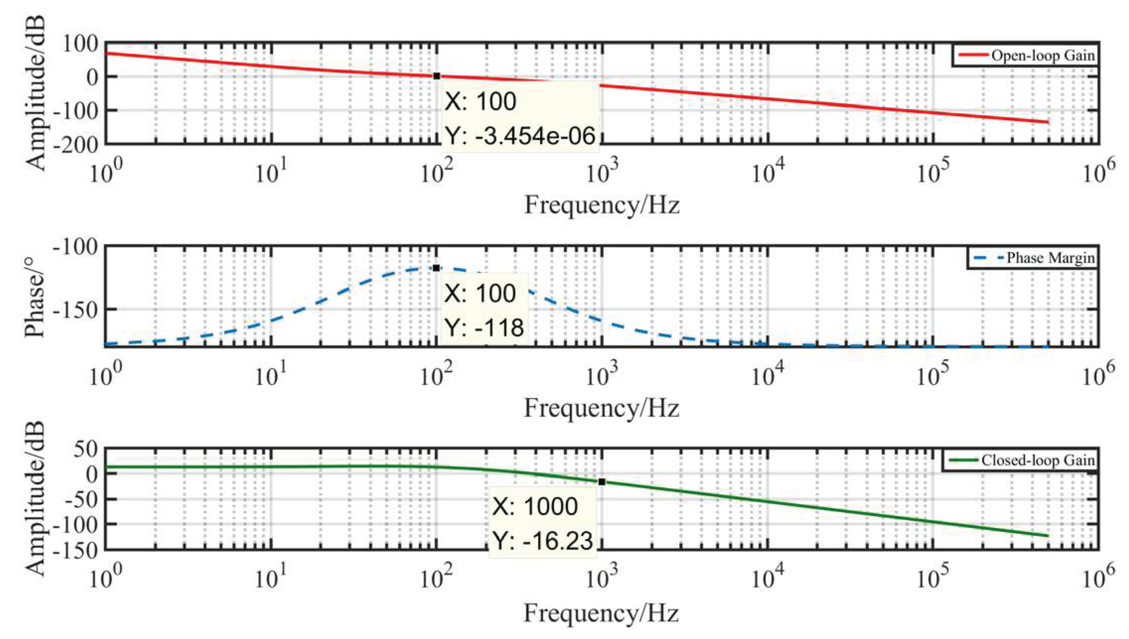
The PLL gain and phase margin are obtained by simulation, as shown in Figure 10:
Figure 10 shows that the open-loop gain of the phase-locked loop at the loop bandwidth of 0.1MHz is almost 1, when the phase margin reaches a maximum of 62°, which is consistent with the analysis in 3.3.1; the closed-loop gain of the phase-locked loop at 1MHz is -16.23dB, when the theoretical value of the output clock jitter is 554fs, and the results are verified in Section 4.

4. Retimer Circuit Simulation

The Retimer circuit designed in this paper is simulated on Cadence virtuoso (input signal is 112Gbps PAM4, sinusoidal jitter frequency is 1MHz, amplitude is 0.1UI, clock frequency is 14GHz, no frequency difference). After the Retimer circuit is locked, we can get the result of the signal penetration latency through the circuit, PLL output clock eye diagram and retiming data eye diagram at this clock.
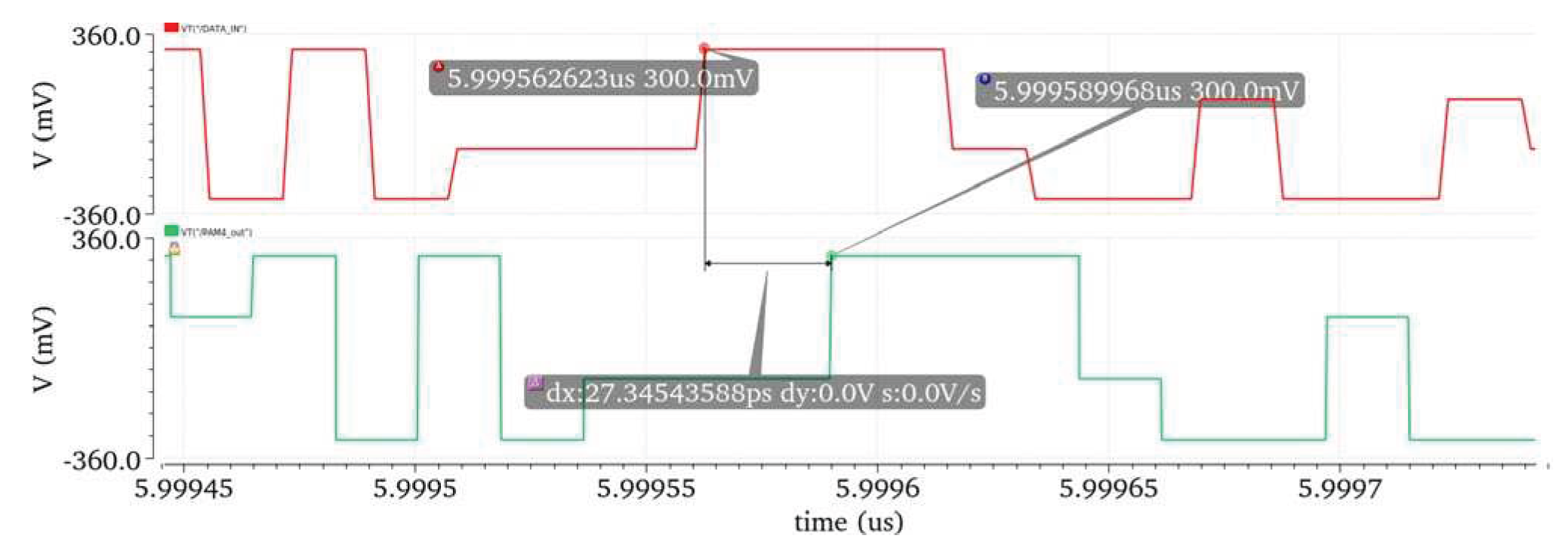
Figure 11 shows that from the time the signal is input to the Retimer circuit to the time the retiming signal is sent out, the transmission latency of the signal in the Retimer circuit is 27.3ps, which is 83.5% lower than that of the conventional Retimer circuit.
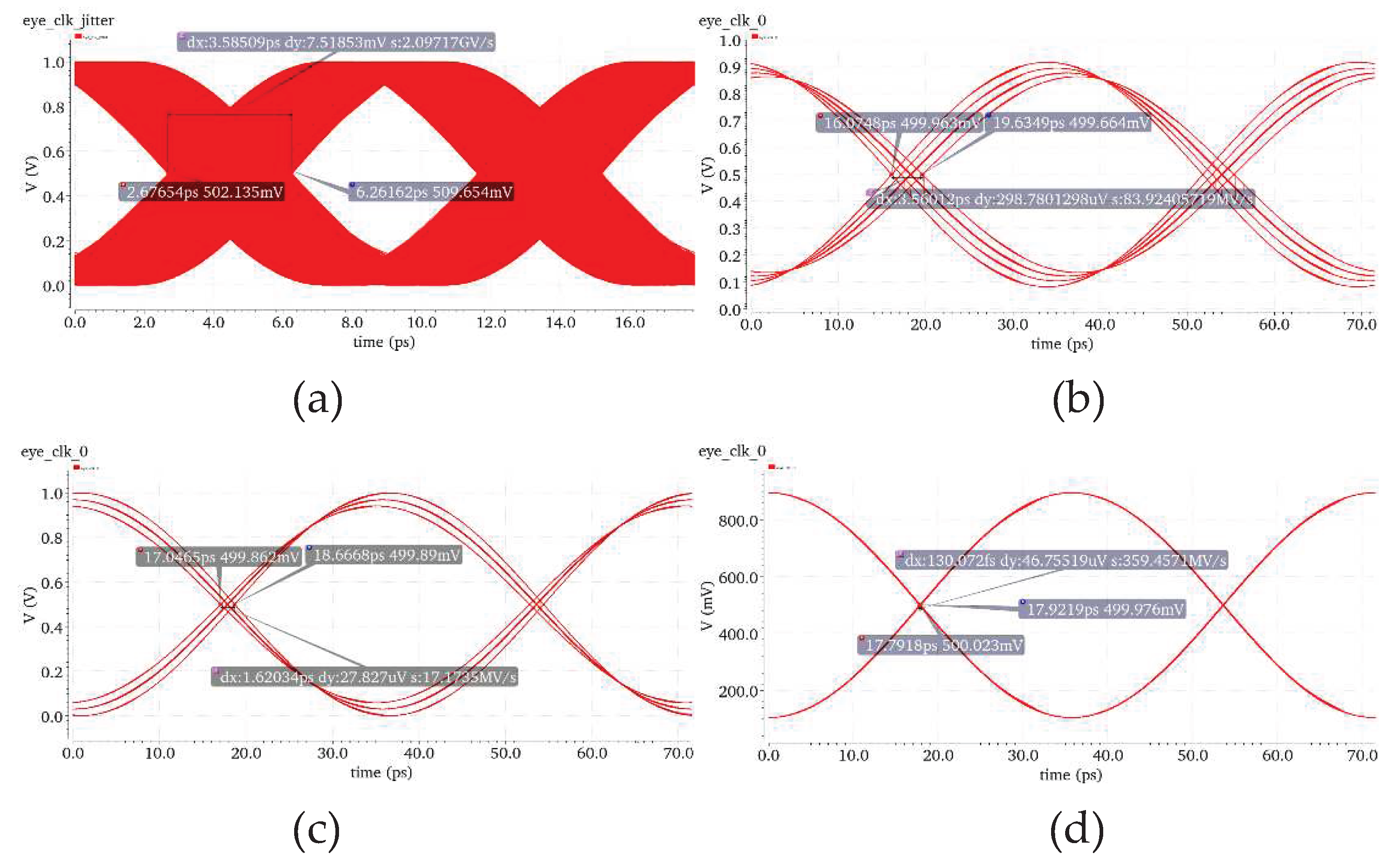
As in Figure 12, by observing the eye diagram of the PLL output clock after Retimer lock and the retimed data under this clock, it can be found that the PLL output clock jitter is 600.8 fs, compared with the input clock jitter of 3.57 ps, the jitter is attenuated by -15.5 dB, which verifies the theoretical value in Figure 10; the jitter of retimed data is 741 fs, which is 31.4% lower compared to the jitter of retimed data of conventional Retimer circuit.
Table 3 shows the results of the comparison between the Retimer designed in this paper and the conventional Retimer.
The simulation results illustrate that the Retimer circuit based on CDR+PLL architecture designed in this paper has good jitter performance and latency performance, and also shows the rationality of the analysis and parameter design of the CDR and PLL system in this paper.

5. Conclusions

In this paper, a Retimer circuit based on CDR+PLL architecture is proposed for PCIe 6.0 to address the problems of high speed Retimer circuit with large penetration delay and low jitter performance. By connecting the PLL circuit at the back end of CDR, the clock signal containing large jitter recovered from CDR is input to the PLL for high-frequency filtering, and a low-jitter retiming clock is obtained, and then the CDR recovery data is sampled and combined and sent, which reduces the signal penetration delay while reducing the output data jitter. This study provides a new design architecture for high-speed Retimer and provides technical support for enhancing the overall performance of PCIe 6.0.

Author Contributions

Conceptualization, H.W. and F.L.; methodology, Q.L., G.Z. and D.L.; software, Q.L., H.W. and G.Z.; validation, Q.L. and D.L.; resources, F.L.; formal analysis, Q.L. and D.L.; data curation, Q.L.; writing—original draft preparation, Q.L. and H.W.; writing—review and editing, H.W.; funding acquisition, F.L. All authors have read and agreed to the published version of the manuscript.

Funding

This research was funded by National Key R&D Program (2022YFB2803101).

Conflicts of Interest

The authors declare no conflict of interest.

References

  1. Chang, F.L.; Amber, T.; Arun, T.; et al. 6.5 A 400Gb/s Transceiver for PAM-4 Optical Direct-Detect Application in 16nm FinFET. In Proceedings of the 2019 IEEE International Solid- State Circuits Conference (ISSCC), San Francisco, CA, USA, 2019, pp. 120-122. [CrossRef]
  2. Robert, R.; Michael, R.; Fran, K.; et al. A 4.5 mW/Gb/s 6.4 Gb/s 22+1-Lane Source Synchronous Receiver Core with Optional Cleanup PLL in 65 nm CMOS. In Proceedings of the 2010 IEEE Journal of Solid-State Circuits (JSSC), Dec. 2010, vol. 45, no. 12, pp. 2850-2860. [CrossRef]
  3. Hiok-Tiaq Ng; Ramin, F.R.; William, J.D.; et al. A second-order semidigital clock recovery circuit based on injection locking. In Proceedings of the 2003 IEEE Journal of Solid-State Circuits (JSSC), Dec. 2003, vol. 38, no. 12, pp. 2101-2110. [CrossRef]
  4. Tamer, A.; Robert, D.; Ron, H.; Chih-Kong, K. Y.; A 100+ Meter 12 Gb/s/Lane Copper Cable Link Based on Clock-Forwarding. In Proceedings of the 2013 IEEE Journal of Solid-State Circuits (JSSC), April 2013, vol. 48, no. 4, pp. 1085-1098. [CrossRef]
  5. Yasuhiro, N.; Toshihide, S.; Hideki, K.; et al. A 43-Gb/s full-rate-clock 4:1 multiplexer in InP-based HEMT technology. In Proceedings of the 2002 IEEE Journal of Solid-State Circuits (JSSC), Dec. 2002, vol. 37, no. 12, pp. 1703-1709. [CrossRef]
  6. S. Hu; et al. A 50Gb/s PAM-4 Retimer-CDR + VCSEL Driver with Asymmetric Pulsed Pre-Emphasis Integrated into a Single CMOS Die. 2019 Optical Fiber Communications Conference and Exhibition (OFC), San Diego, CA, USA, 2019, pp. 1-3.
  7. T. Tang; B. Wray; R. Murugan; Die-Package-PCB Signal Integrity Performance Debug of a High-Speed (25Gbps) Retimer: Simulation to Measurement Correlation. 2020 IEEE International Symposium on Electromagnetic Compatibility & Signal/Power Integrity (EMCSI), Reno, NV, USA,2020, pp.170-175. dio: 10.1109/EMCSI38923.2020.9191568.
  8. P. Mishra; A. Tan; B. Helal; et al. A 112Gb/s ADC-DSP-Based PAM-4 Transceiver for Long-Reach Applications with >40dB Channel Loss in 7nm FinFET. In Proceedings of the 2021 IEEE International Solid- State Circuits Conference (ISSCC), San Francisco, CA, USA, 2021, pp. 138-140. doi: 10.1109/ISSCC42613.2021.9365929.
  9. Zhao, L.W. The low latency of data transmission design based on FPGA. Master’s Degree Thesis, Zhengzhou University, Zhengzhou, China, 2017. https://kns.cnki.net/KCMS/detail/detail.aspx?dbname=CMFD201702&filename=1017128975.nh.
  10. Wang, C. Design and implementation of Low-Latency error correction coding for Ultra-High-Speed interconnection transmission Links. Master’s Degree Thesis, National University of Defense Technology, Changsha, China,2020. [CrossRef]
  11. GUO, K.L.; WANG, H.M.; LIU, T.; et al. A Non - Equivalent Tail Current Source Based New Phase Interpolator with High Linearity for High - Speed SerDes. Journal of Air Force Engineering University (Natural Science Edition), 2020, vol. 21, no. 4, pp. 61 – 67. [CrossRef]
  12. Li, T.J.; Zhang, G.; Zhang, J.M.; Xin, K.W. A Novel High-Gain PAM4 Baud-Rate Phase Detector for ADC-Based CDR. 2022 7th International Conference on Integrated Circuits and Microsystems (ICICM), Xi’an, China, 2022, pp. 606-609. [CrossRef]
  13. Luan, W.H.; Wang, D.J.; Jia, Chen. Modeling Analysis and Circuit Design of Second-Order Clock Data Recovery Circuit Applied to 10 Gbase-KR. Microelectronics and Computers ,2020, vol. 37, no. 03, pp. 1-4. [CrossRef]
  14. Jeff, L.S.; John, S. A digital clock and data recovery architecture for multi-gigabit/s binary links. Proceedings of the IEEE 2005 Custom Integrated Circuits Conference (CICC), San Jose, CA, USA, 2005, pp. 537-544. [CrossRef]
  15. Xin, K.W.; Lyu, F.X; Wang, J.Y. A Low Noise Clock Generator for High-Speed Serial Interface. Microelectronics, 2019, vol. 49, no. 06, pp. 817-823. [CrossRef]
  16. Zhang, G. Design of COMS Integrated Phase Locked Loop Circuit. First Edition, Tsinghua University Press, Beijing, China,2013. pp. 15–17.
  17. Yang, C. Research and design of fast-locked, high-speed and low-jitter clock generation. Master’s Degree Thesis, University of Electronic Science and Technology of China, Chongqing, China,2015.
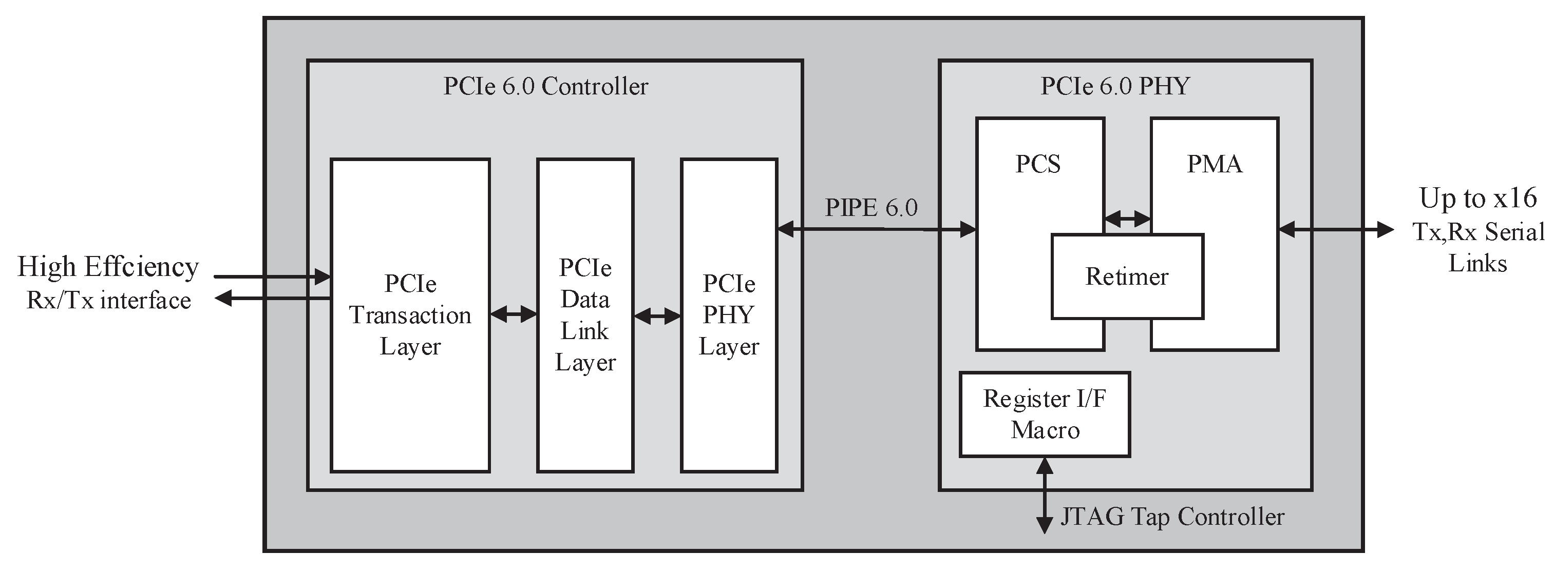
Figure 1. PCIe 6.0 Interface Subsystem.
Preprints 75977 g001
Figure 2. The conventional Retimer circuit structure.
Preprints 75977 g002
Figure 3. (a) Signal Penetration latency from input to output; (b)The output signal eye Diagram.
Preprints 75977 g003
Figure 4. The Retimer circuit architecture proposed in this article.
Preprints 75977 g004
Figure 5. The linear model of the analog clock recovery unit.
Preprints 75977 g005
Figure 6. The Z-Domain linear equivalent model of CDR circuit.
Preprints 75977 g006
Figure 7. The jitter transmission characteristics of CDR.
Preprints 75977 g007
Figure 8. (a) Input clock eye diagram; (b) Recovery clock eye diagram (jitter amplitude 0.1UI, jitter frequency 1M) ; (c) Recovery clock eye diagram (jitter amplitude 0.1UI, jitter frequency 10M) ; (d) Recovery clock eye diagram (jitter amplitude 0.1UI, jitter frequency 100M) .
Preprints 75977 g008
Figure 9. The CPPLL S-Domain linear model.
Preprints 75977 g009
Figure 10. PLL gain and phase margin.
Preprints 75977 g010
Figure 11. Retimer circuit transmission latency.
Preprints 75977 g011
Figure 12. (a) PLL Recovery Clock Eye Diagram; (b) Retiming data.
Preprints 75977 g012
Table 1. CDR Design Parameters.
CDR Parameters Design Value
PD gain (KBR) 0.56
Voting gain (KV) 0.54*64=19.2
Proportional path gain (phug) 1
Integral path gain (frug) 2-14
Digital phase converter gain (KDPC) 2-9
Loop latency (N) 4
Table 2. PLL Design Parameters.
PLL Parameters Design Value
Charge pump current (IP) 0.15mA
Filter capacitance (C1) 2.2616nF
Filter capacitance (C2) 34.119nF
Filter resistance (R2) 187.09Ohms
VCO gain (KVCO) 600MHz/V
Divider (N) 4
Table 3. Results of this paper’s Retimer versus conventional Retimer.
Parameters Conventional Retimer This paper Retimer
Main structural features CDR+DFF CDR+PLL+PLL
Retiming data jitter 1.08ps 0.741ps
Data jitter attenuation -10.38dB -13.66dB
Penetration latency 165.3ps 27.3ps
Disclaimer/Publisher’s Note: The statements, opinions and data contained in all publications are solely those of the individual author(s) and contributor(s) and not of MDPI and/or the editor(s). MDPI and/or the editor(s) disclaim responsibility for any injury to people or property resulting from any ideas, methods, instructions or products referred to in the content.
Copyright: This open access article is published under a Creative Commons CC BY 4.0 license, which permit the free download, distribution, and reuse, provided that the author and preprint are cited in any reuse.
Prerpints.org logo

Preprints.org is a free preprint server supported by MDPI in Basel, Switzerland.

Subscribe

© 2024 MDPI (Basel, Switzerland) unless otherwise stated