
Submitted:
17 February 2023
Posted:
17 February 2023
You are already at the latest version
Abstract
Deep-ultraviolet (UV) light-emitting diodes (LEDs) based on AlGaN crystals have low light-emission efficiency; therefore, there is a need to improve this light-emission efficiency for a wide range of applications such as water and air sterilizations. UV-light-transparent device structures are considered one of the many solutions toward increasing light output power. To this end, the present study focused on developing a transparent AlGaN-based tunnel junction (TJ) as the anode of a deep-UV LED. Deep-UV LEDs composed of n+/p+-type AlGaN TJs were fabricated under the growth condition that reduced the carrier compensation in the n+-type AlGaN layers. The operating voltage was 10.8 V under the direct current (DC) operation of 63 A/cm2. In addition, magnesium zinc oxide (MgZnO)/Al reflective electrodes were fabricated to enhance the output power of the AlGaN homoepitaxial TJ LED. The output power was 57.3 mW under a DC operation of 63 A/cm2, and it was 1.7 times higher than that realized using the conventional Ti/Al electrodes. The combination of the AlGaN-based TJ and MgZnO/Al reflective contact allows further improvement of the light output power. This study confirms that the AlGaN TJ is a promising UV-transmittance structure that can obtain a high light-extraction efficiency.
Keywords:
AlGaN
; tunnel junction
; light-emitting diode
; deep-ultraviolet
; MgZnO
1. Introduction
Aluminum gallium nitride (AlGaN)-based light-emitting diodes (LEDs) emit deep-ultraviolet (UV) light and are utilized in several applications at different wavelengths such as in curing, sensing, and water and air sterilizations. These LEDs are considered replacements for the mercury lamps used in water and air sterilizations [1,2,3]. Deep-UV light with an emission wavelength below 290 nm can rapidly inactivate the deoxyribonucleic acid of virus and bacteria [4,5]; however, the light-emission efficiency (LEE) of deep-UV LEDs is considerably lower than that of low-pressure mercury lamps. The wall-plug efficiency of mass-produced deep-UV LEDs is a maximum of 10% because of the UV light absorption of the p-type gallium nitride (GaN) contact layer [6,7,8]. A p-type GaN contact layer is used in mass-produced deep-UV LEDs because a higher Al composition p-type AlGaN can lead to a higher ionization energy of magnesium (Mg) acceptors and a lower hole concentration [9,10,11,12,13,14]. Deep-UV LEDs with p-type AlGaN contact layers exhibited external quantum efficiencies (EQEs) of 10%–20% when rhodium (Rh) electrodes, patterned sapphire substrates, and resin encapsulations were used [15,16]. However, the wall-plug efficiencies (WPEs) of these deep-UV LEDs were not still high because of the increased contact resistivities between the electrodes and p-type AlGaN contact layers. By contrast, suitable electrode materials such as vanadium are available for n-type AlGaN-based cathode contacts [17,18,19].
One solution to this problem is forming a tunnel junction (TJ) for the anode contact of a deep-UV LED, because an n-type electrode with a low contact resistance is available. Table 1 lists previously reported LEDs having TJ-based anode contacts [20,21,22,23,24,25,26,27,28,29,30,31]. Some issues are faced in realizing a TJ-LED with a high-Al composition. The first issue is the difficulty of dehydrogenation from the buried p-type III-nitride layers. When using metalorganic vapor phase epitaxy (MOVPE) growth that is suitable for manufacturing LEDs, Mg acceptors are passivated by the hydrogen atoms in the growth ambient, resulting in a high resistivity [32,33]. Then, hydrogen atoms mostly locate at interstitial sites in III-nitrides [14]. An interstitial hydrogen atom is predicted to be charged positively and to be mobile in the p-type layer, whereas it would have a negative charge and be less mobile in the n-type layer [34]. Dehydrogenation from the p-type GaN layer buried under the n-type GaN has been reported to be difficult [35]. To avoid this problem, TJ layers were grown in the hydrogen-free ambient by methods such as plasma-enhanced molecular beam epitaxy (PAMBE) [20,22,26,27,28,29,30] as it results in a lower differential specific resistivity (Rs) compared with that in the case of conventional MOVPE growth [21,23,24,25,31]. Recently, Akasaka et al. demonstrated the low resistivity of the n+-type GaN/p+-type GaN TJ using MOVPE growth by optimizing the doping profile and growth condition [25]; this should contribute toward the manufacture of GaN-based TJ contacts.
The second issue is the fact that the formation of highly-conductive TJs is more challenging for AlGaN-based TJs than for GaN-based ones, as seen from Table 1. This is caused by the increased tunneling barrier when the Al content increases. Deep-UV LEDs having AlGaN-TJ anode contacts reportedly enhanced the LEE; specifically, the LEE was high, and the operation voltages remained high in the range of 13–50 V [30,31]. To enhance the conductivity of the anode contact, Zhang et al. reported TJ double-heterostructures comprising n+-AlGaN/(Ga)InN/p+-AlGaN, in which the polarization charges reduced the TJ thickness [26,27,28]. The integration with the polarization doping technique using a graded AlGaN TJ layer was also effective in attracting high density free holes, resulting in enhanced tunneling probability [26].
A simpler way to increase the tunneling probability is to increase the doping concentration of tunneling homojunction layers. However, the resistivities of high-Al-content n-type AlGaN layers with high Si-doping concentrations (>6 × 1019 cm−3) were found to be extremely high because of the self-compensation caused by cation–vacancy–silicon (VIII–nSi) complexes [32,33,34,35,36,37,38,39,40,41]. Further, carbon atoms were reported to cause carrier compensation by substituting nitrogen sites (CN) and to reduce the conductivities of n-type GaN layers [42,43,44,45]. The similar carrier compensation via CN was predicted for an AlN-based material [46]. The growth condition of the high-Si-doped n+-type AlGaN needs to be controlled for suppressing the carrier compensation defects and reducing the operating voltage of AlGaN TJ LEDs.
The design of the electrode structure for light extraction from the backside is also important for deep-UV LEDs [47,48]. The output power can be enhanced using a high reflective electrode on the top. In visible-light LEDs, highly reflective metals combined with UV-transparent and conductive oxide electrodes are widely used to improve the LEE [49,50]. Examples of such oxide elements include indium tin oxide [51,52], indium-doped zinc oxide [53,54,55], aluminum-doped zinc oxide [56,57,58], and gallium-doped zinc oxide [59,60]. High reflective electrodes can be produced by stacking Al metals or a distributed Bragg reflector on these oxide electrodes, resulting in a reflectivity of 80%–90% [49,50]. Visible-light LEDs with high LEE can also be obtained by applying these reflective structures. However, these oxide materials have an absorption deep-UV region owing to bandgap energies of 3.34–4.3 eV. We focus on high-Al composition AlGaN TJ LEDs and magnesium zinc oxide (MgZnO)/Al reflective electrode. An MgZnO is suitable for suppressing the UV light absorption, and its bandgap can be controlled in the range of 3.34 to 7.8 eV by controlling the Mg/Zn composition [61,62]. A previous study reported that the MgZnO formed by the sputtering had two crystalline structures after recrystallization by annealing; both structures exhibited high transmittance in the UV range and n-type conductivity [63]. The conductivity was improved because of the mixture of both wurtzite structure MgZnO and rock salt structure or the oxygen vacancies in wurtzite structure MgZnO. The resistivity and transmittance of MgZnO were 1.1×10⁻¹ Ωcm and 20%, respectively [63]. There have been reports of improving the LEE of UV-A LEDs using MgZnO [64,65], but there have been no reports of UV-C LEDs.
In this study, we review the key challenges faced in deep-UV LEDs with AlGaN-based TJ anode contacts. The growth conditions of the n+-type AlGaN of TJ are controlled such that carbon incorporation can be suppressed at high Si doping to reduce the operating voltage of the AlGaN TJ LED. Further, we demonstrate that MgZnO/Al reflective electrodes can fully exploit the transparent structure of TJs, which results in enhancing the LEE of deep-UV LEDs.

Table 1.
Summary of the III-nitride TJs reported previously, where VF is a forward operation voltage and Rs is a differential specific resistivity.
Table 1.
Summary of the III-nitride TJs reported previously, where VF is a forward operation voltage and Rs is a differential specific resistivity.
| Ref. | TJ structure | Growth method | VF (V) | Rs (Ωcm2) |
| [20] | n+-GaN/GaInN/p+-GaN | PAMBE | 3.05 @100 A/cm2 | 1.2 × 10⁻⁴ |
| [21] | n+-GaN/p+-Ga0.6In0.4N | MOVPE | 4.0 × 10⁻³ | |
| [22] | n+-GaN/p+-GaN | MOVPE+NH3-MBE | ~5 @100 A/cm2 | 2.3 × 10⁻⁴ |
| [23] | n+-GaN/p+-GaN | MOVPE | 5.92 @2 A/cm2 | 2.6 × 10⁻¹ |
| [24] | n+-GaN/p+-GaN µ-LED | MOVPE | ~4 @20 A/cm2 | 2.5 × 10⁻⁵ |
| [25] | n+-GaN/p+-GaN | MOVPE | ~4 @100 A/cm2 | 2.4 × 10⁻⁴ |
| [26] | n+-Al0.55Ga0.45N/ Ga0.8In0.2N /p+-Al0.55Ga0.45N |
PAMBE | 6.8 @10 A/cm2 | 1.5 × 10⁻³ |
| [27] | n+-AlGaN/ Ga0.8In0.2N /graded p-AlGaN |
PAMBE | 10.2 @10 A/cm2 | N/A |
| [28] | graded n+-AlGaN / Ga0.8In0.2N/p+-Al0.65Ga0.35N |
PAMBE | 10.5 @20 A/cm2 | 1.9 × 10⁻³ |
| [29] | n+-Al0.65Ga0.35N/GaN /p+-Al0.65Ga0.35N |
PAMBE | ~10 @100 A/cm2 | N/A |
| [30] | n+-Al0.5Ga0.5N/GaN /p+-Al0.5Ga0.5N |
MOVPE+NH3-MBE | ~9 @100 A/cm2 | 1.2 × 10⁻³ |
| [30] | n+-Al0.5Ga0.5N/p+-Al0.5Ga0.5N | MOVPE+NH3-MBE | ~11 @100 A/cm2 | 1.7 × 10⁻³ |
| [31] | n+-Al0.65Ga0.35N/n+-GaN /p+-Al0.65Ga0.35N |
MOVPE | ~20 | (4-6) × 10-3 |
| [31] | n+-Al0.65Ga0.35N /p+-Al0.65Ga0.35N |
MOVPE | ~50 | N/A |
2. Materials and Methods
Deep-UV LEDs were grown using a metalorganic vapor phase epitaxy on c-plane sapphire substrates with a miscut angle of 0.35° toward the sapphire [110] direction. Trimethylaluminium, trimethylgallium, triethylgallium, Bis(cyclopentadienyl)magnesium, monosilane gas, and ammonia gases were used as Al, Ga, Mg, Si, and N sources under hydrogen gas, respectively. The sapphire substrates were thermally cleaned in the H2 ambient, and then, a 3-μm-thick AlN was grown using a two-step growth technique [66]. Threading dislocation densities of screw and edge dislocations including mixed components in the AlN underlayer were estimated using an X-ray rocking curve at 9 × 107 cm−2 and 1 × 109 cm−2, respectively [67]. The 1.3-μm-thick n-type Al0.62Ga0.38N doped with a Si concentration of 3 × 1019 cm−3 was grown on an AlN template [40,41]. Multiple-quantum wells, an Al0.85Ga0.15N electron blocking layer (EBL), a p-type AlGaN, and a p+-type AlGaN were grown on the n-type AlGaN underlayer. The p+-type AlGaN was doped with Mg at a concentration of 1.7 × 1020 cm−3. Subsequently, n+-type and n-type AlGaN were grown under the same conditions as those of the n-type AlGaN underlayer, as indicated in Figure 1(b). The mesa was formed by dry etching using HCl gas. Thereafter, we formed 20/150/50/100/240-nm-thick V/Al/Ti/Pt/Au electrodes as both n-type AlGaN electrodes, and they were simultaneously annealed under a nitrogen (N2) ambient at 720 °C for 30 s. Further, the annealing process contributes Mg activation under lateral hydrogen diffusion from the exposed mesa-parts of the p-type layers [30,31,68–70]. For comparison, we prepared a conventional pn-diode-based LED with a thin p-type GaN contact layer grown on a p-type AlGaN shown in Figure 1(a). We adopted indium zinc oxide (IZO) for the anode. The emitted UV light was fully absorbed at the IZO electrode; the sizes of the LED and the anode, and the thickness of the sapphire substrate were 1 mm2, 0.56 mm2, and 200 μm, respectively. The light output power was measured using an integrating sphere. For the former, we prepared an AlGaN homoepitaxial TJ LED (TJ#1 to TJ#5) with various Si concentrations and C incorporations in the n+-type AlGaN layer, as summarized in Table 2 [71]. The carbon concentration was approximately 3.0 × 1018 cm−3 (TJ#1 and TJ#2), and it was reduced to 6.5 × 1017 cm−3 (TJ#3 to TJ#5) by changing the growth pressure from 50 mbar to 100 mbar. In case of the latter, we prepared MgZnO/Al electrodes for the TJ LED with TJ#5. We deposited a 50-nm-thick MgZnO electrode by RF magnetron sputtering at a substrate temperature of 200 °C, and a typical lift-off process was employed. The sputtering target for MgZnO was prepared as a 2-inch MgZnO sintered material of purity 4N, which is the MgO:ZnO mixing atomic ratio of 1:2. The RF power, sputtering gas, and gas pressure were 100 W, Ar, and approximately 3.4–3.5 × 10⁻¹ Pa, respectively. After forming the MgZnO electrode, the conductivity was improved by annealing at 850 °C for 5 min under N2 ambient. In the cathode, Ti/Al electrodes were deposited by the electron beam (EB) method and alloyed at 450 °C under N2 ambient. Al/Ti/Pt/Au electrodes with 300/50/100/240 nm were formed on the MgZnO electrode via the EB method to obtain a high-reflective electrode. The reflectance of the electrodes for TJ LEDs was measured using a UV-visible spectrophotometer (UV-VIS). For comparison, Ti/Al electrodes for the TJ LED anode were prepared via the same process as the cathode.
3. Results and Discussions
3.1. AlGaN homoepitaxial tunnel-junction deep-UV LEDs with n-type AlGaN based on suppressed complex defect formation
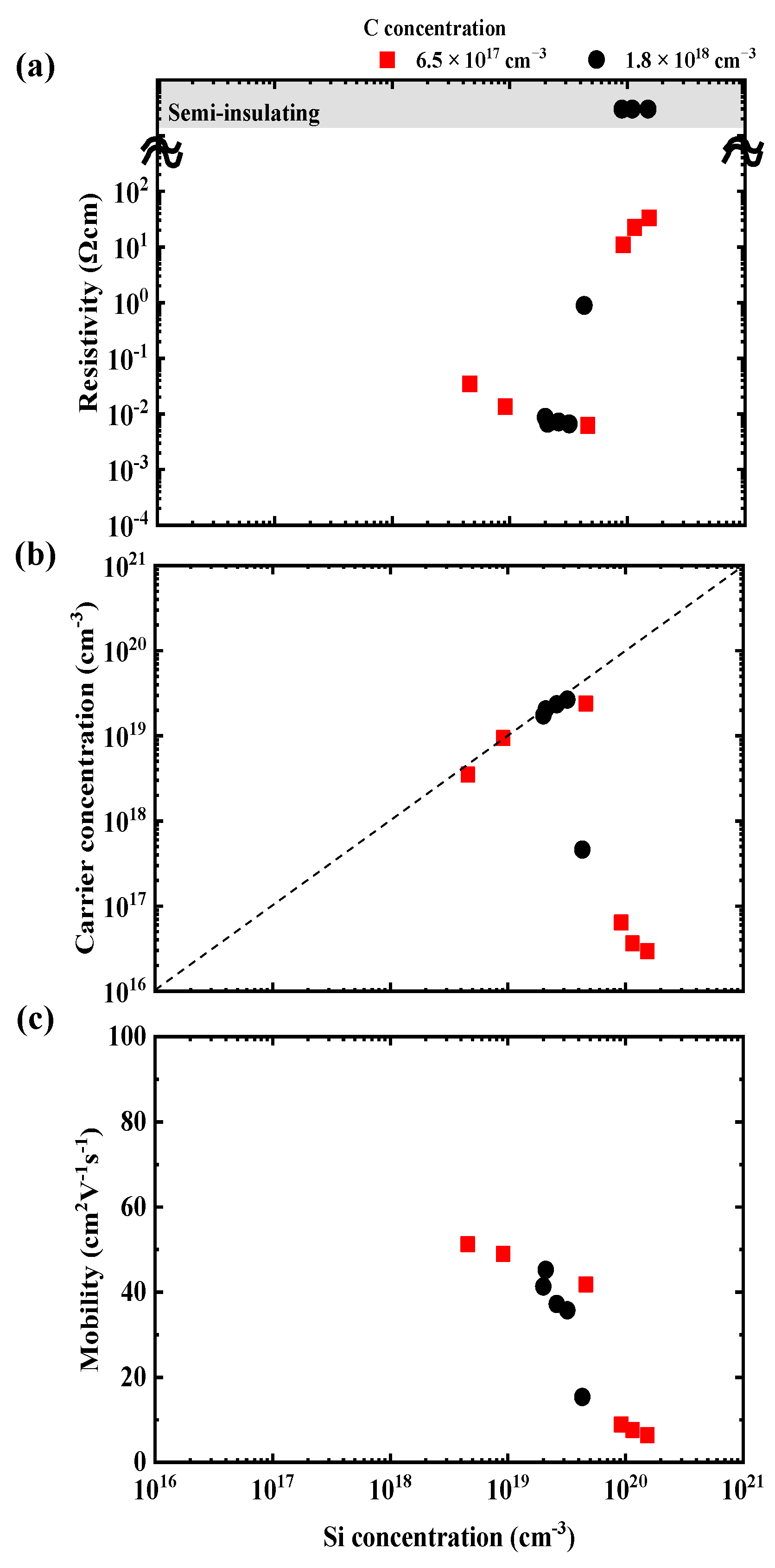
Forward voltage–current density characteristics for samples PN#1, TJ#1, TJ#2, TJ#3, and TJ#4 are presented in Figure 2 and measured by direct current (DC) operation at 300 K. The forward voltage (6.6 V) of the conventional PN LED (PN#1) was provided at 63 A/cm2. The characteristics were roughly the same as those reported previously [16,72,73]. The forward voltage of the TJ LEDs (TJ#1 and TJ#2) was extremely high and operated at approximately 16 V at 4 A/cm2. These TJ LEDs could not perform sufficient current injection; however, a slightly decreasing forward voltage trend was observed for TJ#2 relative to TJ#1. Forward voltages of TJ#3 and TJ#4 were 12.1 V and 10.3 V at 63 A/cm2, respectively, and this was significantly reduced by more than 6 V than those of TJ#1 and TJ#2. The high-doping Si concentration of the n+-type AlGaN was effective in reducing the forward voltage of the AlGaN TJ LEDs. Further, suppressing the C incorporation was more effective than the high Si-doping concentration of the n+-type AlGaN in reducing the forward voltage. The operating voltage of AlGaN TJ LEDs could be reduced because the carrier concentration of n+-type Al0.6Ga0.4N was increased by suppressing the C incorporation. The electrical characteristics of the n-type AlGaN at 300 K under the van der–Pauw Hall effect were measured. The carrier concentration and resistivity of the n+-type Al0.6Ga0.4N with a Si concentration of 1.2 × 1020 cm−3 based on TJ#2 was extremely low (< 1.0 × 1016 cm-3) and semi-insulating because of the compensation by CN, as shown in Figure 3 (a) and ref. [68]. Those at a Si concentration of 1.2 × 1020 cm−3 based on TJ#4 were 3.5 × 1016 cm−3 and 23 Ωcm, respectively, because of the suppression of C incorporation in the n+-type AlGaN. This improvement contributes to the reduction in the forward voltage for TJ#4 compared to TJ#2.
The difference in the forward voltages between TJ#3 and TJ#4 suggests that the Si overdose above 6 × 1019 cm−3 is effective for improving TJ despite the reduction in the carrier concentration with an increase of Si concentration, as shown in Figure 3(b). The reduction of the carrier concentration can be attributed to the self-compensation of VIII–nSi complexes [32,33,34,35,36,37,38,39,40,41]. However, the depletion layer width was found to be reduced to approximately 10 nm for the Si doping concentration of 1.2 × 1020 cm−3 [74]. Therefore, the Si overdose can contribute to a reduction in the depletion layer width, which results in an increase in the tunneling probability. Another possibility is trap-assisted tunneling through defects formed by the Si overdose although a further investigation is required. Therefore, we concluded that both the C reduction and high Si doping are keys to reduce the forward voltage of AlGaN-based TJs.
The present TJ structure has very thick TJ layer compared to the depletion layer width of approximately 10 nm shown in Figure 1(b), and it can be a cause of the excess series resistance of the n+-type AlGaN layer. We further reduce the operation voltage to 8.8 V at a DC current of 63 A/cm2 by optimizing the TJ thickness [75].
Figure 3.
Si concentration dependence of (a) resistivity, (b) carrier concentration, and (c) mobility of n-type Al0.62Ga0.38N. The red square (■) and black circle (●) represent the values of C concentrations of 1.8 × 1018 cm−3 and 6.5 × 1017 cm−3, as grown under pressures 50 mbar and 100 mbar, respectively.
3.2. Sputtered polycrystalline MgZnO/Al reflective electrodes for enhanced light emission in AlGaN-based homoepitaxial tunnel junction DUV-LED
We evaluate MgZnO/Al reflective electrodes for an Al0.6Ga0.4N TJ LED (TJ#5) to enhance the LEE. The TJ LED of TJ#5 is performed under the optimized growth condition similar to that of TJ#4. These forward voltages are slightly increased by approximately 0.6 V when the Al composition of the p-type AlGaN increased from 50% (TJ#4) to 60% (TJ#5).
The current density–forward voltage characteristics of the AlGaN TJ LEDs using conventional Ti/Al and MgZnO electrodes are illustrated in Figure 4(a). The forward voltages of the AlGaN TJ LEDs using Ti/Al and MgZnO/Al electrodes were 10.8 V and 10.3 V at a DC operation of 63 A/cm2, respectively. The forward voltage offset of approximately 1 V was observed for the AlGaN TJ LED using MgZnO/Al electrodes compared with that using the Ti/Al electrodes at a current density of 30–60 A/cm2. In addition, the forward voltages of the TJ LEDs of both Ti/Al and MgZnO/Al electrodes are comparable at a current density above 30 A/cm2. Therefore, we realized carrier injection into the TJ LED using MgZnO/Al electrodes. For more details, the contact resistivity and band alignment of the interface between the MgZnO electrode and n-type AlGaN contact layer are reported in ref. [76].
Figure 4(b) shows the current density–emission power characteristics and emission wavelength spectra of the AlGaN TJ LEDs. The emission wavelength is 284 nm at a DC operation of 63 A/cm2. The output powers of the AlGaN TJ LEDs with conventional Ti/Al electrodes and MgZnO/Al electrodes are 32.8 and 57.3 mW, respectively, at a DC operation of 63 A/cm2. The output power of the TJ LED using MgZnO/Al electrodes is enhanced to approximately 1.7 times using the Ti/Al electrodes. The external quantum efficiencies (EQEs) of the TJ LED using the Ti/Al electrodes and MgZnO/Al electrodes are 2.15% and 3.75%, respectively, at a DC operation of 63 A/cm2, as shown in Figure 4(c). The highest output power is realized for AlGaN TJ LEDs. A maximum EQE of 3.78% is achieved for the AlGaN TJ LED using MgZnO/Al electrodes. The reflectance at an emission wavelength of 284 nm for the TJ LED with the Ti/Al electrodes and MgZnO/Al electrodes was 9.5% and 20.2%, respectively. The Ti/Al electrodes exhibited low reflectivity because of the alloyed metal. In addition, the MgZnO/Al electrodes exhibited high reflectivity because of the nonalloyed Al separated from the cathode annealing process. Therefore, it contributed to the high reflectance of the TJ LED with MgZnO/Al electrodes.
Figure 4.
(a) Current density–forward voltage, (b) emission power–current density, and (c) EQE–current density characteristics of the fabricated TJ LEDs. Copyright 2022 The Japan Society of Applied Physics [76].
Figure 4.
(a) Current density–forward voltage, (b) emission power–current density, and (c) EQE–current density characteristics of the fabricated TJ LEDs. Copyright 2022 The Japan Society of Applied Physics [76].
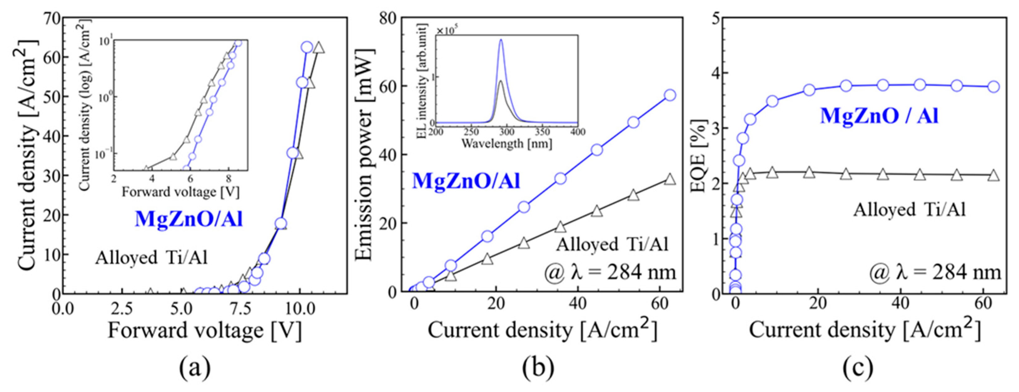
Figure 5(a) shows the absorption coefficient spectrum of only the n-type Al0.6Ga0.4N template and MgZnO (50 nm) on the n-type Al0.6Ga0.4N template. The absorption coefficients of both increased near 4.8 eV. The absorption coefficient of MgZnO on the n-type Al0.6Ga0.4N template increased near 4.0 eV. The band gap of wz-MgZnO is reported to be approximately 3.34–4.0 eV, which depends on the Mg composition [58]. The UV light absorption near 4.0 eV is attributed to wz-MgZnO. Figure 5(b) shows the thickness dependence of the transmittance of MgZnO based on the calculation from its absorption coefficient α = 1.6×105 cm−1 at the emission wavelength of 284 nm in the fabricated TJ LED. The transmittance of the MgZnO at a thickness of 50 nm is indicated as approximately 40%. We estimate a transmittance of more than 80% by reducing the MgZnO thickness to less than 10 nm for enhancing the output power of AlGaN LEDs. The TJ LED structure can be optimized by utilizing optical cavity effects toward the improvement of LEE with other enhancement approaches [77,78]. The thickness of the n-type AlGaN in contact with the AlGaN TJ should be optimized in the near-future to realize a higher output power.
4. Conclusions
We realized the improvement of the high-Al-composition AlGaN TJ deep-UV LEDs by controlling the growth of n-type AlGaN and polycrystalline MgZnO/Al electrodes. Two essential factors are considered to reduce the operating voltage of AlGaN TJ LEDs by changing the growth condition: suppression of C incorporation and doping of n+-type AlGaN at a high Si concentration. The operating voltage of AlGaN TJ LED was 10.8 V at a DC operation of 63 A/cm2. Highly reflective MgZnO/Al electrodes were fabricated as anodes for AlGaN TJ LEDs to enhance the output power of the AlGaN TJ LEDs. The output power of the 57.3 mW of TJ LED using MgZnO/Al electrodes was realized at an emission wavelength of 284 nm under the DC operation of 63 A/cm2; this was 1.7 times higher than that when using a conventional Ti/Al electrode. In the near future, the output power can be further improved by lessening the thickness of the MgZnO for AlGaN TJ LEDs.
Author Contributions
K. Nagata and T. Matsubara: writing – original draft preparation, K. Nagata, Y. Saito, M. Kushimoto, S. Tomai, S, Katsumata, Y. Honda, T. Takeuchi, and H. Amano; writing-review and editing, supervision, H. Amano. All authors have read and agreed to the published version of the manuscript.
Informed Consent Statement
Not applicable.
Acknowledgments
This work was supported by the MOE Program for the implementation of the innovative infection control and digital technologies with low CO2 emission.
Conflicts of Interest
The authors declare no conflict of interest.
References
- Oguma, K.; Rattanakul, S. UV inactivation of viruses in water: its potential to mitigate current and future threats of viral infectious diseases. Jpn. J. Appl. Phys. 2021, 60, 110502. [Google Scholar] [CrossRef]
- Minamikawa, T.; Koma, T.; Suzuki, A.; Nagamatsu, K.; Yasui, T.; Yasutomo, K.; Nomaguchi, M. Inactivation of SARS-CoV-2 by deep ultraviolet light emitting diode: A review. Jpn. J. Appl. Phys. 2021, 60, 090501. [Google Scholar] [CrossRef]
- Muramoto, Y.; Kimura, M.; Kondo, A. Verification of inactivation effect of deep-ultraviolet LEDs on bacteria and viruses, and consideration of effective irradiation methods. Jpn. J. Appl. Phys. 2021, 60, 090601. [Google Scholar] [CrossRef]
- Inagaki, H.; Saito, A.; Sugiyama, H.; Okabayashi, T.; Fujimoto, S. Rapid inactivation of SARS-CoV-2 with deep-UV LED irradiation. Emerging Microbes Infect. 2020, 9, 1744. [Google Scholar] [CrossRef] [PubMed]
- Saito, Y.; Wada, S.; Nagata, K.; Makino, H.; Boyama, S.; Miwa, H.; Matsui, S.; Kataoka, K.; Narita, T.; Horibuchi, K. Efficiency improvement of AlGaN-based deep-ultraviolet light-emitting diodes and their virus inactivation application. Jpn. J. Appl. Phys. 2021, 60, 080501. [Google Scholar] [CrossRef]
- Amano, H.; Collazo, R.; Santi, C. D.; Einfeldt, S.; Funato, M.; Glaab, J.; Hagedorn, S.; Hirano, A.; Hirayama, H.; Ishii, R.; Kashima, Y.; Kawakami, Y.; Kirste, R.; Kneissl, M.; Martin, R.; Mehnke, F.; Meneghini, M.; Ougazzaden, A.; J Parbrook, P.; Rajan, S.; Reddy, P.; Römer, F.; Rusche, J.; Sarkar, B.; Scholz, F.; J Schowalter, L. Shields, P.; Sitar, Z.; Sulmoni, L.; Wang, T.; Wernicke, T.; Weyers, M.; Witzigmann, B.; Wu, Y.; Wunderer, T.; and Zhang, Y.; The 2020 UV emitter roadmap. J. Phys. D: Appl. Phys. 2020, 53, 503001. [Google Scholar] [CrossRef]
- Ichikawa, M.; Endo, S.; Sagawa, H.; Fujioka, A.; Kosugi, T.; Mukai, T.; Uomoto, M.; Shimatsu, T. High-output-power deep ultraviolet light-emitting diode assembly using direct bonding. ECS Trans. 2016, 75, 53. [Google Scholar] [CrossRef]
- Muth, J. F.; Brown, J. D.; Johnson, M. A. L.; Yu, Z.; Kolbas, R. M.; Cook, Jr J. W.; Schetzina, J. F. Absorption coefficient and refractive index of GaN, AlN and AlGaN alloys. MRS Internet J. Nitride Semicond. Res. 1999, 4S1, G5.2. [Google Scholar]
- Katsuragawa, M.; Sota, S.; Komori, M.; Anbe, C.; Takeuchi, T.; Sakai, H.; Amano, H.; Akasaki, I. Thermal ionization energy of Si and Mg in AlGaN. J. Cryst. Growth 1998, 189/190, 528. [Google Scholar] [CrossRef]
- Jeon, S. R.; Ren, Z.; Cui, G.; Su, J.; Gherasimova, M.; Han, J.; Cho, H. K.; Zhou, L. Investigation of Mg doping in high-Al content 𝑝-type Al𝑥Ga1−𝑥N. Appl. Phys. Lett. 2005, 86, 082107. [Google Scholar] [CrossRef]
- Nakarmi, M. L.; Kim, K. H.; Khizar, M.; Fan, Z. Y.; Lin, J. Y.; Jiang, H. X. Electrical and optical properties of Mg-dopedAl0.7Ga 0.3N alloys. Appl. Phys. Lett. 2005, 86, 092108. [Google Scholar] [CrossRef]
- Nakarmi, M. L.; Nepal, N.; Ugolini, C.; Altahtamouni, T. M.; Lin, J. Y.; Jiang, H. X. Correlation between optical and electrical properties of Mg-doped AlN epilayers. Appl. Phys. Lett. 2006, 89, 152120. [Google Scholar] [CrossRef]
- Szabó, Á; Son, N. T.; Janzén, E.; Gali, A. Stampfl, C.; Neugebauer, J.; Group-II acceptors in wurtzite AlN: A screened hybrid density functional study. Appl. Phys. Lett. 2010, 96, 192110. [Google Scholar] [CrossRef]
- Lyons, J. L.; Janotti, A.; Van de Walle, C. G. Shallow versus Deep Nature of Mg Acceptors in Nitride Semiconductors. Phys. Rev. Lett. 2012, 108, 156403. [Google Scholar] [CrossRef]
- Takano, T.; Mino, T.; Sakai, J.; Noguchi, N.; Tsubaki, K.; Hirayama, H. Deep-ultraviolet light-emitting diodes with external quantum efficiency higher than 20% at 275 nm achieved by improving light-extraction efficiency. Appl. Phys. Exp. 2017, 10, 03100. [Google Scholar] [CrossRef]
- Lee, S.Y.; Han, D.S.; Lee, Y.G.; Choi, K.K.; Oh, J.T.; Jeong, H.H.; Seong, T.Y.; Amano, H. Heavy Mg doping to form reliable Rh reflective ohmic contact for 278 nm deep ultraviolet AlGaN-based light-emitting diodes. ECS J. Solid State Sci. Technol. 2020, 9, 065016. [Google Scholar] [CrossRef]
- France, R.; Xu, T.; Chen, P.; Chandrasekaran, R.; Moustakas, T. Vanadium-based Ohmic contacts to n-AlGaN in the entire alloy composition. Appl. Phys. Lett. 2007, 90, 062115. [Google Scholar] [CrossRef]
- Mori, K.; Takeda, K.; Kusafuka, T.; Iwaya, M.; Takeuchi, T.; Kamiyama, S.; Akasaki, I.; Amano, H. Low-ohmic-contact-resistance V-based electrode for n-type AlGaN with high AlN molar fraction. Jpn. J. Appl. Phys. 2016, 55, 05FL03. [Google Scholar] [CrossRef]
- Nagata, N.; Senga, T.; Iwaya, M.; Takeuchi, T.; Kamiyama, S.; Akasaki. I. Reduction of contact resistance in V-based electrode for high AlN molar fraction n-type AlGaN by using thin SiNx intermediate layer. Phys. Status Solidi c 2016, 14, 1600243. [Google Scholar] [CrossRef]
- Krishnamoorthy, S.; Akyol, F.; Park, P.S.; Rajan, S. Low resistance GaN/InGaN/GaN tunnel junctions. Appl. Phys. Lett. 2013, 102, 113503. [Google Scholar] [CrossRef]
- Minamikawa, D.; Ino, M.; Kawai, S.; Takeuchi, T.; Kamiyama, S.; Iwaya, M.; Akasaki, I. GaInN-based tunnel junctions with high InN mole fractions grown by MOVPE. Phys. Status Solidi B 2014, 252, 1127. [Google Scholar] [CrossRef]
- Yonkee, B.P.; Young, E.C.; Lee, C.; Leonard, J.T.; DenBaars, S.P; Speck, J.S.; Nakamura, S. Demonstration of a III-nitride edge-emitting laser diode utilizing a GaN tunnel junction contact. Opt. Express 2016, 24, 7816. [Google Scholar] [CrossRef]
- Neugebauer, S.; Hoffmann, M.P.; Witte, H.; Bläsing, J.; Dadgar, A.; Strittmatter, A.; Niermann, T.; Narodovitch, M.; Lehmann, M. All metalorganic chemical vapor phase epitaxy of p/n-GaN tunnel junction for blue light emitting diode applications. Appl. Phys. Lett. 2017, 110, 102104. [Google Scholar] [CrossRef]
- Hwang, D.; Mughal, A.J.; Wong, M.S.; Alhassan, A.I.; Nakamura, S.; DenBaars, S.P. Micro-light-emitting diodes with III–nitride tunnel junction contacts grown by metalorganic chemical vapor deposition. Appl. Phys. Exp. 2018, 11, 012102. [Google Scholar] [CrossRef]
- Akatsuka, Y.; Iwayama, S.; Takeuchi, T.; Kamiyama, S.; Iwaya, M.; Akasaki, I. Doping profiles in low resistive GaN tunnel junctions grown by metalorganic vapor phase epitaxy. Appl. Phys. Exp. 2019, 12, 025502. [Google Scholar] [CrossRef]
- Zhang, Y.; Krishnamoorthy, Y.; Akyol, F.; Allerman, A.A.; Moseley, M.W.; Armstrong, A.M.; Rajan, S. Design and demonstration of ultra-wide bandgap AlGaN tunnel junctions. Appl. Phys. Lett. 2016, 109, 121102. [Google Scholar] [CrossRef]
- Zhang, Y.; Krishnamoorthy, S.; Akyol, F.; Bajaj, S.; Allerman, A.A.; Moseley, M.W.; Armstrong, A.M.; Rajan, S. Tunnel-injected sub-260 nm ultraviolet light emitting diodes. Appl. Phys. Lett. 2017, 110, 201102. [Google Scholar] [CrossRef]
- Zhang, Y.; Jamal-Eddine, Z.; Akyol, F.; Bajaj, S.; Johnson, J.M.; Calderon, G.; Allerman, A.A.; Moseley, M.W.; Armstrong, A.M.; Hwang, J.; Rajan, S. Tunnel-injected sub 290 nm ultra-violet light emitting diodes with 2.8% external quantum efficiency. Appl. Phys. Lett. 2018, 112, 071107. [Google Scholar] [CrossRef]
- Pandey, A.; Shin, W.J.; Gim, J.; Hovden, R.; Mi, Z. High-efficiency AlGaN/GaN/AlGaN tunnel junction ultraviolet light-emitting diodes. Photon. Res. 2020, 8, 331. [Google Scholar] [CrossRef]
- Fan Arcara, V.; Damilano, B.; Feuillet, G.; Vézian, S.; Ayadi, K.; Chenot, S.; Duboz, J.Y. Ge doped GaN and Al0.5Ga0.5N-based tunnel junctions on top of visible and UV light emitting diodes. J. Appl. Phys. 2019, 126, 224503. [Google Scholar] [CrossRef]
- Kuhn, C.; Sulmoni, L.; Guttmann, M.; Glaab, J.; Susilo, N.; Wernicke, T.; Weyers, M.; Kneissl, M. MOVPE-grown AlGaN-based tunnel heterojunctions enabling fully transparent UVC LEDs. Photon. Res. 2019, 7, B7. [Google Scholar] [CrossRef]
- Nakamura, S.; Mukai, T.; Senoh, M.; Iwasa, N. Thermal annealing effects on P-type Mg-doped GaN Films. Jpn. J. Appl. Phys. 1992, 31, L139. [Google Scholar] [CrossRef]
- Nakamura, S.; Iwasa, N. , Senoh, M.S.; Mukai, T. Hole compensation mechanism of P-type GaN Films. Jpn. J. Appl. Phys. 1992, 31, 1258. [Google Scholar] [CrossRef]
- Limpijumnong, S.; Northrup, J.E.; Van de Walle, C.G. Identification of hydrogen configurations in p-type GaN through first-principles calculations of vibrational frequencies. Phys. Rev. B 2003, 68, 075206. [Google Scholar] [CrossRef]
- Narita, T.; Yoshida, H.; Tomita, K.; Kataoka, K.; Sakurai, H.; Horita, M.; Bockowski, M.; Ikarashi, N.; Suda, J.; Kachi, T.; Tokuda, Y. Progress on and challenges of p-type formation for GaN power devices. J. Appl. Phys. 2020, 128, 090901. [Google Scholar] [CrossRef]
- Nam, K. B.; Nakarmi, M. L.; Lin, J. Y.; Jiang, H. X. Photoluminescence studies of Si-doped AlN epilayers. Appl. Phys. Lett. 2005, 86, 222108. [Google Scholar] [CrossRef]
- Nepal, N.; Nakarmi, M. L.; Lin, J. Y.; Jiang, H. X. Photoluminescence studies of impurity transitions in AlGaN alloys. Appl. Phys. Lett. 2006, 89, 092107. [Google Scholar] [CrossRef]
- Chichibu, S. F.; Miyake, H.; Ishikawa, Y.; Tashiro, M.; Ohtomo, T.; Furusawa, K.; Hazu, K.; Hiramatsu, K.; Uedono, A. The origins and properties of intrinsic nonradiative recombination centers in wide bandgap GaN and AlGaN. J. Appl. Phys. 2013, 113, 213506. [Google Scholar] [CrossRef]
- Bryan, I.; Bryan, Z.; Washiyama, S.; Reddy, P.; Gaddy, B.; Sarkar, B.; Breckenridge, M. H.; Guo, Q.; Bobea, M.; Tweedie, J.; Mita, S.; Irving, D.; Collazo, R.; Sitar, Z. The role of transient surface morphology on composition control in AlGaN layers and wells. Appl. Phys. Lett. 2018, 112, 062102. [Google Scholar] [CrossRef]
- Nagata, K.; Makino, H.; Yamamoto, T.; Kataoka, K.; Narita, T.; Saito, Y. Low resistivity of highly Si-doped n-type Al0.62Ga0.38N layer by suppressing self-compensation. Appl. Phys. Exp. 2020, 13, 025504. [Google Scholar] [CrossRef]
- Kataoka, K.; Narita, T.; Nagata, K.; Makino, H.; Saito, Y. Electronic degeneracy conduction in highly Si-doped Al0.6Ga0.4N layers based on the carrier compensation effect. Appl. Phys. Lett. 2020, 117, 262103. [Google Scholar] [CrossRef]
- Piao, G.; Ikenaga, K.; Yano, Y.; Tokunaga, H.; Mishima, A.; Ban, Y.; Tabuchi, T.; Matsumoto, K. Study of carbon concentration in GaN grown by metalorganic chemical vapor deposition. J. Cryst. Growth 2016, 456, 137. [Google Scholar] [CrossRef]
- Sawada, N.; Narita, T.; Kanechika, M.; Uesugi, T.; Kachi, T.; Horita, M.; Kimoto, T.; Suda, J. Sources of carrier compensation in metalorganic vapor phase epitaxy-grown homoepitaxial n-type GaN layers with various doping concentrations. Appl. Phys. Exp. 2018, 11, 041001. [Google Scholar] [CrossRef]
- Kanegae, K.; Fujikura, H.; Otoki, Y.; Konno, T.; Yoshida, T.; Horita, M.; Kimoto, T.; Suda, J. Deep-level transient spectroscopy studies of electron and hole traps in n-type GaN homoepitaxial layers grown by quartz-free hydride-vapor-phase epitaxy. Appl. Phys. Lett. 2019, 115, 012103. [Google Scholar] [CrossRef]
- Narita, T.; Tomita, K.; Kataoka, K.; Tokuda, Y.; Kogiso, T.; Yoshida, H.; Ikarashi, N.; Iwata, K.; Nagao, M.; Sawada, N.; Horita, M.; Suda, J.; Kachi, T. Overview of carrier compensation in GaN layers grown by MOVPE: toward the application of vertical power devices. Jpn. J. Appl. Phys. 2020, 59, SA0804. [Google Scholar] [CrossRef]
- Lyons, J.L.; Janotti, A.; Van de Walle, C.G. Effects of carbon on the electrical and optical properties of InN, GaN, and AlN. Phys. Rev. Lett. 2014, 89, 035204. [Google Scholar] [CrossRef]
- Nagasawa, Y.; Hirano, A. A review of AlGaN-based deep-ultraviolet light-emitting diodes on sapphire. Appl. Sci. 2018, 8, 1264. [Google Scholar] [CrossRef]
- Ichikawa, M.; Fujioka, A.; Kosugi, T.; Endo, S.; Sagawa, H.; Tamaki, H.; Mukai, T.; Uomoto, M.; Shimatsu, T. High-output-power deep ultraviolet light-emitting diode assembly using direct bonding. Appl. Phys. Exp. 2016, 9, 072101. [Google Scholar] [CrossRef]
- Zhou, S.; Liu, X.; Gao, Y.; Liu, Y.; Liu, M.; Liu, Z.; Gui, C.; Liu, S. Numerical and experimental investigation of GaN-based flip-chip light-emitting diodes with highly reflective Ag/TiW and ITO/DBR Ohmic contacts. Opt. Exp. 2017, 25, 26615. [Google Scholar] [CrossRef]
- Zhou, S.; Zheng, C.; Lv, J.; Gao, Y.; Wang, R.; Liu, S. GaN-based flip-chip LEDs with highly reflective ITO/DBR p-type and via hole-based n-type contacts for enhanced current spreading and light extraction. Opt. Laser Technol. 2017, 92, 95. [Google Scholar] [CrossRef]
- Mizuhashi, M. Electrical properties of vacuum-deposited indium oxide and indium tin oxide films. Thin Solid Films, 1980, 70, 91. [Google Scholar] [CrossRef]
- Liu, J.; Wu, D.; Zeng, S. Influence of temperature and layers on the characterization of ITO films. J. Mater. Process Technol. 2009, 209, 3943. [Google Scholar] [CrossRef]
- Singh, A.; Chaudhary, S.; Pandya, D.K. High conductivity indium doped ZnO films by metal target reactive co-sputtering. Acta Materialia 2016, 111, 1. [Google Scholar] [CrossRef]
- Cao, Y.; Miao, L.; Tanemura, S.; Tanemura, M.; Kuno, Y.; Hayashi, Y.; Mori, Y. Optical properties of indium-doped ZnO films. Jpn. J. Appl. Phys. 2006, 45, 1623. [Google Scholar] [CrossRef]
- Kumar, P.M.R.; Kartha, C.S.; Vijayakumar, K.P.; Abe, T.; Kashiwaba, Y.; Singh, F.; Avasthi, D.K. On the properties of indium doped ZnO thin films. Semicond. Sci. Technol. 2005, 20, 120. [Google Scholar] [CrossRef]
- Rahmane, S.; Djouadi, M.A.; Aida, M.S.; Barreau, N.; Abdallah, B.; Hadj Zoubir, N. Power and pressure effects upon magnetron sputtered aluminum doped ZnO films properties. Thin Solid Films 2010, 519, 5. [Google Scholar] [CrossRef]
- Jiménez-González, A.E.; Urueta, J.A.S.; Suárez-Parra, R. Optical and electrical characteristics of aluminum-doped ZnO thin films prepared by solgel technique. J. Cryst. Growth 1998, 192, 430. [Google Scholar] [CrossRef]
- Minami, T.; Miyata, T.; Yamamoto, T.; Toda, H. Origin of electrical property distribution on the surface of ZnO:Al films prepared by magnetron sputtering. J. Vac. Sci. Technol. A 2000, 18, 1584. [Google Scholar] [CrossRef]
- Choi, B.H.; Im, H.B.; Song, J.S.; Yoon, K.H. Optical and electrical properties of Ga2O3-doped ZnO films prepared by r.f. sputtering. Thin Solid Films 1990, 193-194, 712. [Google Scholar] [CrossRef]
- Song, P.K.; Watanabe, M.; Kon, M.; Mitsui, A.; Shigesato, Y. Electrical and optical properties of gallium-doped zinc oxide films deposited by dc magnetron sputtering. Thin Solid Films 2002, 411, 82. [Google Scholar] [CrossRef]
- Wang, X.; Saito, K.; Tanaka, T.; Nishio, M.; Nagaoka, T.; Arita, M.; Guo, Q. Energy band bowing parameter in MgZnO alloys. Appl. Phys. Lett. 2015, 107, 022111. [Google Scholar] [CrossRef]
- Wang, X.; Saito, K.; Tanaka, T.; Nishio, M.; Guo, Q. Lower temperature growth of single phase MgZnO films in all Mg content range. J. Alloys Compd. 2015, 627, 383. [Google Scholar] [CrossRef]
- Kushimoto, M.; Sakai, T.; Ueoka, Y.; Tomai, S.; Katsumata, S.; Deki, M.; Honda, Y.; Amano, H. Effect of annealing on the electrical and optical properties of MgZnO films deposited by radio frequency magnetron sputtering. Phys. Status Solidi A 2020, 217, 1900955. [Google Scholar] [CrossRef]
- Borysiewicz, M.A.; Wzorek, M.; Gołaszewska, K.; Kruszka, R.; Pągowska, K.D.; Kamińska, E. Nanocrystalline sputter-deposited ZnMgO:Al transparent p-type electrode in GaN-based 385 nm UV LED for significant emission enhancement. Materials Science and Engineering: B 2015, 200, 93. [Google Scholar] [CrossRef]
- Borysiewicz, M.A. ZnO as a functional material, a review. Crystals 2019, 9, 505. [Google Scholar] [CrossRef]
- Imura, M.; Nakano, K.; Fujimoto, N.; Okada, N.; Balakrishnan, K.; Iwaya, M.; Kamiyama, S.; Amano, H.; Akasaki, I.; Noro, T.; Takagi, T.; Bandoh, A. Dislocations in AlN Epilayers Grown on Sapphire Substrate by High-Temperature Metal-Organic Vapor Phase Epitaxy. Jpn. J. Appl. Phys. 2007, 46, 1458. [Google Scholar] [CrossRef]
- Nagata, K.; Makino, H.; Yamamoto, T.; Saito, Y.; Miki, H. Origin of optical absorption in AlN with air voids. Jpn. J. Appl. Phys. 2019, 58, SCCC29. [Google Scholar] [CrossRef]
- Kuwano, Y.; Kaga, M.; Morita, T.; Yamashita, K.; Yagi, K.; Iwaya, M.; Takeuchi, T.; Kamiyama, S.; Akasaki, I. Lateral hydrogen diffusion at p-GaN layers in nitride-based light emitting diodes with tunnel junctions. Jpn. J. Appl. Phys. 2013, 52, 08JK12. [Google Scholar] [CrossRef]
- Alhassan, A. I.; Young, E. C.; Alyamani, A. Y.; Albadri, A.; Nakamura, S.; DenBaars, S. P.; Speck, J. S. Reduced-droop green III–nitride light-emitting diodes utilizing GaN tunnel junction. Appl. Phys. Exp. 2018, 11, 042101. [Google Scholar] [CrossRef]
- Narita, T.; Tomita, K.; Yamada, S.; Kachi, T. Quantitative investigation of the lateral diffusion of hydrogen in p-type GaN layers having NPN structures. Appl. Phys. Exp. 2019, 12, 011006. [Google Scholar] [CrossRef]
- Nagata, K.; Makino, H.; Miwa, H.; Matsui, S.; Boyama, S.; Saito, Y.; Kushimoto, M.; Honda, Y.; Takeuchi, T.; Amano, H. Reduction in operating voltage of AlGaN homojunction tunnel junction deep-UV light-emitting diodes by controlling impurity concentrations. Appl. Phys. Exp. 2021, 14, 084001. [Google Scholar] [CrossRef]
- Inazu, T.; Fukahori, S.; Pernot, C.; Kim, M. H.; Fujita, T.; Nagasawa, Y.; Hirano, A.; Ippommatsu, M.; Iwaya, M.; Takeuchi, T.; Kamiyama, S.; Yamaguchi, M. Honda, Y.; Amano, H.; Akasaki, I. Improvement of light extraction efficiency for AlGaN-based deep ultraviolet light-emitting diodes. Jpn. J. Appl. Phys. 2011, 50, 122101. [Google Scholar] [CrossRef]
- Sung, Y. J.; Kim, M.; Kim, H.; Choi, S.; Kim, Y. H.; Jung, M.; Choi, R.; Moon, Y.; Oh, J.; Jeong, H.; Yeom, G. Y. Light extraction enhancement of AlGaN-based vertical type deep-ultraviolet light-emitting-diodes by using highly reflective ITO/Al electrode and surface roughening. Opt. Exp. 2019, 27, 29930. [Google Scholar] [CrossRef] [PubMed]
- Nagata, K.; Anada, S.; Saito, Y.; Kushimoto, M.; Honda, Y.; Takeuchi, T.; Yamamoto, K.; Hirayama, T.; Amano, H. Visualization of depletion layer in AlGaN homojunction p–n junction. Appl. Phys. Exp. 2022, 15, 036504. [Google Scholar] [CrossRef]
- Nagata, K.; Anada, S.; Miwa, H.; Matsui, S.; Boyama, S.; Saito, Y.; Kushimoto, M.; Honda, Y.; Takeuchi, T.; Amano, H. Structural design optimization of 279 nm wavelength AlGaN homojunction tunnel junction deep-UV light-emitting diode. Appl. Phys. Exp. 2022, 15, 044003. [Google Scholar] [CrossRef]
- Matsubara, T.; Nagata, K.; Kushimoto, M.; Tomai, S.; Katsumata, S.; Honda, Y.; Amano, H. Sputtered polycrystalline MgZnO/Al reflective electrodes for enhanced light emission in AlGaN-based homojunction tunnel junction DUV-LED. Appl. Phys. Exp. 2022, 15, 044001. [Google Scholar] [CrossRef]
- Shen Y., C.; Wierer, J. J.; Krames, M. R.; Ludowise, M. J.; Misra, M. S.; Ahmed, F. Kim, A. Y.; Mueller, G. O.; Bhat, J. C.; Stockman, S. A.; Martin, P. S. Optical cavity effects in InGaN/GaN quantum-well-heterostructure flip-chip light-emitting diodes. Appl. Phys. Lett. 2003, 82, 2221. [Google Scholar] [CrossRef]
- Matsukura, Y.; Inazu, T.; Pernot, C.; Shibata, N.; Kushimoto, M.; Deki, M.; Honda, Y.; Amano, H. Improving light output power of AlGaN-based deep-ultraviolet light-emitting diodes by optimizing the optical thickness of p-layers. Appl. Phys. Exp. 2021, 14, 084004. [Google Scholar] [CrossRef]
Figure 1.
Deep-UV LED structures for (a) PN junction and (b) TJ devices.
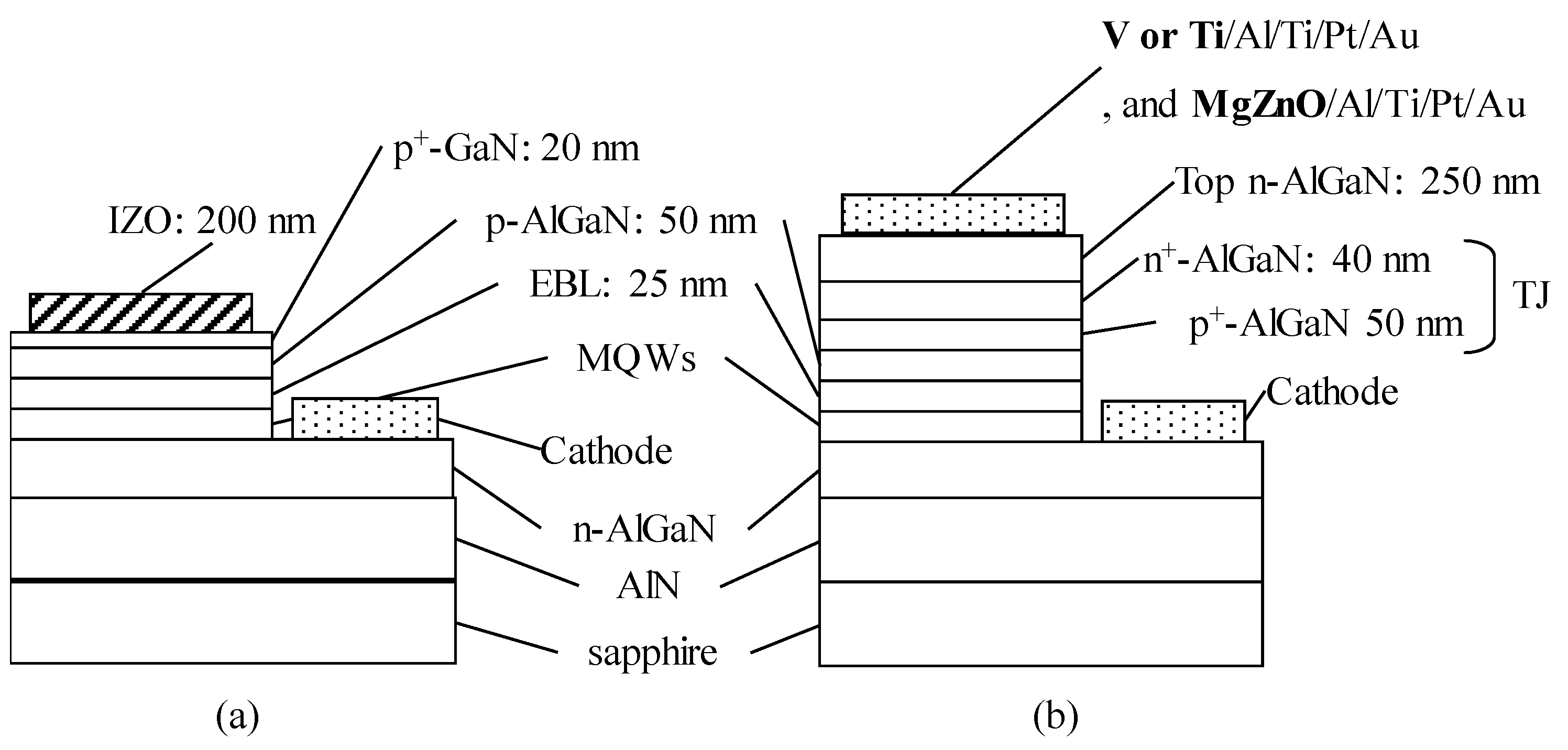
Figure 2.
Forward voltage–current density characteristics measured by DC operation at room temperature for samples PN#1, TJ#1, TJ#2, TJ#3, and TJ#4. Copyright 2021 The Japan Society of Applied Physics. [68].
Figure 2.
Forward voltage–current density characteristics measured by DC operation at room temperature for samples PN#1, TJ#1, TJ#2, TJ#3, and TJ#4. Copyright 2021 The Japan Society of Applied Physics. [68].
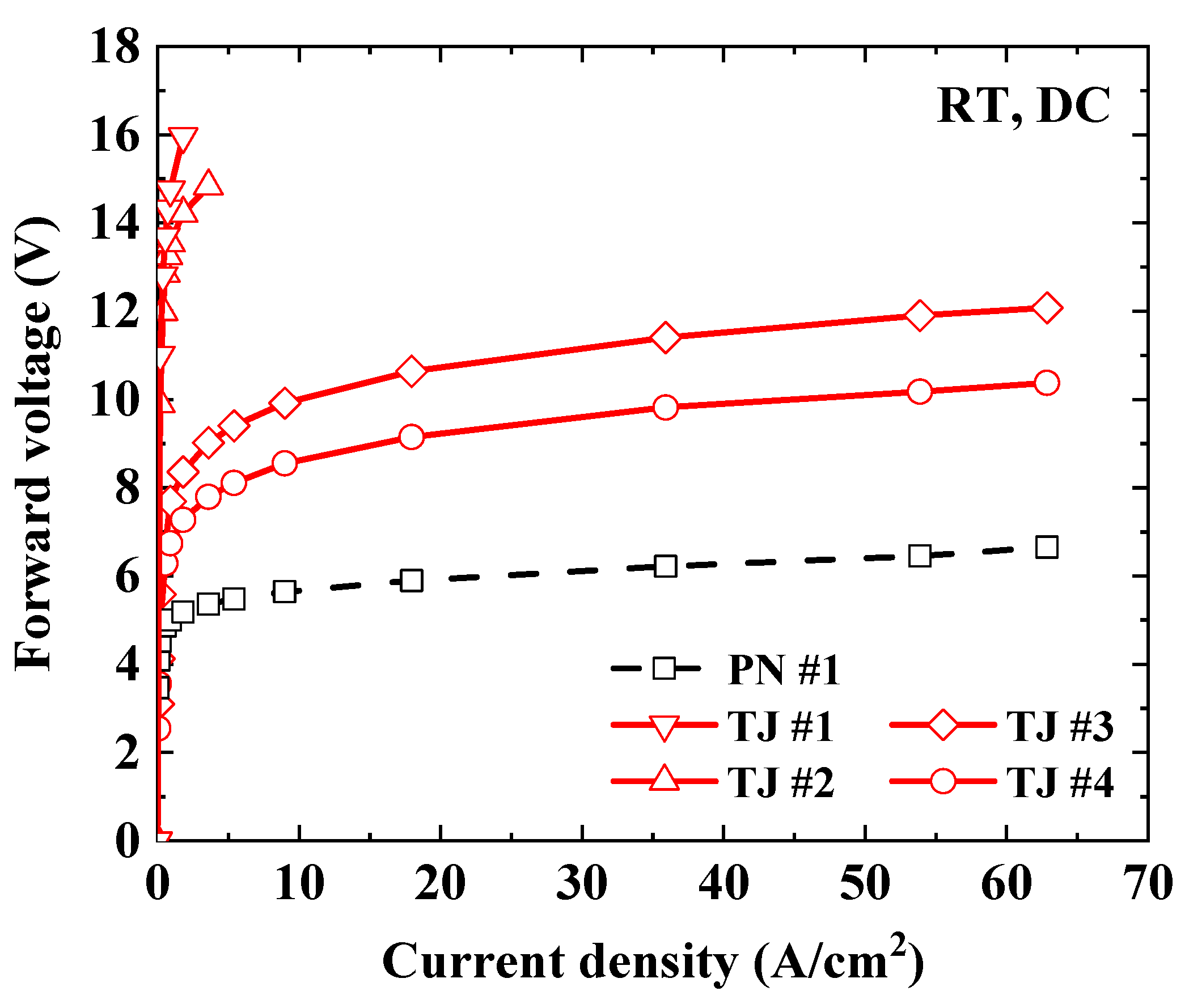
Figure 5.
Comparison of the absorption coefficient spectra of the n-type Al0.6Ga0.4N template and MgZnO deposited on the n-type Al0.6Ga0.4N. (b) Thickness dependence of the transmittance of MgZnO calculated from the absorption coefficient (α = 1.6 × 105 cm−1) at a photon energy of 4.3 eV. Copyright 2022 The Japan Society of Applied Physics [76].
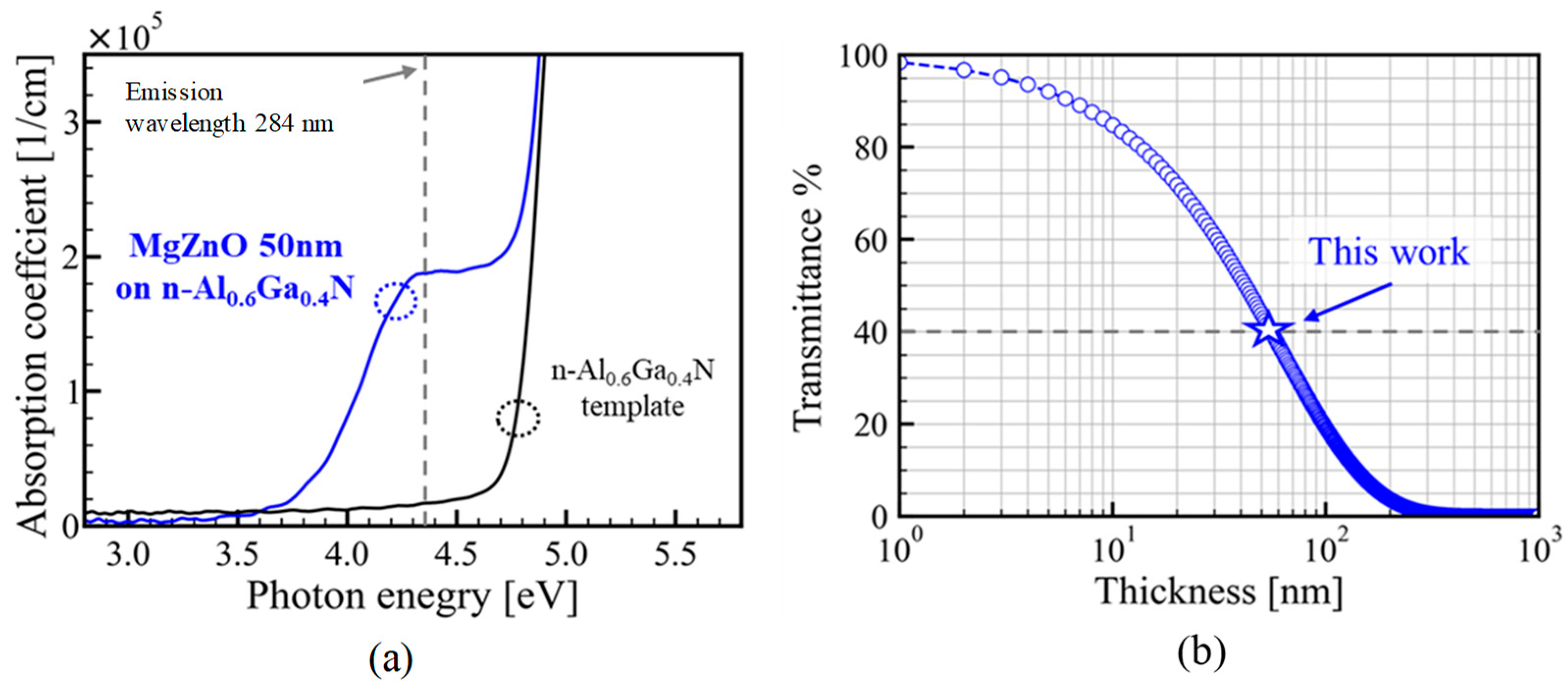
Table 2.
Summary of the evaluated parameters for all LEDs. PN and TJ indicate the PN junction and TJ LEDs, respectively. [Si] and [C] are directly measured for the samples TJ#1, TJ#3, and TJ#4, whereas [Si] and [C] in samples TJ#2 and TJ#5 (labeled by*) are estimated from the dates for TJ#1, TJ#3, and TJ#4. Copyright 2021 The Japan Society of Applied Physics. [71].
| Sample | p-AlGaN | p+-AlGaN | n+-AlGaN | ||
| Al composition | [Si] (cm−3) | [C] (cm−3) | |||
| PN | #1 | 50% | 50% | ||
| #2 | 50% | 50% | |||
| TJ | #1 | 50% | 50% | 6.3×10¹⁹ | 1.8×10¹⁸ |
| #2 | 50% | 50% | 1.3×10²⁰* | 1.8×10¹⁸* | |
| #3 | 50% | 50% | 6.3×10¹⁹ | 3.1×10¹⁷ | |
| #4 | 50% | 50% | 1.3×10²⁰ | 3.1×10¹⁷ | |
| #5 | 60% | 60% | 1.3×10²⁰* | 3.1×10¹⁷* | |
Disclaimer/Publisher’s Note: The statements, opinions and data contained in all publications are solely those of the individual author(s) and contributor(s) and not of MDPI and/or the editor(s). MDPI and/or the editor(s) disclaim responsibility for any injury to people or property resulting from any ideas, methods, instructions or products referred to in the content. |
© 2023 by the authors. Licensee MDPI, Basel, Switzerland. This article is an open access article distributed under the terms and conditions of the Creative Commons Attribution (CC BY) license (http://creativecommons.org/licenses/by/4.0/).
Copyright: This open access article is published under a Creative Commons CC BY 4.0 license, which permit the free download, distribution, and reuse, provided that the author and preprint are cited in any reuse.


