
Submitted:
20 March 2025
Posted:
21 March 2025
You are already at the latest version
Abstract
This review presents the band selective frequency technology of Electromagnetic Interference (EMI) noise spectrum spread in the DC-DC switching converter for communication devices. This technology generates notch characteristic spectrum bands with a low noise level in the received frequency band spectrum. It detects the received frequency and generates a notch band there using a switching pulse control technology. First, we introduce the conventional spread spectrum technology. By modulating the clock frequency, EMI noise is dispersed to avoid concentrating at specific frequency bands. There are both analog modulation techniques and digital modulation methods. Next, we explain the main technology of this review, the notch band generation technology. This technique involves modulating the phase or pulse width of clock to produce notch band characteristics in the EMI noise spectrum. Then we present its simulation results, theoretical analysis, and implementation results. Finally, we demonstrate a technique that tunes the notch band frequency to the received signal one automatically.
Keywords:
switching converter
; Electro-Magnetic Interference (EMI)
; noise spectrum spread
; clock pulse coding
; frequency notch characteristics
1. Introduction
Nowadays, switching power supply circuits are widely used in many electronic devices, thanks to their advantages of high efficiency, continuously variable output voltage, small size and light weight. Also, the communication circuit has been enhanced for improved performance and high-density packaging. However, since the switching power supply circuit is driven by a high-frequency clock, it generates some amounts of switching noises called EMI noises, and their reduction is very important.
In this review paper, first we explain the fundamental DC-DC switching converters employing the Pulse Width Modulation (PWM) control. They cause EMI noises at the clock and harmonics frequencies, and for their reduction, the clock modulation is often utilized by shaking its phase or frequency. This technology spreads the noise power to other frequencies, though it makes the bottom level rise-up.
Next, we review our band-selective EMI spread spectrum technique, which realizes both reduction of the spectrum line noise and generation of the low noise spectrum band like the notch filter at the receive frequency of communication devices.
2. Fundamental DC-DC Switching Converters [1,2,3,4,5,6,7,8]
There are three fundamental DC-DC switching converters: buck, boost and buck-boost types. They are composed of power and control stages, and their configurations are almost the same among three types. The power stage has a switch, an inductor, a diode, and an output capacitor. However, its construction differs among them; the differences are distinguished by their positions. The control stage of each converter is quite similar, consisting of a comparator, a D-type Flip-Flop (DFF), and a reference voltage. Their voltage conversion ratio (Vo/Vi) and polarity of Vo vary , where Vi represents the input voltage and Vo does the output voltage: 0 < Vo < Vi for the buck converter, 0 < Vi < Vo for the boost converter, and 0 < -Vo ≷ Vi for the buck-boost converter.
2.1. Buck Converter with PWM Control
Figure 1 shows the configuration of the buck converter. The red/blue broken line represents the current flow when the PWM pulse is high/low, respectively. The power stage is composed of a switch (SW), an inductor (L), a diode (Di), and an output capacitor (Co). The control stage is composed of an amplifier (AMP), a comparator (CMP), a D-type Flip-Flop (DFF), and a sawtooth generator.
In the power stage, SW is regulated by the PWM signal. In case the PWM signal is high, SW turns ON, and the input current from the power supply flows through SW to L (as shown by the red broken line in Figure 1). During this period, the input current increases, flowing into Co and RL, resulting in an increase in Vo (Figure 2) and raising the magnetic energy in L. Conversely, when the PWM level is low, SW turns OFF, and the energy stored in L causes the current to flow through Di (as indicated by the blue dotted line in Figure 2). Then, Vo decreases and the duty ratio (D) of the PWM signal increases.
In the control stage, the AMP amplifies the voltage error of Vo and the reference voltage (Vref). This amplified error voltage is then compared with the sawtooth signal (SAW) and the PWM signal is generated. The DFF receives this data synchronously with the internal clock (CK) to provide the SAW pulse so that the SAW signal is generated by the sawtooth generator. Vo varies based on D, and Vo is related to D as shown by:
Vo = D・Vi (1)
Vo is less than Vi due to 0 < D < 1.
Figure 1.
Configuration of the buck converter.
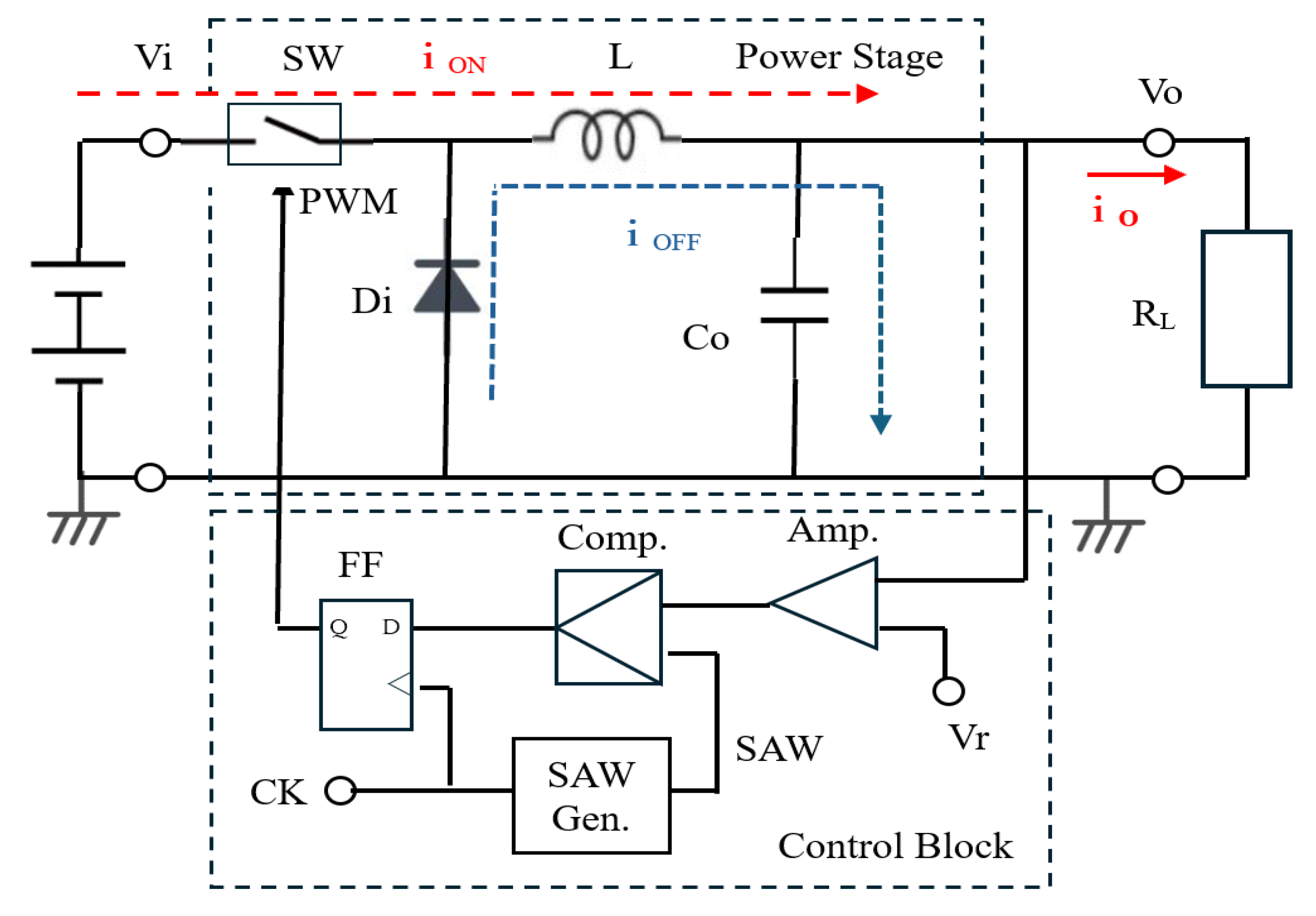
Figure 2.
Waveforms of the buck converter.

2.2. Boost Converter
Figure 3 shows the configuration of the boost converter. When SW is ON, the input current flows through L, and it does not flow to Co or RL (Figure 3), and then L charges the magnetic energy. When SW is OFF, the current to flow from L to Co and RL through Di. As a result, the current into Co is intermittently interrupted, leading to some output voltage ripple. Vo is expressed by
Vo = 1/(1ーD)・Vi (2)
Notice 1 < 1/(1-D) and Vo > Vi.
Figure 3.
Configuration of the boost converter.

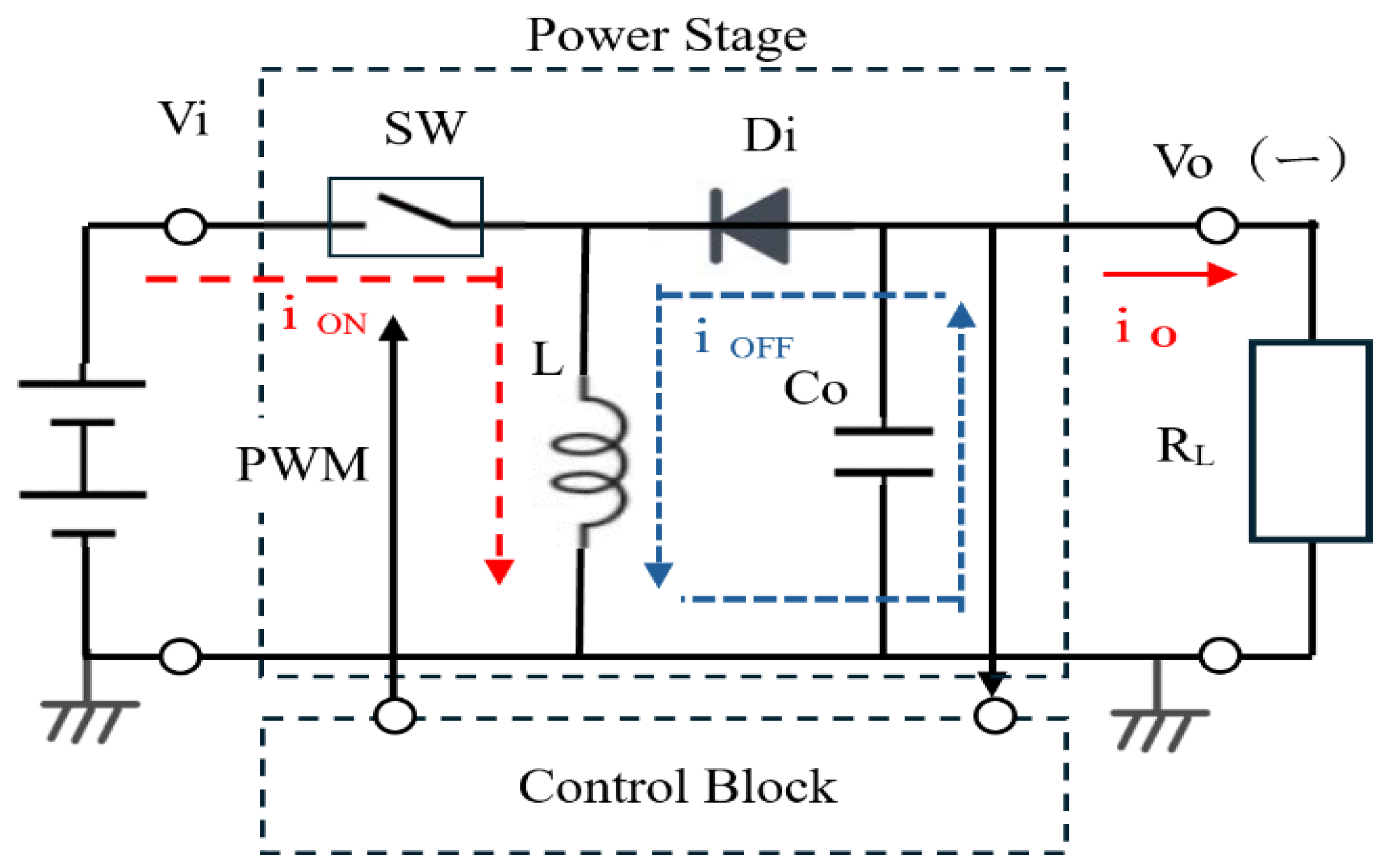
2.3. Buck-Boost Converter
The buck-boost converter produces a negative voltage output. Figure 4 illustrates its configuration, and it operates as follows:
・In case SW is ON, the input current flows through SW and L.
・In case SW is OFF, the inductor current flows into Co in a inverse direction, as shown by the blue dotted line in Figure 4. As a result, the polarity of Vo becomes negative. Vo can be expressed by Eq. (3), and the absolute value of Vo varies widely over or less than Vi.
Vo = -D/(1-D)・Vi (3)
Figure 4.
Configuration of the buck-boost converter.
3. Conventional Method of EMI Reduction with Suppressing Diffusion [9,10,11,12,13,14,15,16,17,18,19,20,21,22,23,24]
This section reviews some spread spectrum technology for EMI reduction with diffusion suppression of power supply and switching noises. Basic spread spectrum technologies for clock noise involve modification of the clock with frequency, phase and pulse width. The following will illustrate the one with the coding of the clock using both analog and digital methods.
3.1. Frequency Modulation with Analog Spread Spectrum Clock Generator
(A) Configuration and operation
It is recognized that the clock frequency or phase modulation in switching converters spreads the power spectrum of the EMI noise from the PWM signal and decreases its peak level at the clock and harmonics frequencies. Figure 5 shows the conventional clock frequency modulator and Figure 6 shows its associated signals. There, the voltage-controlled oscillator (VCO) is incorporated for the modulation of the frequency or phase of the SAW signal (Figure 6).
Figure 7a illustrates the spectrum of the PWM signal without clock modulation, whereas Figure 7b illustrates the one with modulation by two frequencies. The clock noise power spectrum is spread around the clock and harmonics frequencies. Several line spectra, indicated by the solid arrows, are discretely spread (marked by the dashed arrows); there the peak power levels are reduced.
(B) Simulation results
Figure 8 illustrates the spectrum of the PWM pulse without clock modulation. At the clock frequency of 0.5 MHz, a line spectrum reaching 3.5 V is observed, along with many harmonics. For the clock noise reduction, its modulation is utilized by shaking its phase or frequency (Figure 5). Figure 9 displays the spectrum with modulation. Since the power at the clock and harmonics frequencies spread to other bands, their peak levels become lower, though the bottom level becomes higher.
3.2. Basic Digital Frequency Modulation with LFSR
(A) Configuration and generated pseudo analog signal
Pseudo-analog noise generation using a Phase Locked Loop (PLL) clock generator for modulation is reviewed.
Figure 10 illustrates the 3-bit Linear Feedback Shift Registers (LFSRs) or M-sequence circuits. Based on G3_1(x) in Eq. (4), the outputs of the 3rd and 2nd bits are connected to the inputs of the Exclusive NOR (EX-NOR) gate, and its output is provided to the first DFF. The n-bit LFSR generates K (=2n -1) levels, where n is the order of the primitive polynomial. For n=3, K is 7 and there are two primitive polynomials G3_1(x) in Eq. (4) and G3_2(x) in Eq. (5).
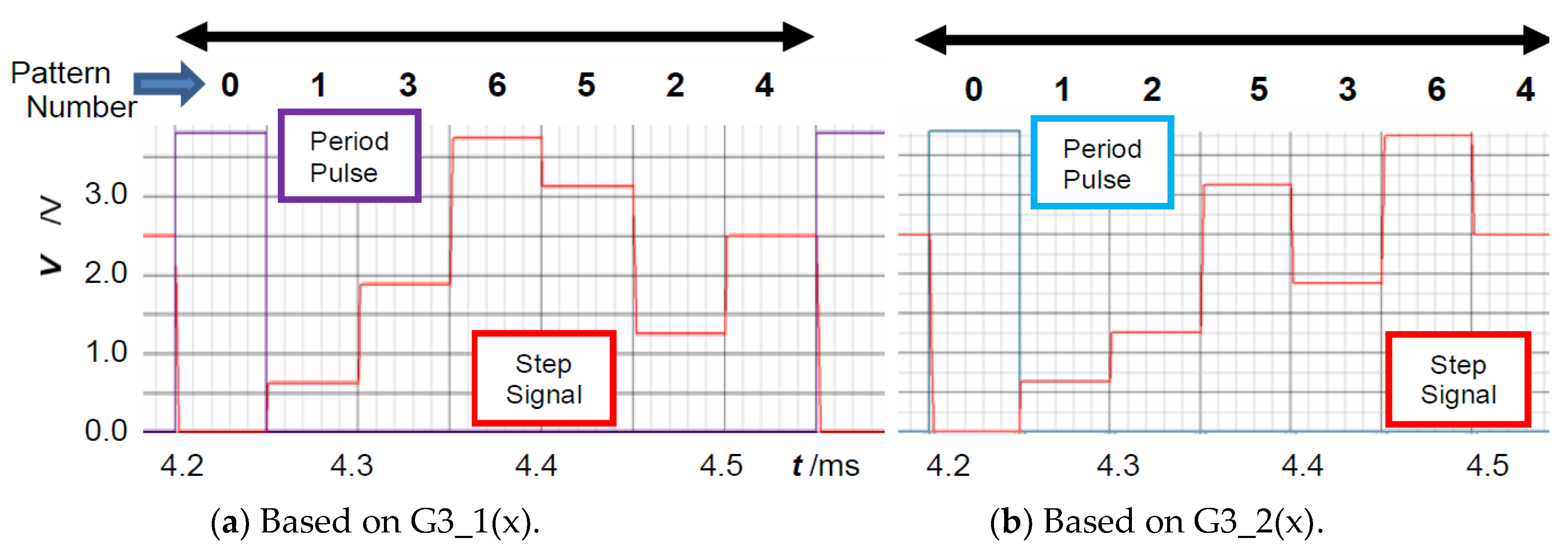
Figure 11 illustrates the analog output levels obtained from (Q3, Q2, Q1) by the LFSR in Figure 10. There are periodic patterns with 7 levels: 0-1-3-6-5-2-4 or 0-1-2-5-3-6-4. These are transformed into a smooth signal as pseudo-analog noise. This pseudo analog noise is introduced into the PLL, and then, its output is frequency-modulated (Figure 12). Also, the PLL does not lock to the input noise due to its sluggish step response characteristics (Figure 13).
G3_1(x) = x3 + x2 + 1 (4)
G3_2(x) = x3 + x + 1 (5)
Figure 10.
3-bit LFSRs for two primitive polynomials [24] @JTSS.
Figure 10.
3-bit LFSRs for two primitive polynomials [24] @JTSS.
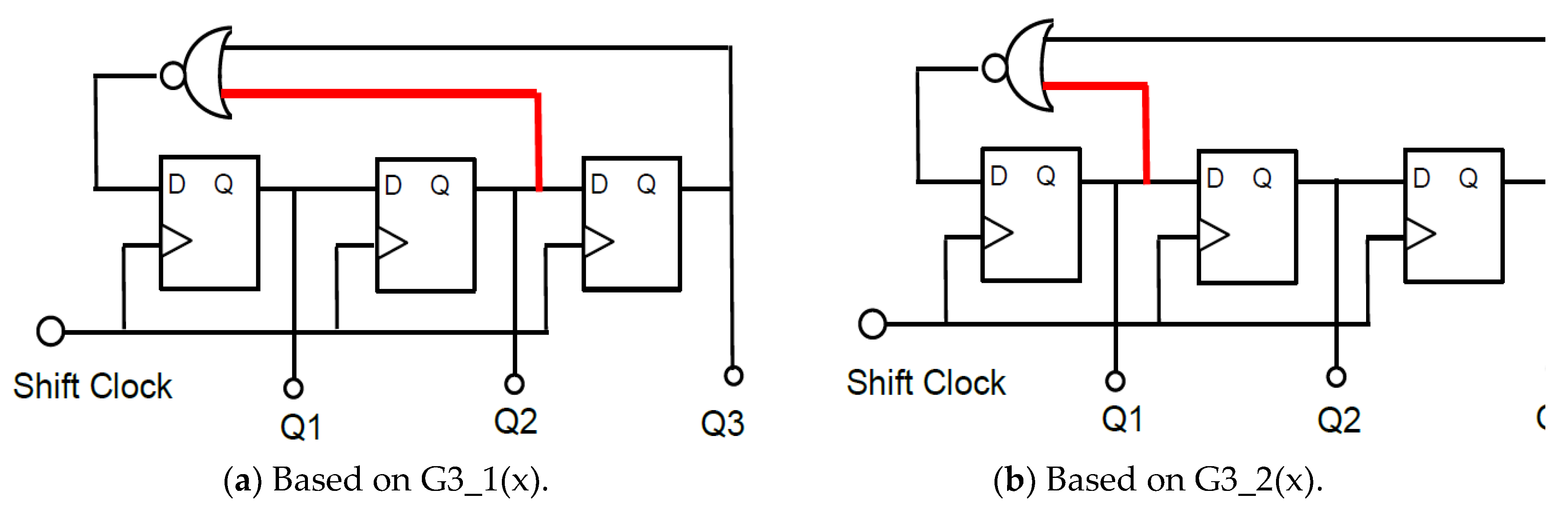
Figure 11.
Waveforms of output levels with LFSRs [24] @JTSS.
Figure 11.
Waveforms of output levels with LFSRs [24] @JTSS.
(B) Simulation of clock modulation with pseudo analog noise
The clock generator with modulation by the pseudo analog noise is illustrated in Figure 12. The generated pulse train by the LFSR in Figure 10 is converted to the analog signal by the DAC and smoothed by the LPF, and it is supplied to the PLL. Figure 13 shows its simulated characteristics of the damped vibrated signal when the input signal is changed with some steps.
Figure 12.
Configuration of the clock generator with analog modulation [24] @JTSS.
Figure 12.
Configuration of the clock generator with analog modulation [24] @JTSS.
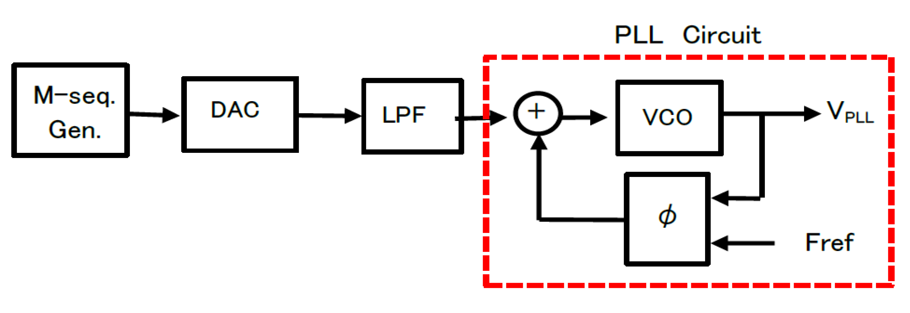
Figure 13.
Step response of the PLL [24] @JTSS.
Figure 13.
Step response of the PLL [24] @JTSS.
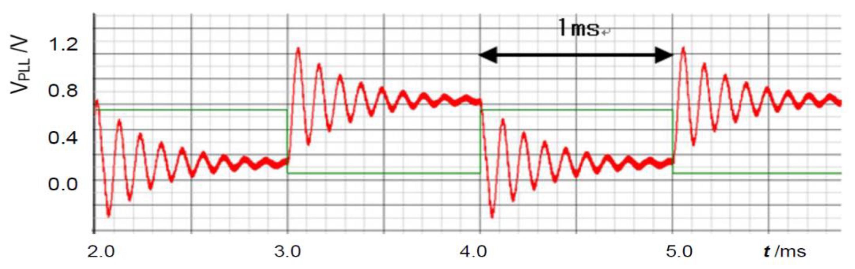
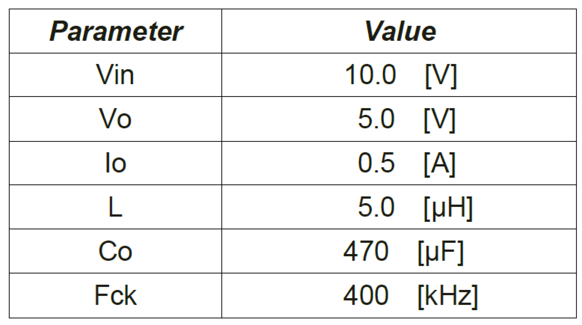
Figure 14 displays the pseudo analog noise (Vn: periodic), the VCO input signal (Vcont: non-periodic) and the output voltage ripple (⊿Vo: non-periodic) when an LFSR based on G3_1(x) is used. The clock frequency is 400 kHz, while the shift clock of the LFSR in Figure 10 is 10 kHz. Then the periodic frequency of Vn is 1.43 kHz, and ⊿Vo is about 10mVpp. Table 1 shows the simulation parameters, and SIMPLIS is used as simulator.
Figure 15 displays the simulated spectra of the PWM signal (red) and the conducted noise (green). Figure 15a displays the spectra without the pseudo-analog noise (Np), whereas Figure 15b includes the ones with Np. The peak level at the clock frequency is reduced from 3.0V to 0.55V, and that at the 3rd harmonic is from 1.0V to 0.1V, while that of the conductive noise is from 350mV to 70mV.
Figure 14.
Signals associated with PLL circuit [24] @JTSS.
Figure 14.
Signals associated with PLL circuit [24] @JTSS.
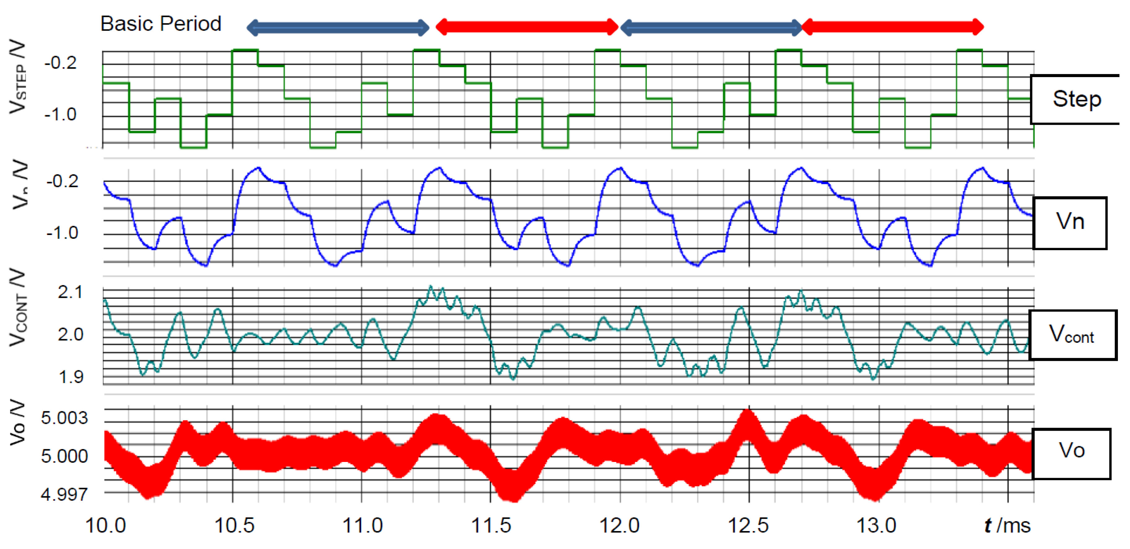
Figure 15.
Spectrum of PWM and conductive noises [24] @JTSS.
Figure 15.
Spectrum of PWM and conductive noises [24] @JTSS.
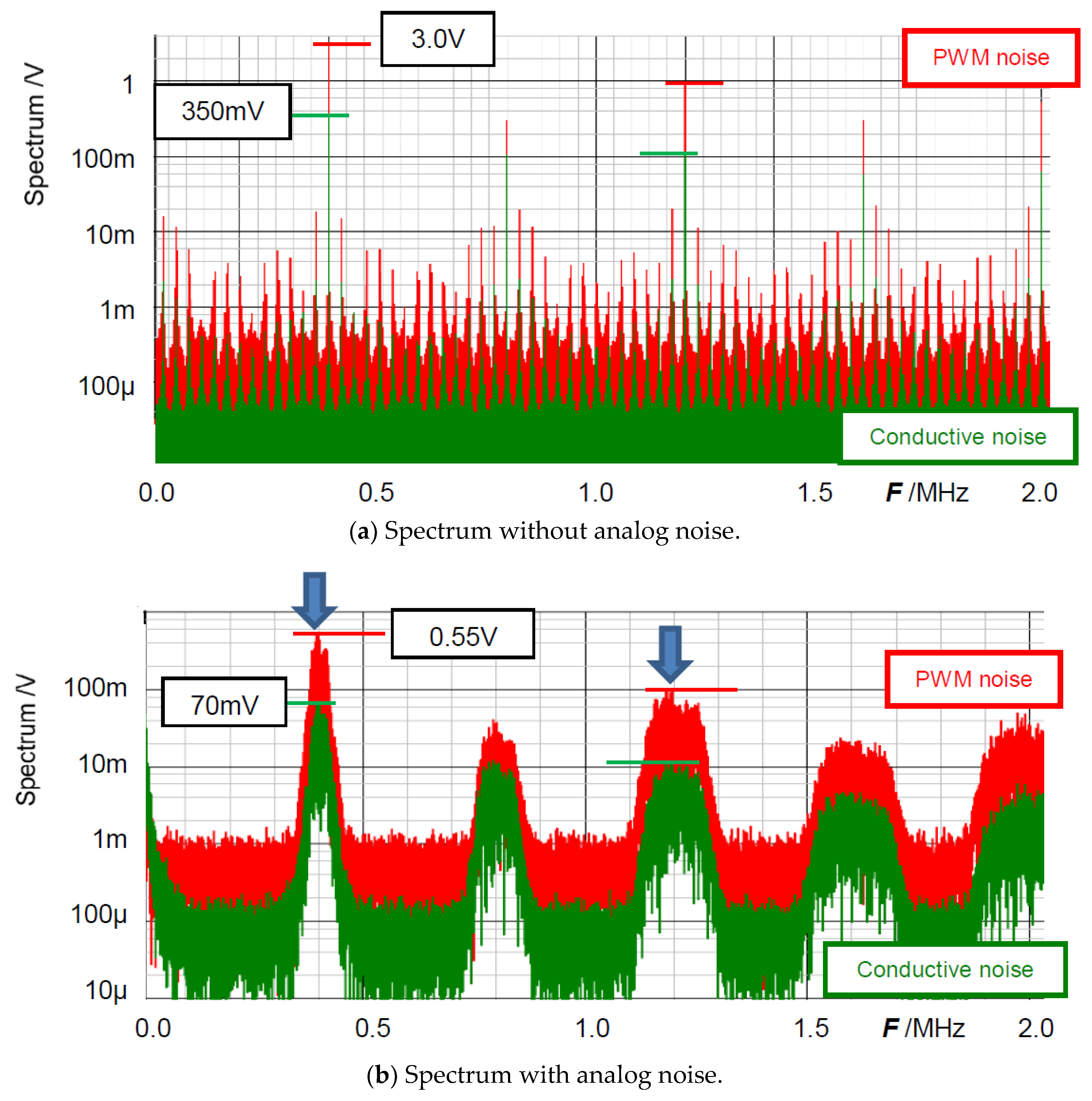

Table 1.
Simulation parameters.
3.3. Analog Noise Generators using Bit Operation
(A) Expansion of analog pattern length using bit-inverse
We explain an analog noise generator using bit-exchange for an LFSR. The longer the period of the analog noise, the lower the peak level at the specific frequency, resulting in a broader sideband spectrum. The 3-bit system produces 8 analog levels, and the number of permutations of the pattern levels is 7P7 = 5,040. Thus, a larger number of the bits increases the number of permutations. For instance, inversing some of the bits from the LFSR output produces other pattern levels.
Additional patterns from the combination of these pattern levels are included. Eqs. (6)- (13) illustrate the results of the bit-inversed level streams of Eqs. (4) (5). Usage of these streams extends the analog noise period to 8 times that of the original. The pattern length using the bit-inverse results in T1 =8・2・7=16・To, where To is the original pattern length of 7.
【Based on G3_1(x)】 : 【Based on G3_2(x)】
(B) Simulation results of pattern generator with bit-inverse
Figure 16 illustrates the simulation circuit of the LFSR (M-sequence circuit) with bit-inverse based on G3_1(x). The bit-inverse uses three EX-NOR gates, in conjunction with a 3-bit binary counter, that is triggered once within a period of the LFSR counter. In Figure 16, the binary counter increments when all bits of the LFSR counter are zero, and CK is triggered when all the outputs of the binary counter are zero. The periodic length of the 3-bit DAC input (B3, B2, B1) extends to 8 times of To (Figure 16 and Figure 17).
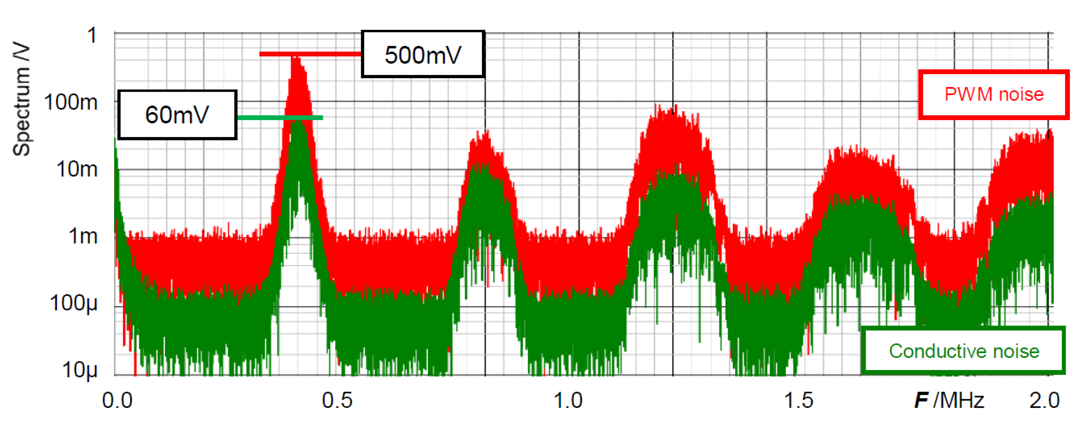
Figure 18 displays the output voltage ripple (⊿Vo) of the converter using pseudo analog noise, while Figure 19 illustrates the spectrum of the PWM signal and the conductive noise using bit-inverse. The ripple voltage is 8.5 mVpp. The peak level at the clock frequency is reduced from 550 mV to 500 mV, and the level of the conductive noise is from 70 mV to 60 mV, compared to Figure 15b.
Figure 16.
Pattern generator using bit-inverse [24] @JTSS.
Figure 16.
Pattern generator using bit-inverse [24] @JTSS.
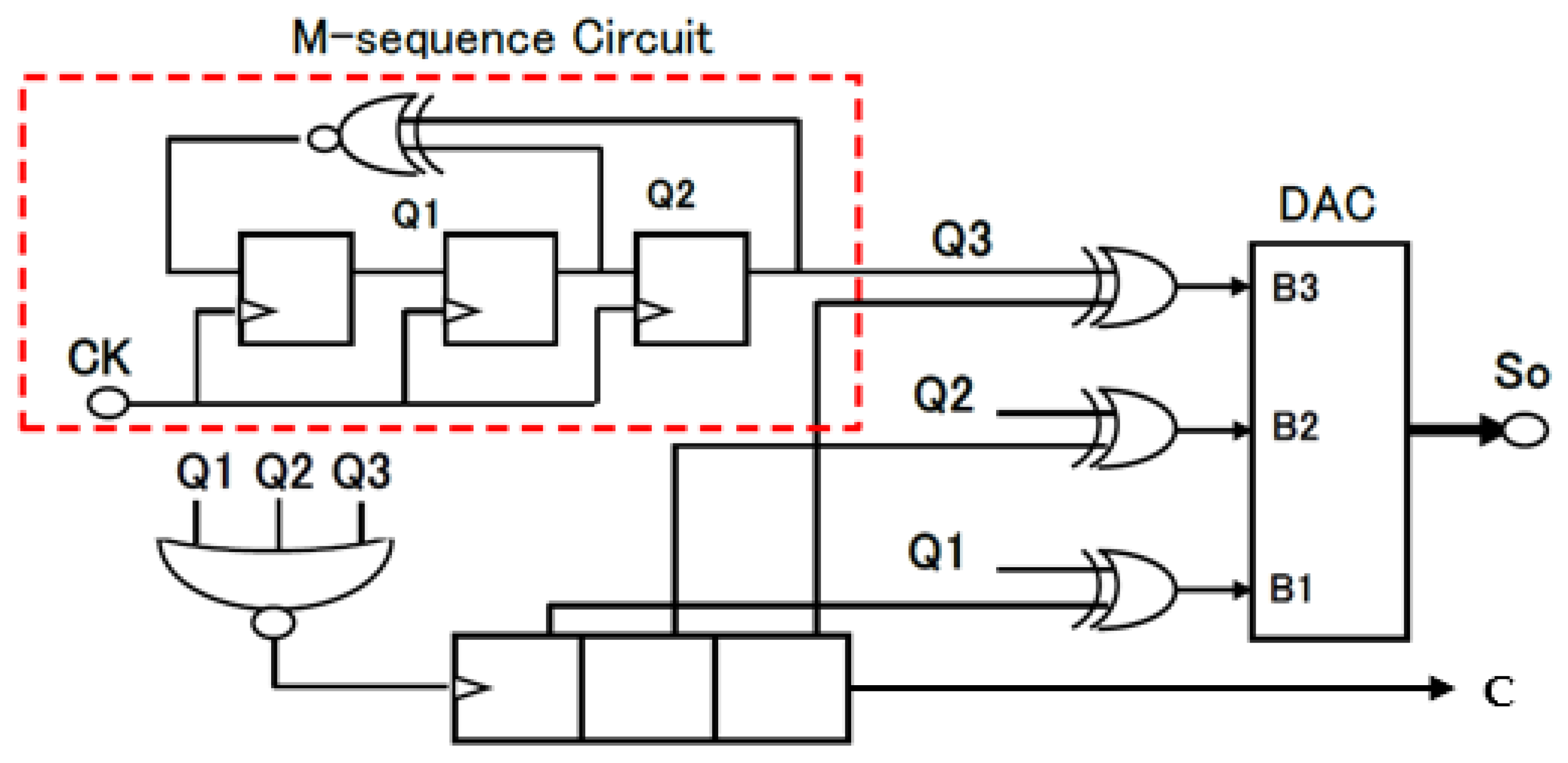
Figure 17.
Expanded pattern length using bit-inverse [24] @JTSS.
Figure 17.
Expanded pattern length using bit-inverse [24] @JTSS.
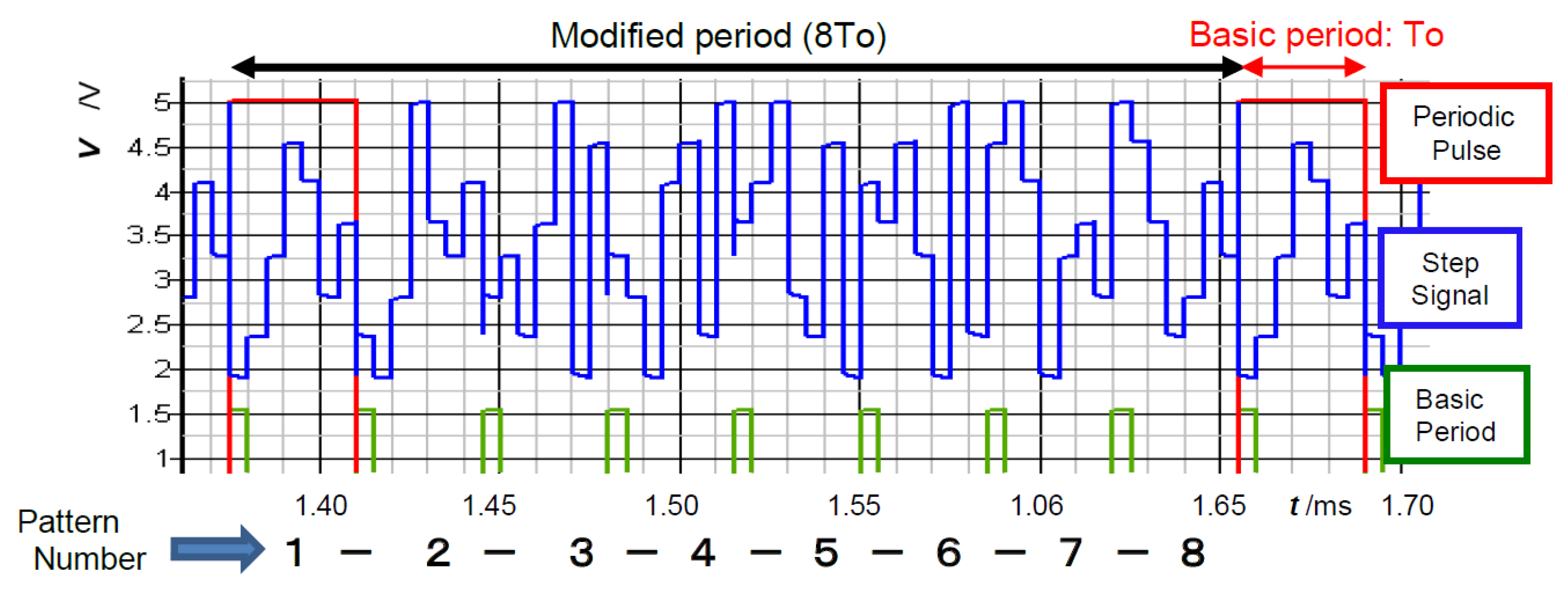
Figure 18.
Output ripple of the buck converter using bit-inverse [24] @JTSS.
Figure 18.
Output ripple of the buck converter using bit-inverse [24] @JTSS.
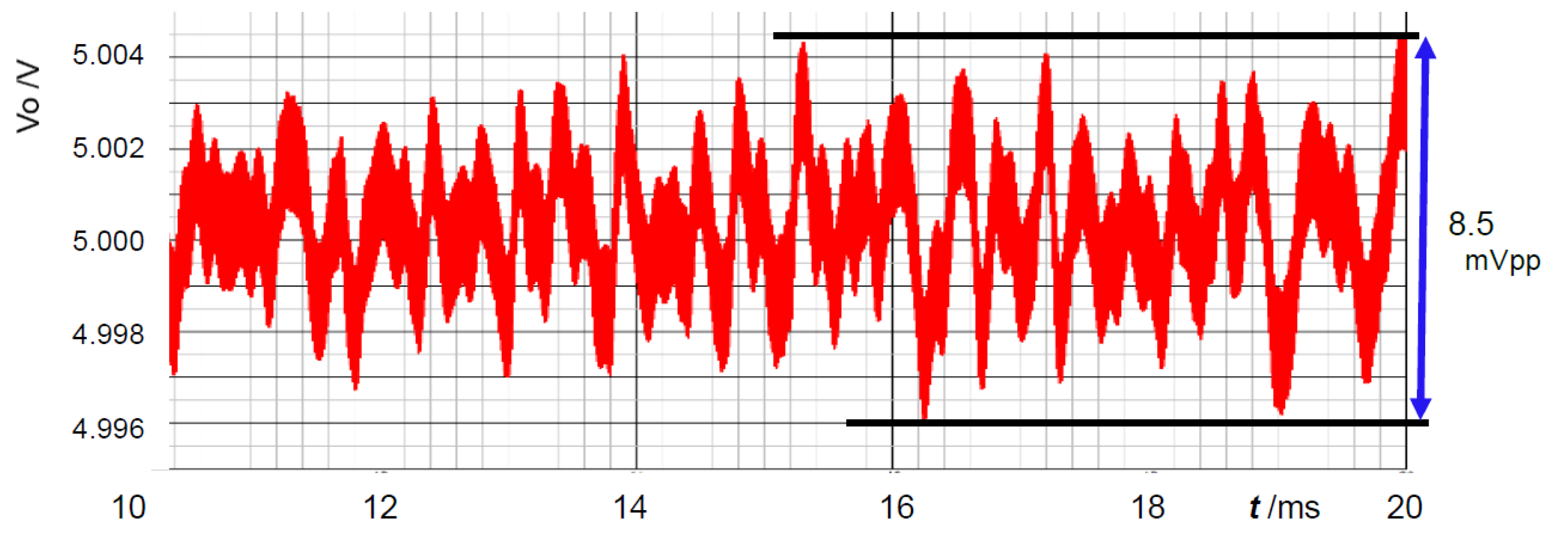
Figure 19.
Spectrum of the buck converter output using bit-inverse [24] @JTSS.
Figure 19.
Spectrum of the buck converter output using bit-inverse [24] @JTSS.
3.4. Pattern Generator Using Bit-Inverse and Bit-Exchange and Simulation Results
(A) Expansion of analog pattern length using bit-inverse and bit-exchange
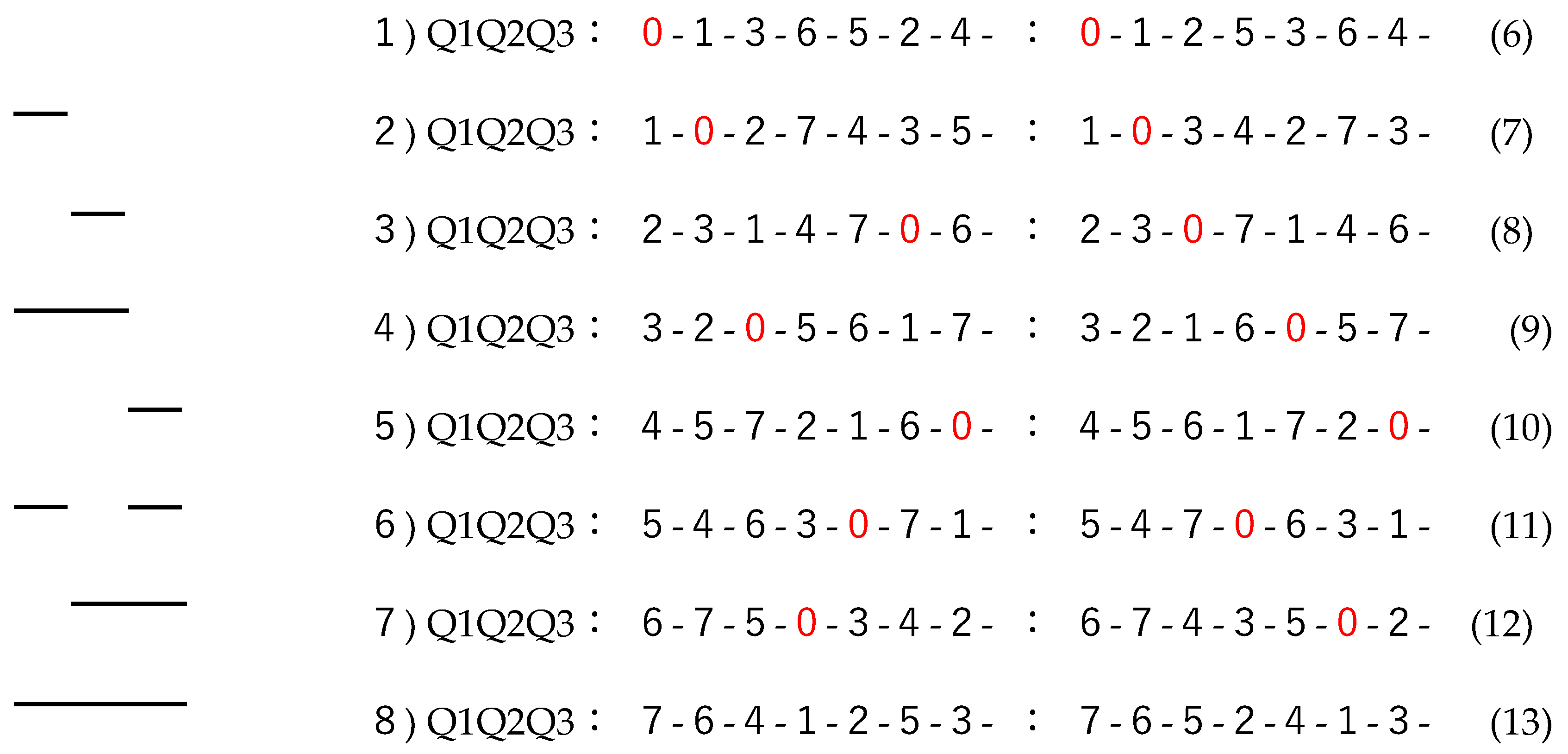
The bit-exchange technique for expansion of the analog noise period is introduced. There are no identical bit streams compared to Eqs. (6)-(13). The new pattern length becomes 6 times the one with only bit-inverse (T2 = 6・T1 =96・To).
【Based on G3_1(x)】 : 【Based on G3_2(x)】
1) Q1Q2Q3 : 0-1-3-6-5-2-4- : 0-1-2-5-3-6-4- [basic] (6)
2) Q1Q3Q2 : 0-1-5-6-3-4-2- : 0-1-3-5-2-4-6- (14)
3) Q2Q1Q3 : 0-2-3-5-6-1-4- : 0-6-2-3-5-1-4- (15)
4) Q2Q3Q1 : 0-4-5-3-6-1-2- :0-4-3-2-5-1-6- (16)
5) Q3Q1Q2 : 0-2-6-5-3-4-1- :0-6-5-3-2-4-1- (17)
6) Q3Q2Q1 : 0-4-6-3-5-2-1- : 0-4-5-2-3-6-1- (18)
(B) Simulation results of pattern generator using bit-inverse and bit-exchange
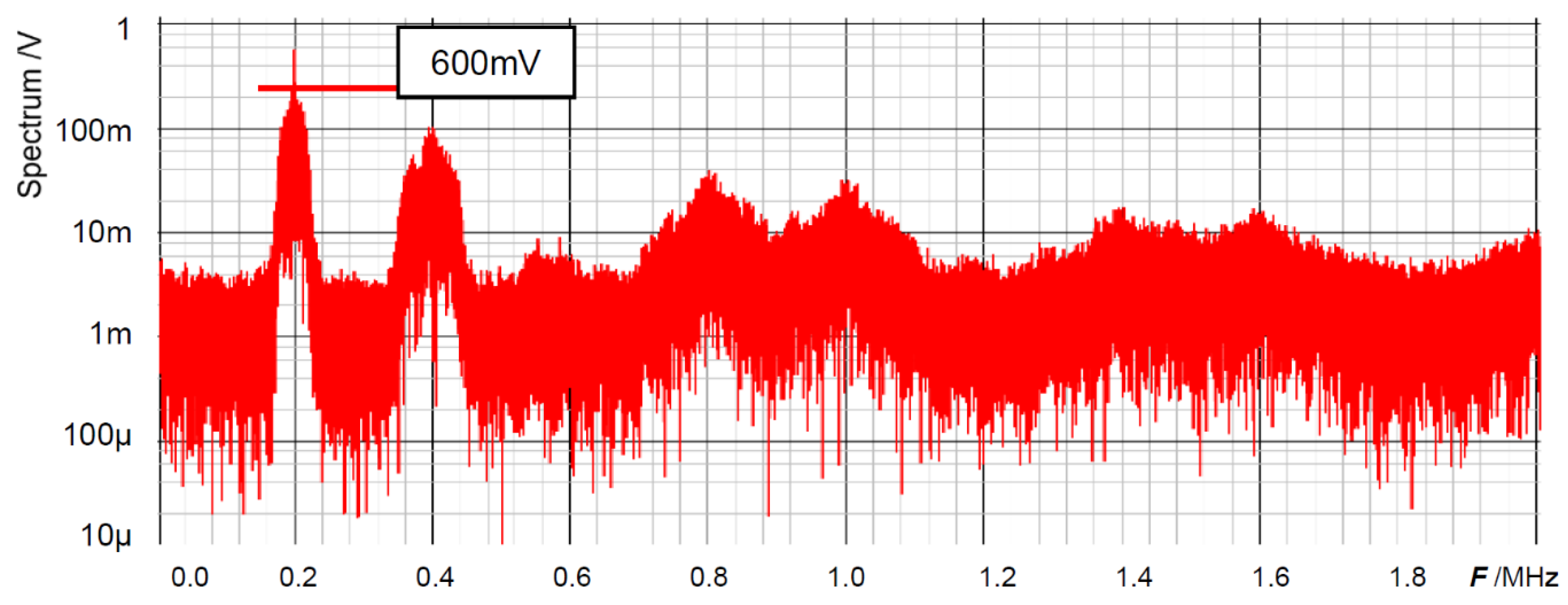
Figure 20 illustrates the configuration of the LFSR using bit-inverse and bit-exchange. The bit-inverse circuit is shown in Figure 16 and the bit-exchange circuit is composed of a multiplexer array. At the 3-bit DAC output, the number of the analog steps is 48 times of the original pattern one and Figure 21 illustrates its output of the expanded bit-pattern. Figure 22 illustrates its simulated spectra. The peak level of the PWM pulse noise is reduced from 500 mV to 400 mV (-17.5 dB), while the conductive noise remains 60 mV, compared to Figure 19.
3.5. Expansion of Number of Pseudo Analog Noise Generator Bits
(A) Expansion of number of bits
We found that it is not the number of bits for the LFSR that reduces EMI noise, but rather the ratio of the variation in pattern levels of the LFSR. There are two 4th-order primitive polynomials and the bit level series are given in Eqs. (27), (28), while the number of the pattern variations is To=24-1=15.
[4th-order] G4_1(y)=y4+y3+ (19)
G4_2(y)= y4+y +1 (20)
[Pattern] G4_1:0-1-3-7-14-13-11-6-12-9-2-5-10-4-8- (21)
G4_2:0-1-2-5-10-4-9-3-6-13-11-7-14-12-8- (22)
(B) Simulation results with 4th-order primitive polynomials
Figure 23 illustrates the output step pattern from the 4-bit LFSR and the output of the LPF following the 4-bit DAC with the bit-inversed versions of Eqs. (19) and (20). The step pattern consists of non-periodic pulses, because the condition of the initial bit patterns in the LFSR varies based on the previous ones. Figure 24 illustrates the spectrum of the PWM pulse. The peak level is 600 mV, which matches the one with 3rd-order primitive polynomials.
There is little difference in EMI reduction of the 3-bit and 4-bit LFSRs with bit-inverse operation. Therefore, only the 3-bit LFSR is sufficient, and we see that fine frequency changes in modulation are not necessary.
Figure 23.
Signals of 4-bit LFSR with bit-inverse [24] @JTSS.
Figure 23.
Signals of 4-bit LFSR with bit-inverse [24] @JTSS.
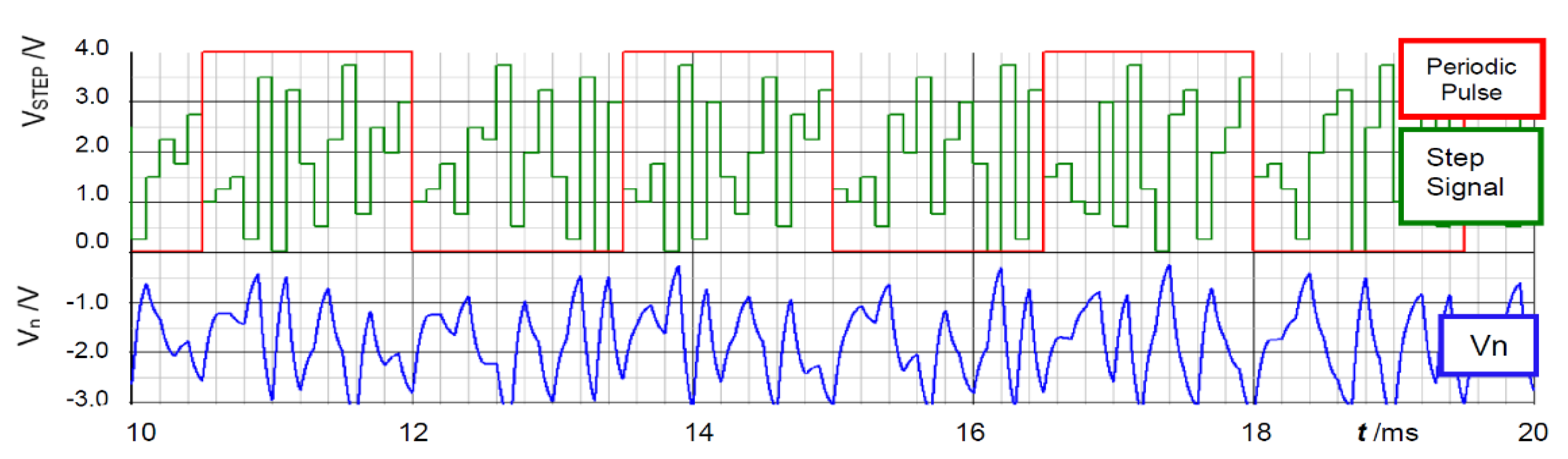
Figure 24.
Spectrum of PWM pulse using 4-bit LFSR with bit-inverse [24] @JTSS.
Figure 24.
Spectrum of PWM pulse using 4-bit LFSR with bit-inverse [24] @JTSS.
4. Notch Band Select with Pulse Coding Control [25,26,27,28]
This section reviews our EMI noise spread spectrum techniques with notch band select using pulse coding methods: Pulse Width Coding (PWC), Pulse Cycle Coding (PCC), Pulse Width and Phase Coding (PWPC). The notches appear at frequencies determined by empirical equations. We demonstrate the relationships of the notch frequencies and the coded pulses in simulation. Also, their analytical formulae are shown.
4.1. Pulse Width Coding (PWC) Control
(A) Basic pulse coding control
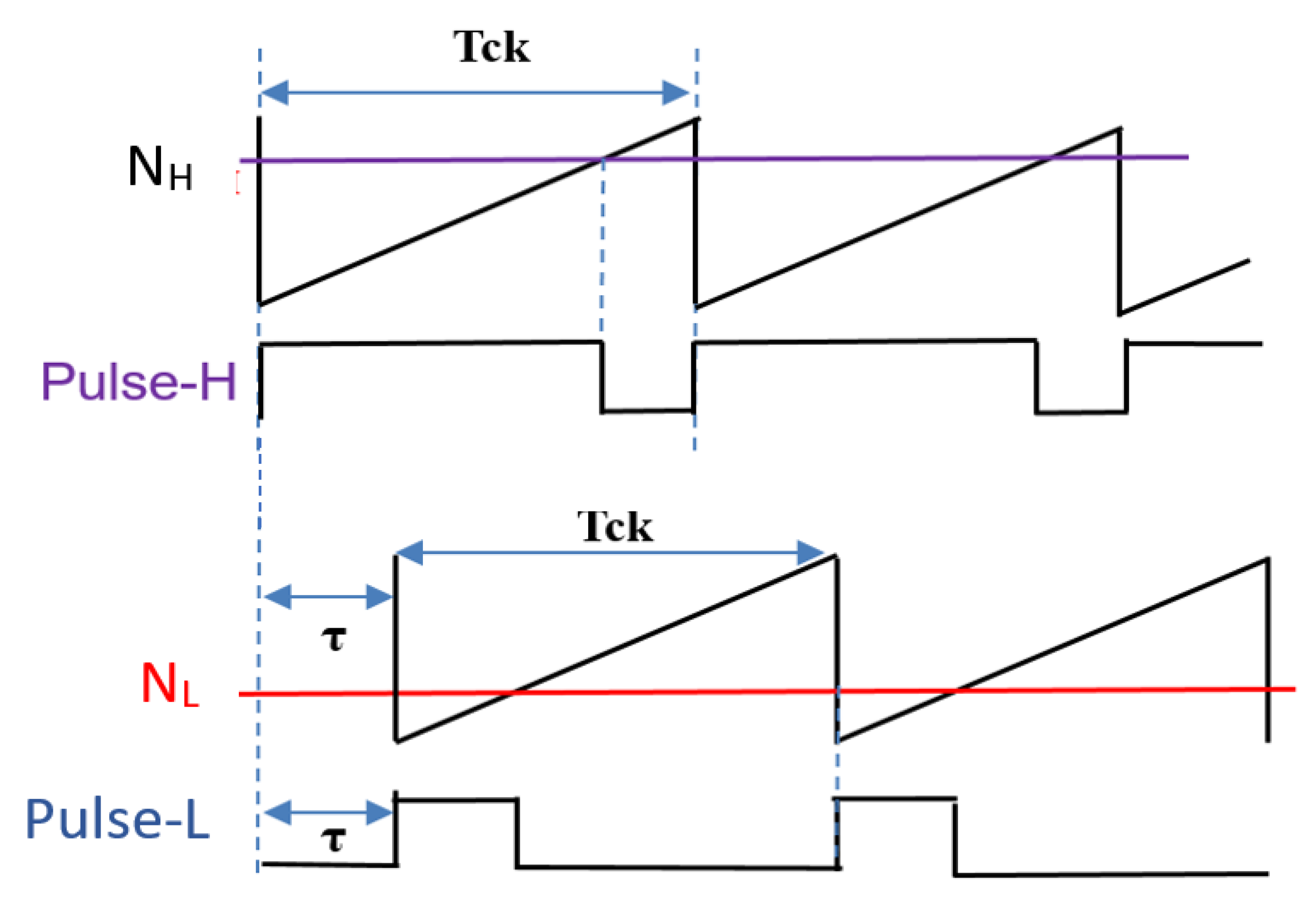
In the pulse coding control method, the switch is regulated by the Pulse Coded Drive (PCD) signal, that is selected from two coded PWM pulses (Figure 25). Pulse 1 and Pulse 2 are generated using various coding methods with parameters of pulse width, phase and their composite, and then, one is selected by SEL.
(B) Pulse Width Coding (PWC) control
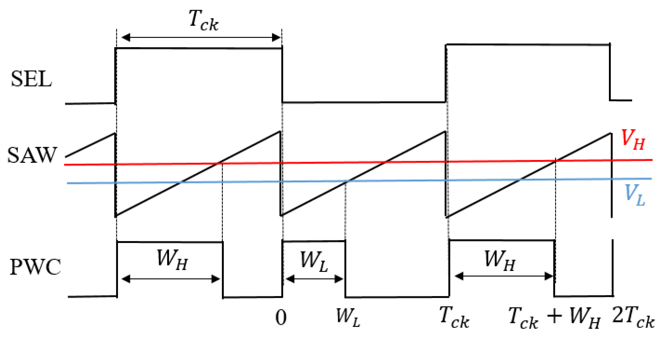
The PWC method discretely modulates the feedback pulse width. Figure 26 illustrates the PWC control circuit, and there SEL is generated from the error voltage (Verr). Figure 27 illustrates SEL, , , and PWC pulse (, ). When SEL is high, the multiplexer selects , and the comparison with SAW generates . When SEL is low, it selects , and the comparison with SAW generates . The output voltage is stably controlled by satisfying the following:
DL < Do (= Vo / Vi ) < DH (23)
Here, DL = WL / Tck and DH = WH / Tck in Figure 27.
Figure 26.
PWC control circuit.
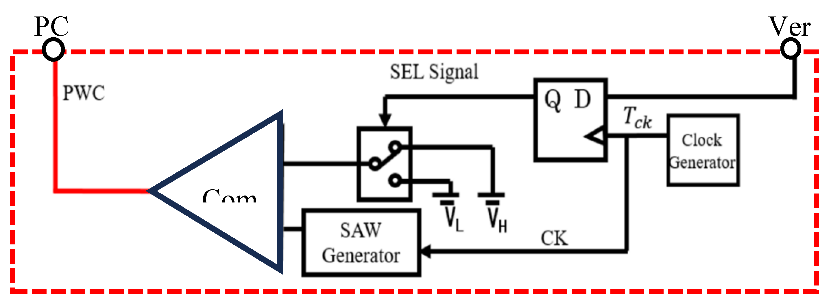
Figure 27.
Signal waveforms for PWC control.
In the PWC control, the analog output voltage error is converted to a digital signal and it modulates pulses. The converter output voltage is stabilized by appropriately switching these pulses. As a result, the noise spectrum is spread, and its notch is generated. Simulation shows the notch frequency ( ) is given as follows:
Fn = N / (WH ―WL) (24)
Hereafter, N is a positive integer throughout this paper. We observe that is determined by the difference of WH and WL and it is independent of the clock frequency. By adjusting WH and WL, can be set arbitrarily.
(C) Simulation Results of PWC Control
The pulse coded control regulates the converter output voltage using only two pulses, but without a saw-tooth signal. The clock frequency is set to exceed 500 kHz to ensure precise control of the output voltage, and other parameters are in Table 2.
The SAW peak voltage is set to 12V, to 9.6V and to 1.8V. Comparisons of and with the SAW under = 2μs results in of 1.6μs and of 0.3μs respectively. Figure 28 illustrates SEL and PWM signals, while Figure 29 displays the PWC signal the spectrum. The up-arrows indicate the clock, its double, and its triple frequencies. A notch is observed at 770 kHz), corresponding to the theoretical frequency from Eq. (24). Another notch is generated at 1.54 MHz, which corresponds to 2. However, this notch is not very prominent due to the high-frequency noises from the clock. Comparing the peak level at the clock frequency in Figure 8 with that in Figure 29, it is suppressed from 3.5 V to 1.1 V. Also, notches are produced.
4.2. Pulse Phase Coding (PPC) Control
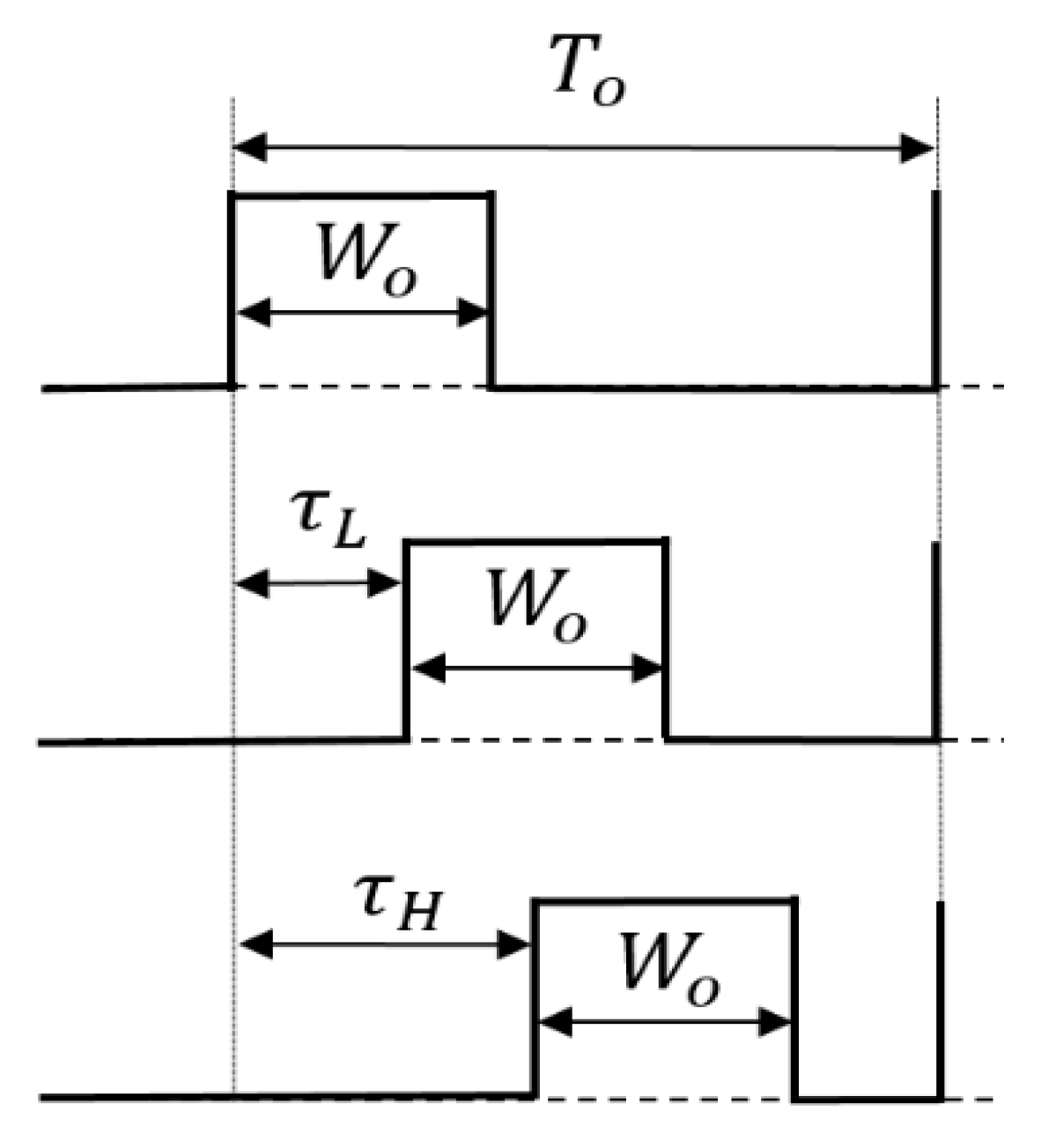
Pulse Phase Coding (PPC) control is realized with a delay circuit and a multiplexer (Figure 30). However, it does not alter D, and then it is used with the PWC system. Parameters are used for the notch frequency based on the empirical formula (Eq. (24)). Let τ represent the delay of pulse coding, with the longer delay and
the shorter one (Figure 31). The notch characteristics are also obtained using the PCC method. In case of a pulse train with a clock cycle of , the period T(k) of the k -th pulse is given by:
T(k) = +{τ(k) -τ(k-1)} (25)
We see that in the PPC method, the notch is dependent on also the previous pulse. Therefore, notches are unlikely produced because the coding cycle T(k) has 22 patterns. To address this, the following two periodic patterns can be utilized if alternate high/low coding is applied to the phase coding:
TH = T + {τH - τL}, TL = T - {τH - τL} (26)
We obtain Eq. (27) from Eqs. (24), (26) as follows:
Fnp = N /[2 ( τH - τL)] (27)
We see from Eq. (27) that the notch characteristics are determined by twice the difference in the pulse phases.
Figure 30.
PPC control circuit.
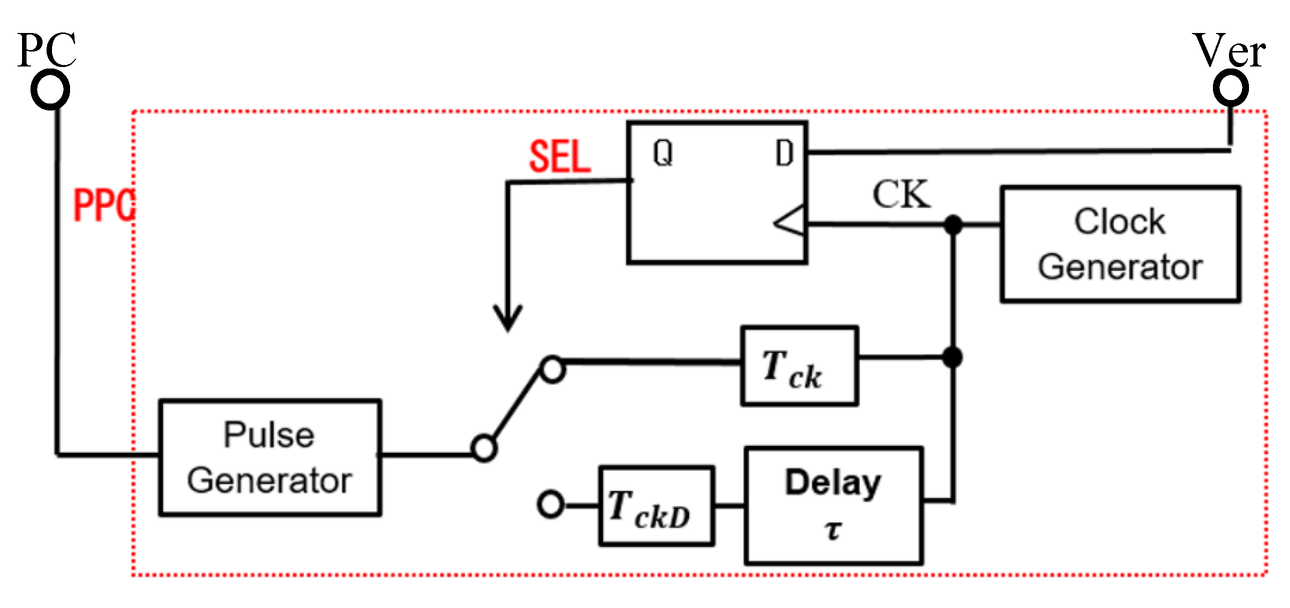
Figure 31.
Signals of PPC control.
4.3. Pulse Cycle Coding (PCC) Control
(A) PCC control circuit
In Figure 32, the duties of the two coded pulses differ as described by Eq. (26). Consequently, the duty cycle changes by altering the pulse period (Figure 33). Figure 34 shows an example of two pulses using the PCC method. There =0.4μs, =0.5s and =2.0s. Consequently, =0.8 and =0.2. The notch frequency in the spectrum of the PCD signal is given by
Fnc = N / (TL - TS ) (28)
Figure 32 shows the generator of these coded pulses. Pulses with different periods are generated from the pulse generation counter based on SEL (Figure 33). Here, and are defined as the pulse periods which are produced based on the SEL high and low states. By utilizing a differential circuit, a periodically modulated clock signal is generated. The generated saw-tooth is compared with and the PCC pulse is produced. Figure 34 shows signal waveforms associated with the pulse coding in the PCC system. The clock cycle varies depending on SEL, and the PCC signal synchronized with that cycle is the output.
Figure 32.
PCC control circuit.
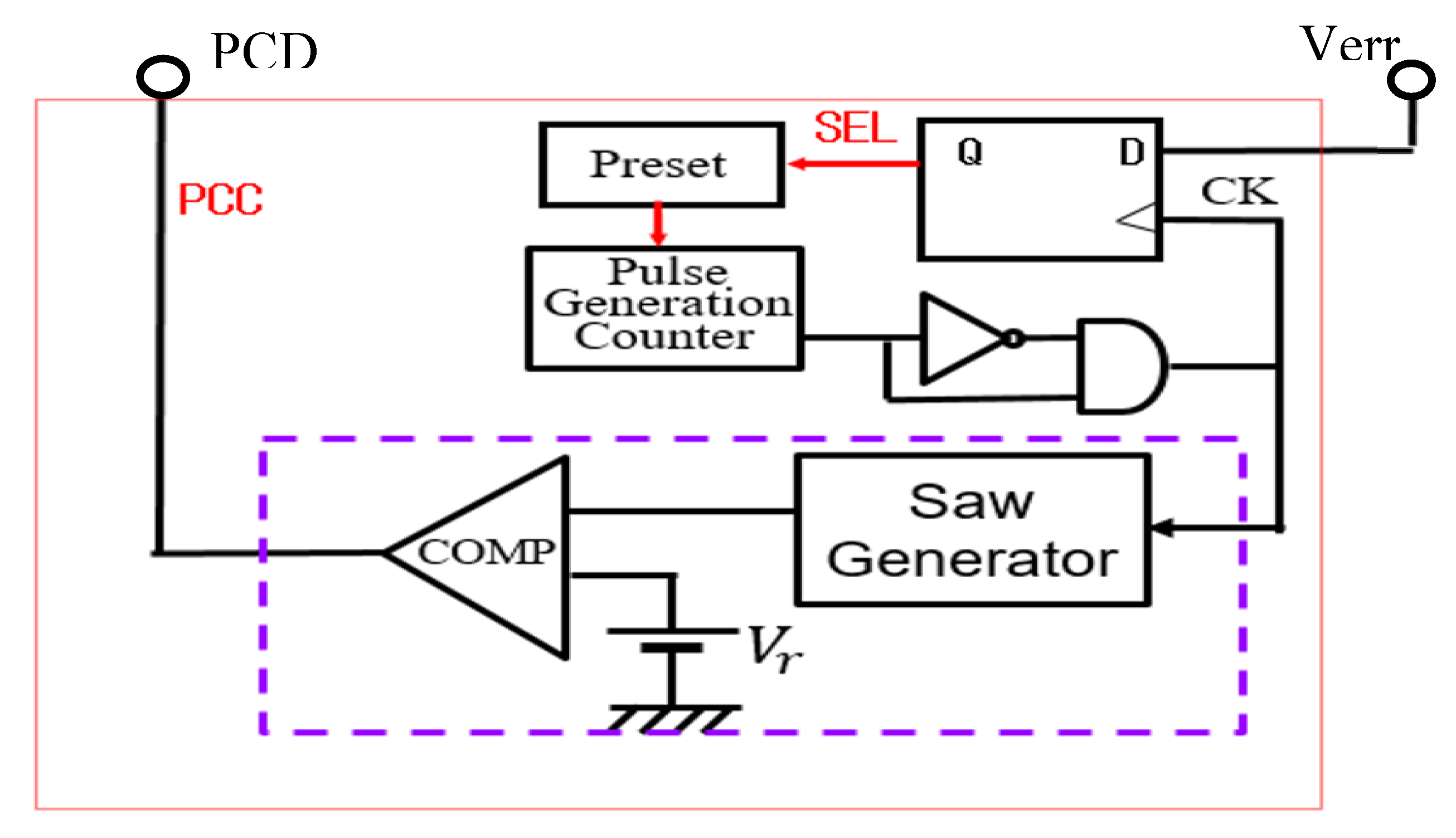
Figure 33.
PCD pulse of PCC control.
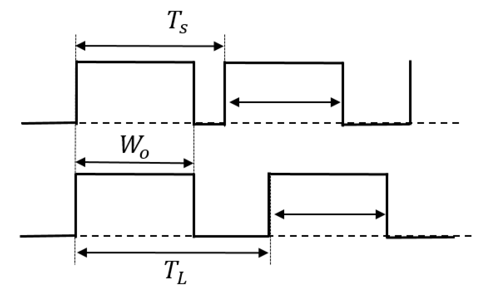
Figure 34.
Main waveforms of PCC control.
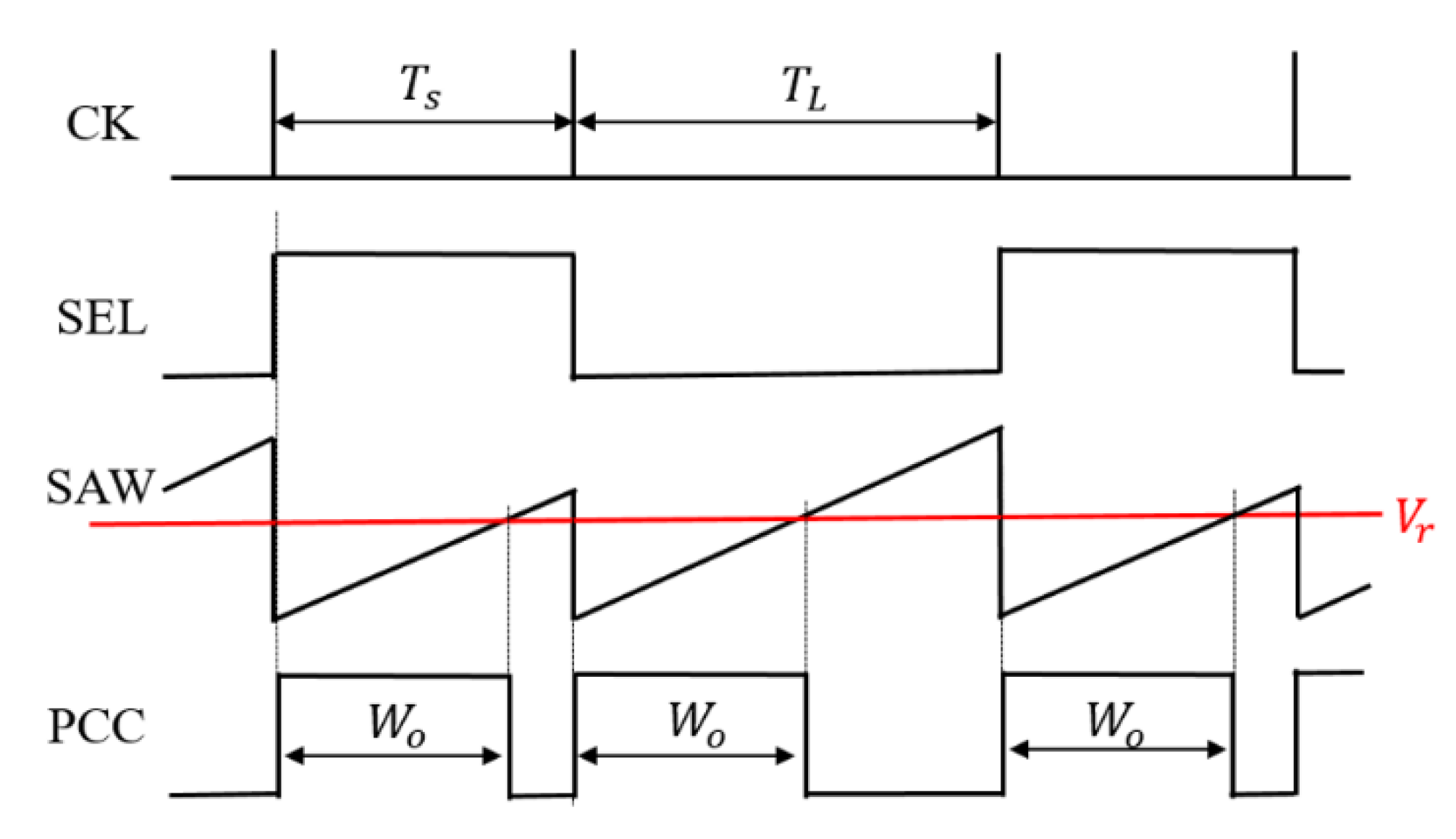
(B) Simulation Result with the PCC Control
Figure 35 illustrates main signals, and the pulse lengths of the PCC signal vary based on SEL. Figure 36 presents the simulated spectrum of the PCD signal with the PCC control. There the pulse conditions are =600 ns and =220 ns, resulting in a notch frequency of = 2.6 MHz, as calculated from Eq. (28). However, in Figure 36, notches appear around though they are not clearly visible. There are many line spectra because spread spectrum technique is not utilized. The frequency position of notch spectrum can be altered by the coded pulse frequencies or the switching converter parameters. Table 3 shows the simulation parameters.
4.4. Pulse Width and Phase Coding (PWPC) Control
(A) PWPC Method
The PWPC method is realized by incorporating a PPC circuit followed by the SAW generator for PWC (Figure 37). There the frequency for a large notch is designed using Eqs. (27) and (28). Figure 38 illustrates the SEL and PWPC signals. When SEL is high, is selected, and when SEL is low, the shifted is selected. It is observed that the notch by the PWPC method is deeper compared to the PWC method.
(B) Simulation Results with PWPC Control
In simulation, we set To=500 ns, WH=320 ns, WL=160 ns, τH=80 ns, τL=0 ns to produce a large notch at 6.25 MHz. Figure 39 illustrates the simulated spectrum of the PWPC signal. The noise level at the notch frequency is less than -20 dB relative to the average level.
4.5. Derivation of Notch Frequency Using Fourier Transform
Now we analyze various pulse coding methods and derive the formulae for their notch characteristics. We break down the analysis into four steps:
1) Define the signal of the pulse coding method.
2) Determine its Fourier transform.
3) Take its absolute value to obtain their spectrum characteristics.
4) Derive its zero point.
(A) Analysis of PWC Control
First, we analyze the PWC control. One period of the PWC signal is defined as , which has two different pulse widths: and (Figure 40). The zero frequency of the PWC control spectrum is obtained as Eqs. (29), (30), (31), using Fourier transform on the pair of coding pulses.
Then
Now we have the following:
We see that the PWC spectrum is expressed by a sinc function, which depends on the difference in pulse widths. The frequency at the zero point is obtained as follows:
Eq. (32) shows that the notch characteristics correspond to the zero of the sinc function. Notice that the notch frequency is determined by the difference in pulse widths, and it is independent of the clock frequency.
Next, calculate the spectrum characteristics of the eight rows of PWC pulses in Figure 41. Assume that the entire eight trains of pulses have a period , and the Fourier transform yields Eq. (33).
The calculated result of the notch frequency based on Eq. (33) is the same as that of Eq. (32).
The notch characteristics depend solely on the difference of pulse widths, regardless of the arrangement and number of pulses. The frequency at the zero point is obtained by:
Figure 42 illustrates a comparison between the sinc function and the spectrum of the PWC waveform with =3s, =7s, =250 kHz. The envelopes of the spectrum in simulation match the theoretical result (Eq. (35)).
(B) Analysis of PPC and PCC controls
We analyze the Pulse Position Coding (PPC) method. As illustrated in Figure 43, we define the PPC signal in one period as , which consists of two different phase pulse coding signals ( and ). The frequency characteristics of the PPC control are obtained by Fourier transform on the pair of coding pulses (Eq. (36)).
By taking the absolute value, Eq. (37) is derived, which shows the frequency at the zero point as Eq. (38):
According to Eqs. (37) and (38), the PPC method relies on two sinc functions, each exhibiting distinct notch characteristics. This method relies on the coding phase and the pulse width. Here, Eq. (38) represents the theoretical equation of the PPC method when alternating coding is employed.
Next, we analyze the PCC method. We define the PCC signal in one period as , which consists of two different cycle coding signals: and (Figure 44). The theoretical frequency of the PCC control is obtained as Eq. (39), by Fourier transform on the pair of coding pulses.
This equation shows that the notch characteristic depends on both the coding period and the pulse width, as in the PPC method.
(C) Analysis of PWPC method
Next, we analyze the Pulse Width and Phase Coding (PWPC) method, which encodes both the pulse width and phase. We define the PWPC signal in one period as , which represents two coding signals (Figure 45). The frequency characteristics of the PWPC control are derived as Eqs. (41) and (42).
In the PWPC, a sinc function with the pulse width and phase is used for representation, and two notch characteristics are generated. Further, if the notch characteristics are set to overlap with ∣, they become as follows:
Figure 46 provides a comparison of the notch characteristics in Eqs. (43) and (31). The notch around the zero point at 250 kHz in Eq. (43) is broader than in Eq. (38). The composite coding method increases both the notch width and depth compared to the PWC or PPC method.
5. Automatic Notch Generation [19,20,21,22,23,24,25]
This section describes the generation method of and for automatic notch generation in PWC control and PWPC control.
5.1. Automatic Notch Generation Using PWC Control
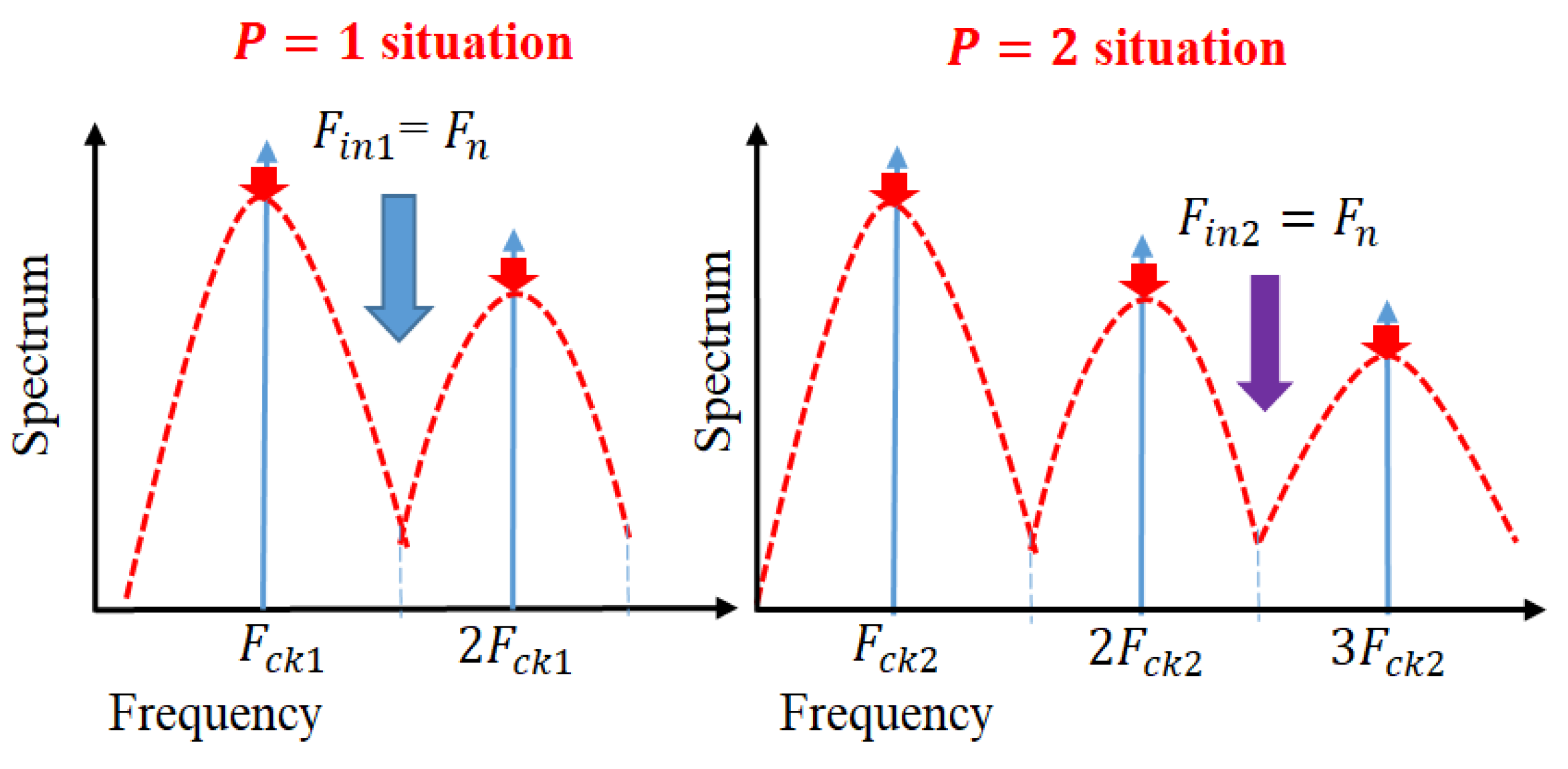
(A) Design of Relationship Among , and Our design is the generation of the notch frequency so that it lies between and 2 and it matches the received signal frequency (Figure 47). is provided to match the receiving frequency and the relationship among , and is given by Eq. (44). Here, P is a positive integer. Then, the relationship of (=and is given by Eq. (45).
We see from Eq. (44) that in case of P=1, is set between and 2, and it is equal to . In the case of P=2, is produced between and 3, and (Figure 47).
Figure 47.
Positions of [27] @IEICE.
Figure 47.
Positions of [27] @IEICE.
Conversely, the duty ratio D of the PWC signal is represented by Eqs. (46), (47), (48). Further, the original clock signal in Figure 48 represents the PWC signal that is not encoded, with a pulse width of . It also corresponds to Eq. (46), where is set to 0.5. Pulse-H and pulse-L are generated based on (Figure 48), and this corresponds to Eq. (47). Here, represents the difference of and , or of and . is determined by the difference of and . Also, , , and must satisfy the relationship given in Eq. (48) to ensure a stable output voltage, . Here, 2 = , and it is the difference of and .
(B) Automatic Notch Generation from Clock
is generated by as shown in Eq. (45). For P=1, the notch frequency is produced between and 2 from (See Figure 47). is shown in Eq. (49), which can be realized with a shifter and an adder. Figure 49a,b show the automatic PWC pulse coding circuit based on Eqs. (46), (47), (48) for , where and . Figure 49a shows the whole block diagram, while Figure 49b shows the detailed block diagram of Pulse-H, Pulse-L generation from and . Then, in the case of P=N, is produced between N and (N+1) with as shown in Eq. (50).
Figure 50 illustrates the automatic PWC method for P=N. For instance, in case N=2, is set to 1.25 MHz, is 500kHz and appears at 1.25 MHz, which falls between 2 and 3 .
(C) Simulation Results with Automatic Notch Generation
Digital circuit is used for coding pulse notch generation for (Figure 49). Figure 51 displays the waveforms of pulse-H and pulse-L for = 750 kHz. The saw-tooth period is automatically set to 2. By comparing and , pulse-L and pulse-H with and are generated automatically. According to Eq. (23), is 750 kHz, and the spectrum of the PWM signal is shown in Figure 52. The notch is at 750 kHz, which corresponds to , and there the bottom level is 1mV. However, there is the line spectrum at (= 500 kHz) with an amplitude of 900mV, and multiple harmonics spectra present. Thus, frequency modulation is considered for spectrum spread in the coding pulse notch generator.
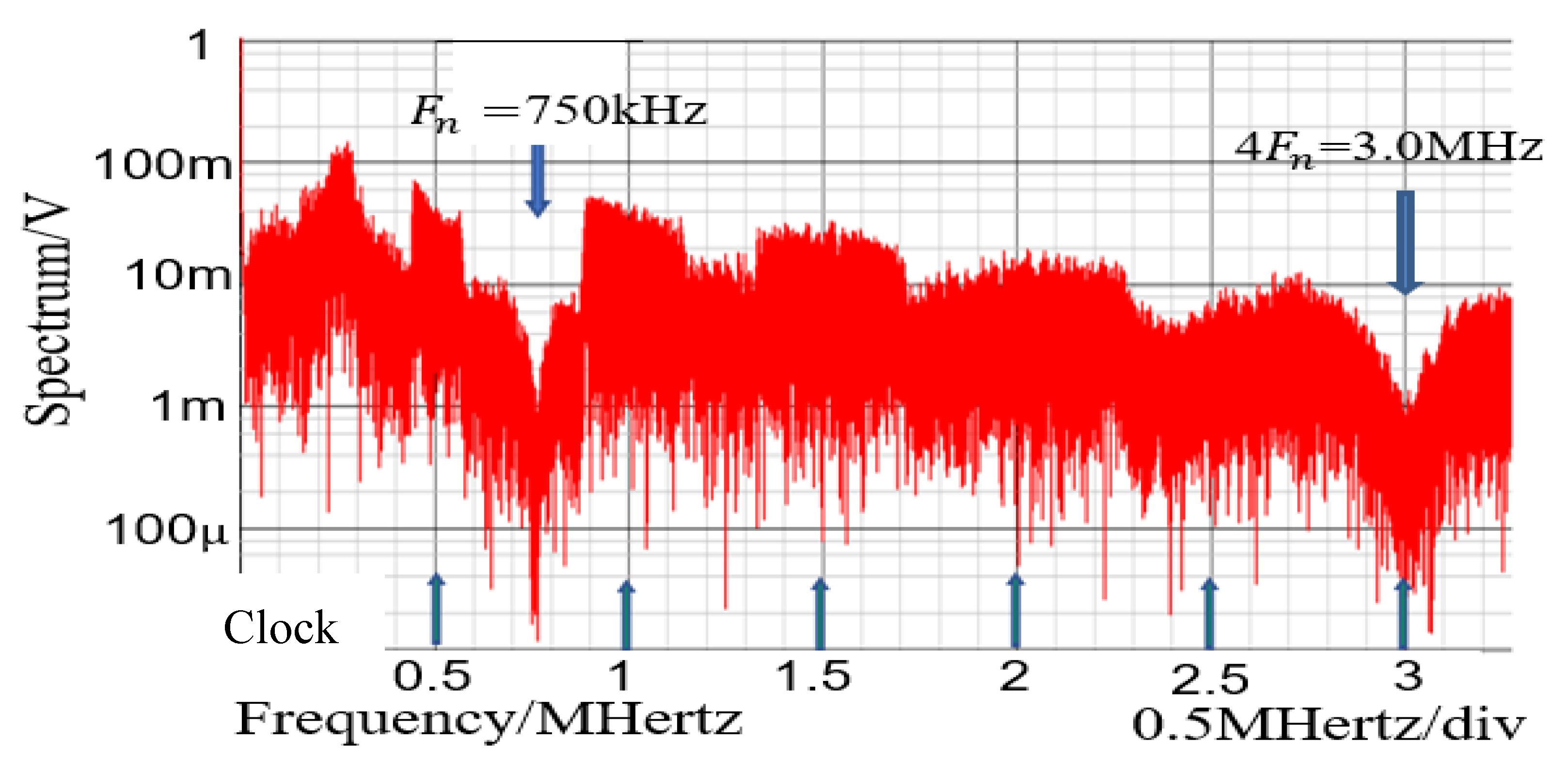
The frequency modulation of is used for EMI reduction as described in Section 3.1, and the spectrum of the PWM signal is displayed in Figure 53. The notch is clearly observed at 750 kHz (= . The bottom level of the notch frequency is 1mV, while the spectrum at (=500 kHz) is 20mV. Notice that another notch appears also at 4 in simulation. In principle, a 3MHz frequency is equal to 6(= 4). Since the clock and the input signal overlap, the notch is not expected to appear at 4. The theoretical reason for the notch cause at 4remains unknown and will be addressed in future work.
Figure 51.
Simulated waveforms for .
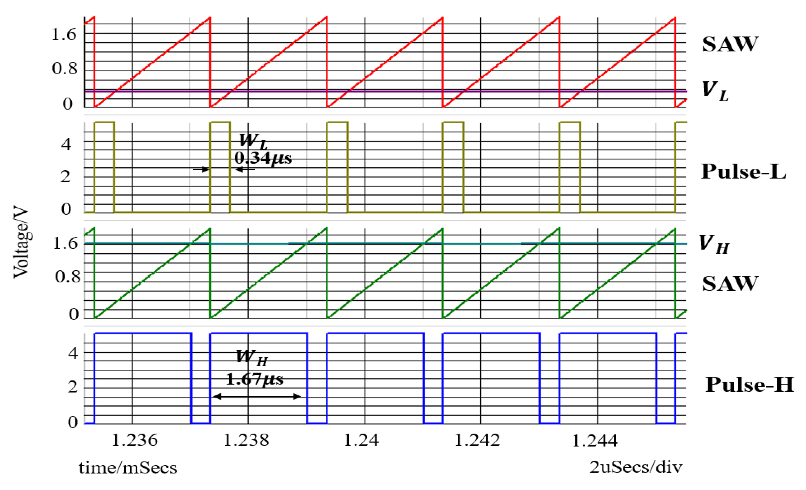
Figure 52.
Simulated spectrum of PWM signal without spread spectrum (P=1).
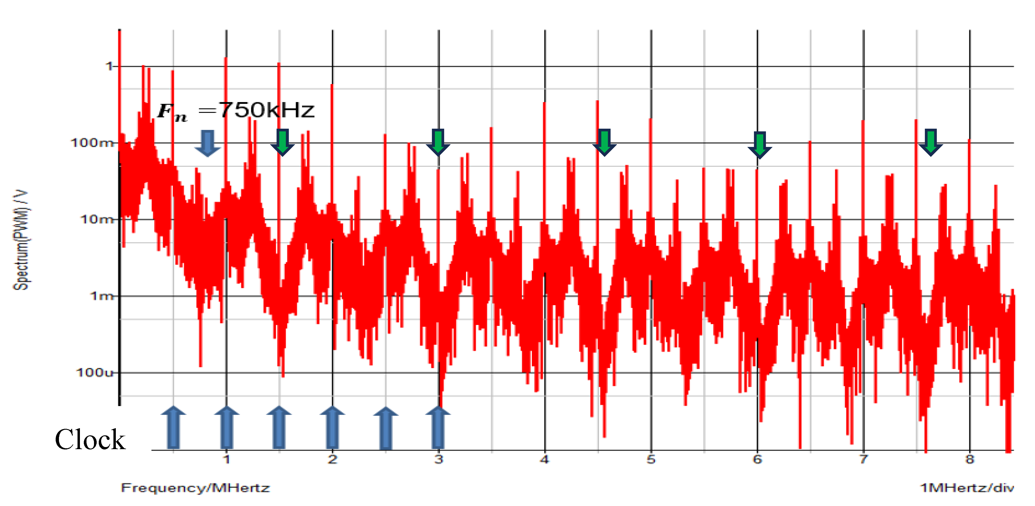
Figure 53.
Simulated spectrum with spread spectrum for .
Next, we discuss the case for P=2. Figure 54 displays the simulated waveforms of pulse-H and pulse-L for =1,250 kHz, and we observe and . The expected is 1,250 kHz based on Eq. (24). The spectrum of the PWM signal is displayed in Figure 55. The notch is observed at 1,270 kHz, which is equal to and falls between 2 and 3 .
Then, we consider the case for P=3. Figure 56 displays the simulated waveforms of pulse-H and pulse-L for =1,750 kHz. Also, and . Based on Eq. (24), is 1750 kHz. The spectrum of the PWM signal is displayed in Figure 57. The notch is observed at 1,750 kHz, which corresponds to and lies between 3 and 4 .
(D) Automatic Setting of Notch Frequency from Input Frequency
Here, we discuss the automatic adjustment of changes from channel 1 to channel 2 in the radio receiver (Figure 58). We set D = 0.5, P = 1, and of channel 1 to 750 kHz. Then the output of the automatic PWC controller produces a notch at 750 kHz. In case changes to 1,250 kHz, the corresponding , and also change, and the notch is automatically produced at 1,250 kHz. Simulated spectra are shown in Figure 59 and Figure 60, as changes from = 750 kHz to = 1,250 kHz. The notches are observed at 750 kHz and 1,250 kHz, which correspond to .
5.2. Automatic Notch Generation with PWPC Control
This subsection describes the automatic generation of Pulse-H, Pulse-L, and Pulse-LD for the PWPC control.
(A) Automatic Generation Method o PWPC Control
In the PWPC method, is given by Eqs. (24) and (27), and Figure 61 illustrates the PWPC configuration. There the automatic PWC controller generates NH and NL. Comparison of NH with the saw-tooth waveform produces Pulse-H, while comparison of NL with the delayed saw-tooth produces Pulse-LD. Figure 62 shows their waveforms, where the phase shift τ is equal to 0.5 and Eq. (24) is equal to Eq. (27) for the steep notch.
The relationship of and is given in Eq. (44). For P = 1, the followings are derived from Eq. (47). Here is the timing of the rear end of .
Figure 61.
Pulse coding circuit of the PWPC method.
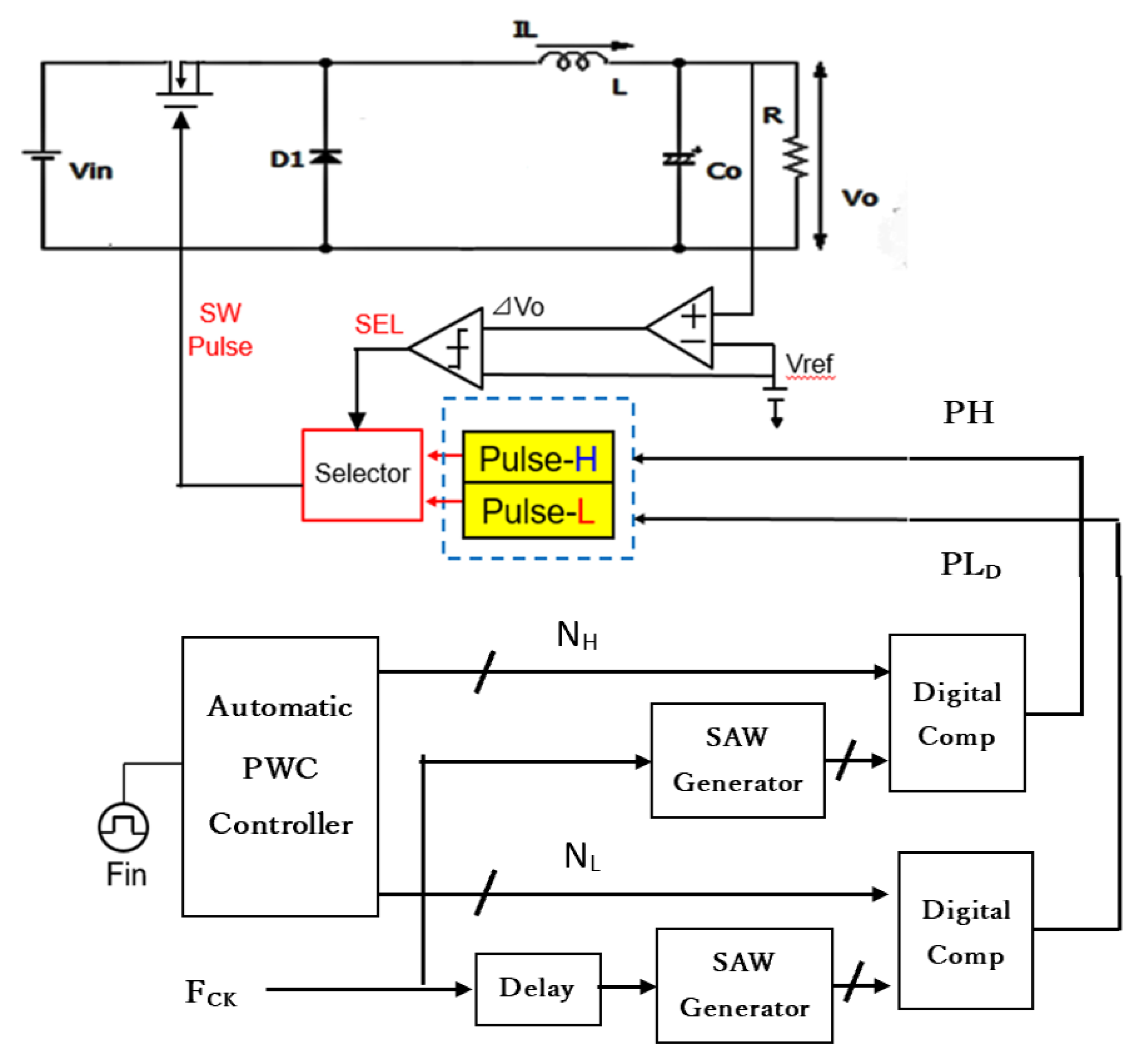
Figure 62.
Signals of PWPC control.
(B) Simulation Results of Automatic Notch Generation with PWPC Control
Figure 63 presents the saw-tooth signals, and the primary signals are highlighted in Figure 61. The coding pulses , and are generated by comparing and with the sawtooth and the delayed sawtooth signals.
There, is 10V, and is 5V. When is set to 750 kHz and for P=1, is set to 500 kHz. To set to = 750 kHz, =1.67,, and =0.67 are used based on Eq. (51).
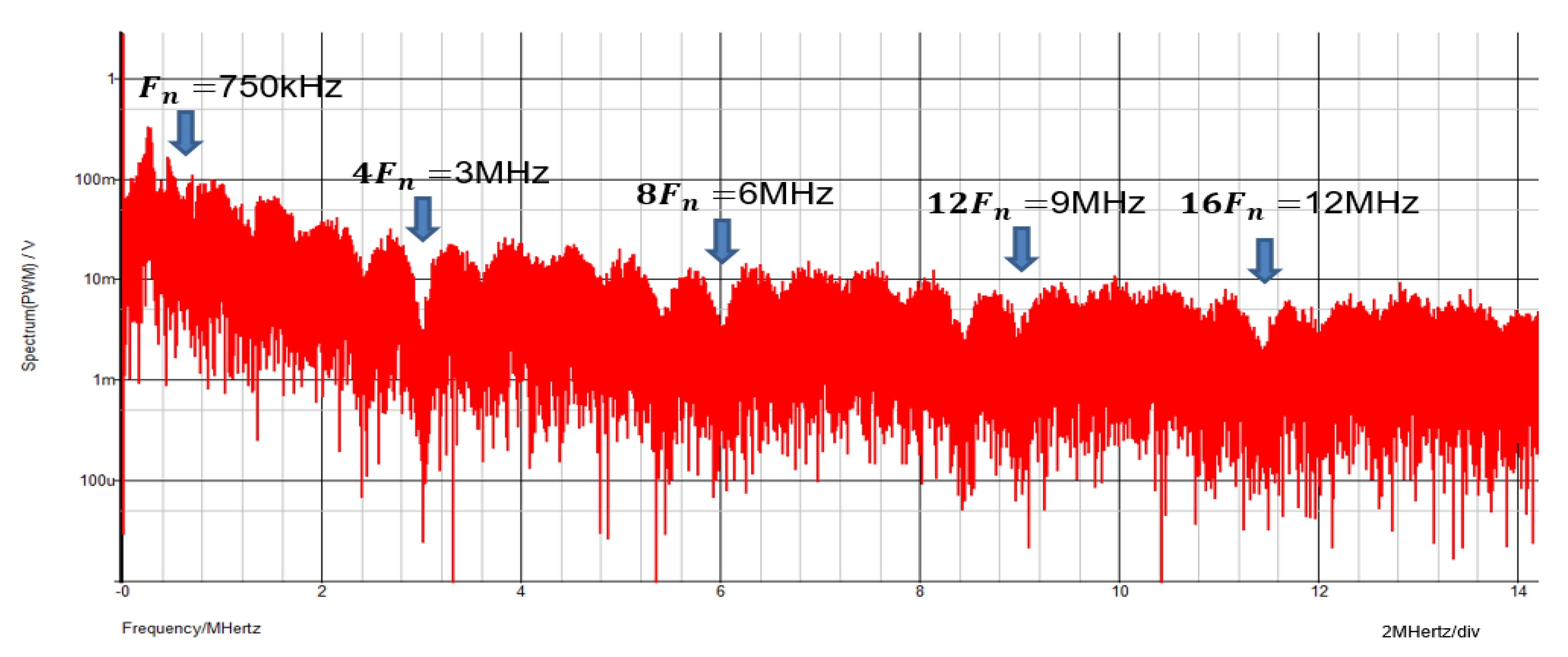
Simulation shows that with =1.67, =0.33, and =0.67 is 750 kHz (= ) (Figure 64 and Figure 65). A significant notch appears at 3.0 MHz (= 4 . Also, two notches are produced at higher frequencies.
Figure 63.
Saw-tooth signals with period and delay τ.
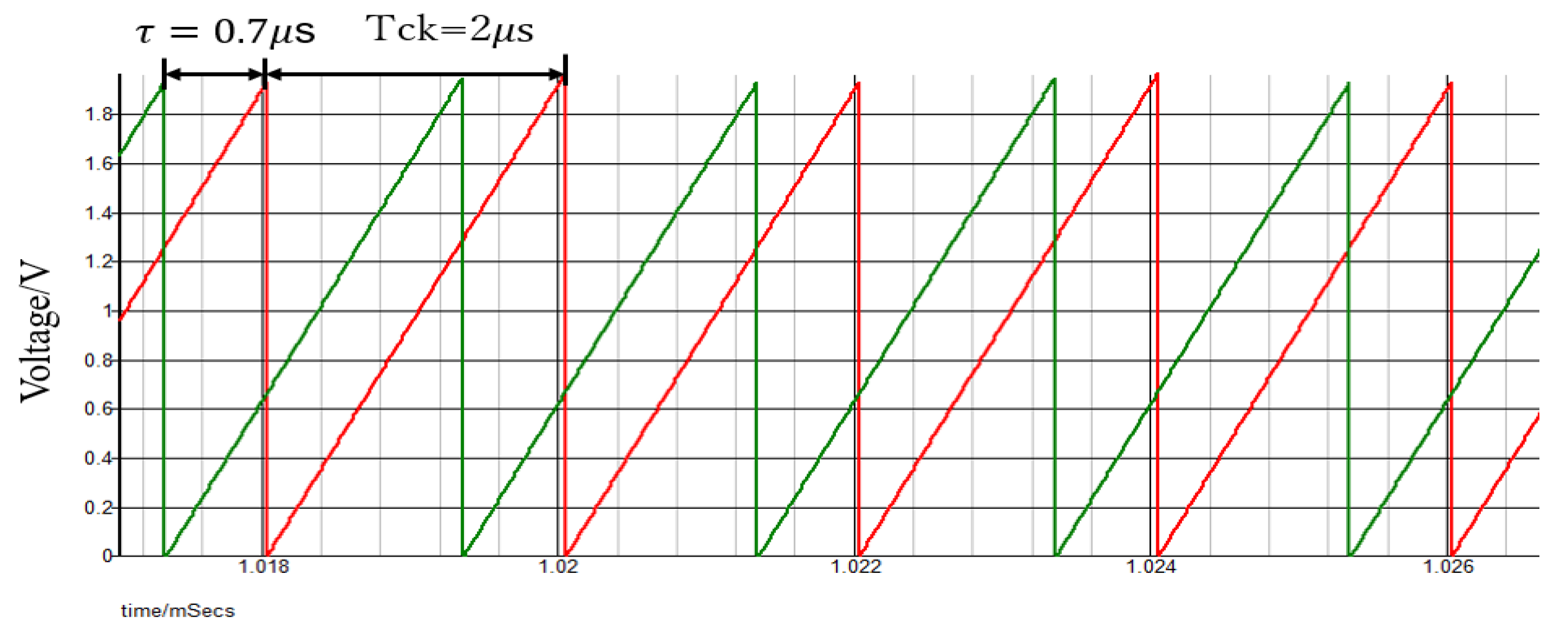
Figure 64.
Signals in PWPC circuit.
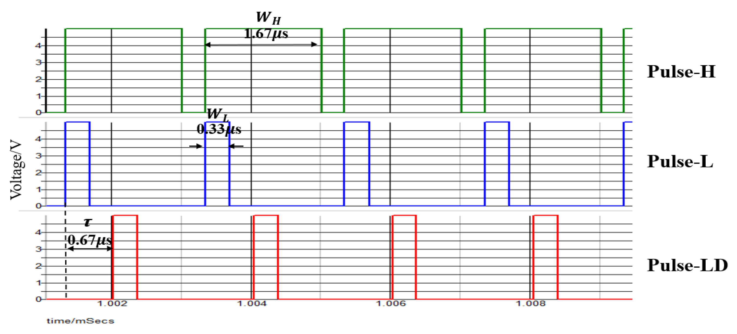
Figure 65.
Simulated spectrum with spread spectrum using PWPC method.
5.3. Duty Ratio Generation in Automatic Notch Generation
This subsection discusses a method to automatically detect and set D for and change.
Analysis of Relationship Between Voltage Conversion Ratio and PWM Duty Ratio
In the automatic PWC control, alone can generate as well as and using Eqs. (52), (53) based on Eqs. (45), (47), (48). Also see Figure 50. When (shift value of D), Tin is set to (2/3)Tck for P = 1 based on Eq. (45).
When varies, the duty cycle of SEL, is affected, which influences , and the resulting duty ratio is represented by Eq. (54). During the circuit design, the Vo/Vi ratio is fixed, meaning , and are set. Even if is changed, and are still produced automatically by the circuit. However, when Vo is changed, also is changed, which differs from the designed .
For instance, for and , we set D=Vo/Vi=5V/10V=0.5. That is, for and based on Eqs. (52) and (53), and =0.5, the waveform of and remains balanced. However, when varies, changes to 0.86 and changes to 0.20. In the designed circuit, when remains at 0.5, is increased while is decreased.
In Eq. (54), ∆D represents the variation of D, and the change rate is defined as x=ΔD/D. Then, the changed and , along with and , are given by Eqs. (55) to (58).
Before D varies, =0.5 and . This means that the select signal keeps and balanced. After D varies, can be given by Eq. (59). The average voltage of the SEL signal, is given by Eq. (60), and is influenced by . Consequently, when changes, increases.
It is inferred that when the duty ratio shifts from D to D’, changes to while changes to . Consequently, the select signal for and is no longer balanced. It influences VSEL, shifting it from Vcc/2 to Vcc (1−ΔD/D)/2. Consequently, the output voltage also increases.
(B) Simulation Results of Duty Ratio Change
According to Section 5.2, when is varied while keeping and fixed, the duty cycle of SEL changes significantly. This causes significant variations in and . In simulation, 5.0V and are altered to 10V and 15V. Correspondingly, D changes to 0.5 and 0.33. Figure 66 displays the select signal waveforms. It is observed that for = 0.5, the waveforms of and remain balanced. For D = 0.33, the waveform of the select signal becomes unbalanced, and the output of exceeds that of Figure 67 illustrates as varies. Any change in D affects .
(C) Automatic Detection of PWM Duty
Based on D and Eqs. (52), (53), and are generated (Figure 49). When varies, D also varies according to the ratio D=Vo/Vi. The number of and pulses are automatically adjusted based on D. Detection method of the SAW peak voltage produced by and Vi is considered. Under this condition, the peak voltage is proportional to D.
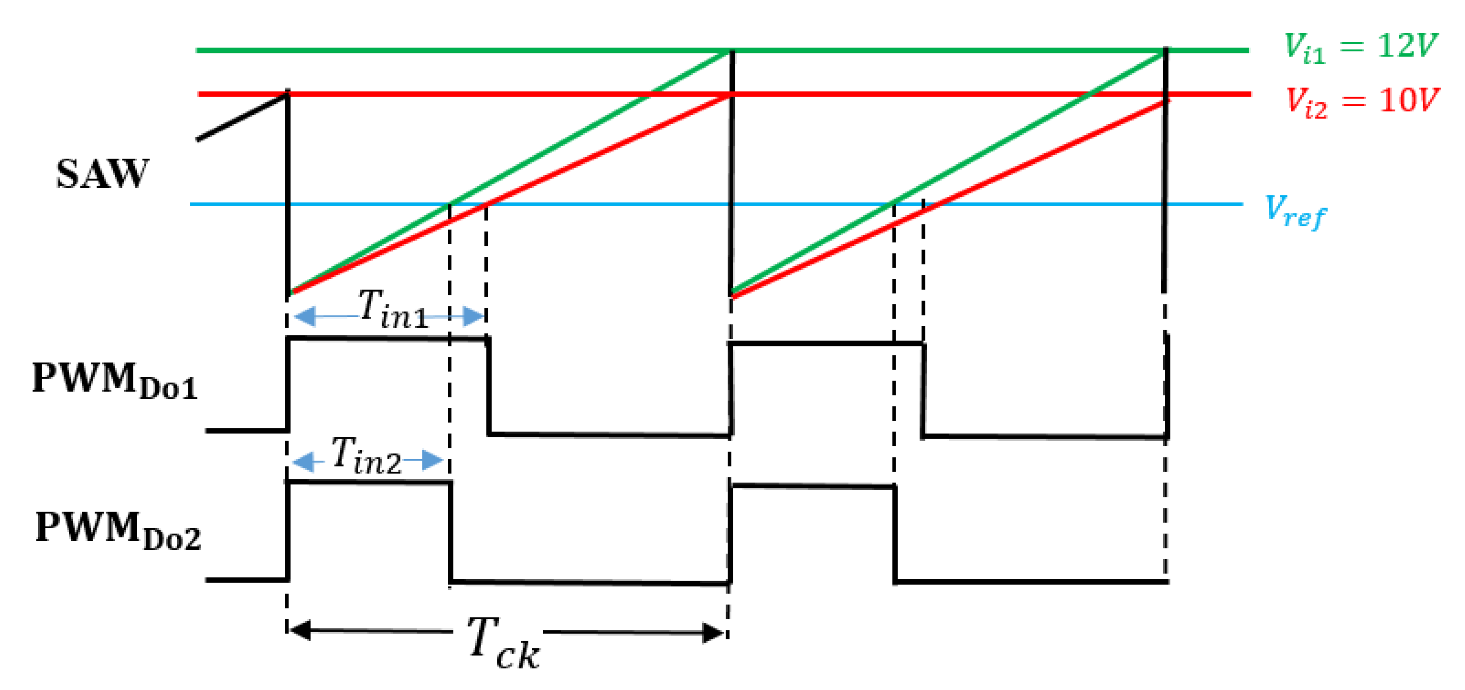
Figure 68 illustrates the automatic D detection circuit. There, the SAW signal is generated by a current source, with the frequency of the SAW designated as . A voltage follower serves as the peak hold circuit, and the peak voltage is compared with by an error amplifier and an error voltage is generated. Usage of a voltage-controlled current source converts the error voltage into an error current, which is then fed-back to the SAW generator. In this process, the SAW peak voltage is automatically detected, which is equal to . Then, the comparator produces the D detection signal by comparing the SAW signal with , which is equal to .
Figure 69 shows signal waveforms of the D detection circuit. For , the SAW peak voltage is 12V. By comparing the SAW with , the sampled data corresponds to . For = 10V, the SAW peak voltage automatically changes to 10V. By comparing the SAW and , the sampled data becomes .
Figure 68.
Automatic D detection circuit [26] @IEEE.
Figure 68.
Automatic D detection circuit [26] @IEEE.
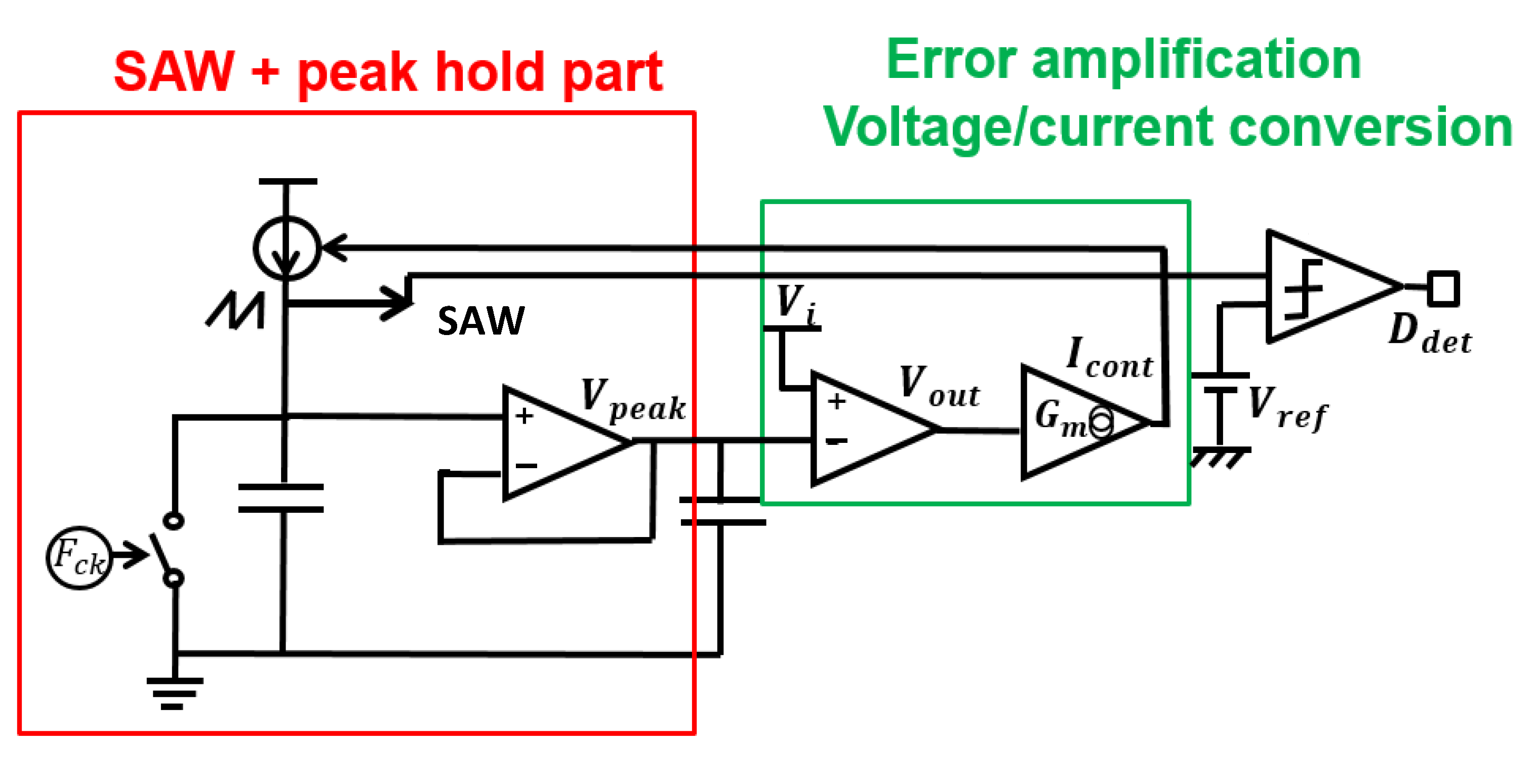
Figure 69.
Signals of detection circuit [26] @IEEE.
Figure 69.
Signals of detection circuit [26] @IEEE.
We have developed automatic notch frequency generator using this method. There, is automatically detected in response to change, for the notch creation at the input frequency. The simulation results are shown in Figure 70, with the same parameters as those in Section 5.1, except for , which is 15V this time. Additionally, the clock is not modulated, and D can be automatically detected as 0.33. The simulation results show that the notch is at 750 kHz (= ).
The SEL signal is illustrated in Figure 71. In comparison to Figure 66, under the condition of D=0.33, the waveform of and remains balanced. The output voltage ripple is displayed in Figure 72, that is decreased from 8.5 mV to 1.1 mV, compared with Figure 67.
The above discussion says that for setting D (0.33 < D < 0.67) in automatic notch generation with the PWC control and the D automatic detection method, D is detected based on the change in . This results in a notch being produced at , while reducing .
6. Implementation of PWC Controlled Converter with Notch Generation
6.1. Experiment of Converter with Notch Generation
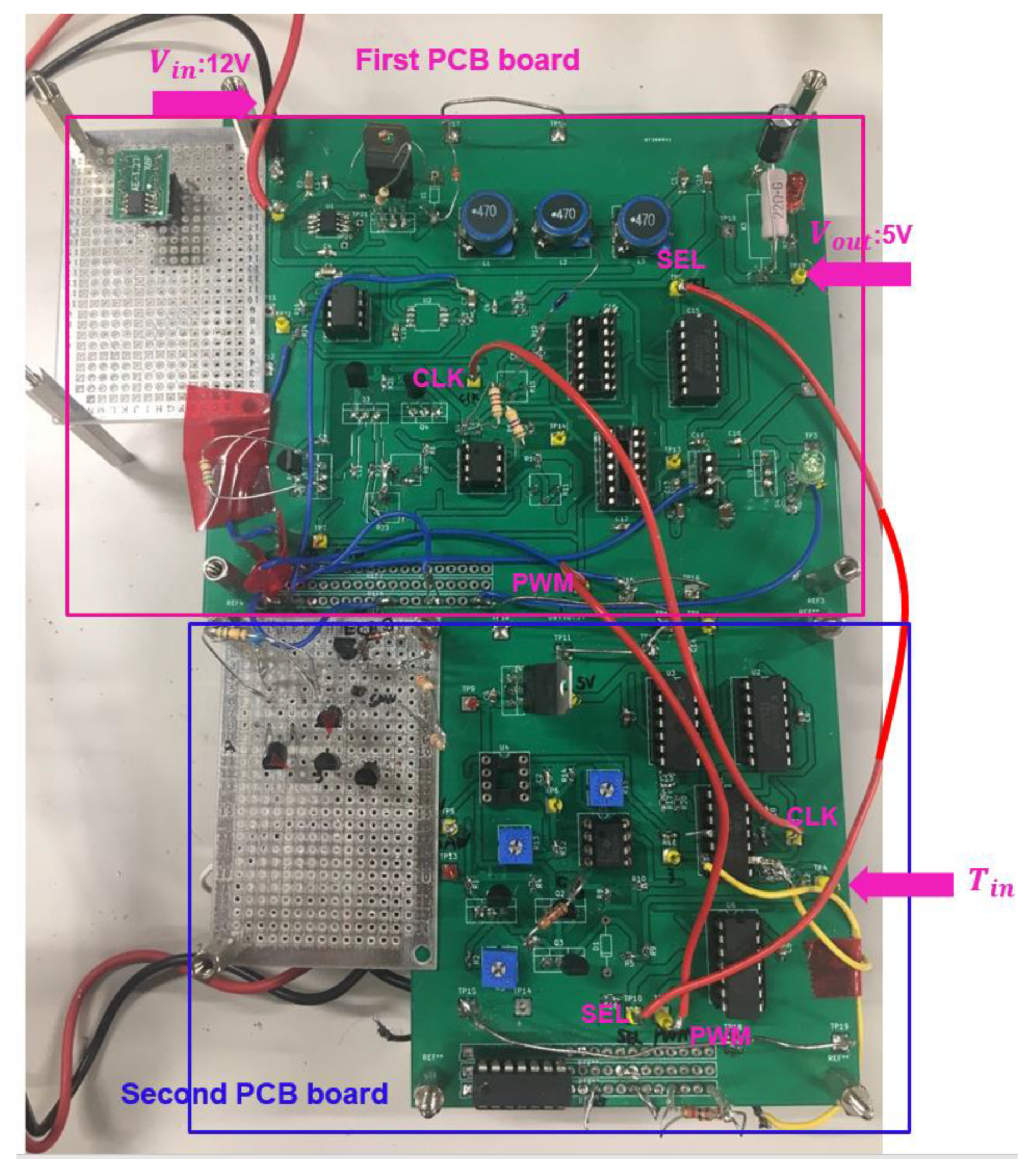
We have verified the notch frequency using the PWC control with the prototype circuit in Figure 73, with the parameters in Table 4. Figure 74 shows its implemented prototype on a PCB board.
Figure 75 shows measured waveforms of and . Additionally, we have analyzed the spectrum of the PWC control converter with and (Figure 76). The notches appear between and 2 , between 2 and 3 , and between 3 and 4 . By substituting the parameter values into Eq. (24), 1.66 MHz is obtained, which agrees with the measured result.
6.2. Experiment of Automatic Notch Generation
Experiments examine the notch characteristics using the prototype circuit.
(A) Experiment Method of Automatic Notch Generation
In the automatic notch generation method, the control stage circuit corresponds to the one in Figure 49. We expect that by inputting , the notch is automatically produced at . We have . In 1.5 frequency generation circuit (pink border), just the input a pulse with a period of produces . The waveforms of , , , and are illustrated in Figure 77. By comparing the saw-tooth waveform with to and , and are generated respectively.
Figure 78 shows the prototype with three red wires connecting the two boards. By inputting a pulse with a period of using a pulse generator, a notch is produced automatically at the same frequency. Next, we evaluate the prototype circuit with the parameters in Table 5.
For the first example, we set P = 1 in Eq. (44), and a notch is produced between and 2 . We input = 400 kHz, can be automatically about 267kHz ( ) and (Figure 79a). The PWM and SEL signals are shown in Figure 79b. Based on Eq. (24), the notch frequency is calculated as 435 kHz. From the experimental spectrum, the observed notch frequency is approximately 400 kHz, which closely matches the theoretical result by Eq. (24), and lies between and 2 .
Figure 77.
Signals when produces .
Figure 78.
Prototype for automatic notch generation.
(B) Experimental Results of Automatic Notch Generation
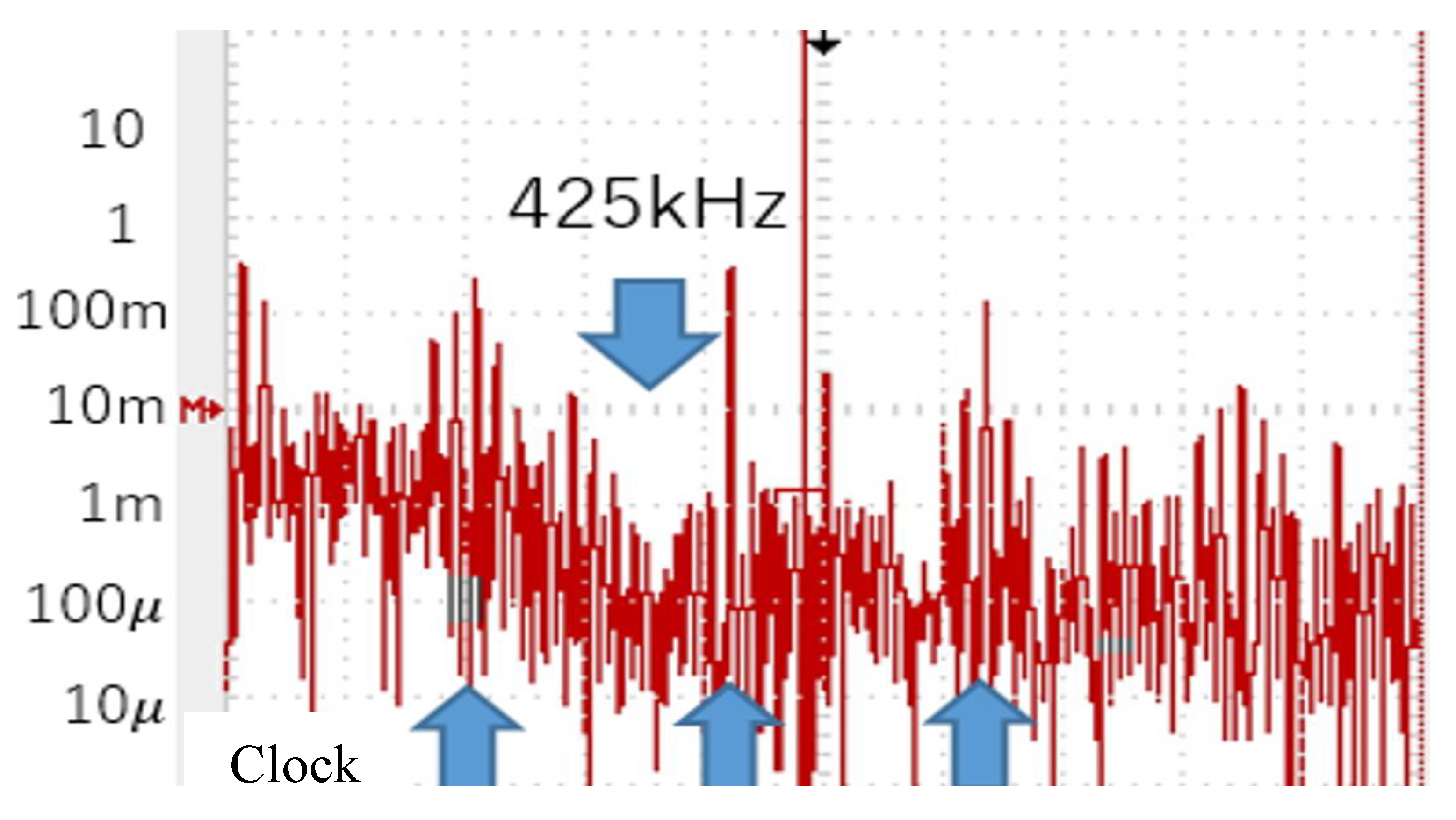
When is 400 kHz, is automatically set to 267 kHz ( = 3.7 μs) for P=1. The pulse widths are automatically adjusted to = 3.0 μs and = 0.7 μs (Figure 79a). The PWM and SEL signals are illustrated in Figure 79b. can be calculated as 435 kHz based on Eq. (30). The experiments show that the observed is around 425 kHz (Figure 80), which matches the theoretical result in Eq. (30), and that this notch lies between and .
Figure 79.
Measured waveforms ().
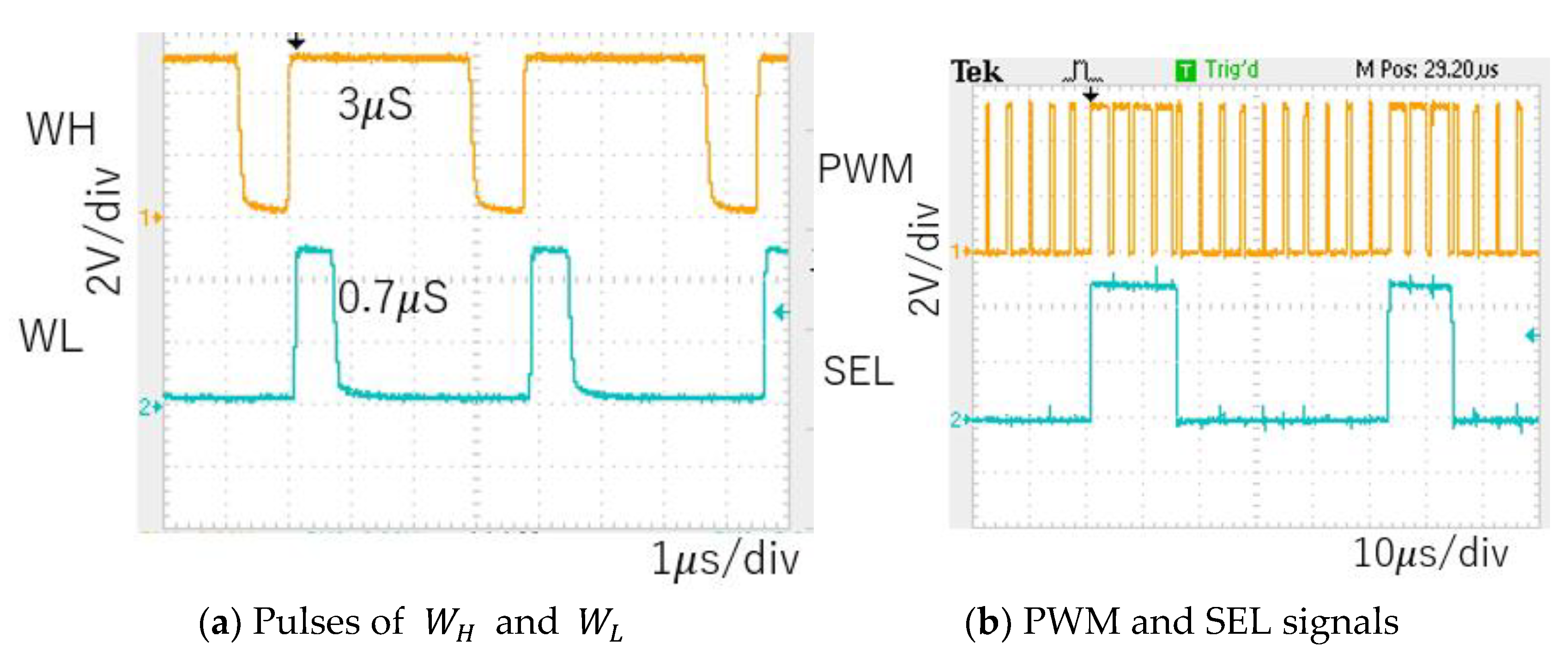
Figure 80.
Measured spectrum of PWM signal ().
For the second example, still P=1 is used. By changing to 600 kHz, can be automatically adjusted to 400 kHz ( ). Consequently, and (Figure 81a). The PWM and SEL signals are illustrated in Figure 81b. is calculated as 666 kHz based on Eq. (24), and the experimental results show that the observed notch is at 666 kHz (Figure 82), which lies between and .
7. Conclusion
This paper reviews technologies to realize the selectable band in the EMI noise spread spectrum of the DC-DC switching converter. The EMI noise is diffused from the switching signals caused by the clock, and then the noise spectrum spread techniques with the selectable notch band at the undesirable frequency such as the receiving radio signal band have been developed.
First, we review the configuration and operation of fundamental DC-DC switching converters of buck, boost and buck-boost types. They radiate some amount of EMI noise from the PWM signal with the line spectra at the frequencies of the clock and its harmonics.
Next, we introduce the conventional spread spectrum method that shakes the clock frequency and phase to reduce the line spectrum levels.
In addition to basic analog modulation methods, an analog noise generator using bit-inverse and bit-exchange in conjunction with an LFSR is explained. These spread spectrum techniques disperse noise power into unwanted frequencies. For example, in weak radio wave receivers, the dispersion of noise into the reception frequency band is undesirable.
Then we review the Pulse Coding Driving (PCD) control method, which significantly reduces the noise level at the selected frequency band. Instead of controlling the output voltage with the PWM signal, it controls the output voltage using two different pulse counts such as Pulse Width Coding (PWC) method, Pulse Phase Coding (PPC) method, Pulse Width and Phase Coding method. Also, the theoretical derivation of the notch frequencies is shown. The PCD control can be used in conjunction with the PWM control.
Further, a PCD control method that automatically tracks changes in the receiving frequency and the input voltage is introduced. The receiving frequency is often switched in the radio receiver and the input frequency fluctuates. There, the notch band characteristics need to automatically switch to another reception band. We explain a method to detect the received frequency and automatically switch the clock frequency to the proper one, as well as a method so that for the input voltage change, the PCD control automatically sets two types of pulse counts, while the conventional method automatically controls the duty of the PWM signal.
Finally, we review a PWC control method for automatic notch generation, with the notch characteristics of two types of PCD pulses and their spectra. There the PCD pulses and the switching of notch frequencies are changed when the reception frequency is switched.
Acknowledgments
All members and research collaborators in our laboratory who contributed to the research described in this paper are acknowledged.
References
- K. Harada, T. Ninomiya, and B. Gu, Circuit Scheme of PWM Converter in Basics of Switching Converter, Corona Publishing, Japan (1992).
- A. J. Stratakos, C. R. Sullivan, S. R. Sandersand, R. W. Broderson, “High-Efficiency Low-Voltage DC-DC Conversion for Portable Applications in Low-Voltage/Low-Power Integrated Circuits and Systems,” Chapter 12, IEEE Press (1999).
- A. M. Trzynadlowski, Z. Wang, J. M. Nagashima, C. Stancu, and M. H. Zelechowsk, “Comparative Investigation of PWM Techniques for a New Drive for Electric Vehicles,” IEEE Trans. Ind. Appl, vol. 39, no. 5, pp. 1396-1403 (Sep. 2003).
- Robert W. Erickson, Dragan Maksimović, Fundamentals of Power Electronics, The Third Edition, Springer (2020).
- K. Taniguchi, T. Sato, T. Nabeshima and K. Nishijima, “Constant frequency hysteretic PWM controlled buck converter,” International Conference on Power Electronics and Drive Systems (PEDS), pp. 1194-1199 Taipei, Taiwan, (2009).
- R. Lai, Y. Maillet, F. Wang, S. Wang, R. Burgos, and D. Boroyevich, “An Integrated EMI Choke for Differential-mode and Common-mode Noise Suppression,” IEEE Trans. Power Electron, vol.25, no.3, pp. 539-544 (March 2010).
- R. Mukherjee, A. Patra, and S. Banerjee “Impact of a Frequency Modulated Pulse Width Modulation (PWM) Switching Converter on the Input Power System Quality,” IEEE Trans. Power Electron., vol.25, no.6, pp. 1450-1459 (Jun. 2010).
- A. M. Stankovic, G. C. Verghese, and D. J. Perreault, “Analysis and Synthesis of Randomized Modulation Schemes for Power Converters,” IEEE Trans. Power Electron, vol. 10, no. 6, pp. 680–693 (Nov. 1995).
- K. K. Tse, H. S. Chung, S. Y. Hui, and H. C. So, “Analysis and Spectral Characteristics of a Spread-Spectrum Technique for Conducted EMI Suppression,” IEEE Trans. Power Electron., vol.15, no.2, pp. 399-410 (Mar. 2000).
- H. Giral, E. A. Aroudi, L. Martinez-Salamero, R. Leyva, and J. Maixe, “Current Control Technique for Improving EMC in Power Converters,” Electron. Lett., vol.37, no.5 (Mar. 2001).
- B. Yuan, C. Liang, Z. Li and Q. Zhang, “A Clock Generator with Dual Pseudo Random Spread Spectrum in DC-DC Buck Converter,” IEEE International Conference on Integrated Circuits, Technologies and Applications (ICTA), Hangzhou, China, pp. 2024.
- F. Mihali, and D. Kos, “Reduced Conductive EMI in Switched-mode DC–DC Power Converters without EMI Filters: PWM versus Randomized PWM,” IEEE Trans. Power Electron, vol.21, no.6, pp. 1783-1794 (Nov. 2006).
- H. Li, W. K. S. Tang, Z. Li, and W. A. Halang, “A Chaotic Peak Current Mode Boost Converter for EMI Reduction and Ripple Suppression,” IEEE Trans. Circuits Syst. II: Exp. Briefs, vol.55, no.8, pp. 763-767 (Aug. 2008).
- Y. -H. Kao et al., “8.11 A 48V-to-5V Buck Converter with Triple EMI Suppression Circuit Meeting CISPR 25 Automotive Standards,” IEEE International Solid-State Circuits Conference (ISSCC), pp. 164-166, San Francisco, CA, USA (Feb. 2024).
- M. Fishta, E. Raviola and F. Fiori, “EMI Reduction at the Source in WBG Inverters: A Comparative Study of Spread-Spectrum Modulation and Auxiliary Switching Leg Techniques,” IEEE Transactions on Electromagnetic Compatibility, vol. 66, no. 5, pp. 1412-1419 (Oct. 2024).
- E. Stok, M. Otten, H. Huisman and Y. Kösesoy, “EMI Reduction in an Interleaved Buck Converter Through Spread Spectrum Frequency Modulation,” 25th European Conference on Power Electronics and Applications (EPE’23 ECCE Europe), pp. 1-11, Aalborg, Denmark (2023).
- T. -W. Sun, M. -Z. Li, T. -H. Tsai and C. -C. Chang, “A High-Accuracy Hysteretic DC-DC Converter Using A Spread-Spectrum EMI Suppression Technique with Double Gold Codes,” 21st IEEE Interregional NEWCAS Conference (NEWCAS), pp. 1-4, Edinburgh, United Kingdom (2023).
- A. Barbaro, M. Fishta, E. Raviola and F. Fiori, “A Comparison of Spread Spectrum and Sigma Delta Modulations to Mitigate Conducted EMI in GaN-Based DC-DC Converters,” 14th International Workshop on the Electromagnetic Compatibility of Integrated Circuits (EMC Compo), pp. 1-6, Torino, Italy (2024).
- J. Kundrata and A. Baric, “Clock Frequency Optimization of a Compensated Spread-Spectrum Controller in Buck Converters,” IEEE Access, vol. 12, pp. 4881.
- S. Kapat, “Reconfigurable Periodic Bi-frequency DPWM with Custom Harmonic Reduction in DC-DC Converters,” IEEE Trans. Power Electron, vol.31, no.4, (Apr. 2016).
- J. Kundrata and A. Barić, “Implementation of Voltage Regulation in a Spread-Spectrum-Clocked Buck Converter,” 46th MIPRO ICT and Electronics Convention (MIPRO), pp. 253-258, Opatija, Croatia (2023).
- N. Miki, N. Tsukiji, K. Asaishi, Y. Kobori, N. Takai, H. Kobayashi, “EMI Reduction Technique With Noise Spread Spectrum Using Swept Frequency Modulation for Hysteretic DC-DC Converters,” IEEE International Symposium on Intelligent Signal Processing and Communication Systems (ISPACS), Xiamen, China (Nov. 6-9, 2017).
- N. Oiwa, S. Sakurai, Y. Sun, M. T. Tri, J. Li, Y. Kobori, H. Kobayashi, “EMI Noise Reduction for PFC Converter with Improved Efficiency and High Frequency Clock,” IEEE 14th International Conference on Solid-State and Integrated Circuit Technology, Qingdao, China (Nov. 2018.
- Y. Kobori, Y. Sun, M. T. Tri, A. Kuwana, H. Kobayashi, “EMI Reduction in Switching Converters With Pseudo Random Analog Noise,” Journal of Technology and Social Science, Vol.4, No.2, pp.33-48 (20). 20 April.
- Y. Kobori, T. Arafune, N. Tsukiji, H. Kobayashi, “Selectable Notch Frequencies of EMI Spread Spectrum Using Pulse Modulation in Switching Converter,” IEEE 11th International Conference on ASIC, no.16158097, B8-8, Chengdu, China (Nov. 2015).
- Y. Sun, Y. Kobori, H. Kobayashi, “Full Automatic Notch Generation in Noise Spectrum of Pulse Coding Controlled Switching Converter,” IEEE 14th International Conference on Solid-State and Integrated Circuit Technology, Qingdao, China (Nov. 2018.
- Y. Sun, Y. Kobori, A. Kuwana, H. Kobayashi, “Pulse Coding Controlled Switching Converter that Generates Notch Frequency to Suit Noise Spectrum,” IEICE Trans. Communications, Vol.E103-B, No.11, pp.1331-1340 (Nov. 2020).
- G. Dong, S. Katayama, Y. Sun, Y. Kobori, A. Kuwana, H. Kobayashi, “Notch Frequency Generation Methods in Noise Spread Spectrum for Pulse Coding Switching DC-DC Converter,” 13th Latin American Symposium on Circuits and Systems, Santiago, Chile (Mar. 2022).
- A. T. L. Lee, W. Jin, S.-C. Tan, and R. S. Y. Hui, Single-Inductor Multiple-Output Converters: Topologies, Implementation, and Applications, CRC Press; 1st edition (Dec. 2021).
- B. Rooholahi, Y. P. Siwakoti, H. -G. Eckel, F. Blaabjerg and A. S. Bahman, “Enhanced Single-Inductor Single-Input Dual-Output DC–DC Converter With Voltage Balancing Capability,” IEEE Transactions on Industrial Electronics, vol. 71, no. 7, pp. 7241-7251, (24). 20 July.
- X. Zhang, A. Zhao, X. Li, Y. Jiang, R. P. Martins and P. -I. Mak, “An 80W Single-Inductor DC-DC Architecture for Simultaneous Flash Charging and Dual-Output PoL Supply with 92.1% Peak Efficiency from 15V-to-28V Input to 12.6V/3.3V/1V Outputs Using 1.3 mm3 Inductor,” IEEE European Solid-State Electronics Research Conference (ESSERC), Bruges, Belgium, pp. 61-64 (2024).
- W. -T. Yeh, M. -X. Cai, C. -W. Tsai and C. -H. Tsai, “A Single-Inductor Bipolar-Output DC-DC Converter With Tunable Asymmetric Power Distribution Control (APDC) for AMOLED Applications,” IEEE Access, vol. 13, pp. 6810-6819 (2025).
Figure 5.
Frequency modulator in control stage.
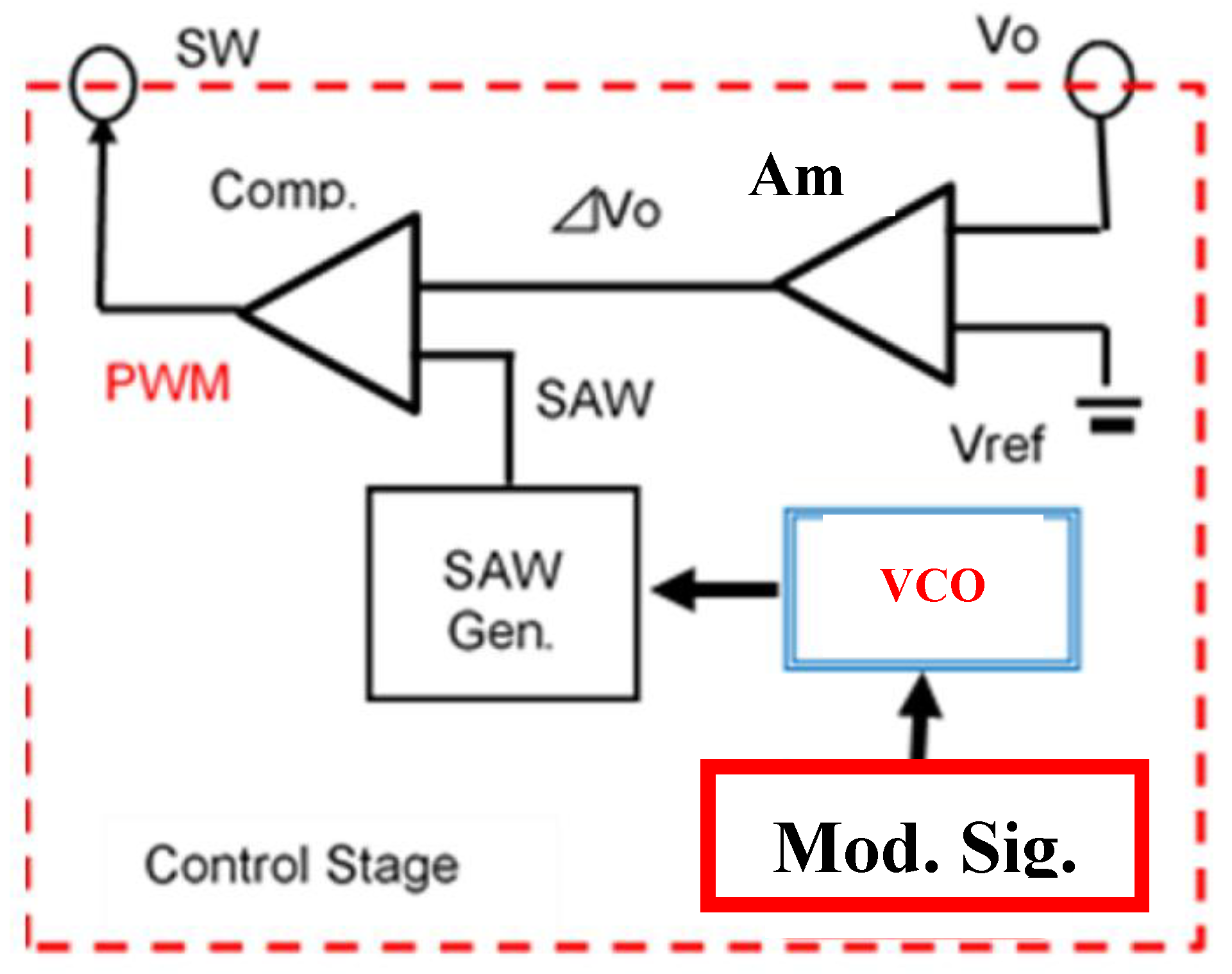
Figure 6.
Signals for frequency modulation.
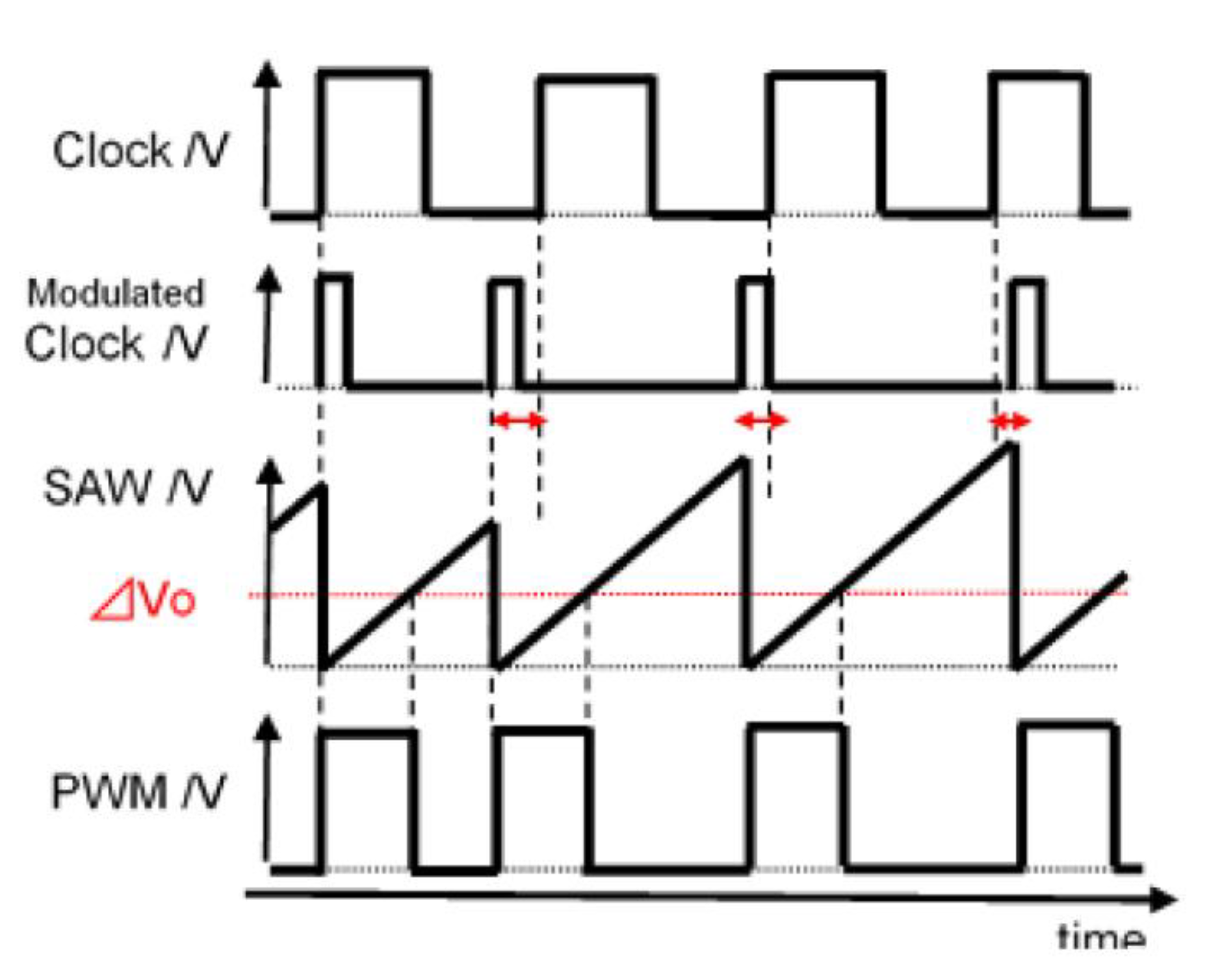
Figure 7.
Spread spectrum of PWM pulse [24] @JTSS.
Figure 7.
Spread spectrum of PWM pulse [24] @JTSS.
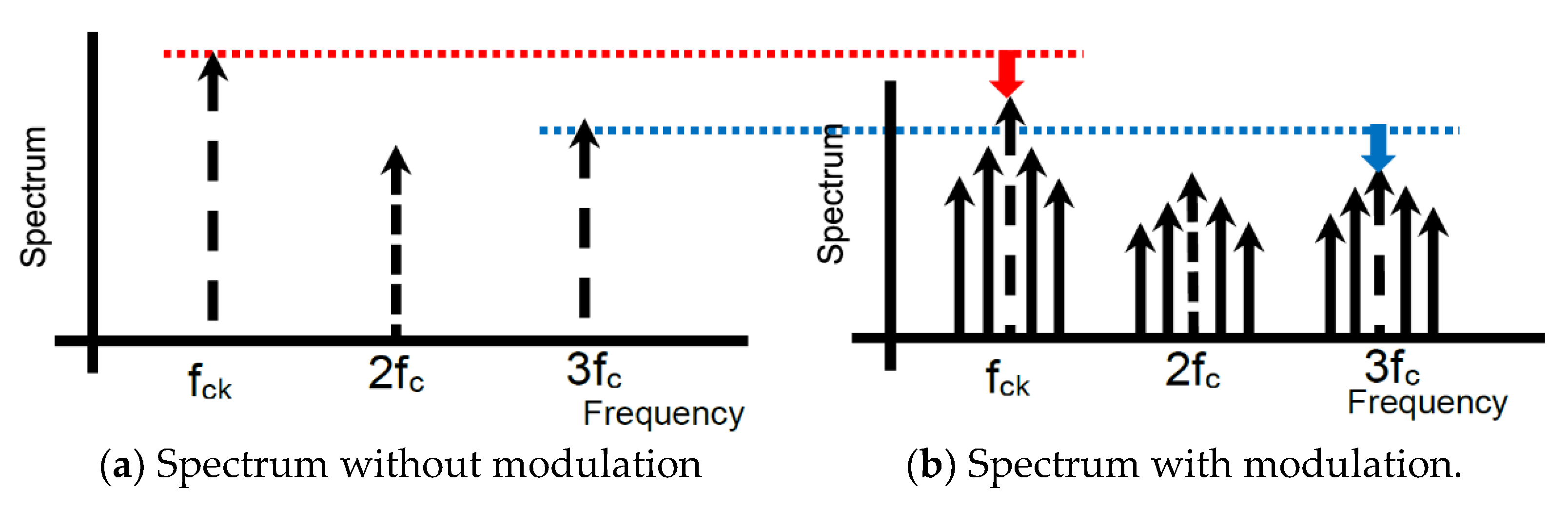
Figure 8.
PWM spectrum without clock modulation.
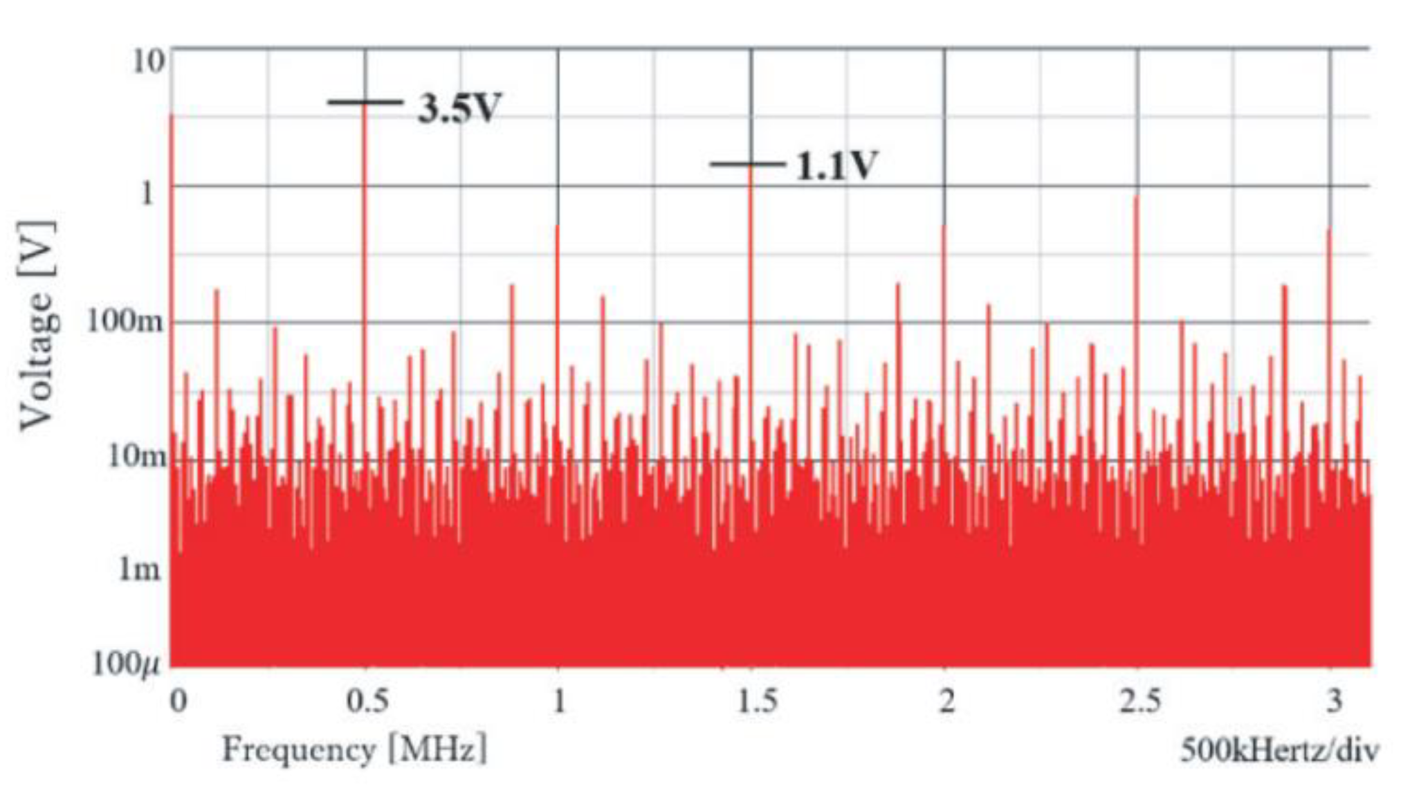
Figure 9.
PWM spectrum with modulation.
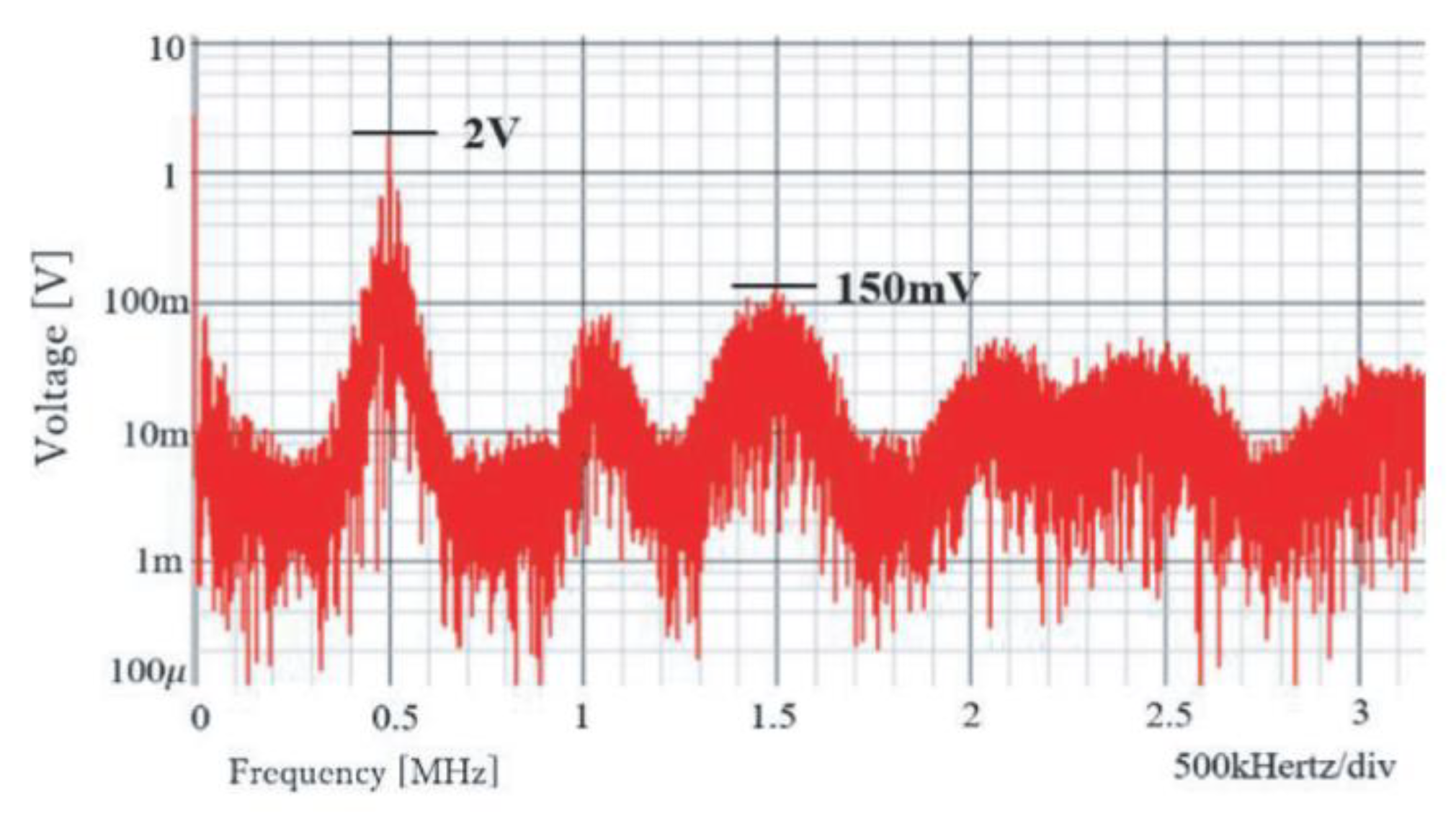
Figure 20.
Pattern generator using bit-inverse and bit-exchange [24] @JTSS.
Figure 20.
Pattern generator using bit-inverse and bit-exchange [24] @JTSS.

Figure 21.
Expanded pattern length with bit-inverse and bit-exchange [24] @JTSS.
Figure 21.
Expanded pattern length with bit-inverse and bit-exchange [24] @JTSS.
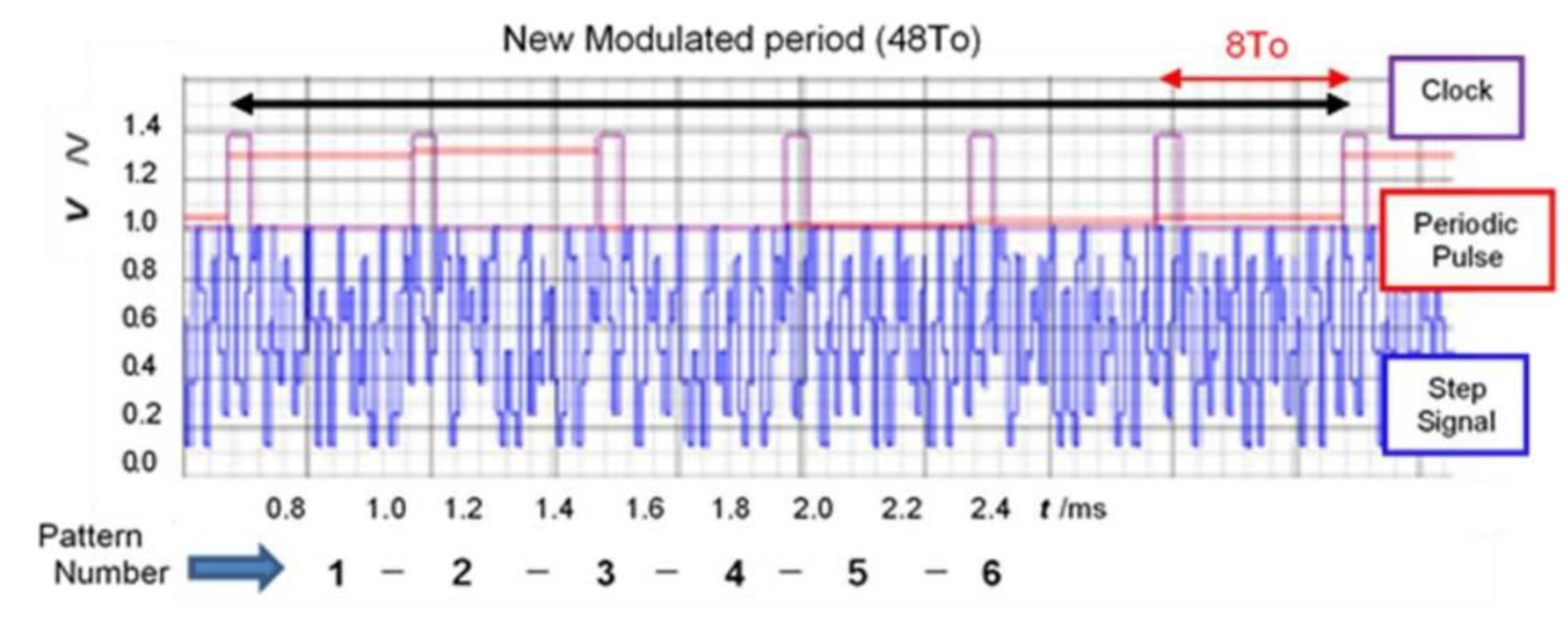
Figure 22.
Spectrum with bit-inverse and bit-exchange [24] @JTSS.
Figure 22.
Spectrum with bit-inverse and bit-exchange [24] @JTSS.
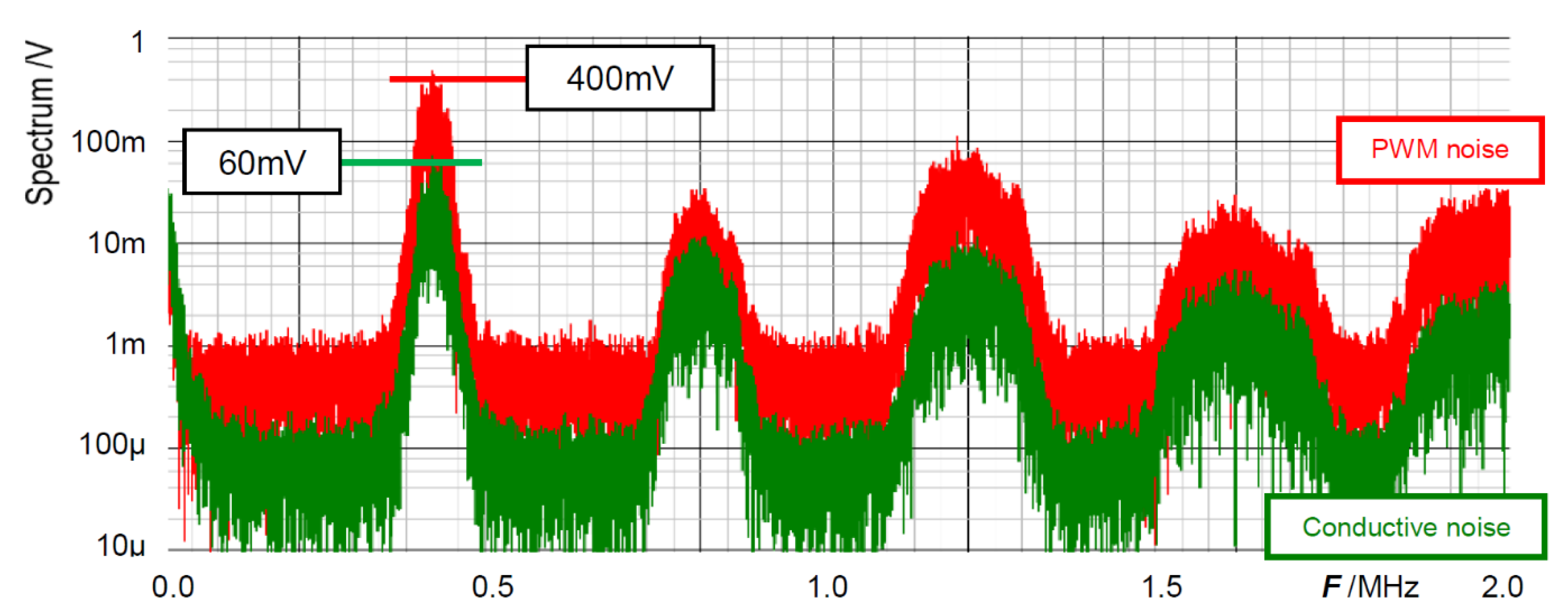
Figure 25.
Switching converter with basic pulse coding control [25] @IEEE.
Figure 25.
Switching converter with basic pulse coding control [25] @IEEE.
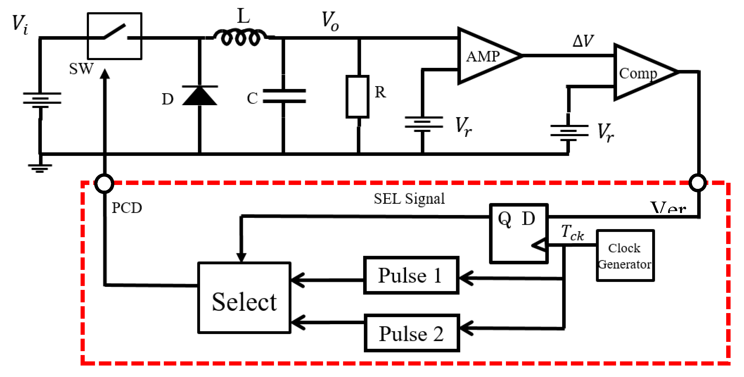
Figure 28.
Signals of PWC control.
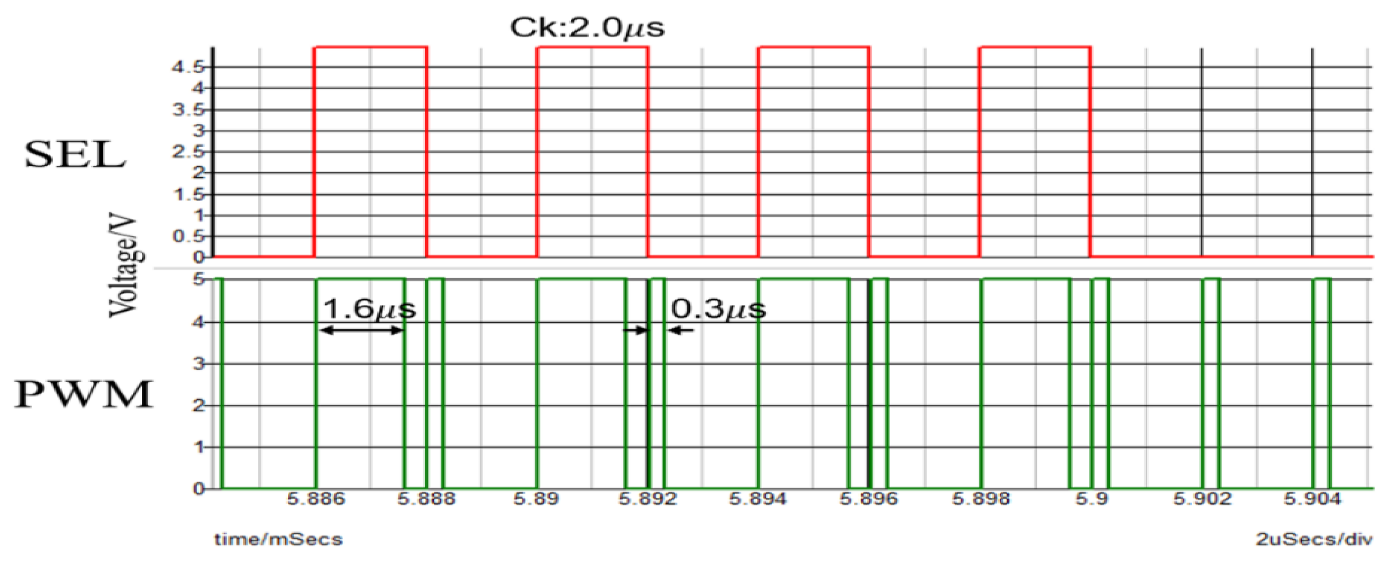
Figure 29.
Spread spectrum of PCD signal with PWC control.
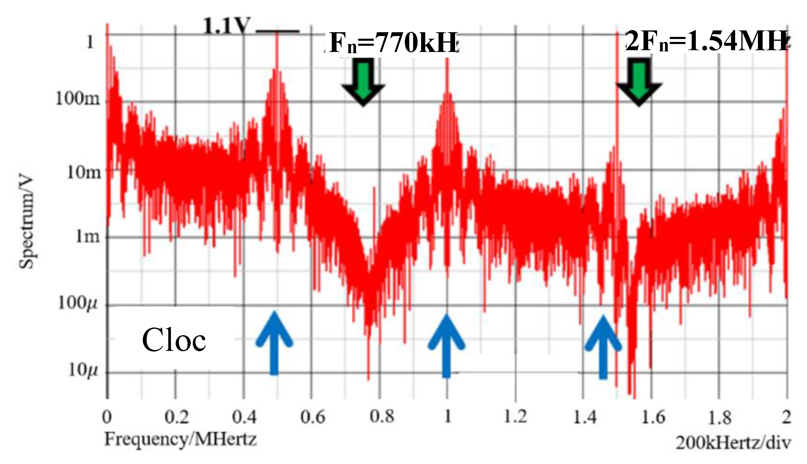
Figure 35.
Simulated signals of PCC method.
Figure 36.
Spread spectrum of PCD signal with PCC control (without spread spectrum).
Figure 37.
PWPC control circuit.
Figure 38.
Signals of PWPC control.
Figure 39.
Spread spectrum of PCD signal with PWPC control.
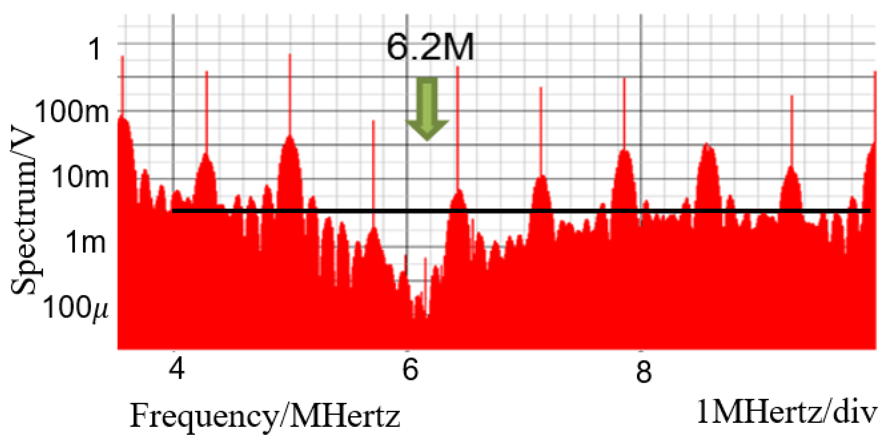
Figure 40.
One-period two-pulse train of PWC signal.
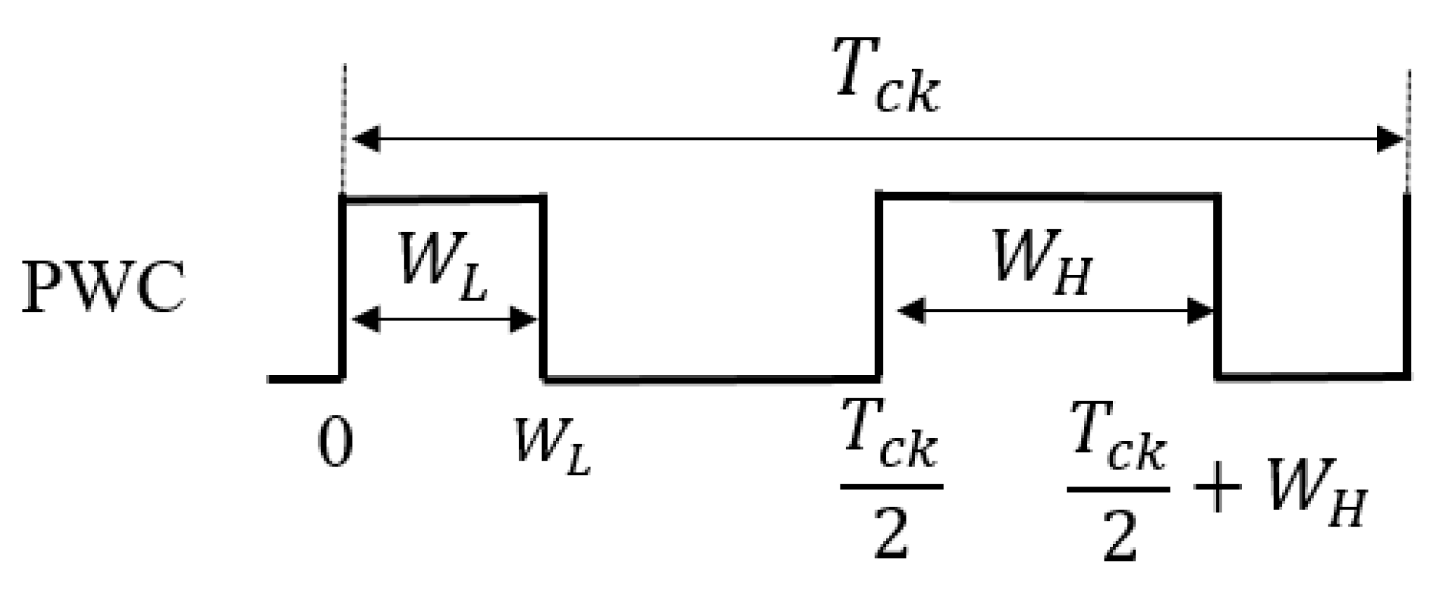
Figure 41.
One-period eight-pulse train of PWC signal.

Figure 42.
Comparison of theory and simulation.
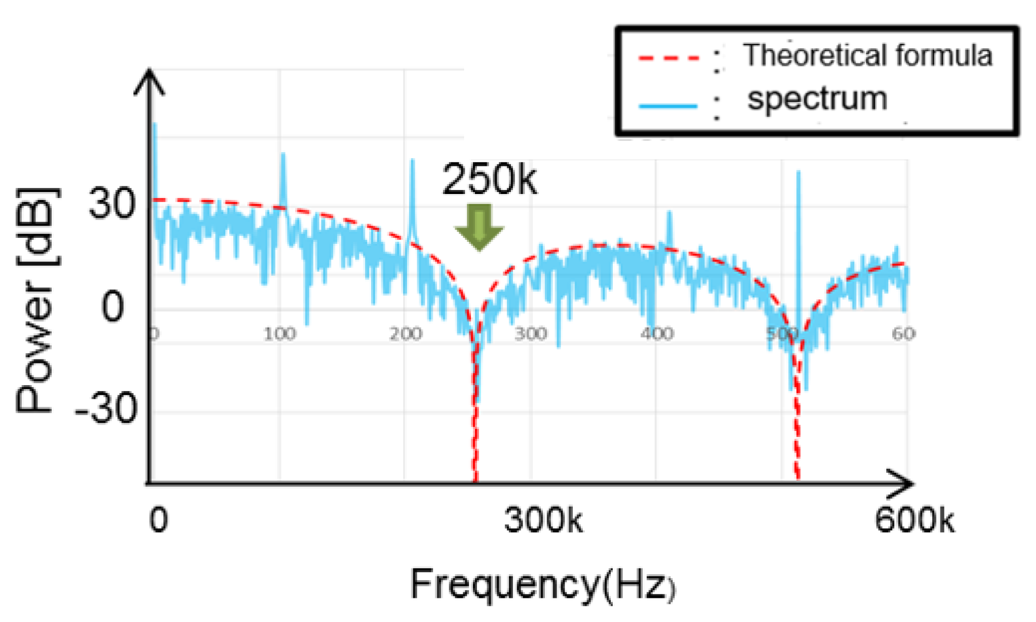
Figure 43.
One-period two-pulse trains of PPC signal.
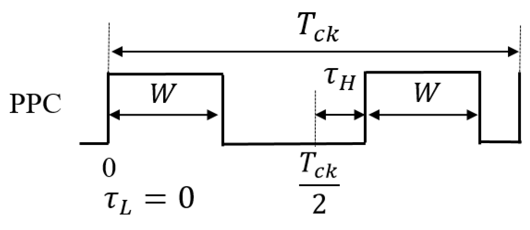
Figure 44.
One-period two-pulse train of PCC signal.
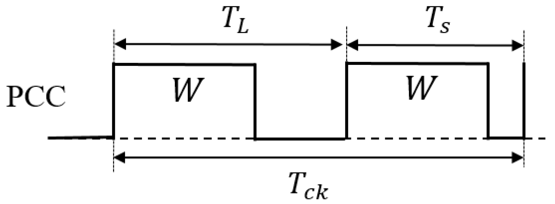
Figure 45.
One-period four-pulse-train of PWPC signal.
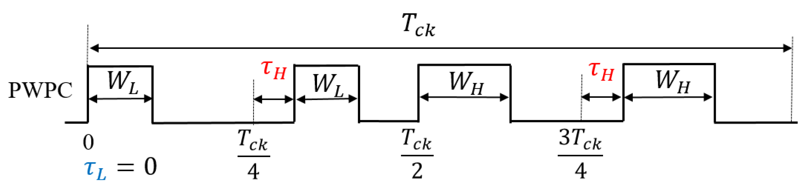
Figure 46.
Comparison of notch characteristics with PWC and PWPC methods.
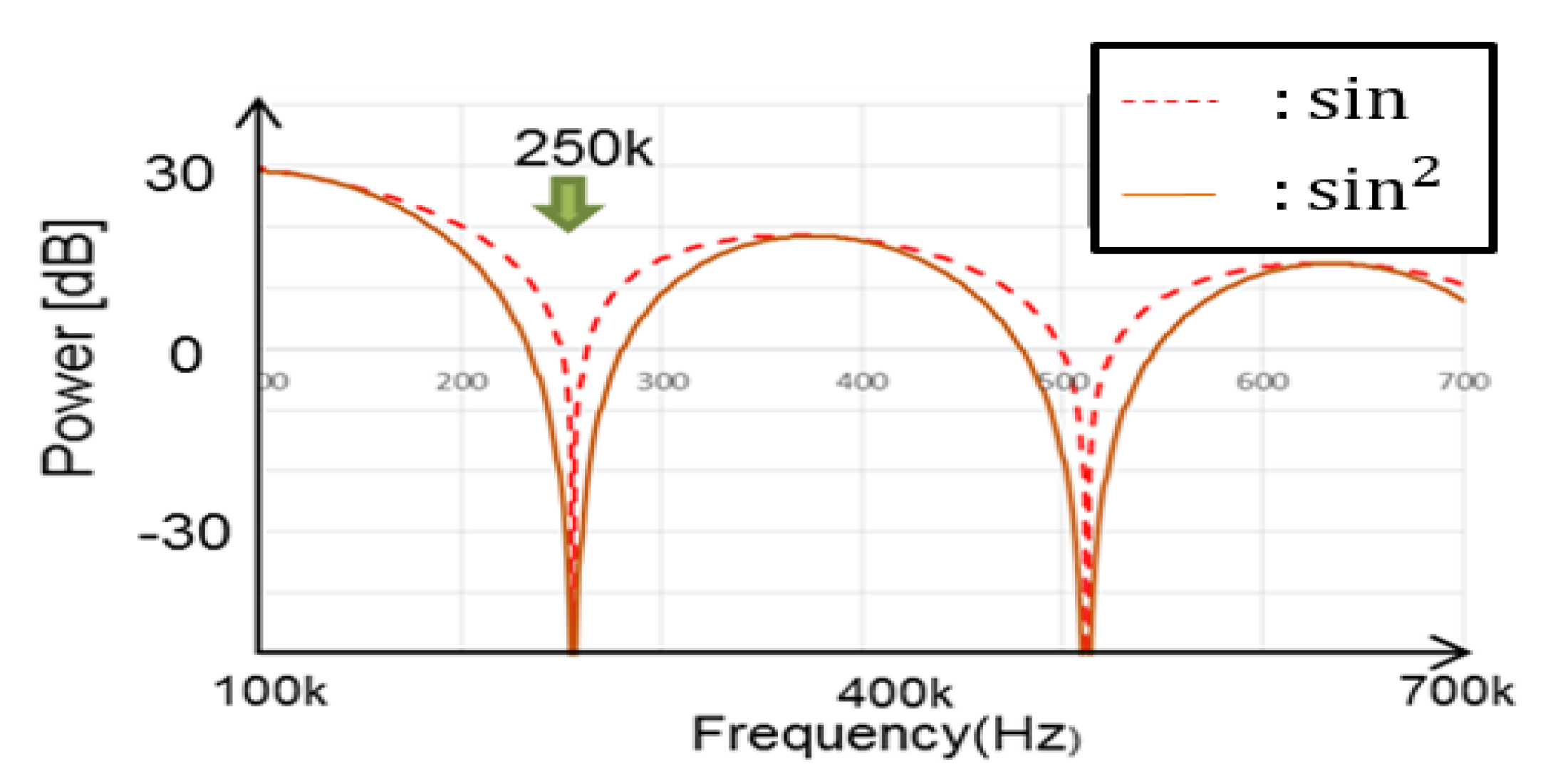
Figure 48.
Timing of Pulse-H and Pulse-L [26] @IEEE.
Figure 48.
Timing of Pulse-H and Pulse-L [26] @IEEE.
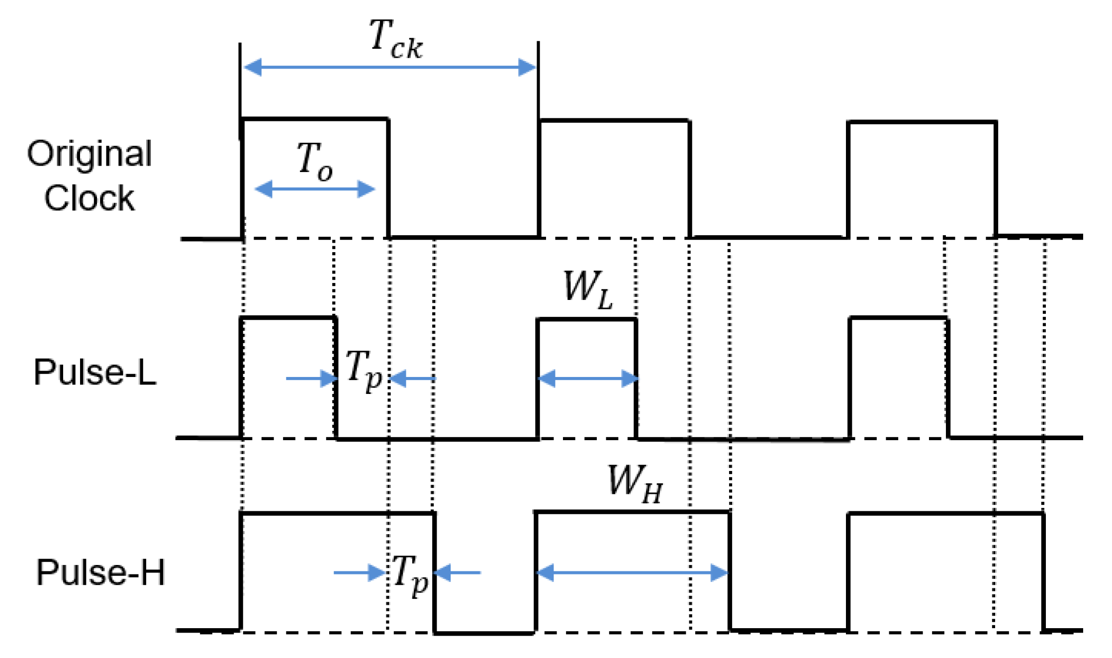
Figure 49.
Pulse coding circuit of automatic PWC method for [26] @IEEE.
Figure 49.
Pulse coding circuit of automatic PWC method for [26] @IEEE.

Figure 50.
Pulse coding circuit of automatic PWC method for .
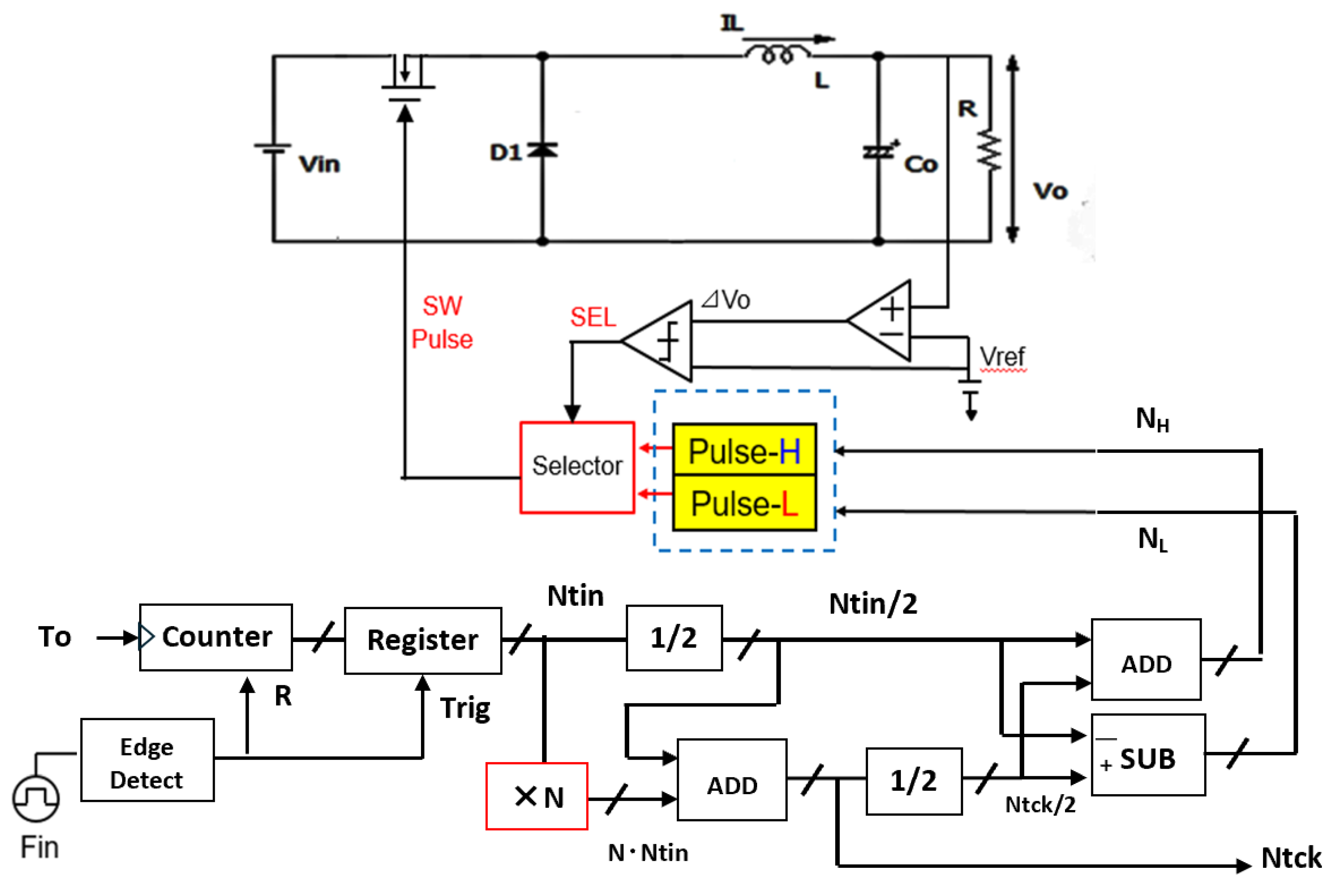
Figure 54.
Simulated waveforms for .
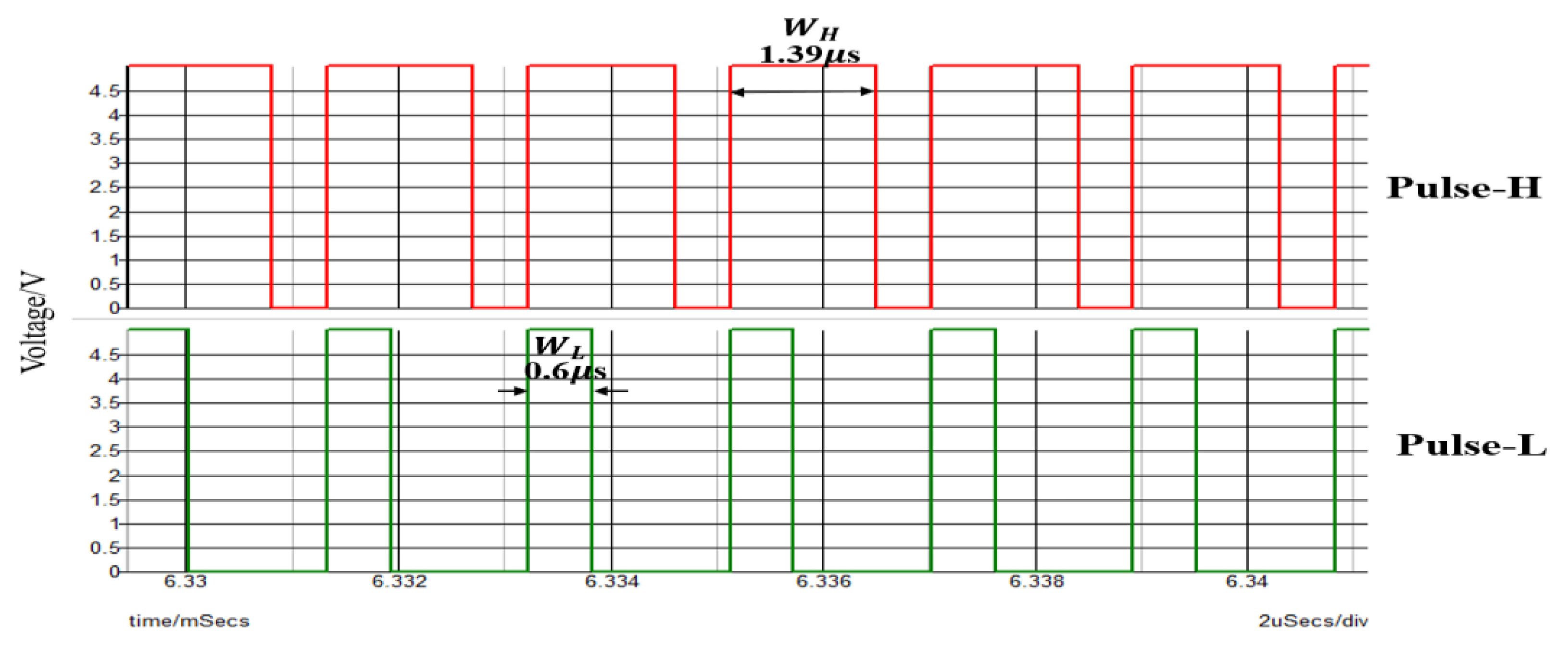
Figure 55.
Simulated spectrum with spread spectrum for .
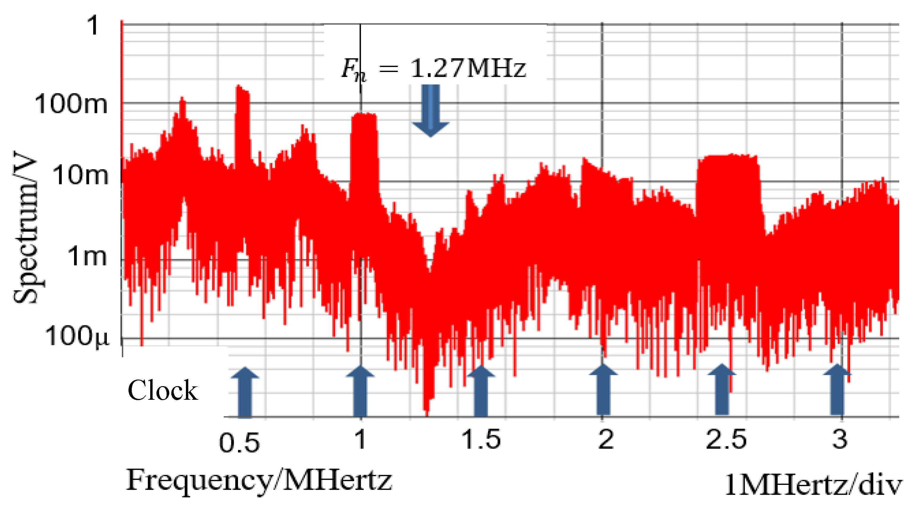
Figure 56.
Simulated waveforms for .
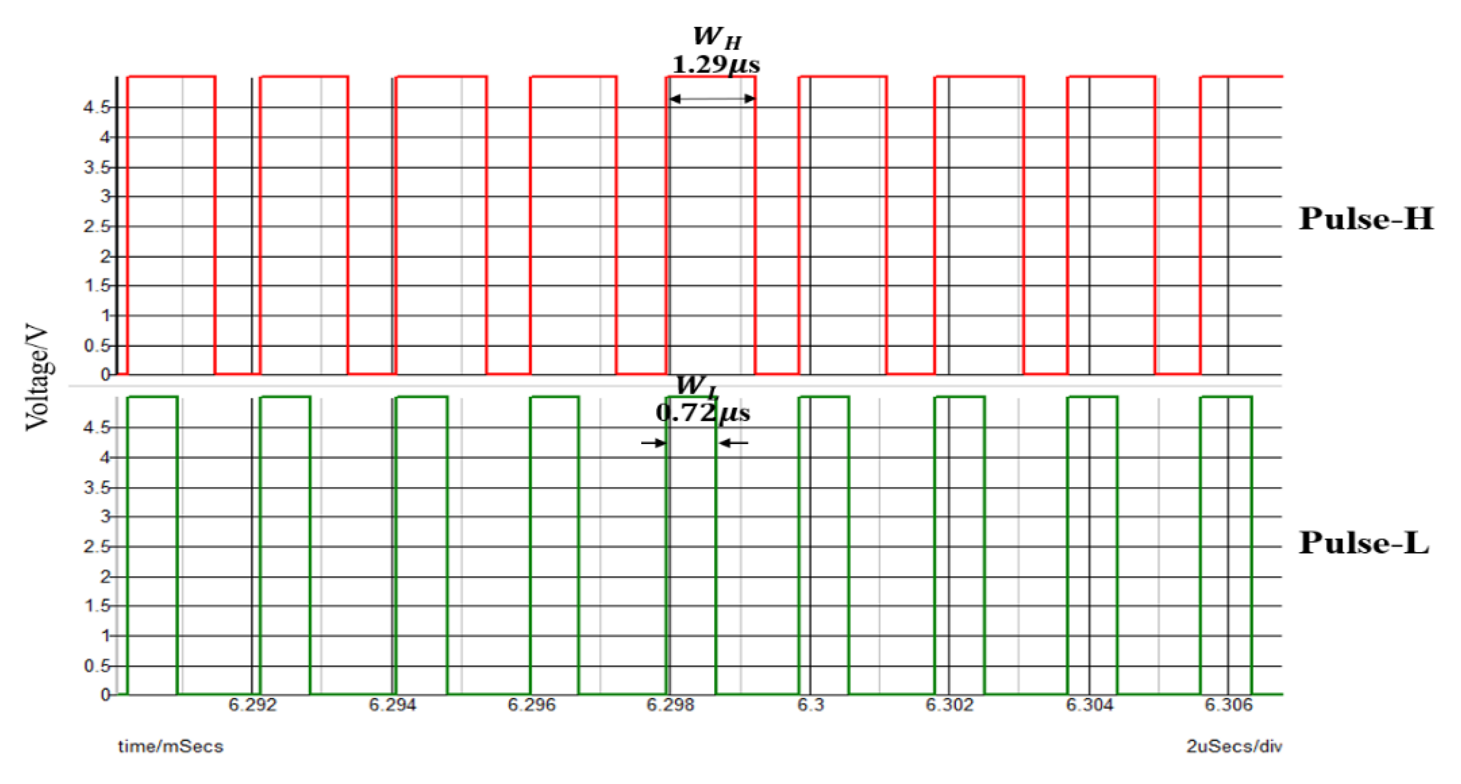
Figure 57.
Simulated spectrum with spread spectrum for .
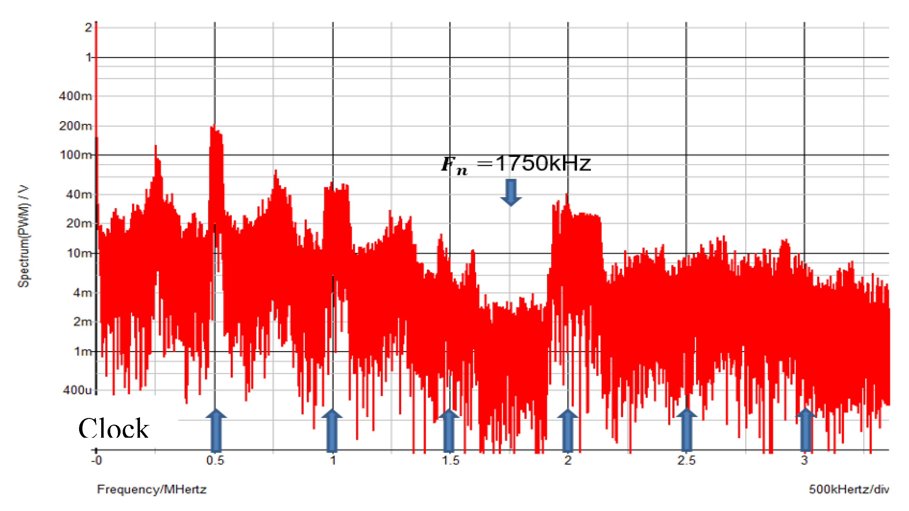
Figure 58.
Block diagram of change from channel 1 to channel 2.
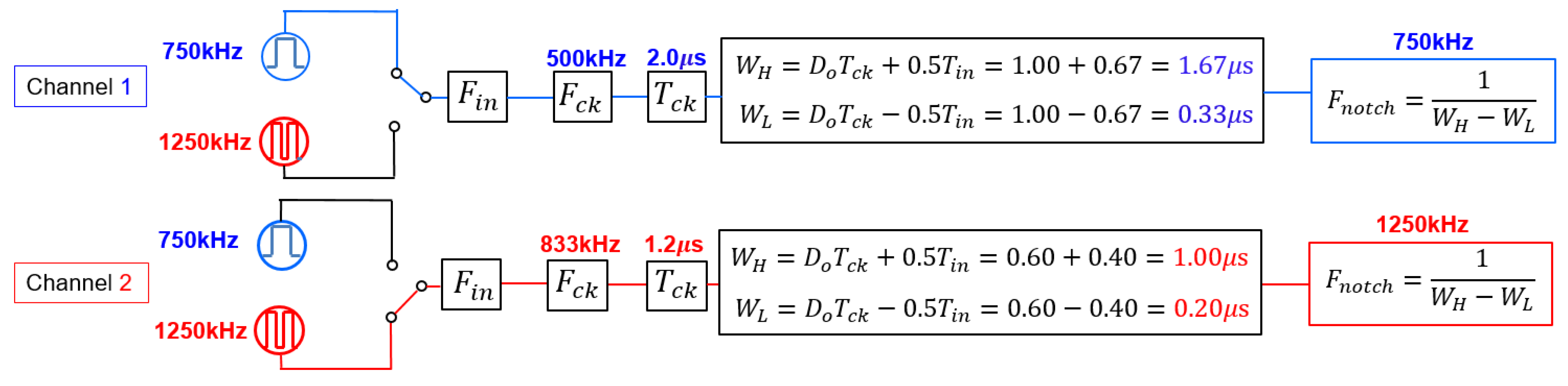
Figure 59.
Simulated spectrum for.
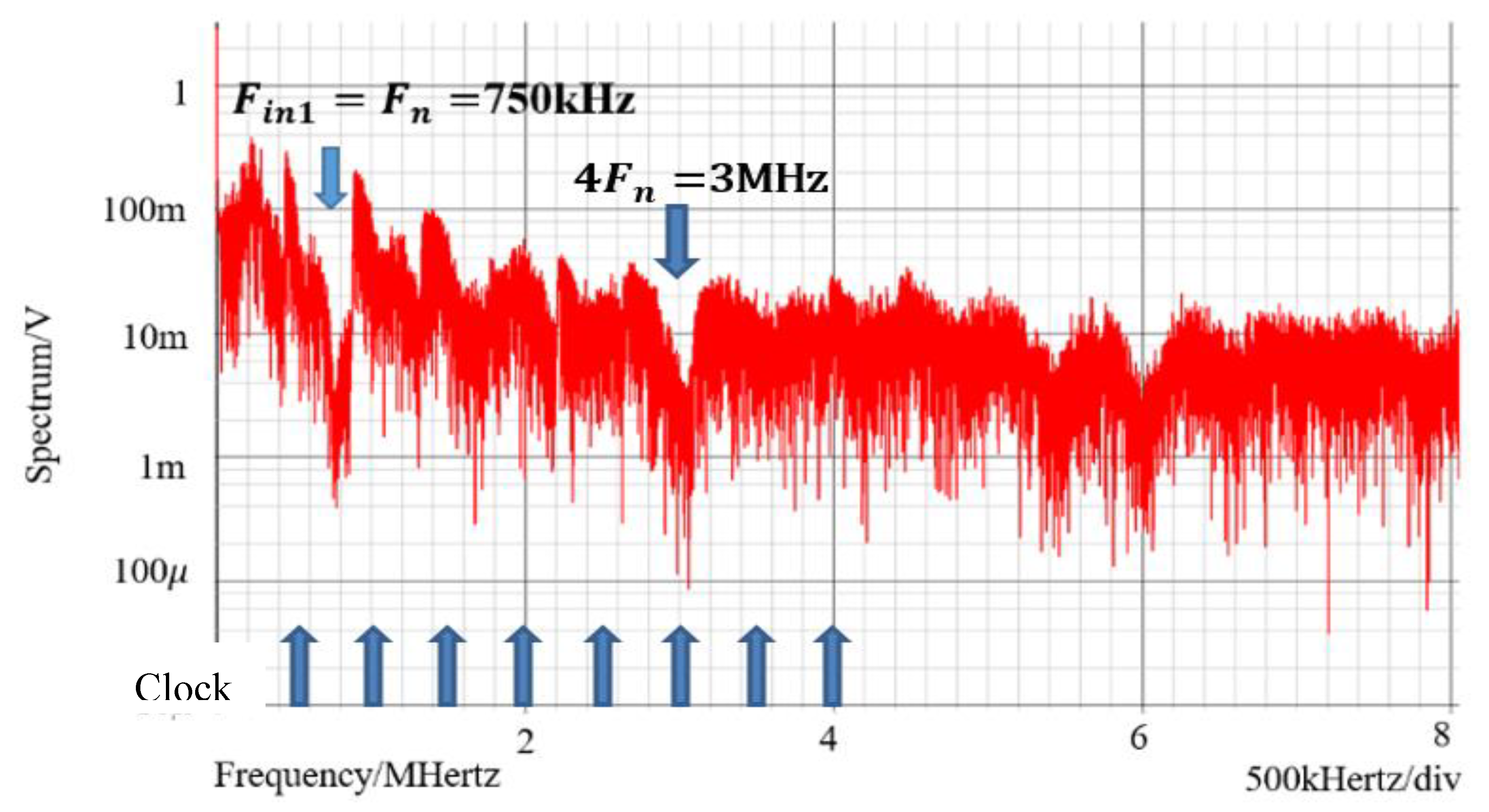
Figure 60.
Simulated spectrum for
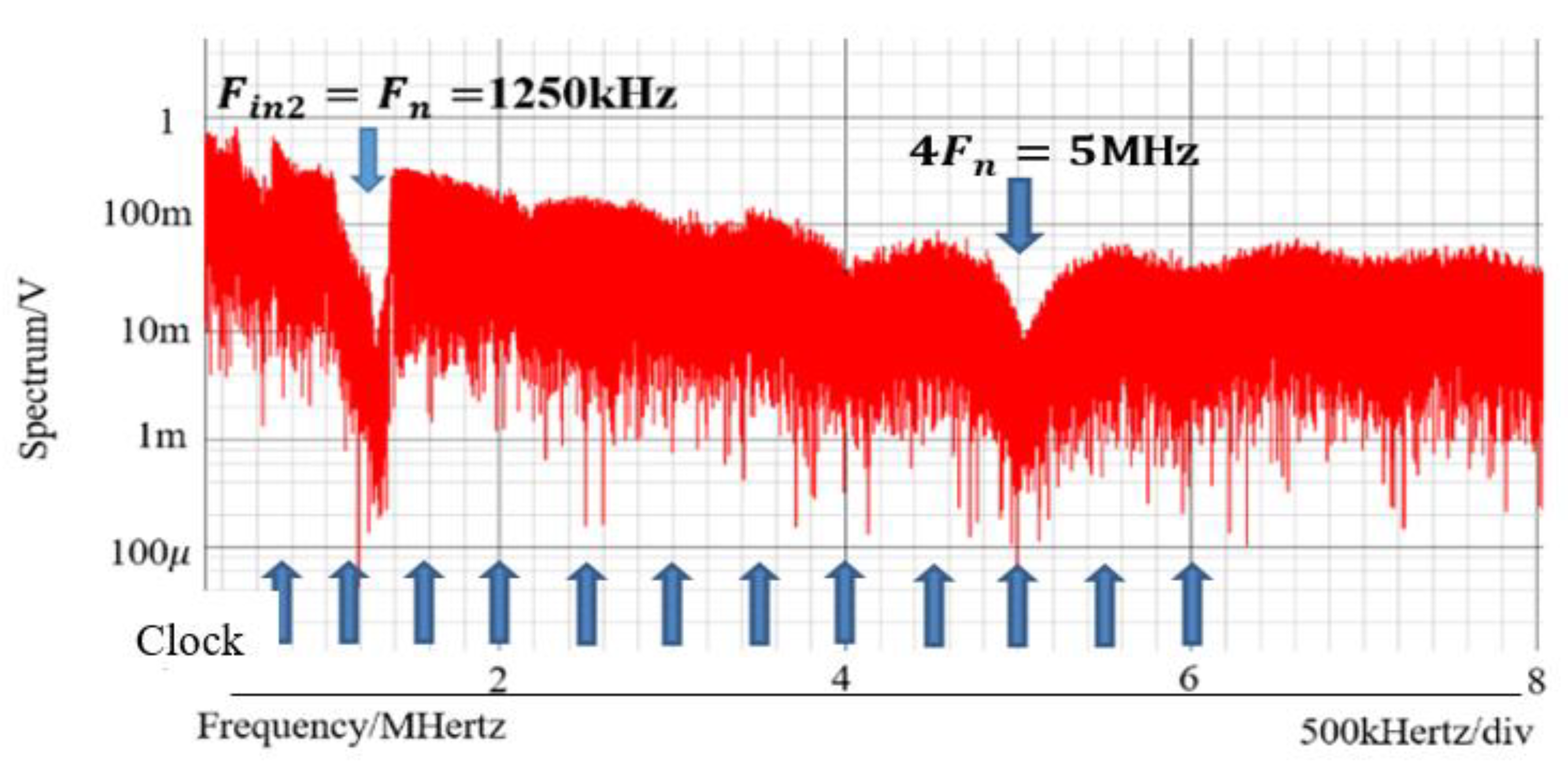
Figure 66.
Waveforms of SEL [27] @IEICE.
Figure 66.
Waveforms of SEL [27] @IEICE.
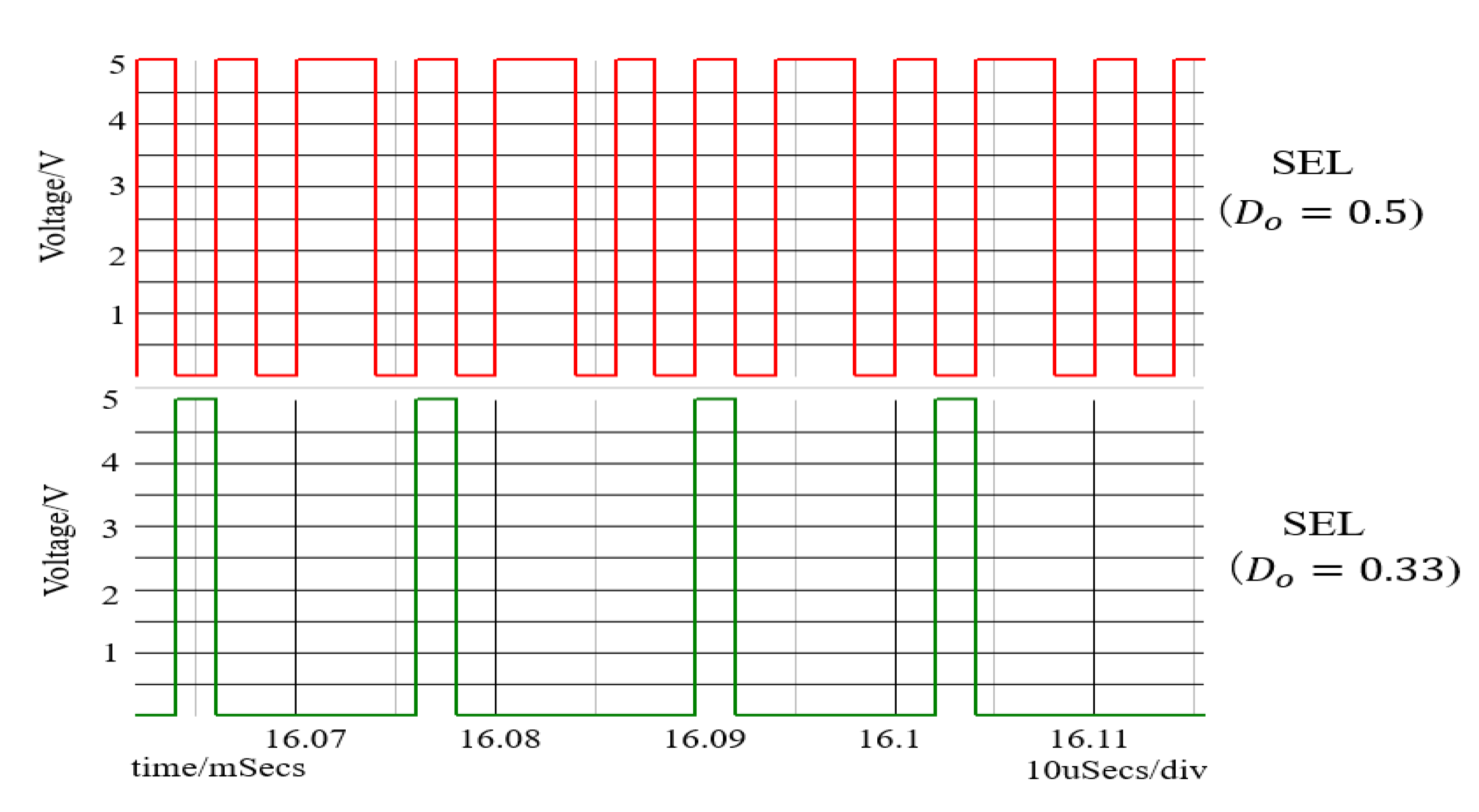
Figure 67.
Output voltage ripples [26] @IEEE.
Figure 67.
Output voltage ripples [26] @IEEE.
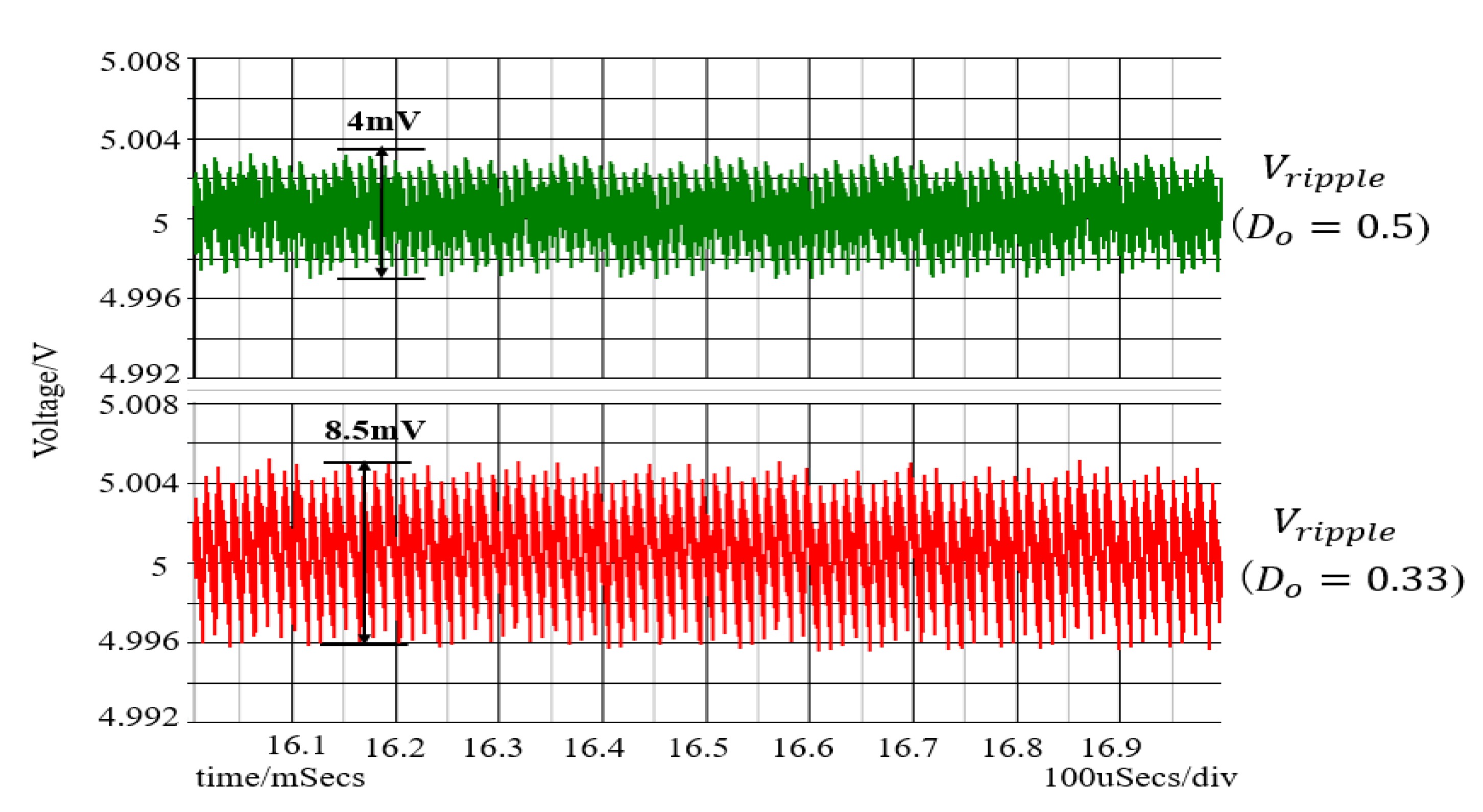
Figure 70.
Simulated spectrum with automatic generation without spread spectrum.
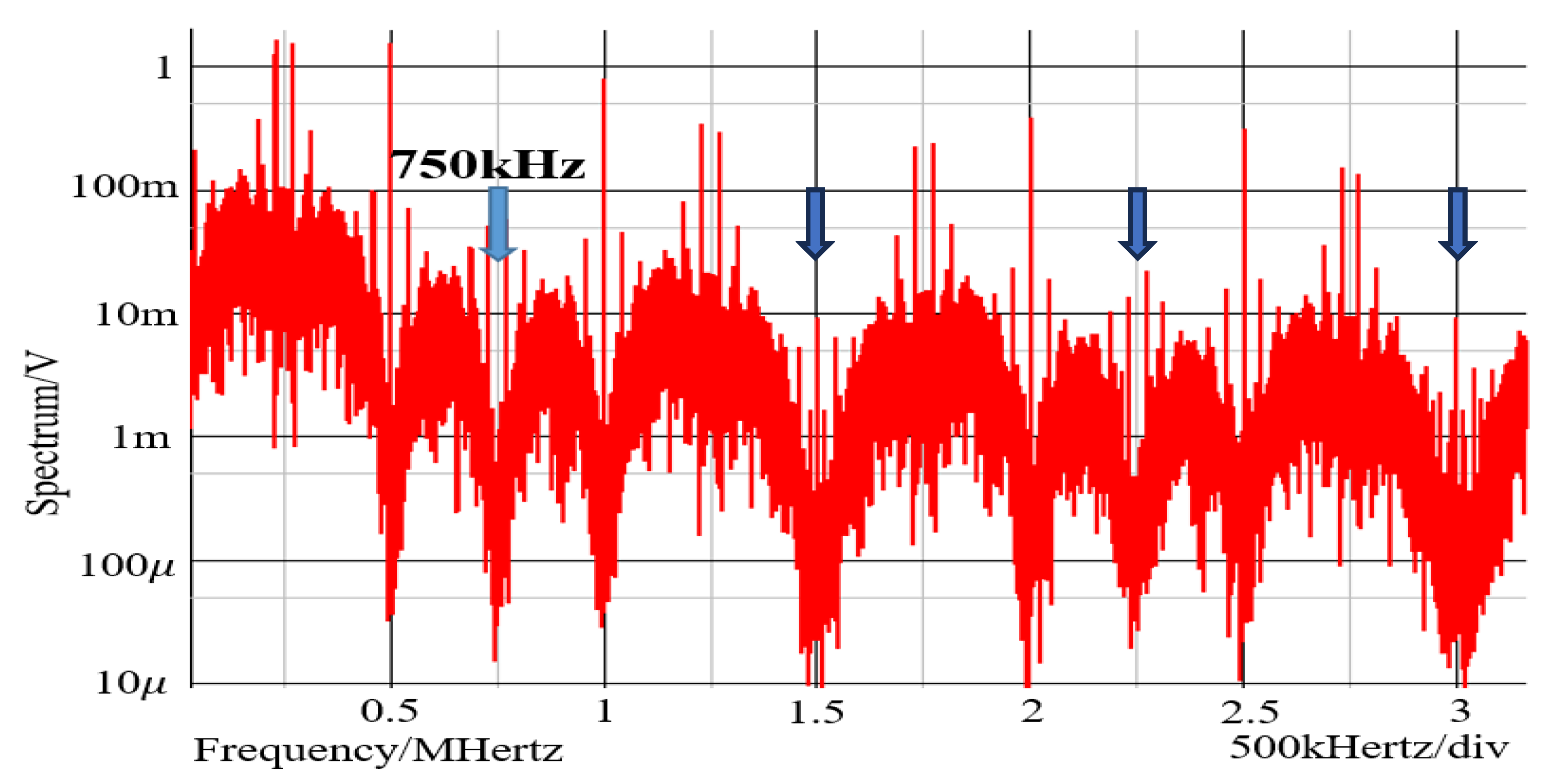
Figure 71.
SEL for automatic notch generation.
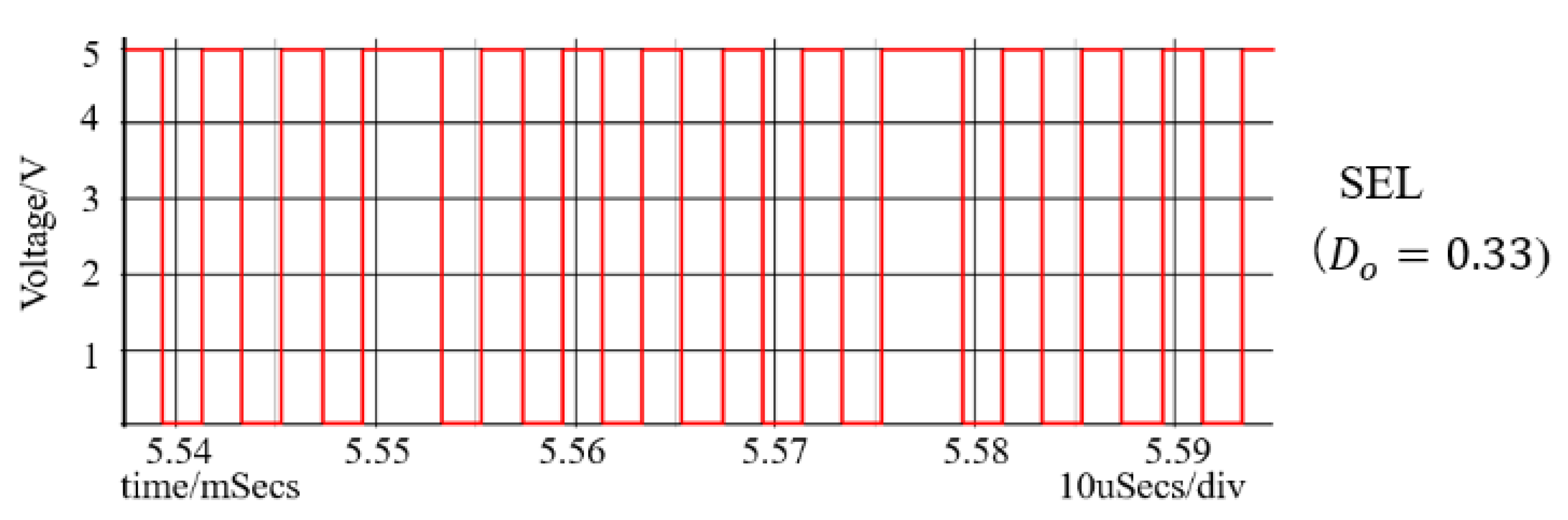
Figure 72.
Output voltage ripple in automatic notch generation.
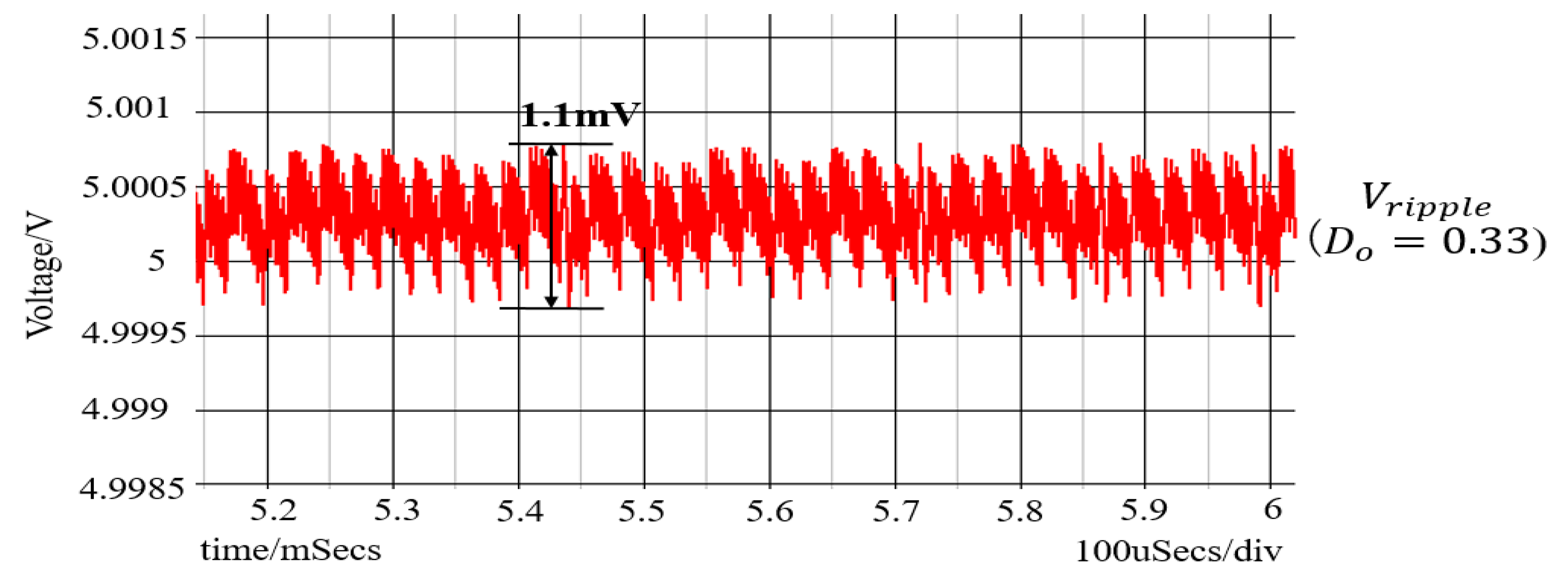
Figure 73.
Buck converter with PWC control.
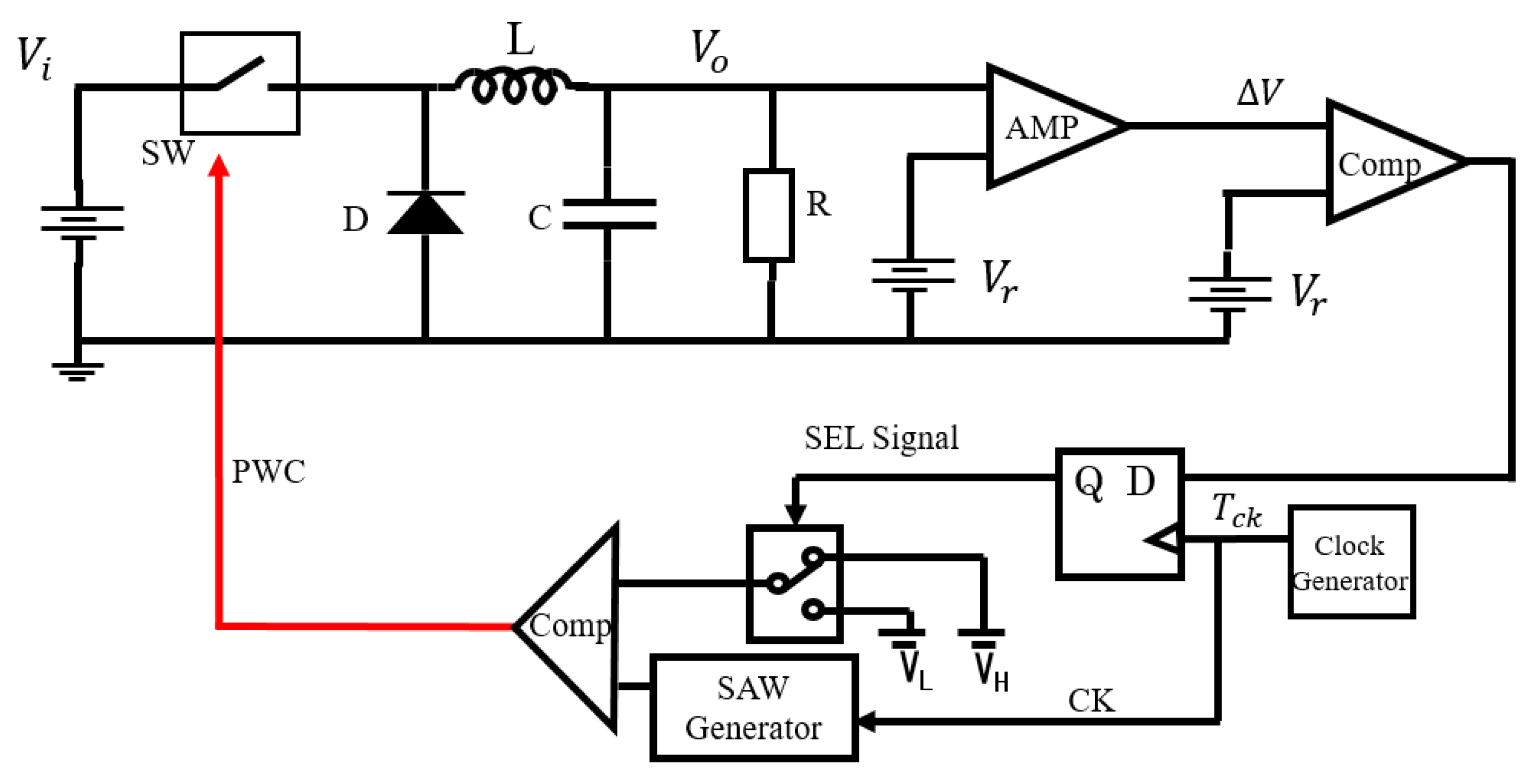
Figure 74.
Prototype of PWC control buck converter.
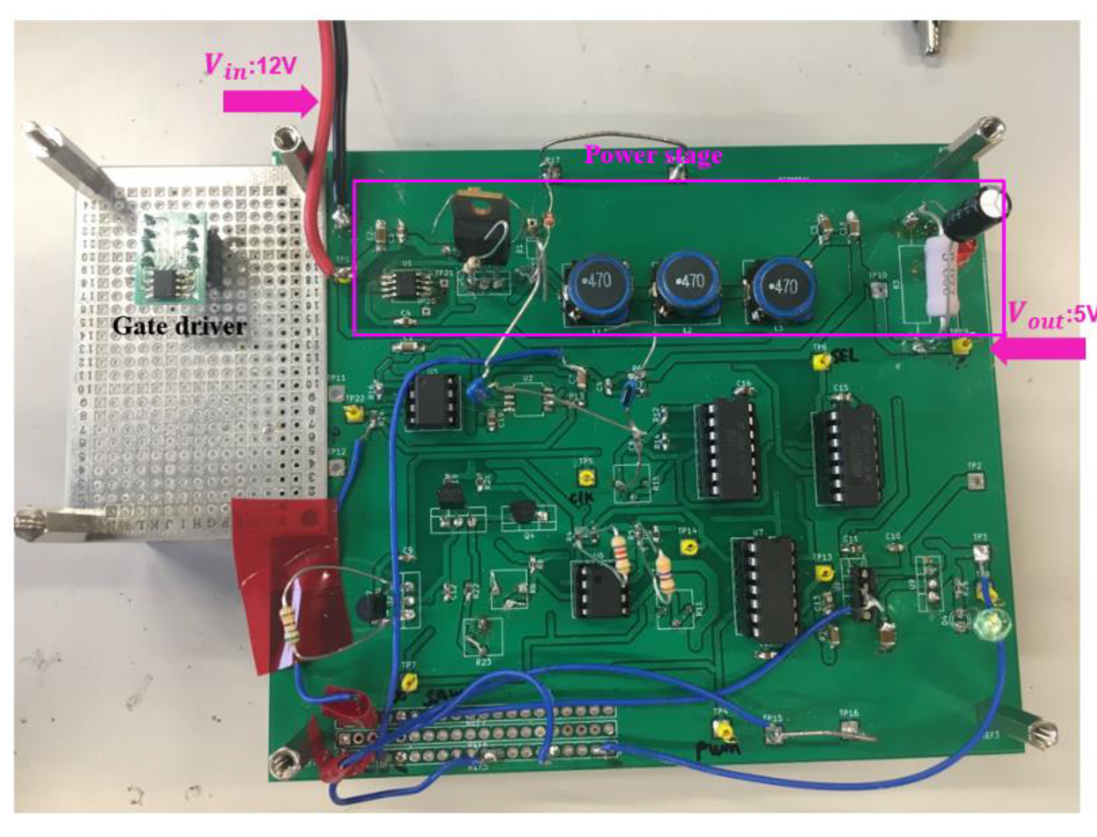
Figure 75.
Measured waveforms of and in the PWC control converter.
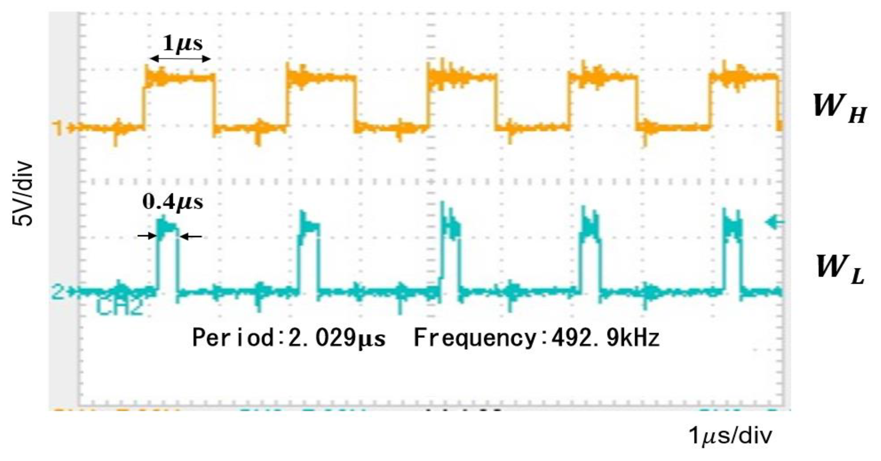
Figure 76.
Measured spectrum of the PWC control converter.
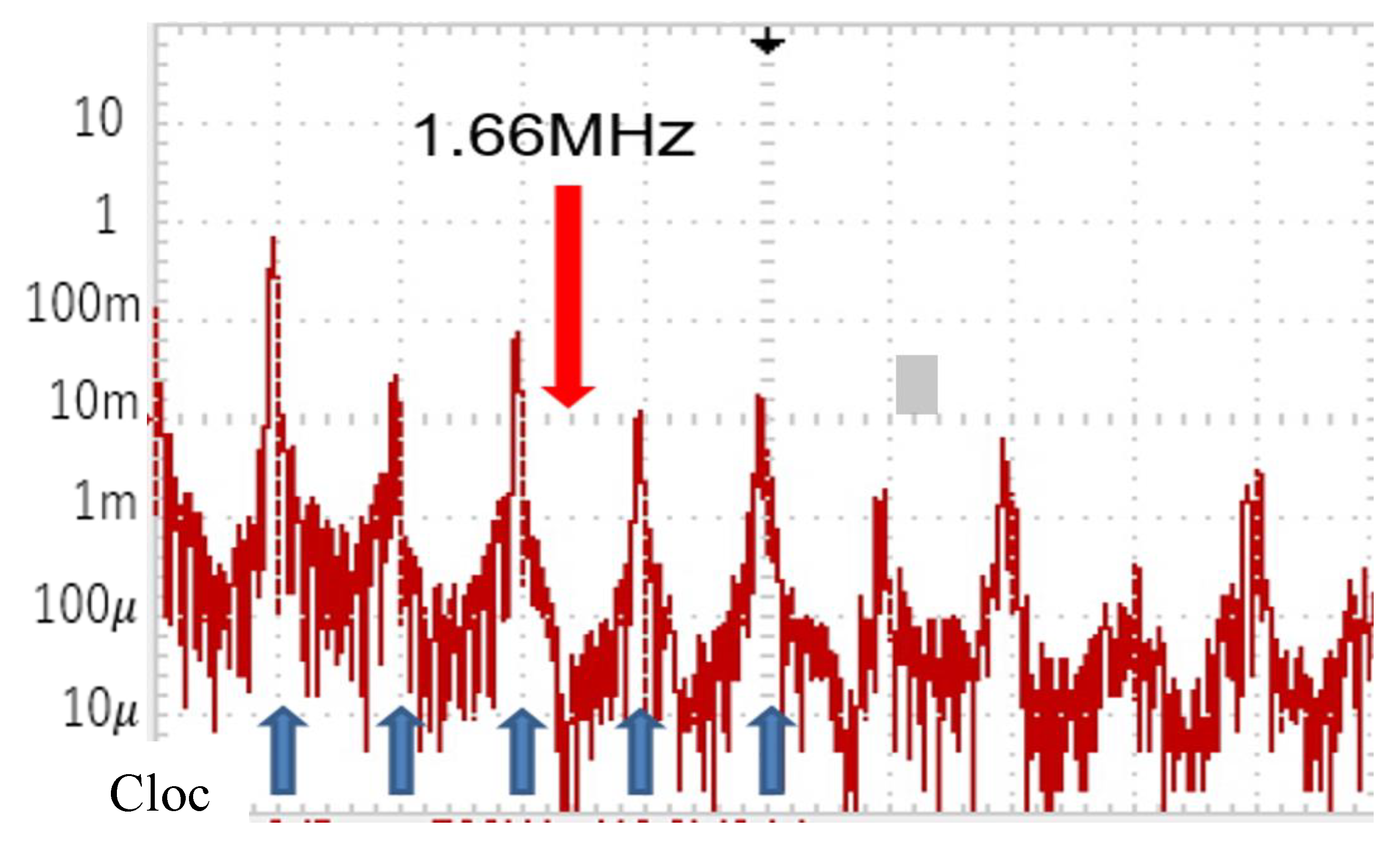
Figure 81.
Measured waveforms ().
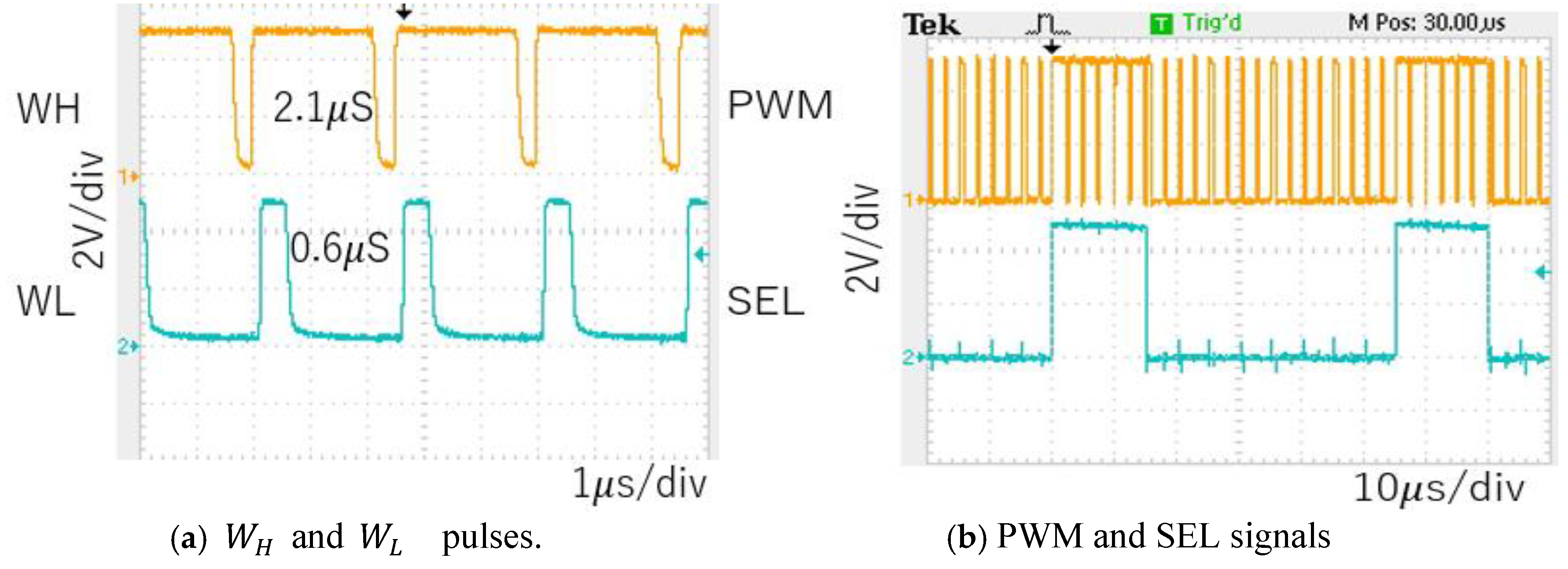
Figure 82.
Measured spectrum of PWM signal ().
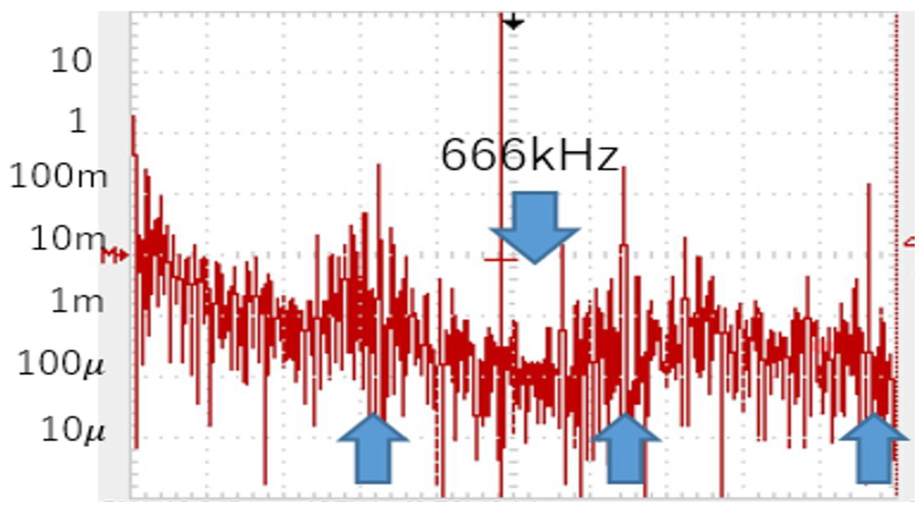
Table 2.
Parameters of PWC control simulation.
| 12V | 5V | 0.52A | 200 |
| 470 | 2.0s | 1.6s | 0.3s |
Table 3.
Parameters of PCC control circuit.
| 10V | 3V | 0.5A | 100 |
| 470 | 170ns | 600ns | 220ns |
Table 4.
Parameter values of Figure 73.
Table 4.
Parameter values of Figure 73.
| 12V | 5V | 0.2A |
| 100 | 47 | 500kHz |
Table 5.
Parameters of prototype.
| 10V | 3.5V | 0.16A |
| 141 | 570 |
Disclaimer/Publisher’s Note: The statements, opinions and data contained in all publications are solely those of the individual author(s) and contributor(s) and not of MDPI and/or the editor(s). MDPI and/or the editor(s) disclaim responsibility for any injury to people or property resulting from any ideas, methods, instructions or products referred to in the content. |
© 2025 by the authors. Licensee MDPI, Basel, Switzerland. This article is an open access article distributed under the terms and conditions of the Creative Commons Attribution (CC BY) license (https://creativecommons.org/licenses/by/4.0/).
Copyright: This open access article is published under a Creative Commons CC BY 4.0 license, which permit the free download, distribution, and reuse, provided that the author and preprint are cited in any reuse.


