Submitted:
17 March 2025
Posted:
18 March 2025
You are already at the latest version
Abstract
Recently developed photonic integrated circuits (PICs) for wireless communications are reviewed. These PICs leverage hybrid integration technology, which combines InP active elements, silicon nitride (Si3N4) low-loss waveguides, high-efficient ther-mal-optical tunable polymer with micro-optical functions to achieve fully integrated systems. This approach incorporates photonic building blocks, such as tunable lasers, on-chip optical isolators, optical phased arrays (OPAs), modulators, semiconductor optical amplifiers (SOAs), PIN-photodiodes, and waveguide-based photoconductive antennas. Among the key innovations are the generation of phase-locked optical sig-nals for wireless carrier at 45 GHz through on-chip frequency comb generation and injection locking, as well as the photonic-enabled beam steering across 20° at 300 GHz by integrating polymer-based optical phased arrays with InP PIN-photodiode-based antenna arrays. These advancements result in compact form factors, reduced power consumption, and enhanced scalability, positioning PICs as an enabling technology for future high-speed wireless networks.
Keywords:
hybrid integration
; wireless transceivers
; high-speed wireless communication
; photonic integrated circuits
1. Introduction
The rapid growth of global data traffic, driven by emerging technologies such as 5G/6G networks, the Internet of Things (IoT), and artificial intelligence (AI), has created an unprecedented demand for high-speed, high-capacity wireless communication systems [1,2]. Traditional radio-frequency (RF) technologies, while widely deployed, face fundamental limitations in bandwidth, energy efficiency, and signal integrity, particularly as we approach the millimeter-wave (mmWave) terahertz (THz) regime [3,4,5]. In this context, photonic technologies offer significant advantages [6]. By leveraging the ultra-wide bandwidth capabilities of mature optical fiber communication technology, photonic systems enable the generation and modulation of signals in the optical domain, which can be efficiently converted into the electrical signal up to THz range through photomixing [7,8,9].
Early demonstrations of photonic wireless systems relied on discrete components, such as fiber-coupled lasers, external Mach-Zehnder modulators (MZMs), and free-space optical setups. They achieved impressive data rates, for example, up to 100 Gbit/s in the 100 GHz band [10], but were limited by their large footprint, high power consumption, and susceptibility to alignment issues [4,5].
Recent advancements in photonic integration have enabled the development of chip-scale systems. Here, silicon photonics (SiPh) has gained significant attention due to its compatibility with CMOS processes, which enables low-cost and high-volume production of integrated modulators and detectors [11,12]. However, it faces challenges such as the lack of efficient on-chip light sources, and the lack of volumes required for CMOS style processes. This limitation has spurred the development of hybrid integration strategies, combining silicon with III-V materials like indium phosphide (InP) to incorporate high-performance lasers and amplifiers [13,14].
On the other hand, InP excels in monolithic integration of active components, such as lasers, amplifiers, and high-speed modulators, making them highly suitable for compact and efficient photonic transceivers [15,16]. However, InP is limited in passive component performance and for that, low-loss materials like silicon nitride (Si3N4) [17,18] and polymer [19,20] are better suited. Si3N4 is renowned for its ultra-low optical loss [17]. Polymer material platform such as PolyBoard [19,21] offers low-loss waveguide and features versatile micro-optical bench which can integrate bulk optic functionalities onto the chip. Its various refractive index contract waveguide system enables seamless co-integration with other materials. Additionally, lithium niobate (LiNbO3) has gained attention for its exceptional electro-optic properties, enabling high-speed modulators with low power consumption [22,23,24,25]. Furthermore, plasmonics-enabled modulators have demonstrated ultra-high frequency responses, reaching the sub-terahertz range [26].
Fraunhofer HHI has been developing solutions that provide compact form factors, reduced power consumption, and enhanced scalability for such photonic integrated circuits (PICs). For example, using PolyBoard platform to integrate active components such as lasers, modulators, photodiodes, as well as nonlinear and nonreciprocal bulk optic functionalities through hybrid integration [27,28,29,30].
In this work, we present a new generation of PICs for wireless communications, involving the InP, Si3N4 and polymer material platforms. This integration scheme offers fully integrated PICs with building blocks such as tunable lasers, on-chip optical isolators, optical phased arrays, modulators, semiconductor optical amplifiers (SOAs), positive-intrinsic-negative photodiodes (PIN-PDs) and waveguide-integrated photoconductive antennas (PCA). The generation of low-phase-noise wireless carriers through the on-chip frequency comb generation and injection locking yields a photonic engine for microwave signal generation. Moreover, the combination of an optical phased array (OPA) and InP PIN-PD based antenna array yields a directional and reconfigurable antenna array for the wireless communication.
2. Key Photonic Subsystems for Wireless Transceiver PICs
Hybrid integration takes the approach of using the advantage of each material platform. Table 1 lists the photonic functionalities offered on the material platforms that are going to be considered in this work for the implementation of the photonic wireless transceivers. The hybrid approach allows for good yield management even for complex photonic integrated circuits, as only known good dies from each platform are used for the hybrid integration. The key photonic subsystems which are going to be discussed are listed below:
- Optical injection-locked laser source for wireless communications
- Photonic THz emitter and receiver
- Beam steering with optical phased array (OPA) and optical beam forming network (OBFN)
2.1. Optical Injection-Locked Laser Source for Wireless communications
Figure 1 illustrates the schematic for generating phase-locked optical signals, a critical step in generating a low-phase-noise mmWave and THz signal by means of photomixing [9]. This process employs the optical injection locking technique [31,32], which ensures the phase coherence and stability in the generated signals. The required photonic building blocks for this subsystem are discussed in detail below.
2.1.1. InP/Polymer Tunable Laser
Hybrid PIC based external cavity diode lasers (ECDLs) have emerged as reliable, tunable, narrow linewidth laser sources. PICs with Vernier microring resonators (MRR) [33], distributed Bragg reflectors [34,35,36], Sagnac loop reflectors (SLRs) [37], and Mach-Zehnder interferometers [38] have been fabricated on silicon (Si) [38], silicon dioxide (SiO2) [39], silicon nitride (Si3N4) [33,34,35,40,41], polymer [36,42], and other materials [43].
Fraunhofer HHI’s PolyBoard and InP foundry platforms offers the hybrid InP/polymer tunable distributed Bragg reflector (DBR) lasers, operating in the telecom window with a center wavelength of approximately 1550 nm. These lasers offer a tuning range exceeding 20 nm, a narrow linewidth of 185 kHz, and optical power levels of up to 40 mW [42]. One of these lasers serves as the master laser, which generates the optical carrier fed into the InP phase modulators. Its wide tunability and high stability makes it ideal for generating precise optical carriers required for low-phase-noise signal generation.
The characterization of hybrid DBR lasers in a master-slave configuration has been experimentally verified to achieve stable injection locking. By defining the detuning frequency Δf as the difference frequency between the master laser and slave laser, and the internal injection ratio as the ratio of the injected power to the slave laser power, the locking behavior is charted in Figure 2. The locking range of 0.2 GHz to 3.8 GHz was observed. Under stable injection-locked conditions, the slave laser follows the frequency of the master laser, and the measured frequency difference is less than 20 MHz. The boundaries of the locking range are visible as sharp transitions. Outside the locking range, the frequency difference increases significantly. For a large internal injection ratio , a small unstable region is observed within the locking range, corresponding to the undamped relaxation oscillations [44]. In this region, the frequency deviation increases abruptly, as the relaxation oscillations dominate the power distribution and alter the optical frequency.
2.1.2. InP Electro-Optic Modulator
There are several different ways of generating optical frequency combs (OFCs) using integrated photonic approaches, e.g. Kerr soliton combs in high-Q microresonators [45,46], which offer ultra-low phase noise and broad bandwidth but require precise control of pump power and dispersion, mode-locked lasers [46,47], which provide excellent coherence and high repetition rates but have limited tunability due to fixed cavity designs, gain-switched laser combs [48], which are simple and cost-effective with moderate tunability but suffer from spectral flatness and phase noise limitations.
Here, we choose two cascaded InP-based electro-optic modulators which are modulated with sinusoidal RF driving currents and thus generate an optical frequency comb (OFC) [49,50,51]. This offers a highly flexible and frequency tunable approach, making them particularly suitable for microwave photonics applications. E/O combs can be precisely controlled via microwave driving signals, enabling tailored comb spacing and phase coherence, which are critical for generating high-quality microwave signals.
The InP foundry integration platform at HHI provides high-bandwidth traveling-wave modulators based on the quantum-confined Stark effect (QCSE) [51,52]. Additionally, SOAs can be integrated directly after the phase modulator to enhance the power of each comb line. Figure 3 (a) shows the InP chip with two cascaded phase modulators and followed by a SOA, and an example of generated OFC is shown in Figure 3 (b).
2.1.3. Optical Isolators
Optical isolators are essential in the injection locking technique to prevent feedback from the slave lasers, ensuring stable operation of the system. The PolyBoard platform’s micro-optical bench allows for the integration of bulk nonreciprocal optical elements directly into a photonic chip. The isolator incorporates a Faraday rotator sandwiched between a 0° polarization filter and a 45° polarization filter, followed by a 22.5° half-wave plate (HWP) to ensure TE polarization in forward transmission direction. The optical coupling between waveguide and free-space is optimized through gradient-index (GRIN) lenses, which can be placed in the etched U-groove structures on the PolyBoard. Figure 5 (a) shows a close-up picture of the integrated optical isolator. Over 30 dB isolation across C-band with an excess loss below 1.5 dB can be achieved as shown in Figure 5 (b) [29,30,53].
2.2. Photonic THz Emitter and Receiver
By superimposing the two phase-locked optical signals, a stable optical beat note is generated, which is then converted into a THz signal using a photomixer. On the receiver side, the beat note serves as local oscillator to down-convert the incident THz signal to an intermediate frequency for electronic acquisition. For the transmitter (Tx), commonly PIN-PDs or uni-traveling-carrier (UTC) PDs are employed as photomixer [54,55,56,57], while photoconductive antennas (PCAs) are better suited for the receiver (Rx) [58,59,60].
For our transmitter, waveguide-integrated PIN-PDs, based on mature processes originally developed for fiber-optic communication systems, have demonstrated coherent links with data rates of up to 160 Gbit/s and well-defined radiation patterns [61,62]. For coherent communication, an InP in-phase/quadrature (I/Q) modulator imprints the data onto one of the optical signals before superposition as shown in Figure 6. An I/Q modulator is typically constructed using two parallel Mach-Zehnder modulators (MZMs). All these building blocks, i.e. lasers, MZMs, and PDs are readily available on the InP platform.
On the receiver side, the antenna receives the incident THz signal, which results in a voltage variation with the frequency at the photoconductor in the feeding point of the antenna. At the same time, the optical beat signal fed into the photoconductor acts as a local oscillator (LO) with the difference frequency of the two phase-locked laser signals , which modulates the conductance of the photoconductor. This oscillating conductance in the feeding point of the antenna leads to a down-conversion of the THz signal to an intermediate frequency (IF) , that can be measured with conventional electronics. Note that photonic integration requires waveguide-integrated PCAs and not traditional top-illuminated designs [64]. By integrating the PCA with optical waveguides, evanescent coupling enhances the light coupling efficiency into the photoconductive material. Unlike top-illuminated PCAs, which suffer from reflections at the air-semiconductor interface, waveguide-integrated PCAs minimize these losses by coupling light from below, resulting in improved optical absorption and higher output signal strength. Recent developments in waveguide-integrated PCAs have demonstrated up to 22-fold improvement in photoresponse compared to state-of-the-art top-illuminated designs [64], enabling flexible integration of THz receivers into photonic integrated circuits.
2.2.1. Scaling-Up with Antenna Arrays
To address the limitations of emitted power [57,65] and antenna directivity [66,67] in mmWave and THz communication systems, arrays of antennas are implemented. The antenna pitch must be smaller than the targeting wavelength (λ) to achieve beam steering capability, necessitating waveguide-integrated designs to enable the required compact spacing, which discrete components cannot provide. This approach enables scalable and high-performance THz transmitter and receivers. A 1x4 THz emitter array based on PIN-PDs integrated with SOA [65] and a 1x4 THz receiver array based on PCAs are depicted in Figure 8 and Figure 9, respectively. Spot-size-converters (SSCs) are included on the chip facet to facilitate the coupling towards standard fiber array or other chip platforms.
2.3. Beam Steering with Optical Phased Array (OPA) and Optical Beam Forming Network (OBFN)
Beam steering can be achieved by integrating optical phased arrays (OPAs) with antenna arrays, where the phase of each individual antenna element is precisely controlled [68]. Figure 10 illustrates a schematic design of such an OPA, which utilizes two phase-locked optical signals as inputs. Power-splitting elements, such as multimode interferometers (MMIs) distribute the signals to the desired number of antennas. To maintain phase correlation between the two signals, the optical path lengths must be identical, necessitating low-loss waveguide routing. By introducing phase shifting in one of the optical signals, wide steering angle can be achieved with tuning speeds in the MHz and GHz range [67,69,70].
The PolyBoard platform offers waveguide propagation loss down to 0.8 dB/cm [19] and also includes building blocks such as efficient thermo-optical phase shifters with low crosstalk. These phase shifters leverage the platform's high thermo-optical coefficient and low thermal conductivity, outperforming other photonic integration platforms [65].
Figure 11 shows a packaged 1x4 OPA array based on the PolyBoard platform. By controlling it in conjunction with the 1x4 THz emitter array shown in Figure 8, an increased output power of 10.6 dB, higher directivity and continuous beam steering across 20° at 300 GHz have been successfully demonstrated in [65].
3. Towards Full-Photonic Wireless Transmitter and Receiver PICs
3.1. Optical Interfacing Between PIC Technologies
Moreover, integrating the aforementioned photonic building blocks into the hybrid PIC requires efficient coupling between each platform. Numerical simulations were performed using ANSYS Lumerical MODE, optimizing the waveguide width for each material platform to achieve optimal mode overlap and maximize mode-field diameters, thereby enhancing coupling tolerance. Table 2 provides an overview of the waveguide properties for the different material platforms used in the transceiver PICs. Parameters such as neff is the effective refractive index, MFDx,y are mode-filed diameters where the optical power has dropped to 1/e2 of the maximum intensity. The waveguide width varied in the simulation is listed, as well as the simulated coupling loss towards PolyBoard. Figure 12 shows the schematic of the waveguide cross section of (a) InP, (b) PolyBoard, and (c) Si3N4 [17], and their corresponding simulation results.
3.2. Hybrid Wireless Transmitter PIC
With the above-mentioned photonic building blocks, first prototypes of hybrid wireless transmitter and receiver PIC have been demonstrated. Both PICs use PolyBoard as the motherboard for tunable lasers, waveguide routing with optical isolator, and interfacing with InP and Si3N4 chips. The other active photonic functions such as the OFC generation, I/Q data modulation, and THz emitter and receivers, as well as the passive functions such as OBFN based on Si3N4, are integrated on different chiplets. They are butt-coupled on the west and east side of the PolyBoard based on the current assembly limitations. Active coupling method is used during the coupling process to spare the additional alignment loops for each interface and platform.
Figure 13 shows the assembled wireless transmitter PIC. Starting from the north-west side, four hybrid InP/Polymer tunable DBR lasers are integrated, one is implemented as the master laser and the rest is implemented as slave lasers for generating phase-locked optical signals. An InP modulator chip is placed on the north-east side with two phase modulators for OFC generation, one I/Q modulator and one MZM for generating modulated carriers. The phase-locked optical signals are then routed towards the OBFN chip on the south-east side with beam forming functionality. Finally, the processed optical signals are received by an InP antenna chip with SOA integrated wireless emitter array in a 4x4 configuration.
The assembled PIC is characterized by testing its coupling with various interfaces using a fiber array connected to the PolyBoard chip, with waveguide tap couplers (average insertion loss of 16.6 dB in TE polarization) enabling measurements. A fiber-to-chip coupling loss of 1.0 dB per facet is assumed during the characterization process. Figure 14 (a) and (b) show the spectra of the hybrid tunable DBR lasers with varying heating power on the grating section, measured after passing through the InP modulator chip. Figure 14 (c) shows the spectra of the slave laser measured directly through the fiber array. Additionally, Figure 14 (d) validates successful coupling of the InP antenna chip, by comparing fiber-chip and chip-chip characterization before and after the assembly. The outer most SOAs are measured.
3.3. Hybrid Wireless Receiver PIC
The receiver PIC follows a configuration similar to that of the transmitter PIC. The InP modulator chip incorporates two cascaded phase modulators to generate the OFC. Instead of using an optical beamforming network, a phased array based on phase shifters and MMIs is integrated on the PolyBoard. This phased array is coupled to the single-channel and two-channel InP antenna chips based on waveguide integrated PCA, which are located on the south-east side of the PolyBoard chip.
The receiver PIC is characterized in a similar manner using a fiber array coupled to the PolyBoard chip. Figure 16 (a) to (c) show the spectra of the master laser and two slave lasers with varying the heating power on the grating section, while Figure 16 (d) displays the I-V characteristic of the coupled PCA chip. Additionally, the receiver PIC is further characterized to validate the on-chip optical injection locking [73]. As shown in Figure 16 (e), the OFC is generated by operating the master laser and applying 7.5 GHz RF signals to the cascaded phase modulators. The resulting OFC is measured through the fiber array accessed via the test ports. By locking the slave lasers to the 3rd-order harmonics of the comb, a phase-locked optical beat note at 45 GHz is demonstrated in Figure 16 (f).
4. Conclusions and Outlook
This paper has reviewed the recent development of hybrid PICs for wireless communications at Fraunhofer HHI, focusing on the integration of key photonic subsystems: injection-locked laser sources, photonic THz emitters/receivers, and OPAs. We demonstrated cascaded PMs based on InP, generating OFC with a 225 GHz bandwidth, and hybrid InP/polymer tunable lasers achieving a locking range of 3.8 GHz in a master-slave configuration. Waveguide-integrated PCAs on the InP platform showed a 22-fold improvement in photoresponse compared to traditional top-illuminated designs, while 1x4 arrays of PIN-PDs and PCAs were implemented for scalable wireless communication. The integration of polymer-based OPAs with 1x4 InP PIN-PD antenna arrays enabled continuous beam steering across 20° at 300 GHz, with an increased output power of 10.6 dB and improved directivity. Prototypes of hybrid wireless transceiver PICs were successfully assembled, integrating tunable lasers, on-chip OFC generation, I/Q modulators, and THz emitter/receiver arrays, demonstrating the feasibility of fully integrated PICs for high-speed wireless communication.
Future work will focus on addressing the power budget challenge by, for example, integrating SOAs at multiple stages to boost the optical power delivered to the antenna arrays, enabling higher effective radiated power. Additionally, the hybrid integration approach can be extended to incorporate other material platforms, such as LiNbO3, to target wider OFCs reaching the THz range, enhancing bandwidth and flexibility for future wireless systems. While scaling up to larger transmitter and receiver antenna arrays is a natural progression, robust packaging solutions and thermal management strategies will be critical to ensure reliable operation and efficient heat dissipation.
In conclusion, the advancements presented in this work demonstrate the potential of hybrid PICs as a key enabler for next-generation wireless networks in the mmWave and THz regimes. By addressing power budget challenges through multi-stage SOA integration, leveraging wider optical frequency combs, and scaling up antenna arrays, hybrid photonic integration technology is poised to play a pivotal role in shaping the future of high-speed wireless communication.
Author Contributions
Conceptualization, T.Q. and D.d.F.; methodology, T.Q.; software, T.Q. and B.S.; validation, T.Q., B.S. and D.d.F.; formal analysis, T.Q. and B.S.; investigation, T.Q. and B.S.; resources, T.Q. and B.S.; data curation, T.Q., B.S., Y.D.G., M.D., S.N., E.A., N.K.L.; writing—original draft preparation, T.Q.; writing—review and editing, D.d.F., M.S., B.S., Y.D.G.,.M.D., S.N., M.K. (Martin Kresse), M.W., J.R., K.M., P.W., C.K., L.v.E. and M.K. (Moritz Kleinert); visualization, T.Q. and M.A.; supervision, M.S., N.K., R.K.B and H.A.; project administration, T.Q. C.Z. and D.d.F.; funding acquisition, D.d.F., C.Z., N.K. R.K.B. and H.A. All authors have read and agreed to the published version of the manuscript.
Funding
This research was funded by European Commission, through the EU Horizon 2020 project TERAWAY (Grant agreement ID: 871668).
Institutional Review Board Statement
Not applicable.
Informed Consent Statement
Not applicable.
Data Availability Statement
The data related to the paper are available from the corresponding authors upon reasonable request.
Acknowledgments
The authors acknowledge the EU Horizon Europe projects SPRINTER (Grant agreement ID: 101070581) and TERA6G (Grant agreement ID: 101096949), both funded by the European Commission, for their support of broader research efforts in this field. We also sincerely thank Robert Grootjans (r.grootjans@lionix-int.com), Ilka Visscher (i.visscher@lionix-int.com), Ahmad W. Mohammad (a.w.m.mohammad@lionix-int.com) and Chris Roeloffzen (c.g.h.roeloffzen@lionix-int.com) from LioniX International BV for their valuable knowledge contributions on the Si₃N₄ chip used in this study.
Conflicts of Interest
The authors declare no conflicts of interest.
References
- Song, H.-J.; Lee, N. Terahertz Communications: Challenges in the Next Decade. IEEE Trans. THz Sci. Technol. 2022, 12, 105–117. [CrossRef]
- Leitenstorfer, A.; Moskalenko, A.S.; Kampfrath, T.; Kono, J.; Castro-Camus, E.; Peng, K.; Qureshi, N.; Turchinovich, D.; Tanaka, K.; Markelz, A.G.; et al. The 2023 terahertz science and technology roadmap. J. Phys. D: Appl. Phys. 2023, 56, 223001. [CrossRef]
- Song, H.-J.; Nagatsuma, T. Present and Future of Terahertz Communications. IEEE Trans. THz Sci. Technol. 2011, 1, 256–263. [CrossRef]
- Nagatsuma, T.; Ducournau, G.; Renaud, C.C. Advances in terahertz communications accelerated by photonics. Nature Photon 2016, 10, 371–379. [CrossRef]
- Nagatsuma, T.; Carpintero, G. Recent Progress and Future Prospect of Photonics-Enabled Terahertz Communications Research. IEICE Trans. Electron. 2015, E98.C, 1060–1070. [CrossRef]
- Seeds, A.J.; Shams, H.; Fice, M.J.; Renaud, C.C. TeraHertz Photonics for Wireless Communications. J. Lightwave Technol. 2015, 33, 579–587. [CrossRef]
- Degli-Eredi, I.; An, P.; Drasbæk, J.; Mohammadhosseini, H.; Nielsen, L.; Tønning, P.; Rommel, S.; Monroy, I.T.; Heck, M.J.R. Millimeter-wave generation using hybrid silicon photonics. J. Opt. 2021, 23, 43001. [CrossRef]
- Safian, R.; Ghazi, G.; Mohammadian, N. Review of photomixing continuous-wave terahertz systems and current application trends in terahertz domain. OE 2019, 58, 1. [CrossRef]
- Brown, E.R. THz Generation by Photomixing in Ultrafast Photoconductors. Int. J. Hi. Spe. Ele. Syst. 2003, 13, 497–545. [CrossRef]
- Li, X.; Yu, J.; Zhang, J.; Dong, Z.; Li, F.; Chi, N. A 400G optical wireless integration delivery system. Opt. Express 2013, 21, 18812–18819. [CrossRef]
- Rahim, A.; Hermans, A.; Wohlfeil, B.; Petousi, D.; Kuyken, B.; van Thourhout, D.; Baets, R. Taking silicon photonics modulators to a higher performance level: state-of-the-art and a review of new technologies. Adv. Photon. 2021, 3, 24003. [CrossRef]
- S. Y. Siew; B. Li; F. Gao; H. Y. Zheng; W. Zhang; P. Guo; S. W. Xie; A. Song; B. Dong; L. W. Luo; et al. Review of Silicon Photonics Technology and Platform Development. J. Lightwave Technol., JLT 2021, 39, 4374–4389.
- Xiang, C.; Jin, W.; Huang, D.; Tran, M.A.; Guo, J.; Wan, Y.; Xie, W.; Kurczveil, G.; Netherton, A.M.; Di Liang; et al. High-Performance Silicon Photonics Using Heterogeneous Integration. IEEE J. Select. Topics Quantum Electron. 2022, 28, 1–15. [CrossRef]
- Besancon, C.; Néel, D.; Make, D.; Ramírez, J.M.; Cerulo, G.; Vaissiere, N.; Bitauld, D.; Pommereau, F.; Fournel, F.; Dupré, C.; et al. AlGaInAs Multi-Quantum Well Lasers on Silicon-on-Insulator Photonic Integrated Circuits Based on InP-Seed-Bonding and Epitaxial Regrowth. Applied Sciences 2022, 12, 263. [CrossRef]
- Gupta, Y.D.; Binet, G.; Diels, W.; Abdeen, O.; Gaertner, T.; Baier, M.; Schell, M. Implementation, Modelling and Verification of High-Speed Mach-Zehnder Phase Modulators in an Open Access InP Foundry Platform. J. Lightwave Technol. 2023, 41, 3498–3504. [CrossRef]
- Soares, F.; Baier, M.; Gaertner, T.; Grote, N.; Moehrle, M.; Beckerwerth, T.; Runge, P.; Schell, M. InP-Based Foundry PICs for Optical Interconnects. Applied Sciences 2019, 9, 1588. [CrossRef]
- Roeloffzen, C.G.H.; Hoekman, M.; Klein, E.J.; Wevers, L.S.; Timens, R.B.; Marchenko, D.; Geskus, D.; Dekker, R.; Alippi, A.; Grootjans, R.; et al. Low-Loss Si3N4 TriPleX Optical Waveguides: Technology and Applications Overview. IEEE J. Select. Topics Quantum Electron. 2018, 24, 1–21. [CrossRef]
- Buzaverov, K.A.; Baburin, A.S.; Sergeev, E.V.; Avdeev, S.S.; Lotkov, E.S.; Bukatin, S.V.; Stepanov, I.A.; Kramarenko, A.B.; Amiraslanov, A.S.; Kushnev, D.V.; et al. Silicon Nitride Integrated Photonics from Visible to Mid-Infrared Spectra. Laser & Photon. Rev. 2024, 18. [CrossRef]
- Moritz Kleinert; Madeleine Nuck; Hauke Conradi; David De Felipe; Martin Kresse; Walter Brinker; Crispin Zawadzki; Norbert Keil; Martin Schell. A platform approach towards hybrid photonic integration and assembly for communications, sensing, and quantum technologies based on a polymer waveguide technology. In 2019 IEEE CPMT Symposium Japan (ICSJ), Kyoto, Japan, 18-20 November 2019, 2019.
- Dangel, R.; La Porta, A.; Jubin, D.; Horst, F.; Meier, N.; Seifried, M.; Offrein, B.J. Polymer Waveguides Enabling Scalable Low-Loss Adiabatic Optical Coupling for Silicon Photonics. IEEE J. Select. Topics Quantum Electron. 2018, 24, 1–11. [CrossRef]
- Weigel, M.; Kleinert, M.; Kresse, M.; Felipe, D. de; Conradi, H.; Reck, J.; Mihov, K.; Qian, T.; Zawadzki, C.; Scheu, A.; et al. Design and Fabrication of Crossing-Free Waveguide Routing Networks Using a Multi-Layer Polymer-Based Photonic Integration Platform. J. Lightwave Technol. 2024, 42, 1511–1517. [CrossRef]
- H. Sattari; I. Prieto; H. Zarebidaki; J. Leo; G. Choong; F. Arefi; M. Orvietani; A. Della Torre; A. Mettraux; F. Dubois; et al. Thin-film lithium niobate PICs: advancements and potential applications in telecom and beyond. In . Integrated Photonics Platforms III; SPIE, 2024; pp 86–89.
- Chen, G.; Gao, Y.; Lin, H.-L.; Danner, A.J. Compact and Efficient Thin-Film Lithium Niobate Modulators. Advanced Photonics Research 2023, 4, 2300229. [CrossRef]
- Honardoost, A.; Abdelsalam, K.; Fathpour, S. Rejuvenating a Versatile Photonic Material: Thin-Film Lithium Niobate. Laser & Photon. Rev. 2020, 14, 2000088. [CrossRef]
- Di Zhu; Shao, L.; Yu, M.; Cheng, R.; Desiatov, B.; Xin, C.J.; Hu, Y.; Holzgrafe, J.; Ghosh, S.; Shams-Ansari, A.; et al. Integrated photonics on thin-film lithium niobate. Adv. Opt. Photon. 2021, 13, 242. [CrossRef]
- Burla, M.; Hoessbacher, C.; Heni, W.; Haffner, C.; Fedoryshyn, Y.; Werner, D.; Watanabe, T.; Massler, H.; Elder, D.L.; Dalton, L.R.; et al. 500 GHz plasmonic Mach-Zehnder modulator enabling sub-THz microwave photonics. APL Photonics 2019, 4. [CrossRef]
- Andrianopoulos, E.; Tokas, K.; Felipe, D. de; Theurer, M.; Weigel, M.; Pagano, A.; Kanta, K.; Kresse, M.; Megas, G.; Tsokos, C.; et al. Integrated 800 Gb/s O-band WDM optical transceiver enabled by hybrid InP-polymer photonic integration. J. Opt. Commun. Netw., JOCN 2024, 16, D44. [CrossRef]
- Qian, T.; Deumer, M.; Gupta, Y.D.; Nellen, S.; Schuler, B.; Conradi, H.; Kresse, M.; Reck, J.; Mihov, K.; Kleinert, M.; et al. Hybrid Polymer THz Receiver PIC with Waveguide Integrated Photoconductive Antenna: Concept and 1st Characterization Results. Optical Fiber Communication Conference 2022, W3D.6. [CrossRef]
- Conradi, H.; Qian, T.; Kresse, M.; Reck, J.; D. de Felipe; M. Kleinert; M. Weigel; C. Zawadzki; N. Keil; M. Schell. Tunable DBR Laser with Integrated Optical Isolator. In Optical Fiber Communications Conference (OFC). 2021 Optical Fiber Communications Conference and Exhibition (OFC), San Francisco, CA, USA, 06/06/2021 - 10/06/2021; IEEE, 2021; pp 1–3, ISBN 978-1-943580-86-6.
- Kleinert, M.; Felipe, D. de; Conradi, H.; Kresse, M.; Jehle, L.; Weigel, M.; Qian, T.; Mihov, K.; Reck, J.; Zawadzki, C.; et al. Hybrid Polymer Integration for Communications, Sensing and Quantum Technologies from the Visible to the Infrared. In 2021 European Conference on Optical Communication (ECOC). 2021 European Conference on Optical Communication (ECOC), Bordeaux, France, 13/09/2021 - 16/09/2021; IEEE, 2021; pp 1–4, ISBN 978-1-6654-3868-1.
- Yao, J. Microwave Photonic Systems. J. Lightwave Technol. 2022, 40, 6595–6607. [CrossRef]
- Yao, J. Microwave Photonics. J. Lightwave Technol. 2009, 27, 314–335. [CrossRef]
- Youwen Fan; Ruud M. Oldenbeuving; Marcel Hoekman; Dimitri Geskus; Ronald Dekker; René G. Heideman; Chris G.H. Roeloffzen; Klaus-J. Boller. 290 Hz intrinsic linewidth from an integrated optical chip-based widely tunable InP-Si3N4 hybrid laser 2017.
- Kharas, D.; Plant, J.J.; Loh, W.; Swint, R.B.; Bramhavar, S.; Heidelberger, C.; Yegnanarayanan, S.; Juodawlkis, P.W. High-Power (>300 mW) On-Chip Laser With Passively Aligned Silicon-Nitride Waveguide DBR Cavity. IEEE Photonics J. 2020, 12, 1–12. [CrossRef]
- Xiang, C.; Morton, P.A.; Bowers, J.E. Ultra-narrow linewidth laser based on a semiconductor gain chip and extended Si3N4 Bragg grating. Opt. Lett., OL 2019, 44, 3825–3828. [CrossRef]
- Felipe, D. de; Zhang, Z.; Brinker, W.; Kleinert, M.; Novo, A.M.; Zawadzki, C.; Moehrle, M.; Keil, N. Polymer-Based External Cavity Lasers: Tuning Efficiency, Reliability, and Polarization Diversity. IEEE Photon. Technol. Lett. 2014, 26, 1391–1394. [CrossRef]
- Zhang, Y.; Yang, S.; Guan, H.; Lim, A.E.-J.; Lo, G.-Q.; Magill, P.; Baehr-Jones, T.; Hochberg, M. Sagnac loop mirror and micro-ring based laser cavity for silicon-on-insulator. Opt. Express 2014, 22, 17872–17879. [CrossRef]
- Tang, R.; Kita, T.; Yamada, H. Narrow-spectral-linewidth silicon photonic wavelength-tunable laser with highly asymmetric Mach-Zehnder interferometer. Opt. Lett., OL 2015, 40, 1504–1507. [CrossRef]
- Debregeas, H.; Ferrari, C.; Cappuzzo, M.A.; Klemens, F.; Keller, R.; Pardo, F.; Bolle, C.; Xie, C.; Earnshaw, M.P. 2kHz Linewidth C-Band Tunable Laser by Hybrid Integration of Reflective SOA and SiO2 PLC External Cavity. In 2014 International Semiconductor Laser Conference; IEEE, 2014.
- Xiang, C.; Guo, J.; Jin, W.; Wu, L.; Peters, J.; Xie, W.; Chang, L.; Shen, B.; Wang, H.; Yang, Q.-F.; et al. High-performance lasers for fully integrated silicon nitride photonics. Nat. Commun. 2021, 12, 6650. [CrossRef]
- Pascal Maier; Yung Chen; Yilin Xu; Yiyang Bao; Matthias Blaicher; Dimitri Geskus; Ronald Dekker; Junqiu Liu; Philipp-Immanuel Dietrich; Huanfa Peng; et al. Sub-kHz-Linewidth External-Cavity Laser (ECL) With Si3N4 Resonator Used as a Tunable Pump for a Kerr Frequency Comb. J. Lightwave Technol., JLT 2023, 41, 3479–3490.
- Felipe, D. de; Happach, M.; Nellen, S.; Brinker, W.; Kleinert, M.; Zawadzki, C.; Möhrle, M.; Keil, N.; Göbel, T.; Petermann, K.; et al. Hybrid polymer/InP dual DBR laser for 1.5 μm continuous-wave terahertz systems. In Terahertz, RF, Millimeter, and Submillimeter-Wave Technology and Applications IX. SPIE OPTO, San Francisco, California, United States, Saturday 13 February 2016; Sadwick, L.P., Yang, T., Eds.; SPIE, 2016; p 974719.
- Zhang, L.; Li, X.; Luo, W.; Shi, J.; Sun, K.; Qiu, M.; Zheng, Z.; Kong, H.; Zhou, J.; Zhang, C.; et al. Review of 1.55 μm Waveband Integrated External Cavity Tunable Diode Lasers. Photonics 2023, 10, 1287. [CrossRef]
- Lang, R. Injection locking properties of a semiconductor laser. IEEE J. Quantum Electron. 1982, 18, 976–983. [CrossRef]
- Heffernan, B.M.; Kawamoto, Y.; Maekawa, K.; Greenberg, J.; Amin, R.; Hori, T.; Tanigawa, T.; Nagatsuma, T.; Rolland, A. 60 Gbps real-time wireless communications at 300 GHz carrier using a Kerr microcomb-based source. APL Photonics 2023, 8. [CrossRef]
- Okawachi, Y.; Kim, B.Y.; Lipson, M.; Gaeta, A.L. Chip-scale frequency combs for data communications in computing systems. Optica, OPTICA 2023, 10, 977. [CrossRef]
- Chang, L.; Liu, S.; Bowers, J.E. Integrated optical frequency comb technologies. Nat. Photon. 2022, 16, 95–108. [CrossRef]
- Weng, W.; Kaszubowska-Anandarajah, A.; He, J.; Lakshmijayasimha, P.D.; Lucas, E.; Liu, J.; Anandarajah, P.M.; Kippenberg, T.J. Gain-switched semiconductor laser driven soliton microcombs. Nat Commun 2021, 12, 1425. [CrossRef]
- Wang, X.; Wang, W.; Zhao, A.; Zhu, D.; Pan, S. Stable OFC generator based on cascaded phase modulators. In Eleventh International Conference on Information Optics and Photonics (CIOP 2019). Eleventh International Conference on Information Optics and Photonics (CIOP 2019), Xi'an, China, 06/08/2019 - 09/08/2019; Wang, H., Ed.; SPIE, 2019 - 2019; p 56, ISBN 9781510631731.
- Yu, J.; Li, K.; Chen, Y.; Zhao, L.; Huang, Y.; Li, Y.; Ma, J.; Shan, F. Terahertz-Wave Generation Based on Optical Frequency Comb and Single Mach-Zehnder Modulator. IEEE Photonics J. 2020, 12, 1–8. [CrossRef]
- Sinatkas, G.; Christopoulos, T.; Tsilipakos, O.; Kriezis, E.E. Electro-optic modulation in integrated photonics. J. Appl. Phys. 2021, 130. [CrossRef]
- Weng, W.; Kaszubowska-Anandarajah, A.; Liu, J.; Anandarajah, P.M.; Kippenberg, T.J. Frequency division using a soliton-injected semiconductor gain-switched frequency comb. Science Advances 2020, 6. [CrossRef]
- Conradi, H.; Felipe, D. de; Kleinert, M.; Nuck, M.; Zawadzki, C.; Scheu, A.; Keil, N.; Schell, M. High Isolation Optical Isolator: A new Building Block for PolyBoard Photonic Integrated Circuits. In European Conference on Optical Communication (ECOC). 2018 European Conference on Optical Communication (ECOC), Rome, Italy, 23/09/2018 - 27/09/2018; IEEE, 2018; pp 1–3, ISBN 978-1-5386-4862-9.
- Seddon, J.P.; Natrella, M.; Lin, X.; Graham, C.; Renaud, C.C.; Seeds, A.J. Photodiodes for Terahertz Applications. IEEE J. Select. Topics Quantum Electron. 2022, 28, 1–12. [CrossRef]
- Nellen, S.; Ishibashi, T.; Deninger, A.; Kohlhaas, R.B.; Liebermeister, L.; Schell, M.; Globisch, B. Experimental Comparison of UTC- and PIN-Photodiodes for Continuous-Wave Terahertz Generation. J Infrared Milli Terahz Waves 2020, 41, 343–354. [CrossRef]
- Nagatsuma, T.; Ito, H.; Ishibashi, T. High-power RF photodiodes and their applications. Laser & Photon. Rev. 2009, 3, 123–137. [CrossRef]
- Deumer, M.; Nellen, S.; Lauck, S.; Keyvaninia, S.; Berrios, S.; Kieper, M.; Schell, M.; Kohlhaas, R.B. Ultra-Wideband PIN-PD THz Emitter with > 5.5 THz Bandwidth. J Infrared Milli Terahz Waves 2024, 45, 831–840. [CrossRef]
- Fernandez Olvera, A.; Roggenbuck, A.; Dutzi, K.; Vieweg, N.; Lu, H.; Gossard, A.; Preu, S. International System of Units (SI) Traceable Noise-Equivalent Power and Responsivity Characterization of Continuous Wave ErAs:InGaAs Photoconductive Terahertz Detectors. Photonics 2019, 6, 15. [CrossRef]
- Deumer, M.; Breuer, S.; Kohlhaas, R.; Nellen, S.; Liebermeister, L.; Lauck, S.; Schell, M.; Globisch, B. Continuous wave terahertz receivers with 4.5 THz bandwidth and 112 dB dynamic range. Opt. Express 2021, 29, 41819. [CrossRef]
- Deumer, M.; Breuer, S.; Berrios, S.; Keyvaninia, S.; Schwanke, G.; Schwenson, L.; Lauck, S.; Liebermeister, L.; Nellen, S.; Schell, M.; et al. Continuous wave THz receivers with rhodium-doped InGaAs enabling 132 dB dynamic range. Opt. Express 2024, 32, 29855–29867. [CrossRef]
- Nellen, S.; Lauck, S.; Schwanke, G.; Deumer, M.; Kohlhaas, R.B.; Liebermeister, L.; Schell, M.; Globisch, B. Radiation pattern of planar optoelectronic antennas for broadband continuous-wave terahertz emission. Opt. Express 2021, 29, 8244–8257. [CrossRef]
- Nellen, S.; Lauck, S.; Peytavit, E.; Szriftgiser, P.; Schell, M.; Ducournau, G.; Globisch, B. Coherent Wireless Link at 300 GHz with 160 Gbit/s Enabled by a Photonic Transmitter. J. Lightwave Technol. 2022, 1. [CrossRef]
- Deumer, M.; Nellen, S.; Breuer, S.; Kohlhaas, R.B.; Schwenson, L.; Wenzel, K.; Liebermeister, L.; Schell, M.; Globisch, B. Waveguide-integrated photoconductive THz receivers. In 2022 47th International Conference on Infrared, Millimeter and Terahertz Waves (IRMMW-THz); IEEE, 2022; pp 1–2.
- Deumer, M.; Nellen, S.; Berrios, S.; Breuer, S.; Keyvaninia, S.; Liebermeister, L.; Schell, M.; Kohlhaas, R.B. Advancing terahertz photomixers through the integration of photoconductive antennas with optical waveguides. APL Photonics 2025, 10. [CrossRef]
- Nellen, S.; Qian, T.; Schwanke, G.; Lauck, S.; Felipe, D. de; Kleinert, M.; Deumer, M.; Liebermeister, L.; Baier, M.; Globisch, B.; et al. Photonic-enabled beam steering at 300 GHz using a photodiode-based antenna array and a polymer-based optical phased array. Opt. Express 2022, 30, 44701–44716. [CrossRef]
- Nellen, S.; Lauck, S.; Schwanke, G.; Deumer, M.; Kohlhaas, R.B.; Liebermeister, L.; Schell, M.; Globisch, B. Radiation pattern of planar optoelectronic antennas for broadband continuous-wave terahertz emission. Opt. Express 2021, 29, 8244–8257. [CrossRef]
- Heck, M.J. Highly integrated optical phased arrays: photonic integrated circuits for optical beam shaping and beam steering. Nanophotonics 2017, 6, 93–107. [CrossRef]
- Uchendu, I.; Kelly, J.R. SURVEY OF BEAM STEERING TECHNIQUES AVAILABLE FOR MILLIMETER WAVE APPLICATIONS. PIER B 2016, 68, 35–54. [CrossRef]
- Guo, Y.; Guo, Y.; Li, C.; Zhang, H.; Zhou, X.; Zhang, L. Integrated Optical Phased Arrays for Beam Forming and Steering. Applied Sciences 2021, 11, 4017. [CrossRef]
- Zhang, H.; Zhang, Z.; Lv, J.; Peng, C.; Hu, W. Fast beam steering enabled by a chip-scale optical phased array with 8 × 8 elements. Optics Communications 2020, 461, 125267. [CrossRef]
- Camponeschi, F.; Gemmato, V.; Scotti, F.; Rinaldi, L.; Mohammad, A.W.; Roeloffzen, C.G.; van Dijk, P.W.; Ghelfi, P. Multibeam Beamforming Demonstration of a Hybrid Integrated Photonic Module for a Synthetic Aperture Radar Receiver. J. Lightwave Technol. 2024, 42, 7604–7611. [CrossRef]
- Reza, M.; Mohammad, A.; Serafino, G.; Roeloffzen, C.; van Dijk, P.; Mohammadhosseini, H.; Abbasi, A.; Desoete, B.; Ghelfi, P. Design of an Integrated-Photonics RF Beamformer for Multi-Beam Satellite Synthetic Aperture Radar. In 2020 International Topical Meeting on Microwave Photonics (MWP); IEEE, 2020; pp 87–90.
- Andrianopoulos, E.; Lyras, N.K.; Qian, T.; Deumer, M.; Megas, G.; Schwanke, G.; Gupta, Y.D.; Groumas, P.; Tegegne, Z.G.; Schuler, B.; et al. Demonstration of On-Chip Optical Frequency Comb Generation and Optical Injection Locking. Optical Fiber Communication Conference 2024, Th1F.5. [CrossRef]
Figure 1.
An optical injection locking system for generating phase-locked optical signals. Optical signal from narrow linewidth master laser passes through two cascaded phase modulators (PMs). These PMs are independently controlled by sinusoidal RF signals, enabling the generation of an optical frequency comb (OFC). The generated OFC is then used to injection-lock the two slave lasers, producing phase-locked optical signals. The optical isolator is incorporated to prevent feedback into the master laser.

Figure 2.
Spectral analysis for determining the injection locking range as a function of internal injection ratio and detuning frequency Δf.
Figure 2.
Spectral analysis for determining the injection locking range as a function of internal injection ratio and detuning frequency Δf.
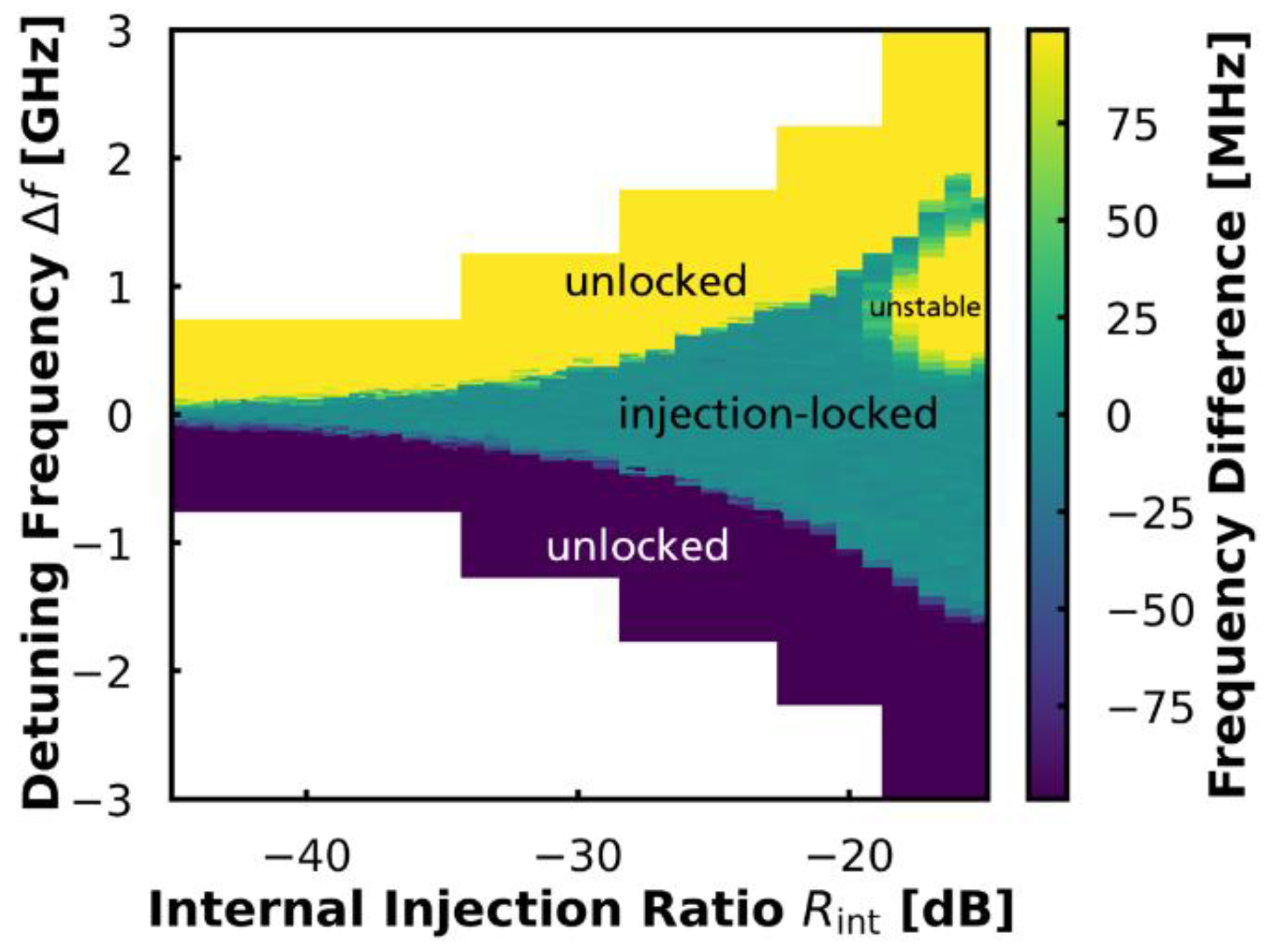
Figure 3.
(a) InP chip with two cascaded PMs for generating OFC, SOA is integrated after the second PM and the coupling interfaces are facilitated by spot-size-converters (SSCs); (b) Example of generated OFC spectrum. The measured OFC would support a bandwidth of 225 GHz.
Figure 3.
(a) InP chip with two cascaded PMs for generating OFC, SOA is integrated after the second PM and the coupling interfaces are facilitated by spot-size-converters (SSCs); (b) Example of generated OFC spectrum. The measured OFC would support a bandwidth of 225 GHz.
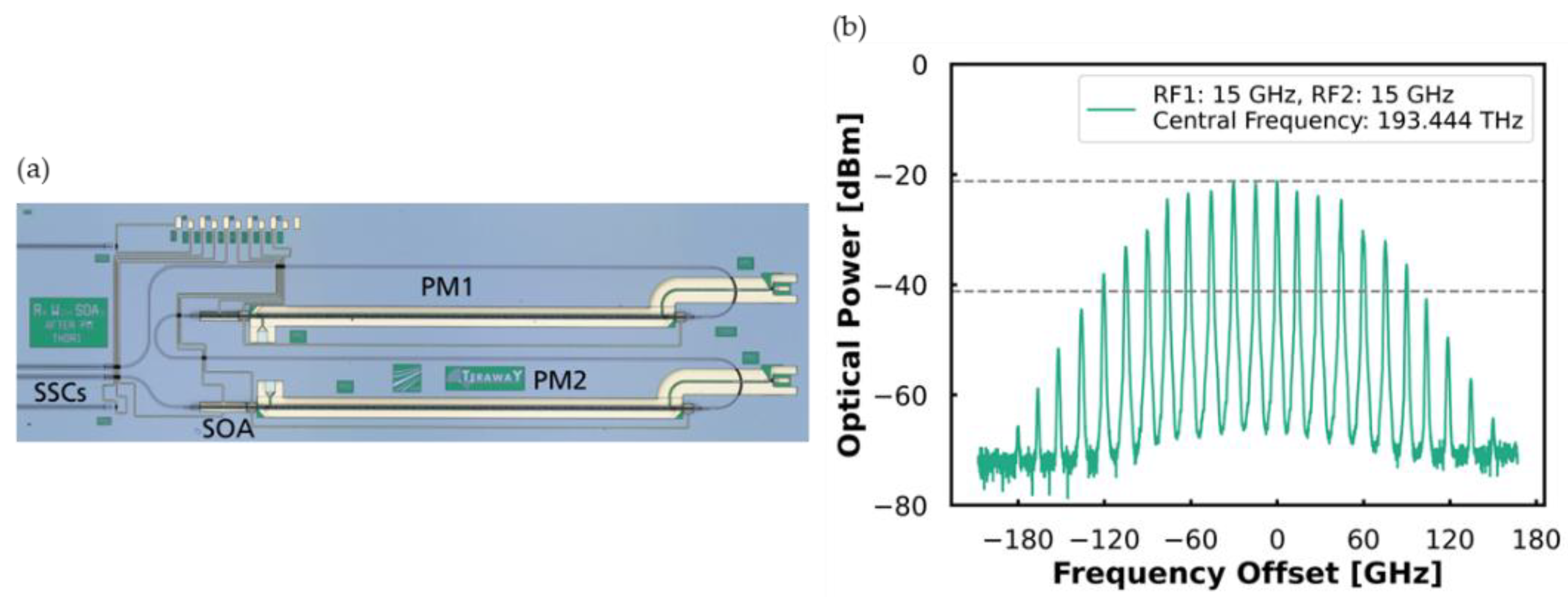
Figure 4.
Characterization of an InP Mach-Zehnder Modulator (MZM): (a) DC extinction ratio map of a 5 mm long MZM [15]; (b) High-frequency response of InP MZM with different length [15]; (c) Eye diagrams of a 5 mm long MZM for NRZ 64 Gbps, NRZ 80 Gbps, PAM4 24 GBd. [15].
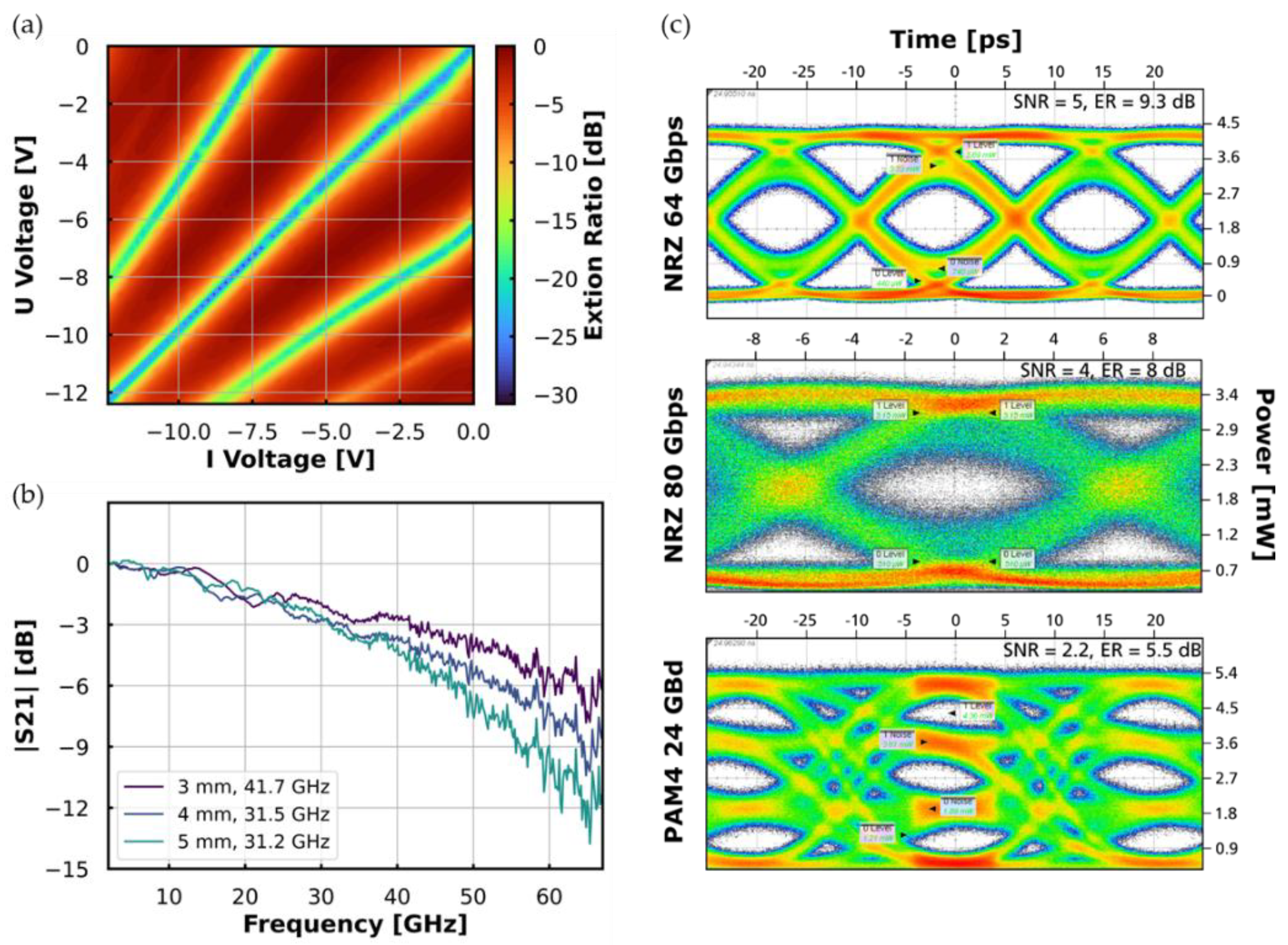
Figure 5.
(a) Close-up picture of the on-chip integrated optical isolator; (b) Characterization of such optical isolator [30].
Figure 5.
(a) Close-up picture of the on-chip integrated optical isolator; (b) Characterization of such optical isolator [30].
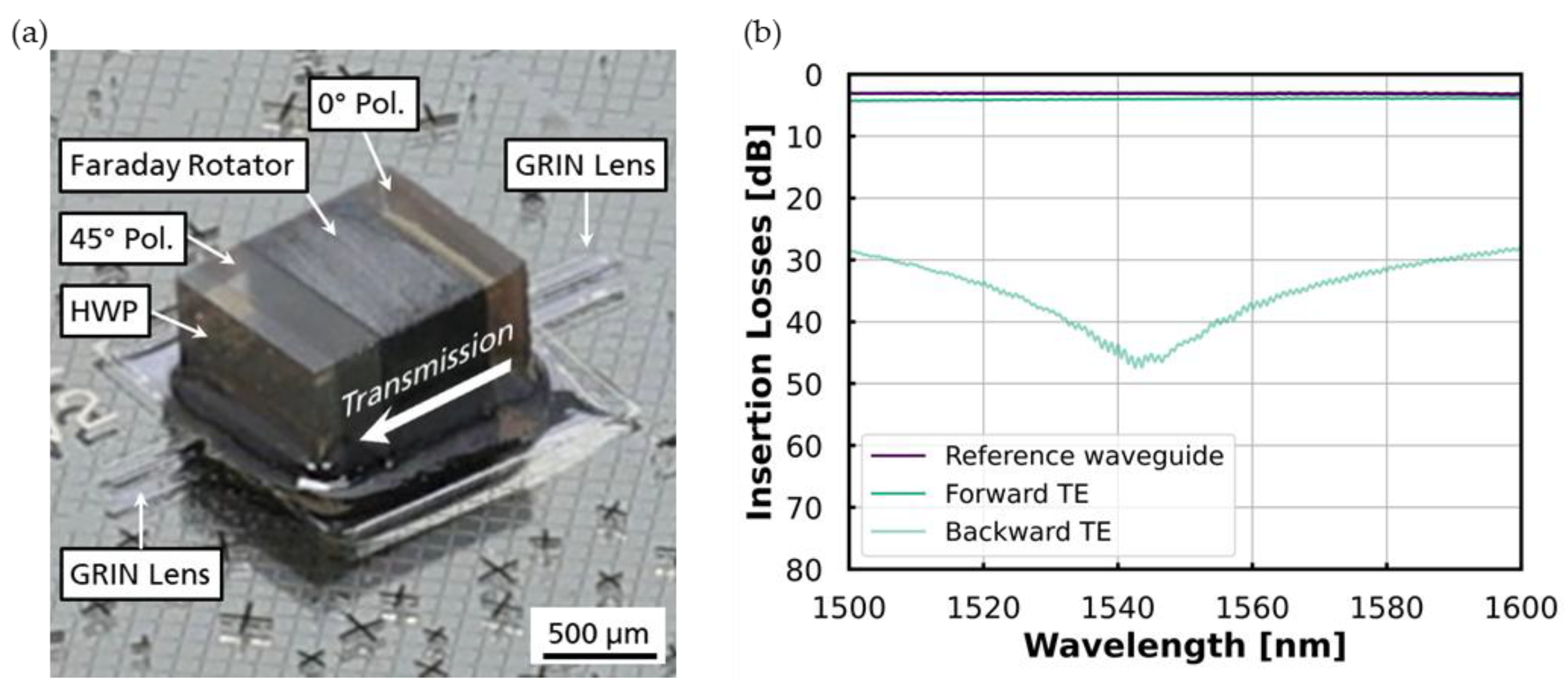
Figure 6.
(a) Photomixing scheme of an I/Q modulated optical beat signal using a PIN-PD. (b) Micrograph and scanning electron micrograph of a waveguide-integrated PD chip with bow-tie antenna for THz radiation.
Figure 6.
(a) Photomixing scheme of an I/Q modulated optical beat signal using a PIN-PD. (b) Micrograph and scanning electron micrograph of a waveguide-integrated PD chip with bow-tie antenna for THz radiation.
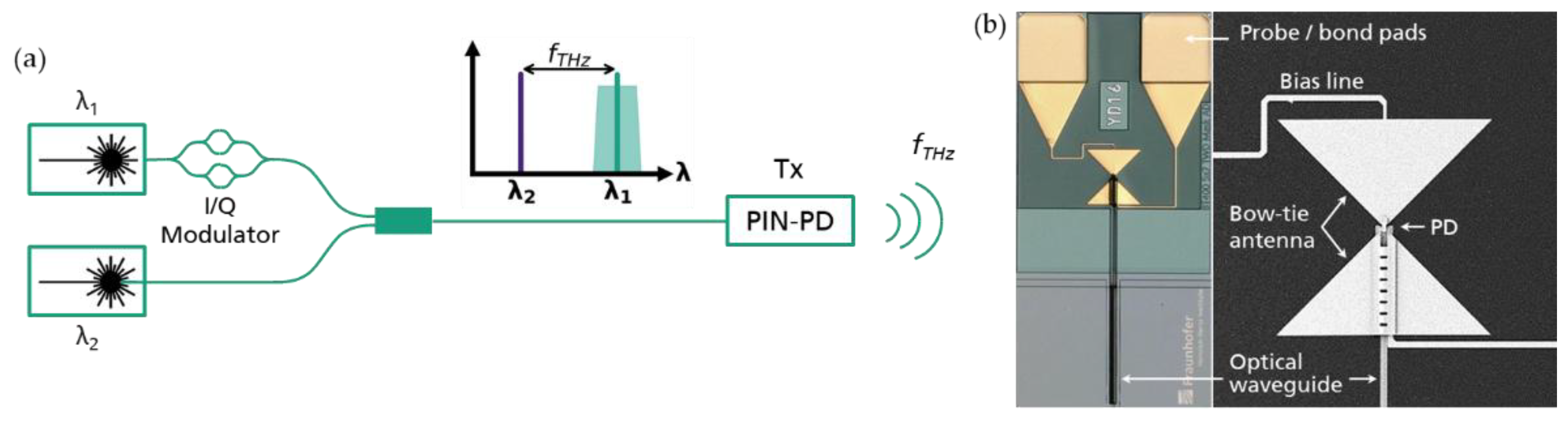
Figure 7.
(a) Photomixing of an optical beat signal using a PCA. (b) Micrograph and scanning electron micrograph of the novel waveguide-integrated PCAs [63].
Figure 7.
(a) Photomixing of an optical beat signal using a PCA. (b) Micrograph and scanning electron micrograph of the novel waveguide-integrated PCAs [63].
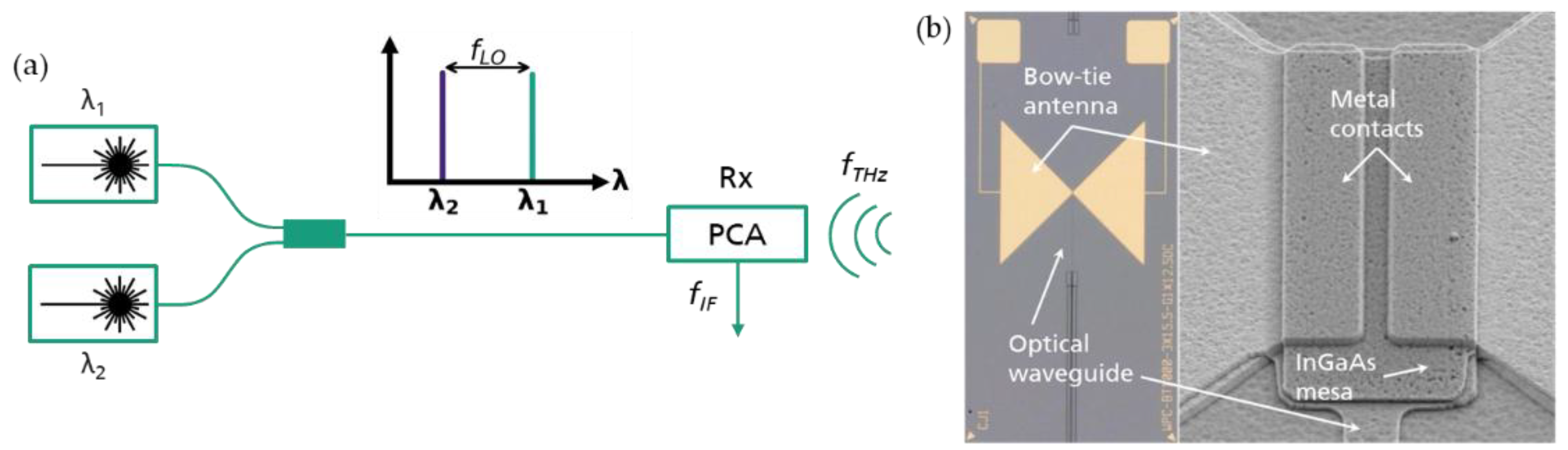
Figure 8.
(a) Micrograph of the fabricated 1x4 THz emitter array based on PIN-PD and integrated with SOA [65]. (b) The CAD model of packaging such antenna array [65]. (c) The packaged module [65].
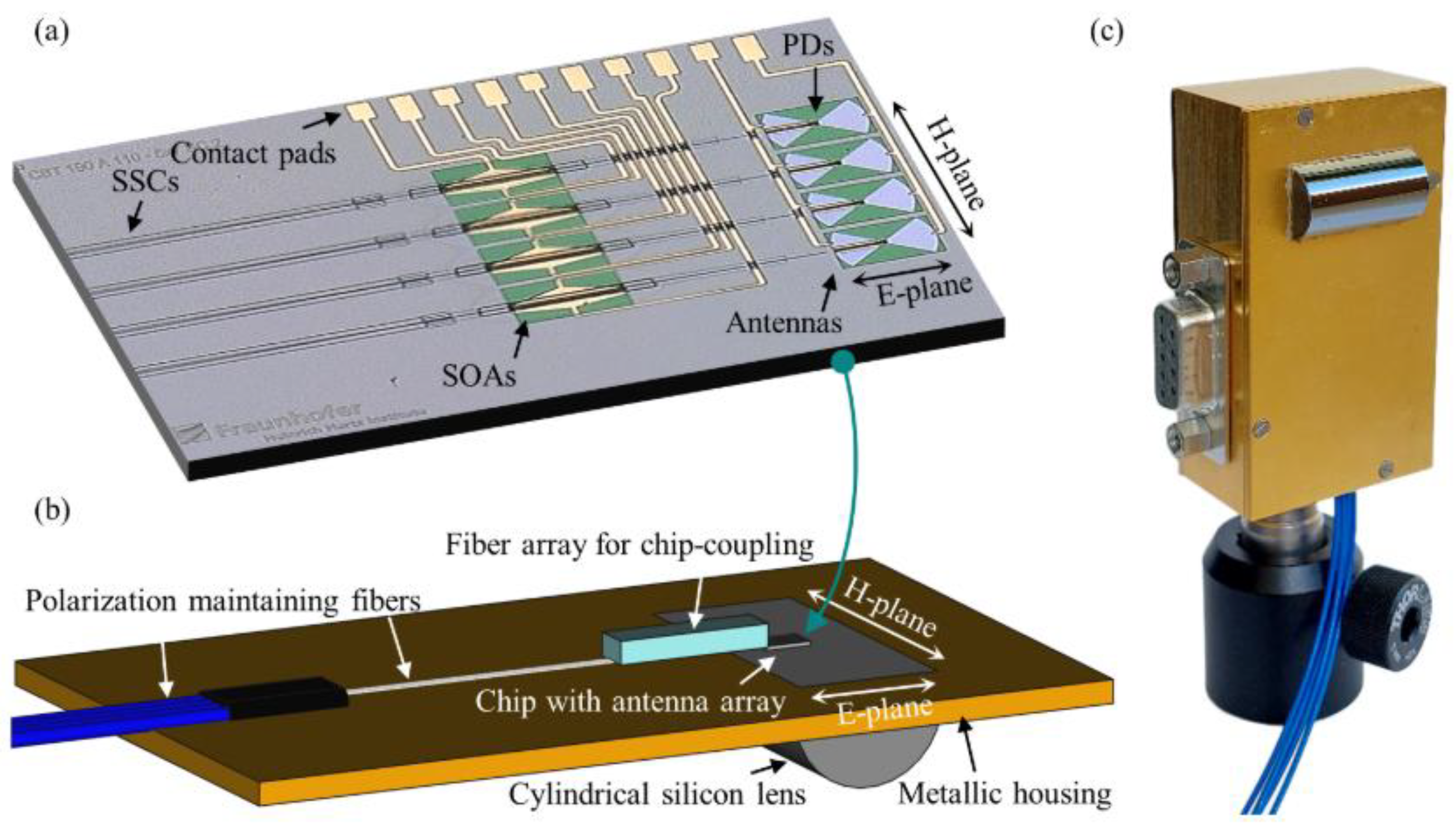
Figure 9.
Micrograph of fabricated 1x4 THz receiver array based on waveguide integrated PCA.
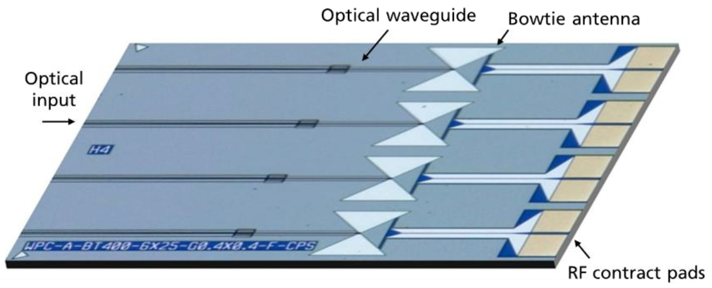
Figure 10.
Illustration of the schematic design of optical phased array (OPA) targeted for THz beam steering.
Figure 10.
Illustration of the schematic design of optical phased array (OPA) targeted for THz beam steering.
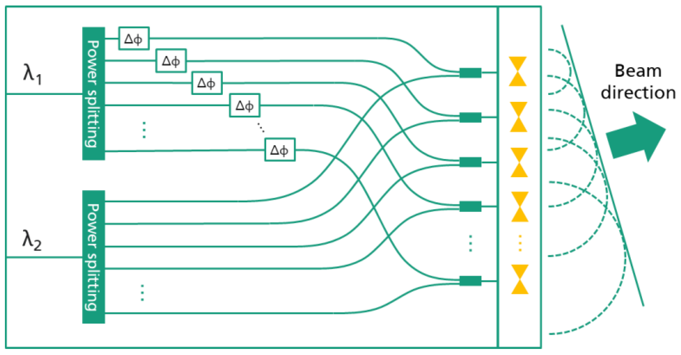
Figure 11.
(a) Photograph of the assembled and packaged OPA chip. Wire bonding to a multi-pin plug allows stable connection and driving of the OPA in the beam steering testbed. The augmented micrograph (b) shows the polymer-based OPA chip with 4 thermo-optical phase shifters to set the phase of the beat signal at the respective output port [65].
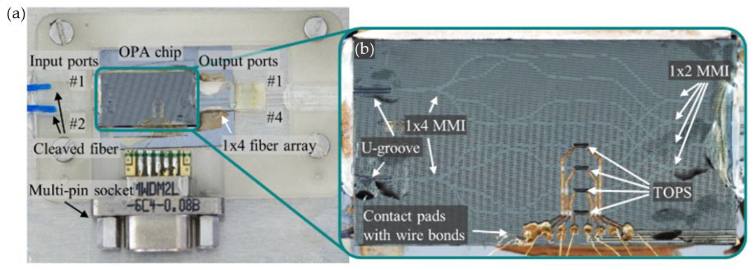
Figure 12.
Cross section of (a) InP spot-size converter; (b) PolyBoard taper; (c) Si3N4 waveguide with high-index-contrast (HIC) (left) and low-index-contract (LIC) (right) [17]. Simulation of power transmission between different waveguide interfaces: d) InP and PolyBoard; e) Si3N4 HIC and PolyBoard; f) Si3N4 LIC and PolyBoard.
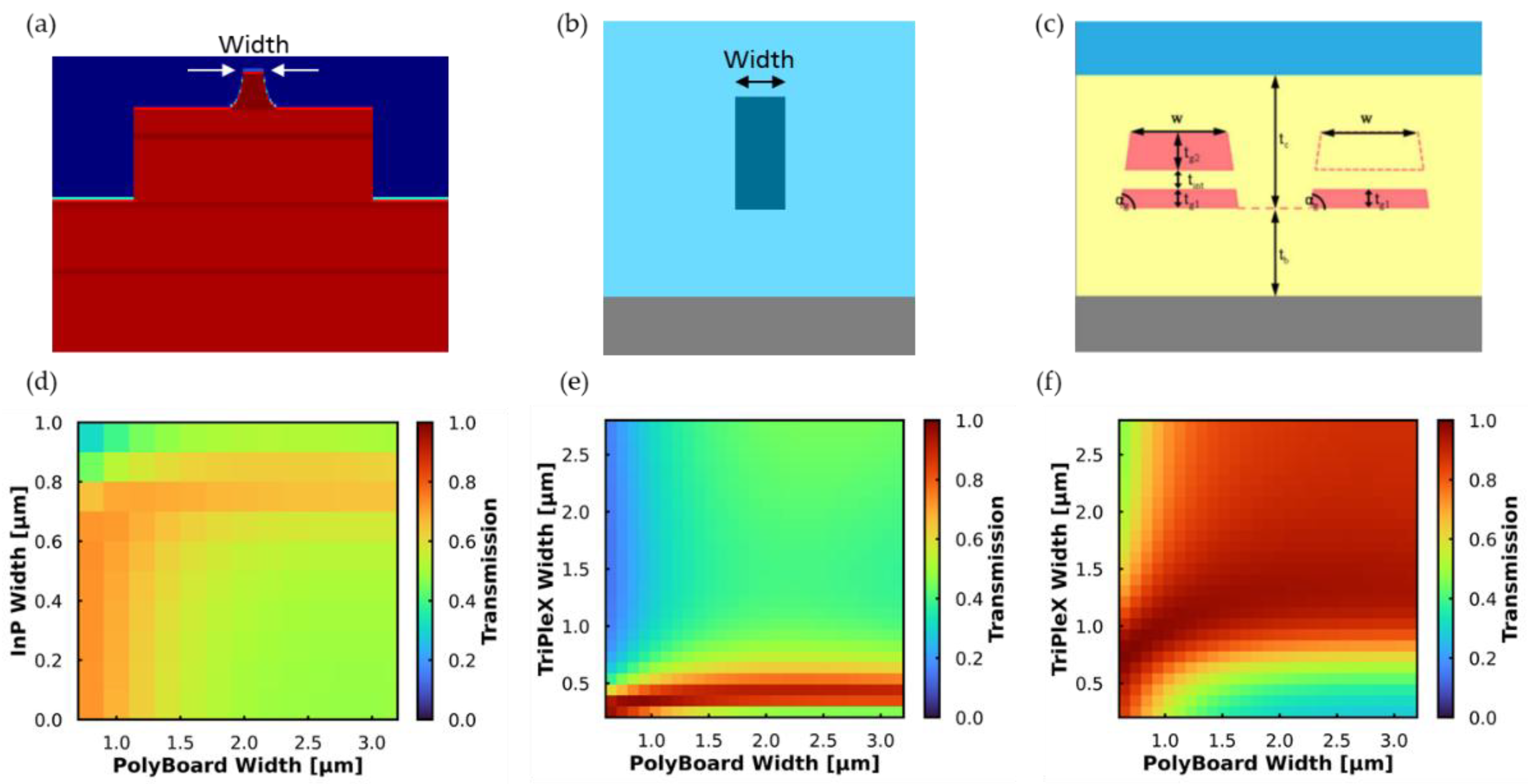
Figure 13.
Hybrid wireless transmitter PIC integrating InP, PolyBoard and Si3N4 platforms.
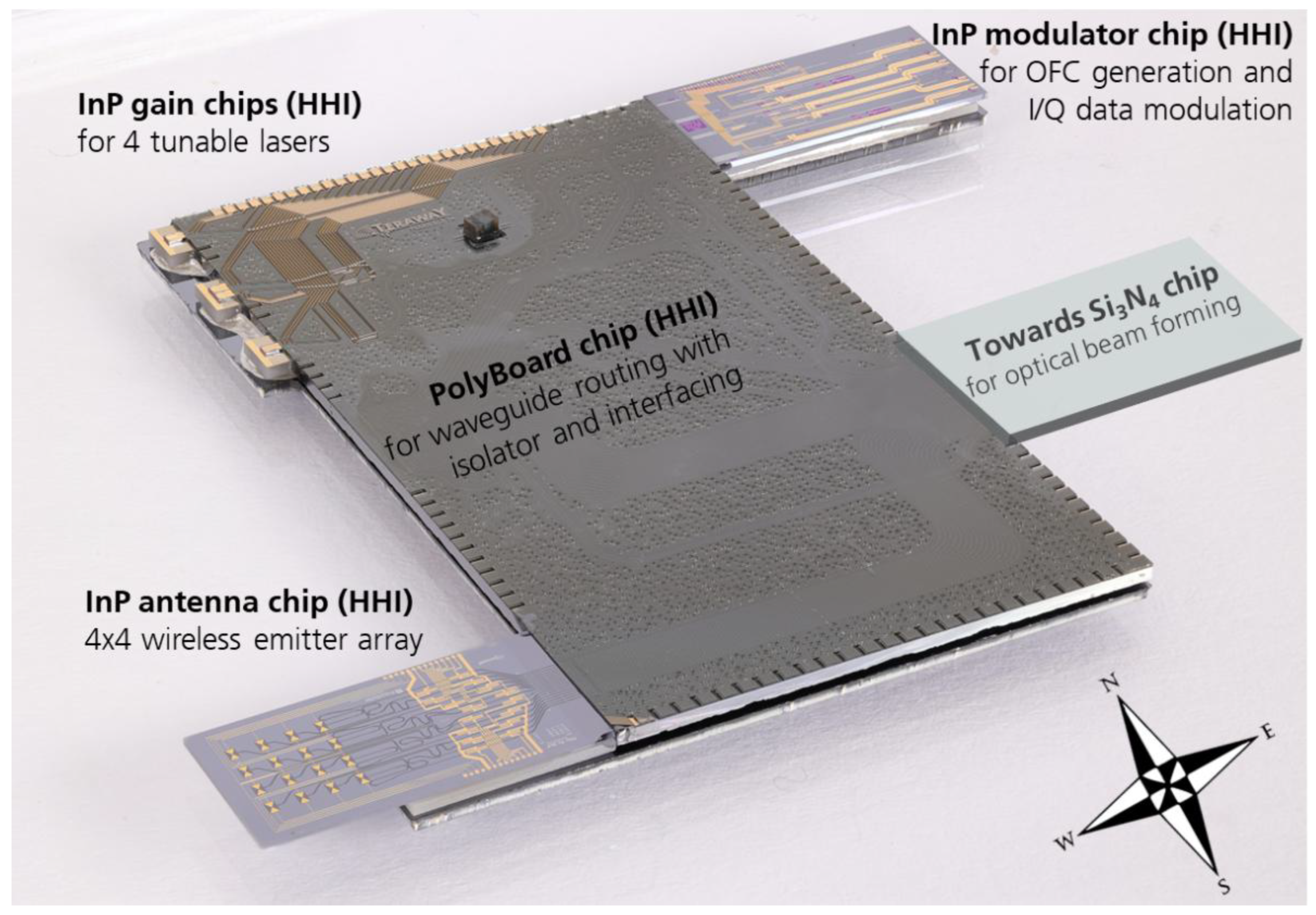
Figure 14.
Characterization of the assembled THz transmitter PIC. By varying the power applied onto the grating heater, tuning spectra has been recorded: (a) the master laser going through the InP modulator PIC; (b) The slave laser going through the InP modulator PIC; (c) The slave laser measured directly using a fiber array. (d) Comparison between fiber-chip and chip-chip characterization using the outmost SOAs of their generated photocurrent at different optical power level.
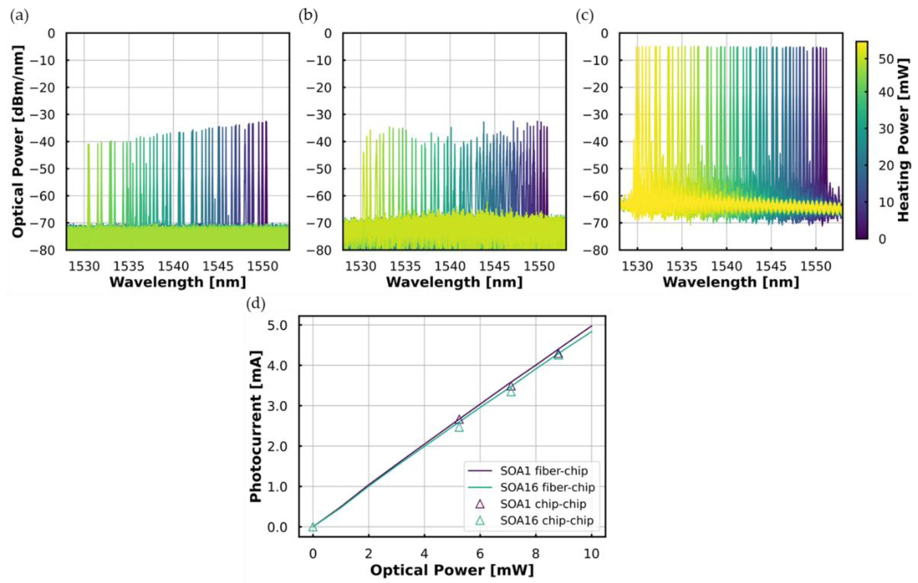
Figure 15.
Hybrid wireless receiver PIC integrating InP, PolyBoard platforms.
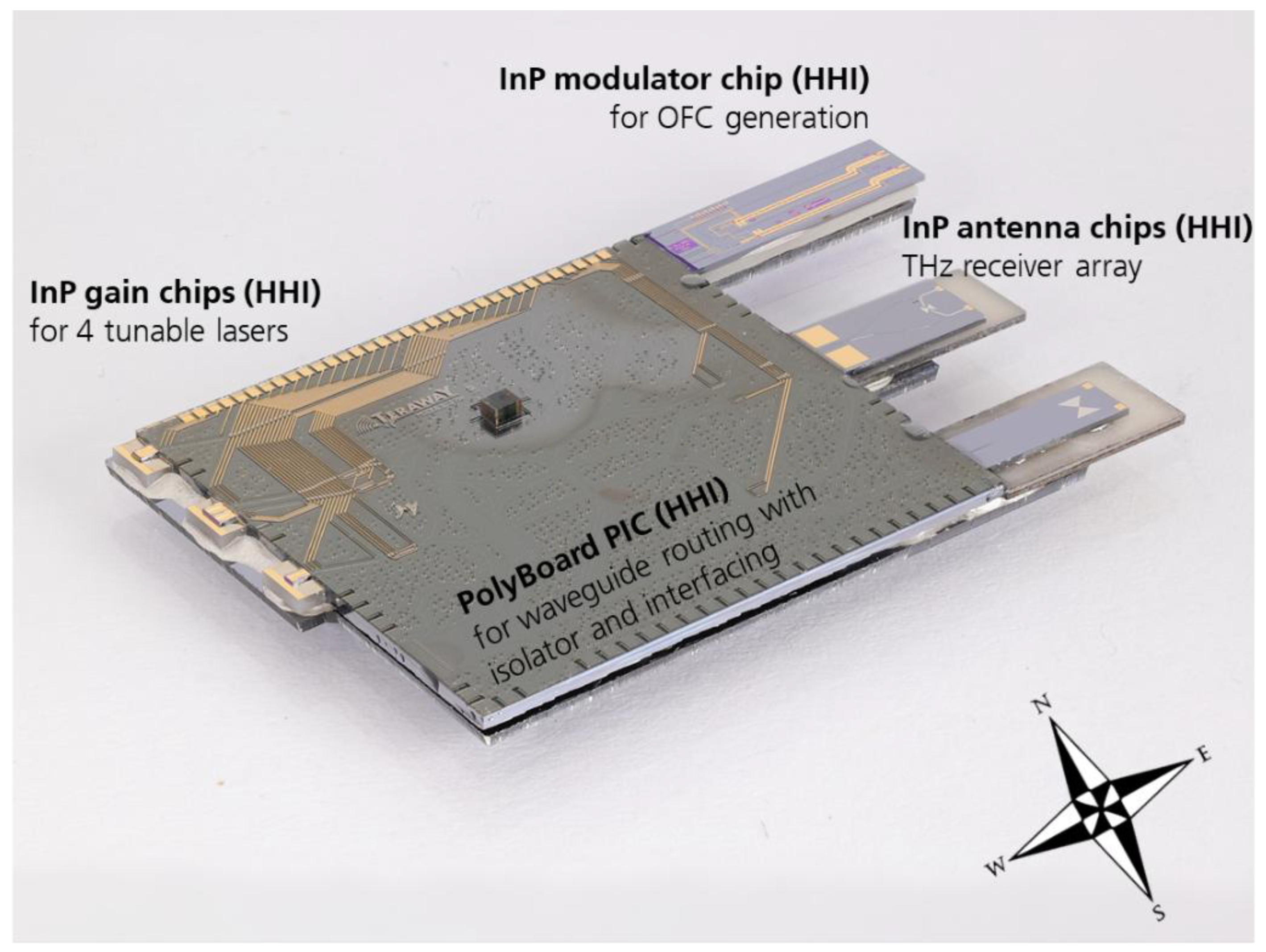
Figure 16.
Characterization of the assembled THz receiver PIC. By varying the power applied onto the grating heater, tuning spectra has been recorded: (a) The master laser going through the InP modulator chip; (b) The slave laser 1; (c) The slave laser 2. (d) Comparison between fiber-chip and chip-chip characterization of the 2-channel PCA at different optical power level. (e) On-chip OFC generated through the cascaded phase modulators and measured through the test ports [73]. (f) Phase-locked optical beat note measured at 45 GHz [73].
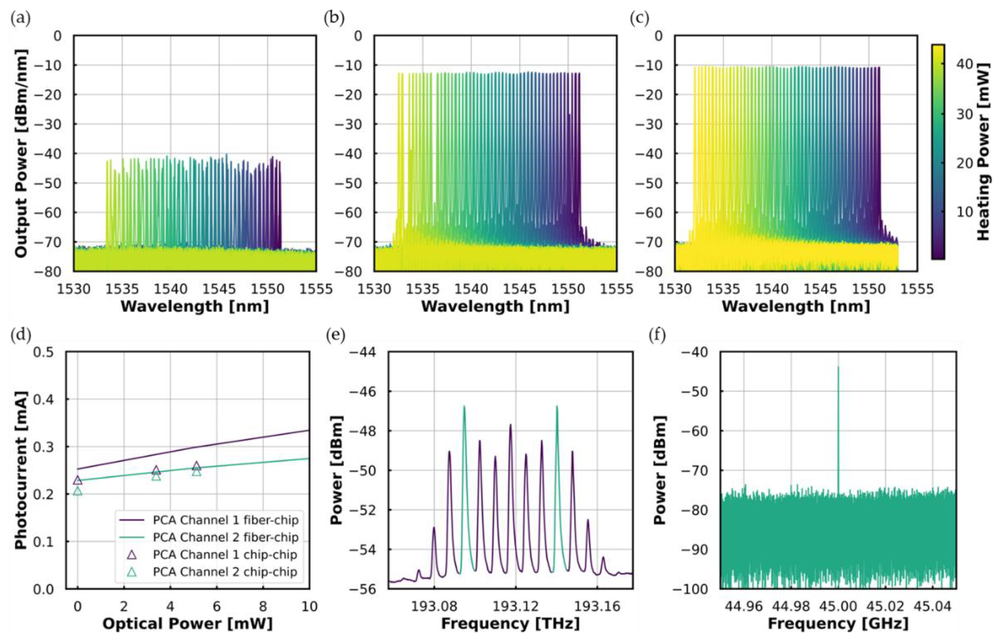

Table 1.
Qualitative comparison of functionalities offered on different photonic platforms. N/A = not available; + = possible; ++ = good; +++ = very good.
Table 1.
Qualitative comparison of functionalities offered on different photonic platforms. N/A = not available; + = possible; ++ = good; +++ = very good.
| Platforms | Waveguide Loss |
Routing capability | High Speed Modulation |
Tunable Lasers |
Optical isolator |
O/E functionalities (e.g. THz antenna) |
|---|---|---|---|---|---|---|
| InP | + | + | +++ | ++ | N/A | +++ |
| PolyBoard | ++ | +++ | N/A | +++ | + | N/A |
| Si3N4 | +++ | +++ | N/A | +++ | N/A | N/A |
Table 2.
Waveguide properties of each material platform.
| Platforms | neff @1550 nm | MFDx,y [µm] | Waveguide Width [µm] | Simulated coupling Loss towards PolyBoard [dB] |
|---|---|---|---|---|
| InP [16] | 3.2 | (3.5, 4.4) – (10.0, 7.0) | [0.1 – 1.0] | 1.5 |
| PolyBoard | 1.46 – 1.45 | (4.3, 4.3) – (9.0, 7.8) | [0.8 – 3.2] | N/A |
| Si3N4 [17] | 1.535 – 1.446 | (1.5, 1.2) – (10.0, 10.0) | [0.8 – 3.7] | 0.1 |
Disclaimer/Publisher’s Note: The statements, opinions and data contained in all publications are solely those of the individual author(s) and contributor(s) and not of MDPI and/or the editor(s). MDPI and/or the editor(s) disclaim responsibility for any injury to people or property resulting from any ideas, methods, instructions or products referred to in the content. |
© 2025 by the authors. Licensee MDPI, Basel, Switzerland. This article is an open access article distributed under the terms and conditions of the Creative Commons Attribution (CC BY) license (http://creativecommons.org/licenses/by/4.0/).
Copyright: This open access article is published under a Creative Commons CC BY 4.0 license, which permit the free download, distribution, and reuse, provided that the author and preprint are cited in any reuse.


