Submitted:
07 March 2025
Posted:
10 March 2025
You are already at the latest version
Abstract
Additive manufacturing (AM) technologies allow for the creation of components with greater design flexibility. The complexity in geometry and composition can enhance functionality, while parts made from multiple materials have the capacity to deliver improved performance. Nonetheless, most multimaterial printing methods are still in their infancy and face numerous challenges. Numerous materials require individual post-treatment, and some may not be compatible with each other regarding shrinkage, melting or sintering temperatures, and interactions.
In this study, we introduce a technique for producing a metal-ceramic multimaterial prototype for electronic packages through powder-bed additive manufacturing technology, specifically selective laser melting (SLM). A composite based on silicon carbide was created. The powder was removed from the chamber to prevent cross-contamination, and molybdenum-based powder was introduced. Molybdenum tracks with a diameter of 400μm and a length of 15mm were produced using SLM on a SiC layer.
The results indicated that the SiC-based samples exhibit a relatively uniform microstructure with homogeneously distributed porosity. Mo-based powder containing 5% silicon was successfully SLM-ed on SiC layer. The surface of Mo layer surface is smooth with some cracks. The microstructure and chemical analysis of the layer was performed. The Vickers hardness was measured.
Keywords:
selective laser melting
; multilayer manufacturing
; silicon carbide
; molybdenum silicide
; molybdenum
1. Introduction
Molybdenum is a refractory metal which possesses a high melting point (2623 °C)[1], high thermal conductivity (139 W/mK) [1], low electrical resistivity (5.46*108mΩ) [2], small thermal expansion coefficient (4.8 x 10⁻⁶/K) [3] and large elastic modulus at room temperature. Such combination of properties, make molybdenum a useful material for electronic packages. The thermal conductivity and low specific heat enable Mo to be heated and cooled quickly, making it particularly beneficial in electrical applications. The thermal expansion coefficient is similar to that of silicon and borosilicate glass at cryogenic temperatures, which renders molybdenum a suitable option for space electronics applications [4]. Molybdenum possesses one of the highest melting points among other elements, yet it is prone to oxidation at elevated temperatures. The poor oxidation resistance of pure Mo can be improved when adding such elements as silicon or boron [5].
Oxidation of Mo is repeatedly mentioned as a limiting factor in some applications, or at least a consideration, because mass loss due to oxidation in Mo and its alloys reduces strength compared to an intact specimen. Another limitation in application is the cost of molybdenum.
Additive Manufacturing can produce intricate structural designs with improved functionality and reduced waste. This may lower the expenses of the components and broaden the application. Despite the high melting temperature, molybdenum is possible to manufacture by selective laser melting (SLM) technology. There are attempts to manufacture Mo by SLM [6,7,8,9,10,11]. Faidel et al. studied the influence of layer thickness, scanning velocity and overlap on the density and microstructure of the Mo [12]. They achieved 82.5% density applying laser power of 200W. To enhance density, it was advised to utilize increased laser power and reduce layer thickness. Kaserer et al. [13] solved the problem with crack formation adding 0.45wt% carbon to molybdenum. They reveal that carbon changes solidification mode, resulting in a larger grain boundary area while minimizing segregated oxygen. Carbon reacts with leftover oxygen in the build chamber and CO eliminates, which is the reason for the lower C and oxygen levels in the final material. The influence of carbon addition to molybdenum also improves the mechanical properties (Table 1). The substrate temperature was necessary to eliminate the cracks and achieve full density. Wang et al. [14] consider that the crack formation during the SLM can be prevented by applying layer-wise scanning rotation. Moreover, high laser power and a tiny structure of supports was proposed to slow the heat transfer and achieve crack-less microstructure of dense molybdenum without adding carbon. The supports allowed the printed components to withstand elevated temperatures for an extended period during heating by providing a low rate of heat elimination.
Higashi [15] investigated the influence of process parameters on the defect formation, focusing on porosity, crystallographic texture, and the characteristics of the melt pool during SLM of Mo. Over 99% theoretical density was achieved applying >150 J/mm3 volumetric energy density (VED). The influence of VED on the porosity was especially significant at higher layer thickness. It was found that scan speed had a direct impact on the properties of the crystallographic texture.
Kinkade evaluated the influence of energy density, scanning techniques, and environments on the mechanical properties of Mo and Mo alloyed with Rhenium [16]. Similar to other research, Kinkade acknowledged that increased VED resulted in greater densities and improved mechanical characteristics. Eckley et al. [17] revealed that the flexural strength of the printed Mo and Mo-Re alloys enhances when SLM is performed in an argon-3% hydrogen gas environment. However, they exhibited a large degree of anisotropy in mechanical properties that is affected by the build direction. The mechanical properties significantly decreased with increasing scanning speed when printed in the argon-3% hydrogen environment. While there is minimal sensitivity of scanning speed to flexural strength when manufacturing in an argon environment. Conversely, Bustin concluded that the change in H2 amount within the build atmosphere generated only minor effects on the outcomes when compared to laser speed and test temperature [18]. The author suggests using a sufficiently high VED to completely melt the material and minimize porosity, while also maintaining a low laser speed.
The reason for formation of pores and cracks can be different [19]. At lower energy density the temperature of the molten pool is low, and the liquid phase volume is not enough to fill the voids. At higher energy density Marangoni flow can drag gas forming pores. The formation of the cracks is mainly explained by the fast solidification of the molten pool. Molybdenum has high thermal conductivity [20] which leads to a high cooling rate. The solidified part shrinks, creating stresses and strain, which forms cracks. It is proposed that the high oxidation sensitivity and low wettability of molybdenum also contributes to crack formation. The oxygen which accumulates in grain boundaries in form of oxide has high evaporation pressure resulting in increased spatter formation and an alteration of the Marangoni convection [21]. Crack formation can be inhibited by adding reinforcements [22], adding a support structure, suppressing the oxygen content [19] or decrease the thermal stresses by heating the powder bed [21].
The aim of this work is to manufacture molybdenum-based alloy on silicon carbide substrate using selective laser melting technology. The idea is developed technology to manufacture multimaterial component in one stage SLM. Silicon carbide containing 10 wt.% BN substrate was prepared by SLM technology [23]. The powder was eliminated from the powder bed, and molybdenium-silicon powder was loaded for laser melting.
2. Materials and Methods
Silicon carbide-based substrate manufacturing technology is described by Ghaltaghchyan et al. [23]. Then the powder was eliminated from the chamber. The chamber was polished and Mo-5Si powder was placed.
The Mo-5Si powder feedstock was prepared using 95 wt.% molybdenum (Truer, particle size 15-40 μm, purity ≥99.9% trace metals basis) and 5 wt.% silicon (Silgrain, particle size 10-30 μm). The powders were placed in a zirconia jar along with 10 mm zirconia balls. The powder-to-ball mass ratio was 1:2 by weight. The jar was rotated for 2 hours at 50 rpm.
The selective laser melting process was performed using the Realizer GmbH SLM-50 system in Germany, with a 120 W continuous fibre laser (YAG: Nd³⁺) with a wavelength of 1.06 μm. Molybdenum -5wt.% silicon (Mo-5Si) tracks with diameter of 100 μm and 400μm and length of 15mm were SLM-ed on SiC layer. To understand the possible reactions under SLM, solid samples of Mo-5Si were built with dimensions of 5 x 8.5 x 0.5 mm. Laser parameters included a power: 80 W, layer thickness: 30 μm, hatch distance: 0.06mm, exposure time: 40µs, point distance: 20µm. Continuous scanning was carried out with a 90-degree rotation between layers. Additionally, the silicon carbide baseplate was preheated up to 100°C․
To assess porosity and microstructural features, rectangular samples were surface polished using a universal grinding and polishing device, the Qpol Go (Mammelzen, Germany). Microstructural characterization was performed by scanning electron microscope (SEM, Zeiss, Evo 10) equipped with an EDS detector. Samples were coated with a 30 nm layer of gold to ensure sufficient conductivity. Phase characterization was done by Mini Flex 600 X-ray diffractometer, Rigaku (40 mA, 40 kV, Cu Kα radiation, λ = 0.1542 nm, step size of 0.02°).
The Vickers hardness of the samples was measured using the FALCON 600G2FA. A load of 1.0 kgf was applied for a dwell time of 10 seconds. Measurements were conducted at room temperature, with multiple microhardness tests performed at different positions to determine the mean value.
3. Results and Discussion
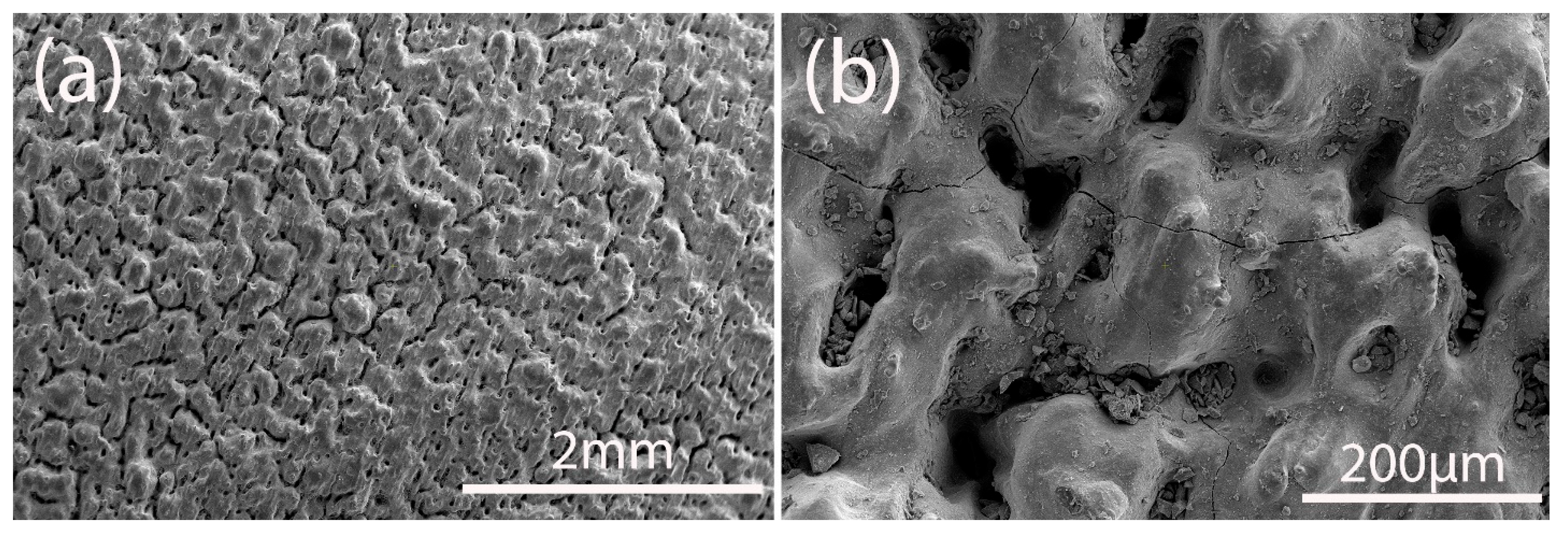
Silicon carbide-based substrate was successfully manufactured. The grains are connected to each other with necks with clear orientation. This orientation corresponds to scanning orientation. The grains are few times bigger than the initial powder particles size. The sintering happened through liquid phase formation under the laser, which regrouped the particles. The pores are distributed between the grains (Figure 4 (a)). There are cracks on the SiC-based substrate, which can be caused by the fast heating and cooling rate of the laser sintering combined with high thermal conductivity of silicon carbide (Figure 4(b)).
Figure 1.
Microstructure of SiC-based substrate under (a) low, and (b) high magnification.
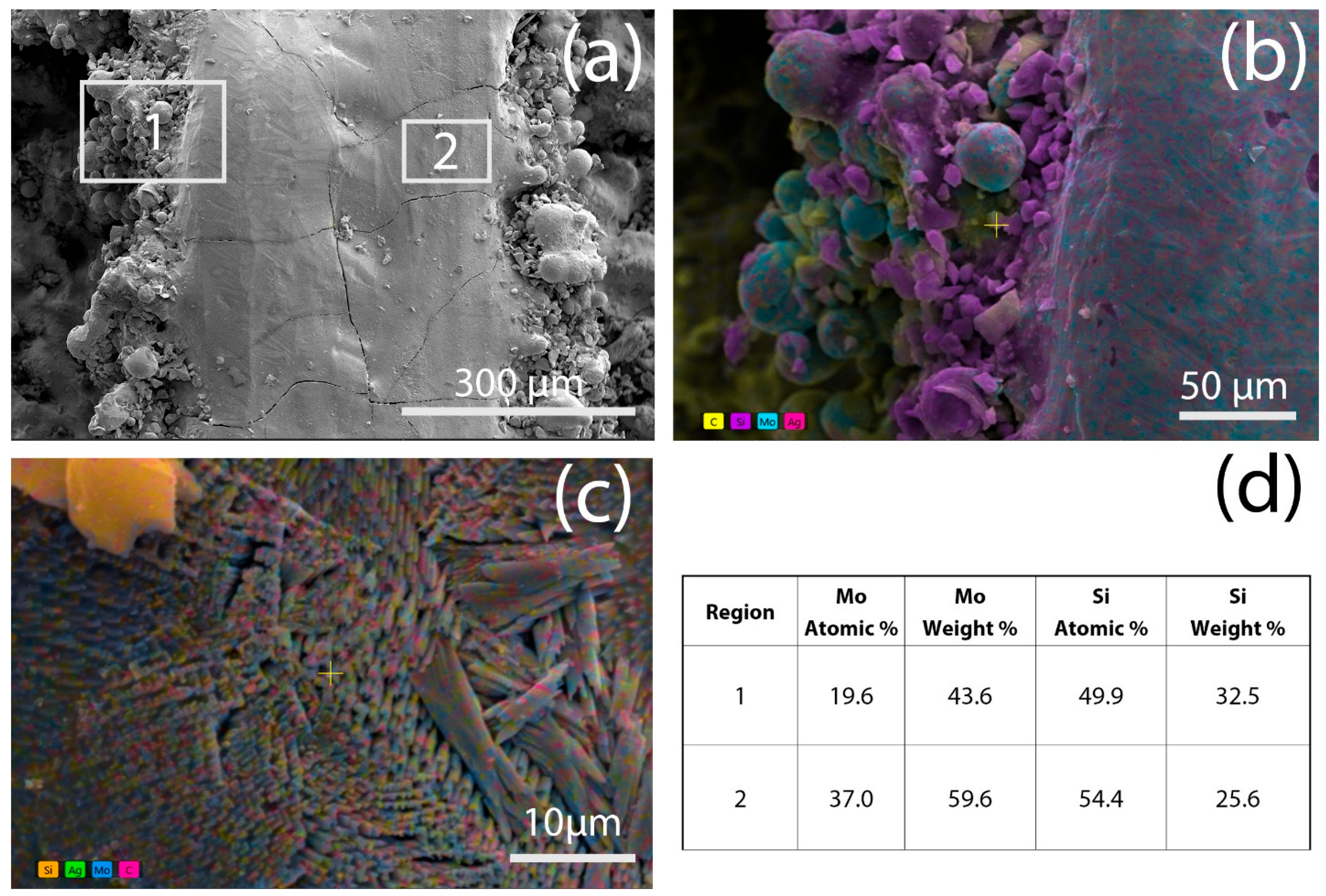
The surface of the Mo layer is smoother (Figure 2(a)). There are cracks on the metal track, which is typical for SLM of molybdenum. the formation of cracks is due to high thermal conductivity, resulting in rapid solidification following the laser's passage over the melting pool. We have used silicon which was believed to react with molybdenum generating energy [24]. The generated energy was proposed to decrease the thermal diffusion rate. Moreover, the formed molybdenum silicides were proposed to prevent crack propagation. According to the EDS study, MoSi2 based spherical grains form on the edge of the Molybdenum track (Figure 2(b)). In the middle of the track there are submicron sized fibers with Mo:Si atomic ratio of 37:54.4 are formed (Figure 2(c-d)).
Figure 2.
Microstructure of (a) Mo-5Si track, (b) high magnification image of Region 1, (c) high magnification image of Region 2, (d) EDS analyses of Region 1 and 2.
Figure 2.
Microstructure of (a) Mo-5Si track, (b) high magnification image of Region 1, (c) high magnification image of Region 2, (d) EDS analyses of Region 1 and 2.
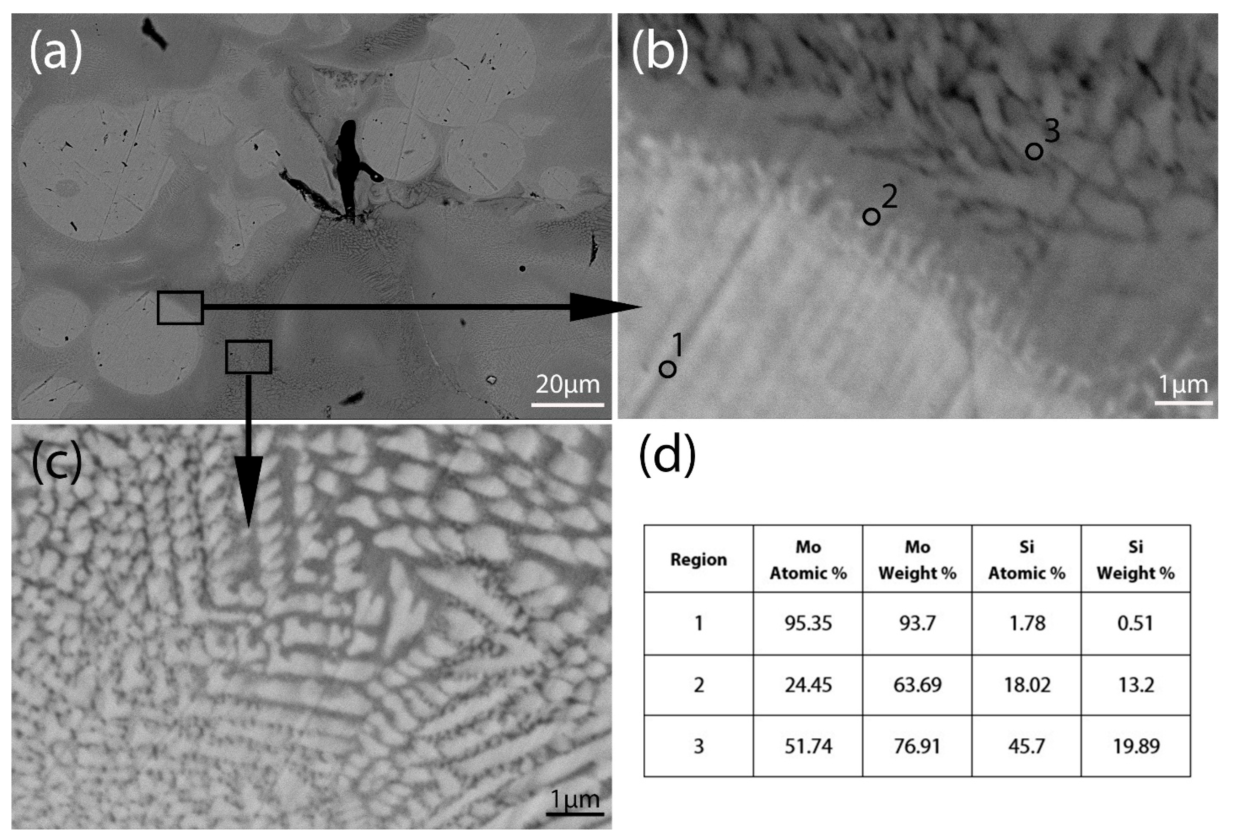
To understand the possible phases formed during Mo-Si laser melting, samples with 0.5 x 10.0 x 0.4mm size were SLM-ed. The microstructure of the cross section of the sample is illustrated in Figure 3 (a). The EDS analysis shows that the grains are composed of mainly molybdenum (region 1), which is covered with a silicide layer (region 2) (Figure 3(b)). The EDS analysis shows that the layer contains high amount of molybdenum, which corresponds to Mo5Si3 phase. Between Molybdenum particles there is a lumpy structure (Figure 3 (c)). The lumpy mass contains more molybdenum according to EDS results (Figure 3(d)).
Figure 3.
Microstructure of the polished cross section of Mo-5Si bulk sample (a) low magnification, (b) high magnification image of the grain border, (c) high magnification image of the intergranular space.
Figure 3.
Microstructure of the polished cross section of Mo-5Si bulk sample (a) low magnification, (b) high magnification image of the grain border, (c) high magnification image of the intergranular space.
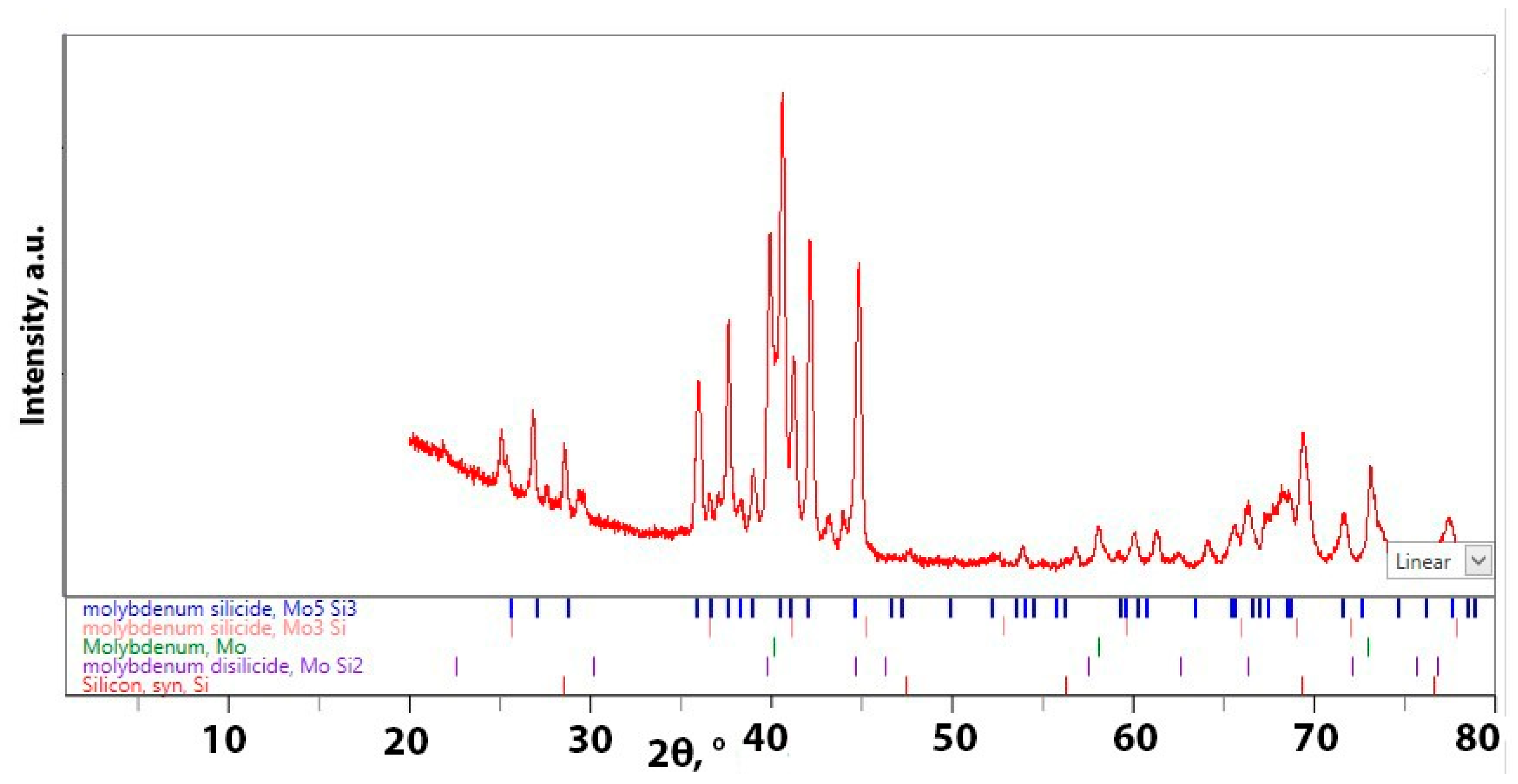
The XRD analysis shows that the Mo5Si3 phase was primarily the main silicide formed during SLM (Figure 4). However, some MoSi2 and traces of Mo3Si were also formed. It is revealed that Mo5Si3 is generated due to solid-solid interaction during the preheating period [25]. MoSi2 phase forms just after silicon melts [26]. The Mo and MoSi2 dissolves in Si melt. When silicon melt becomes saturated or supersaturated Mo5Si3 and Mo3Si precipitate. It is revealed that Mo5Si3 and Mo3Si are formed in the absence of silicon melt. Mo5Si3 has higher formation enthalpy than Mo3Si, hence formation of Mo5Si3 phase is more likely [27]. The presence of Mo3Si could be caused by the diffusion interaction of Mo with Mo5Si3, which takes longer time.
Figure 4.
XRD of Mo-5Si sample.
Mechanical Properties
Vickers hardness of the samples were measured applying 1.0 kgf load. There are radial microcracks generated from one or two sides of the indentation. As the microcracks are not linear and have different length the fracture toughness is not measure. The value of Vickers hardness of the selective laser melted Mo-5Si is 740 ± 0.3 GPa.
4. Conclusion
Selective laser melting was successfully applied to obtain multilayer metal-ceramic based composites in one stage. Silicon carbide layer manufactured by SLM has porosity. Molybdenum mixed with 5 wt.% silicon was SLM-ed on SiC layer with smooth surface. Molybdenum reacted with silicon during laser melting process. Molybdenum silicides were formed. The Vickers hardness of the obtained Mo-based layer was measured to be 740 ± 0.3 GPa.
References
- J. Sarkar, Sputtering Targets and Thin Films for Flat Panel Displays and Photovoltaics, in: Sputtering Materials for VLSI and Thin Film Devices, Elsevier, 2014: pp. 417–499. [CrossRef]
- D. Rafaja, H. Köstenbauer, U. Mühle, C. Löffler, G. Schreiber, M. Kathrein, J. Winkler, Effect of the deposition process and substrate temperature on the microstructure defects and electrical conductivity of molybdenum thin films. Thin Solid Films 2013, 528, 42–48. [CrossRef]
- P. Hidnert, W.B. Gero, Thermal expansion of molybdenum, Scientific Papers of the Bureau of Standards. 1924, 19, 429. [CrossRef]
- W. Su, M. Pan, D. Mo, H. Xu, Mechanical and thermal properties of Mo for packaging HgCdTe IRFPA detector at cryogenic temperatures. Infrared Phys Technol 2022, 127, 104373. [CrossRef]
- Douglas, M. Berczik, Method for enhancing the oxidation resistance of a molybdenum alloy, and a method of making a molybdenum alloy, 5,595.616, 1997.
- S. Guo, W. Zhou, Z. Zhou, N. Nomura, Laser additive manufacturing of pure molybdenum using freeze-dry pulsated orifice ejection method-produced powders. Journal of Materials Research and Technology 2022, 16, 1508–1516. [CrossRef]
- P. Rebesan, Characterization of Molybdenum produced by Laser Powder Bed Fusion for the high-temperature Ion sources of the INFN SPES facility, (2022).
- W. Ma, J. Ning, L.-J. Zhang, S.-J. Na, Regulation of microstructures and properties of molybdenum-silicon-boron alloy subjected to selective laser melting. J Manuf Process 2021, 69, 593–601. [CrossRef]
- Y. Wu, Q. Wu, M. Li, J. Wang, D. Yao, H. Luo, X. An, H. Fu, H. Zhang, X. Yang, Q. Zou, S. Li, H. Ji, X. Zhang, Numerical investigation on effects of operating conditions and final dimension predictions in laser powder bed fusion of molybdenum. Addit Manuf 2023, 76, 103783. [CrossRef]
- A. Leclercq, T. Mouret, V. Brailovski, Laser powder bed fusion of molybdenum: Density, structure and mechanical properties at room and elevated temperatures. Materials Science and Engineering: A 2025, 929, 148004. [CrossRef]
- N. Alinejadian, P. Wang, L. Kollo, K.G. Prashanth, Selective Laser Melting of Commercially Pure Molybdenum by Laser Rescanning, 3D Print Addit Manuf 2023, 10, 785–791. [CrossRef]
- D. Faidel, D. Jonas, G. Natour, W. Behr, Investigation of the selective laser melting process with molybdenum powder. Addit Manuf 2015, 8, 88–94. [CrossRef]
- L. Kaserer, J. Braun, J. Stajkovic, K.-H. Leitz, B. Tabernig, P. Singer, I. Letofsky-Papst, H. Kestler, G. Leichtfried, Fully dense and crack free molybdenum manufactured by Selective Laser Melting through alloying with carbon. Int J Refract Metals Hard Mater 2019, 84, 105000. [CrossRef]
- D. Wang, C. Yu, J. Ma, W. Liu, Z. Shen, Densification and crack suppression in selective laser melting of pure molybdenum. Mater Des 2017, 129, 44–52. [CrossRef]
- M. Higashi, T. Ozaki, Selective laser melting of pure molybdenum: Evolution of defect and crystallographic texture with process parameters. Mater Des 2020, 191, 108588. [CrossRef]
- R.X. Kinkade, C.C. R.X. Kinkade, C.C. Eckley, B.M. Sexton, T.E. Shelton, C.M. Schubert-Kabban, C.R. Hartsfield, J.S. Brewer, R.A. Kemnitz, Evaluating Molybdenum-Rhenium Alloys Through Additive Manufacturing, SSRN Electronic Journal (2022). [CrossRef]
- C. C. Eckley, R.X. Kinkade, B.M. Sexton, T.E. Shelton, C. Schubert-Kabban, C.R. Hartsfield, J.S. Brewer, R.A. Kemnitz, Evaluating Molybdenum-Rhenium Alloys Through Additive Manufacturing. JOM 2023, 75, 1928–1940. [CrossRef]
- Megan, L. Bustin, Additive Manufacturing of Molybdenum for High Temperature Structural Applications, 2022.
- A. Yan, A.M. Atif, X. Wang, T. Lan, Z. Wang, The Microstructure and Cracking Behaviors of Pure Molybdenum Fabricated by Selective Laser Melting. Materials 2022, 15, 6230. [CrossRef]
- André Lindemann, Measurement of the Thermophysical Properties of Pure Molybdenum, 2013.
- J. Braun, L. Kaserer, J. Stajkovic, K.-H. Leitz, B. Tabernig, P. Singer, P. Leibenguth, C. Gspan, H. Kestler, G. Leichtfried, Molybdenum and tungsten manufactured by selective laser melting: Analysis of defect structure and solidification mechanisms. Int J Refract Metals Hard Mater 2019, 84, 104999. [CrossRef]
- K. Li, D. Wang, L. Xing, Y. Wang, C. Yu, J. Chen, T. Zhang, J. Ma, W. Liu, Z. Shen, Crack suppression in additively manufactured tungsten by introducing secondary-phase nanoparticles into the matrix, Int J Refract Metals Hard Mater 2019, 79, 158–163. [CrossRef]
- T. Ghaltaghchyan, H. Khachatryan, K. Asatryan, V. Rstakyan, M. Aghayan, Effect of additives on selective laser sintering of silicon carbide. Boletín de La Sociedad Española de Cerámica y Vidrio 2023, 62, 504–514. [CrossRef]
- S. L. Kharatyan, M.A. Aghayan, H.A. Chatilyan, Interaction modes in Mo/Si diffusion couple at non-isothermal conditions. International Journal of Self-Propagating High-Temperature Synthesis 2014, 23, 138–140. [CrossRef]
- F. Baras, D.K. Kondepudi, F. Bernard, Combustion synthesis of MoSi2 and MoSi2–Mo5Si3 composites: Multilayer modeling and control of the microstructure. J Alloys Compd 2010, 505, 43–53. [CrossRef]
- S. L. Kharatyan, H.A. Chatilyan, M.A. Aghayan, M.A. Rodriguez, Non-isothermal phenomena in Mo/Si diffusion couple: Reaction kinetics and structure formation. International Journal of Self-Propagating High-Temperature Synthesis 2013, 22, 18–26. [CrossRef]
- A.K. Czerny, W. Ma, C.S. Hausner, P. Franke, M. Rohde, H.J. Seifert, Thermodynamic Assessment of the Mo–Si System. Adv Eng Mater 2024, 26. [CrossRef]

| Reference | Feedstock composition | SLM parameters | Achieved density | Other properties |
|---|---|---|---|---|
| [12] | Mo | Spot velocity - 556mm/s Layer thickness - 25 µm Overlap - 20 µm Laser power - 200 W Energy input - 480 J/mm3 |
82.5 % | Heat conductivity - 142 W/mK (at 20 oC) and 105 W/mK (at 1000 oC) Young's modulus - 330 GPa (at 20 oC) and 280 (at 800 oC) |
| [13] | Mo – 0.45 wt% C | layer thickness - 0.03 mm, hatch distance - 0.1 mm, island scanning, zig-zag pattern, layer rotation -67°, layer shift - 0.5 mm, Energy input - 0.66J/mm Substrate plate temperature 800°C |
99.6 ± 0.2% | Bending strength - 1180 ± 310 MPa Vickers hardness - 343 ± 5 HV10 |
| Mo | 97.7 ± 0.2% | Bending strength - 267 ± 51 MPa Vickers hardness - 208 ± 4 HV10 |
||
| [14] | Mo | Line energy density - 1142 J/m scanning rotation - 67o spot size- 75 µm |
99.1% | NA |
| [15] | Mo | Laser power– 100 - 350W scan speed - 400 - 4000 mm/s layer thickness - 20 -60 μm hatch distance-70 μm substrate temperature-150 ℃ layer rotation - 67° |
>90% | |
| [17] | Mo | laser power - 200 W, layer thickness – 0.02 mm hatch distance – 0.05mm scanning speeds -200–1000 mm/s. |
NA | Flexural strength - 329 MPa |
| [18] | Mo | laser speed - 314 (100-600) mm/s,build atm - 3.3% H2 /96.6% N2 (0-5% H2 in N2) | NA | ultimate tensile stress - 835 MPa, yield stress - 760 MPa, ultimate tensile strain - 0.017 mm/mm, final strain - 0.01 mm/mm, Young’s modulus - 77,313 N/m2. |
| [19] | Mo | Layer energy density- 0.51 J/mm Laser power – 200 W Velosity – 400 mm/s Overlap rate – 20% |
99.1% | Hardness – 260 HV Bending strength - 280±52 MPa |
Disclaimer/Publisher’s Note: The statements, opinions and data contained in all publications are solely those of the individual author(s) and contributor(s) and not of MDPI and/or the editor(s). MDPI and/or the editor(s) disclaim responsibility for any injury to people or property resulting from any ideas, methods, instructions or products referred to in the content. |
© 2025 by the authors. Licensee MDPI, Basel, Switzerland. This article is an open access article distributed under the terms and conditions of the Creative Commons Attribution (CC BY) license (http://creativecommons.org/licenses/by/4.0/).
Copyright: This open access article is published under a Creative Commons CC BY 4.0 license, which permit the free download, distribution, and reuse, provided that the author and preprint are cited in any reuse.


