
Submitted:
19 March 2024
Posted:
26 March 2024
Read the latest preprint version here
Abstract
In the last years, advances in materials engineering based on adaptive electronics have found a new paradigm to optimize drawbacks in signal processing. A two-layer MnO/ZnO:Zn heterostructure envisioned for frequency adaptive electronic signal processing is synthesized by sputtering where the use of internal states allows reconfigurability to obtain new operating modes at different frequency input signals. An X-Ray Diffraction (XRD) is performed on each layer, MnO:Mn had a cubic and ZnO:Zn a hexagonal structure with preferential growth in [111] and [002] directions respectively. It is determined that the coupling in this heterojunction is compatible with a mismatch less 1 % due texture in each layer which implies a low number of defects. An electrical characterisation with an oscilloscope and signal generator was carried out to obtain the time-response signals and current-voltage (I-V) curves where no degradation is detected when changing from a range of frequencies (100 Hz – 1 MHz). An equivalent circuit is proposed to explain the effects in the interface. Finally, the MnO/ZnO:Zn heterojunction delivers states that are stable, repeatable, and reproducible and it demonstrates how the interaction of the materials can be used in adaptive device applications applying frequencies and internal states as to create new and innovative design schematics, reducing the numbers of components/connections in a system for future sustainable electronics.
Keywords:
MnO
; ZnO:Zn
; Memristor
; I-V Curves
; Adaptive Electronics
; Sustainable Electronics
1. Introduction
Different approaches of signal processing are being developed largely driven by Moore’s law [1,2]. An approach taken is through adaptive electronics. An adaptive device can be defined as an electronic structure designed to incorporate internal mechanisms (states) capable of reconfiguration, enabling new operating modes. The structure reaction to an external stimulus (like a change in frequency) will self-adjust the parameters of those properties to carry out certain electronic operations [3,4,5].
Therefore, frequency adaptive electronic signal processing devices can be considered as a feasible solution for the future of high-speed and low-power electronic devices in which dynamic self-adjusting parameters can be reconfigured by manipulating its properties. Examples of adaptive behaviour can be: the use of polarization (spintronics), oxide attributes (multiferroics, piezoelectricity, strain), modifications in dimensions (thickness and area) and nonlinear conduction (memristors) [6,7,8,9,10,11]. Memristive behaviour (memristor – “memory resistor”) [12] are typically found on metal oxides where switching of different states can be manipulated with electronic transport mechanisms such as migration of oxygen vacancies, conduction through filament paths and capacitive-inductive effects [13,14,15,16,17]. A main characteristic of an ideal memristor is a zero-crossing pinched current-voltage (I-V) hysteresis curve (I=0 and V=0). A number of previous works have found that the interaction of heterojunctions of Transition Metal Oxides (TMO) can create non-zero-crossing points in the I-V curve [10,16,18,19]. This phenomenon can be related to various reasons [10,16] such as inductive and capacitive effects which indicates a need for expanding the memristive theory to assign more coupled effects and new applications.
A number of TMO structures involving ZnO and MnOx (such as MnOx/HfOx [20], Pt/MnOx/Pt [21], Pt/ZnO/Pt [22]), have reported resistive switching characteristics. All these behaviours are of great interest in the development of neuromorphic materials as well as new applications for sustainable electronics [23,24,25,26], as different transport mechanisms in the interface can help reduce the number of elements in a structure making it efficient, reconfigurable, fast-response and low power where components can be passive (resistors, inductors, capacitors) or active (transistors, diodes).
In this paper, a simple MnO/ZnO:Zn bilayer thin-film heterostructure is synthesized by sputtering technique to improve electronic signal processing as a frequency adaptive memristive system. The ZnO has a direct wide bandgap of ~3.3 eV, and its most common potential applications are for laser diodes, light-emitting diodes (LEDs) [27] and transparent thin-film transistors (TTFT). Furthermore, Zn-doped ZnO (ZnO:Zn) can be used as a thin-film to design structures to drive the electrical responses using transport and interface phenomena [6,13,15]. The Mn and its oxides continue to be an inorganic material of technological importance for environmental remediation, electrochemical capacitors [28,29,30] as well as metal oxide based RRAM devices due to defects, vacancies and oxidation propensity of MnOx [31,32]. Many of the reported memristive systems are thin-films prepared by different methods such as Pulsed Laser Deposition (PLD), Chemical Vapour Deposition (CVD), electrochemical and magnetron sputtering deposition. The sputtering offers repeatability, reproducibility, scalable, uniform, and high-quality films. These properties are needed to form stable heterostructures/heterojunctions and this work considers previous experimental conditions determined by our group [33,34].
For the MnO/ZnO:Zn heterostructure of this project, morphological and structural characterisations were carried out by X-Ray Diffraction (XRD), Scanning Electron Microscopy (SEM) and Energy Dispersive X-Ray Spectroscopy (EDS) and discussed in terms of the electrical performance. The electrical response of the films is studied in the frequency range of 100 Hz to 1 MHz with a digital oscilloscope and function generator. The adaptability of the system through different frequencies and the combination of the proposed metal oxides was analysed in this manuscript to determine potential applications as a frequency adaptive structure for future sustainable memristive electronic systems.
2. Materials and Methods
2.1. Thin-Film Deposition by Sputtering
The synthesis is crucial to obtain the desired characteristics of the memristive system.
For the deposition of each layer, transparent glass substrates had been used. The substrates were cleaned in 60 mL of xylene, acetone, and propanol (all CMOS grade, from J.T. Baker) in an ultrasonic cleaner for 5 min, respectively.
The Mn and ZnO:Zn samples were synthesized using a Physical Vapor Deposition (PVD) sputtering system from Kurt J. Lesker with two sputter gun sources configuration, DC and RF. The vacuum chamber is evacuated by a mechanical pump for two hours and later by a turbomolecular pump for 5 min to achieve a pressure of 2.5 mTorr. After that, ultra-high purity (99.999%) Argon (Ar) gas was introduced in the chamber. The targets used are 2” in diameter and 0.256” in thickness; Mn of 99.9%, ZnO of 99.99% and Zn of 99.999% purity. The deposition process was realized in different stages to guarantee the desires thickness (100 nm) of each film.
In the first stage, the Mn target was used with DC Sputtering source at 30 W and 5 SCCM (Standard Cubic Centimeters per Minute) of Ar with a working pressure of 3.5 mTorr for 90 min.
The next step considers a ZnO:Zn film co-deposition using a RF/DC configuration. The applied power was of 125 W for ZnO (RF source) and 5 W for Zn (DC source) with a working pressure of 5 mTorr, Ar flow of 10 SCCM, and 25 min of deposition time. These conditions have been optimised [34] and offer interesting electrical responses for adaptive devices. Both stages were carried out several times to ensure repeatability and reproducibility. Each set of samples were studied separately and are labelled as MnGl and ZnGl (Gl meaning on glass).
In the final stage, to obtain the bilayer heterostructure, a conventional deposition with a stainless-steel mask was used. In this process, a grid of circular geometries was used to define the areas of each oxide layer during the deposition (see schematic representation, Figure 1).
2.2. Characterisations
A profilometer (KLA-TENCOR) was used to corroborate the average thickness of the films.
X-Ray Diffraction (XRD) was performed to evaluate the structural characteristics of the samples synthesized by sputtering. X-Ray Diffraction Patterns (XRDP) were obtained with a PANalytical X’Pert Pro diffractometer (radiation CuKα, λ =0.15418 nm) in the range of 30-60° with a step size of 0.04° in 2Theta-Omega (powder) configuration.
The incident optics used was with 1/32 divergent slit, mirror (parallel beam), and 10 mm of mask. A Pixcell ultrafast detector was used with 256 channels to obtain the pattern. The voltage at 45 kV and current at 40 mA were used for the X-ray tube power.
An estimation of the crystallite size for each sample was caried out using the Debye-Scherrer equation (Equation (1)):
indicates the crystallite size in nm, is 0.15418 nm from the CuKα probe of the diffractometer and is the FWHM (Full-Width at Half Maximum) of the peak from XRDP with instrumental correction due to the measurements. HighScore Plus software from PANalytical was used to calculated D.
Also, the strain (ε) of the deposited film was calculated by (Equation (2)):
d0 is the theoretical interplanar distance for each peak, and d is the interplanar distance measured from XRDP.
Scanning Electron Microscopy (SEM) micrographs were obtained with a JEOL JSM-6701F. An Energy Dispersive X-ray Spectroscopy (EDS) attached to the SEM was used to obtain a semi-quantitative analysis of the elements present in each layer.
For the electrical response of the as-prepared heterostructures, I–V (Current-Voltage) curves were acquired and analysed at different frequencies with a Keysight EDUX1002G oscilloscope. A function generator integrated into the oscilloscope was employed to produce the sinusoidal signal to emulate transient polarization at a frequency range of 100 Hz to 1 MHz with voltage from -4V to 4V corresponding to the low-level injection.
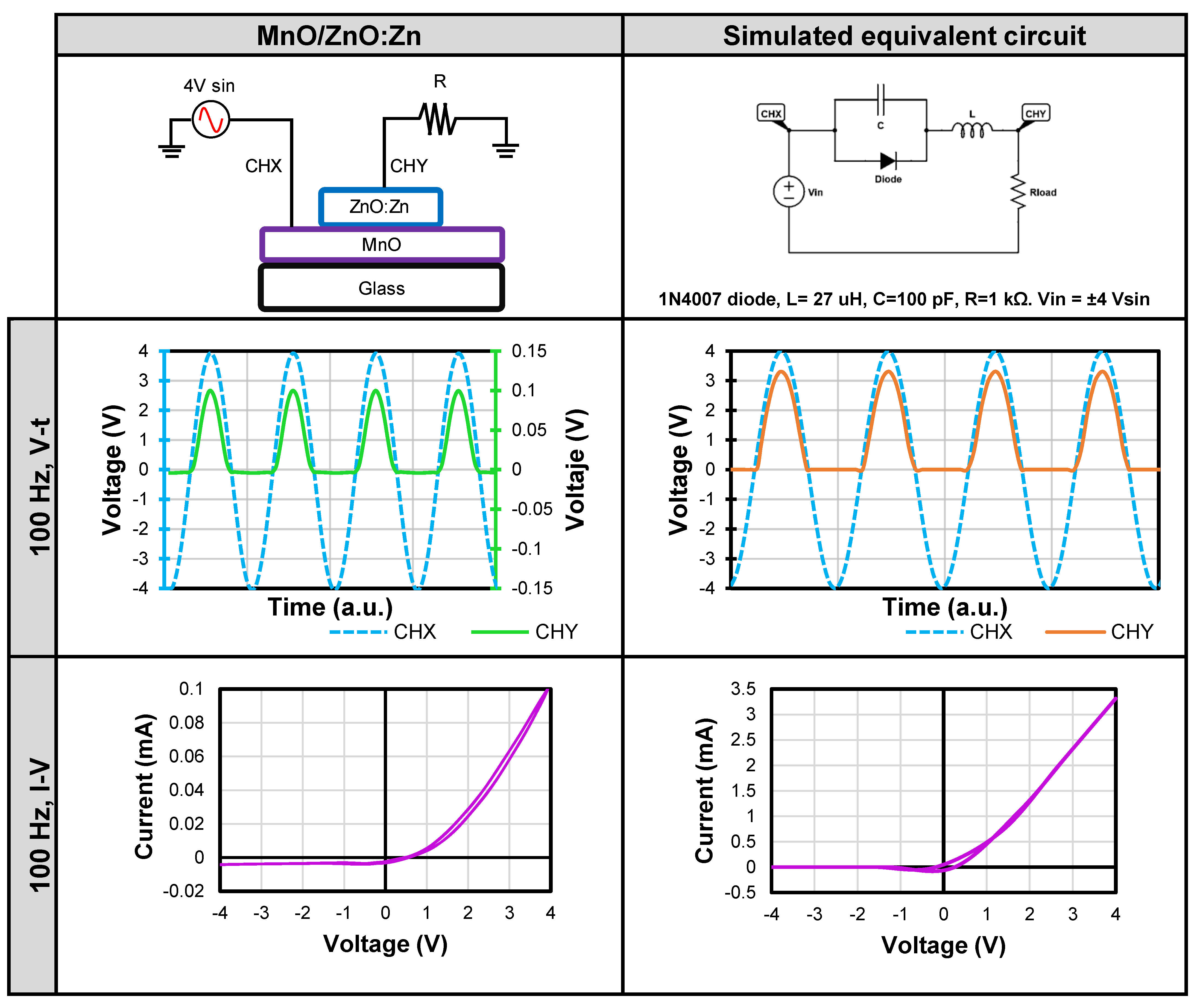
Figure 2a shows the electrical diagram used to measure the MnO/ZnO:Zn heterostructure. A sinusoidal signal was connected in series with a 1 kΩ load resistor designated as R. The voltage signal across the heterostructure was measured directly as CHX, and the equivalent current was monitored by determining the voltage across the load resistor as CHY. The MnO/ZnO:Zn structure acts as a DUT (Device Under Test) in which we know the input and output, and the inside can be modelled with an equivalent circuit in Figure 2b.
3. Results and Discussion
3.1. Average Thickness of the Films
As is well known, the PVD sputtering technique allows for a fine control of the thickness in the synthesis process. With the purpose of corroborate the measurements made by the equipment, a profilometer is used in each set of samples using a step made with Kapton® tape before each deposition.
The thickness average was 116.9 ± 8.4 nm for Mn and 107.1 ± 9.8 nm for ZnO:Zn at the sputtering conditions described above. These results are consistent with the information that the sputtering thickness monitor (Inficon SQM-160) exhibits at the synthesis.
3.2. XRD
The XRDP of the MnGl and ZnGl films are shown in Figure 3. The MnGl diffraction pattern shows two peaks, first the peak at 34.448° corresponds to MnO cubic (111) phase and according to the ICDD #98-065-7311 crystallographic chart. The second peak was observed at 42.378°, which is related to the cubic (101) Mn phase (ICDD #00-017-0910). From this characterisation, two main statements can be established: 1) MnO films grow with a preferential orientation of the crystals at (111). 2) It is possible to observe a minimal quantity of metallic Mn indicating that, during the sputtering process, the deposited Mn was not fully oxidised and implies the presence of Mn as conglomerates, and it can be described as a MnO:Mn film at the defined synthesis conditions.
The XRDP for the ZnGl film reveals only one peak at 34.133° with a high preferential orientation and it corresponds to the plane (002) of ZnO, according with the ICDD #00-036-1451 chart. Structural parameters were calculated using Equation (1) and (2) and the results are presented in Table 1.
In a sputtering and co-sputtering process, the deposition of the film is affected several parameters such as pressure, power, and gas flux which can provoke stress and defects, altering the stability of the lattice, more so, in the case of the ZnO:Zn. To assess the stress in the as-obtained films, Equation (2) was used.
The strain (ε) results indicate that there are tensile stresses in the perpendicular direction to the (002) plane of ZnO and compression in the parallel direction to the plane of the samples. This deformation is associated to interstitial Zn (Zni), in which the atom of Zn has a radius of 137 pm and is introduced to the ZnO lattice in the co-sputtering process [35,36,37]. Zni generates an increase in the interplanar distance, which produces defects, stress and strain in the lattice. This inclusion can be linked to an increase in electrical conductivity as the film can be electrically measured (Appendix A); as is known pure ZnO films display dielectric behaviour whereas the ZnO:Zn system can present an important resistivity decrease [38,39,40].
The MnO films presents almost no strain and is conforming to the glass substrate.
Conditions for bilayer thin-films growth of semiconductors (in this case ZnO:Zn on top of MnO) requires that both materials have a close interplanar distance as to avoid generating interfacial defects. For this reason, the parameter Δd/d between top and bottom layers were calculated as follows [41]:
In this equation, d is the interplanar distance from the diffraction patterns for MnO (bottom) and ZnO:Zn (top) respectively. The mismatch is presented on Table 2.
Table 2 displays the differences involving the semiconductor films deposited by PVD sputtering. The Δd/dMnO percentage of the synthesized heterostructure is 0.846%. The relation Δd/d must be less than 1% [41] to assure a good coupling between the lattices of the materials and to reduce the probability of defects in the interface. The proposed MnO/ZnO:Zn heterostructure meets the requirement for the bilayer and in consequence, is a good candidate for stable memristive systems.
3.3. SEM Micrographs and EDS Analysis
For a morphological analysis of the surfaces of the samples, SEM micrographs were obtained at x10,000 and 5 kV, for both the MnO (MnGl) and ZnO:Zn (ZnGl) layers. Figure 4 shows the surface of the samples in a) and b) respectively. The Mn deposition on glass is uniform and almost no defects are observed. The MnO film has a characteristic mirror-like finish on glass and when the top ZnO:Zn film is applied, no further oxidation is detected in the original film which functions as a passivation layer [42]. Figure 4b shows the ZnO:Zn on glass where a labyrinth pattern can be detected [15]. The layer is transparent as already known in ZnO films, only with a certain tinted blue hue for the ZnO:Zn.
The c) and d) present the EDS analysis of MnO and ZnO:Zn respectively, where the materials of each film are present as main elements, and no other atom is found aside of C.
3.4. Frequency Adaptive Signal Processing
To identify the adaptive behaviour of the MnO/ZnO:Zn, a bilayer structure was produced with the two-stage synthesis procedure described before.
The interface operates under a dynamical polarization (time response), having both resistive and reactive (capacitive and inductive) impedance in the Space-Charge (SC) region. Therefore, to evaluate the technological capabilities of the MnO/ZnO:Zn heterostructure, the SC region of the heterojunction is analysed as a transfer function which is defined as: the ratio between the output and input signals. This is used for analysis of linear systems in electronics and control theory [22].
Under the measurement technique shown in Figure 2, the dynamical behaviour of the MnO/ZnO:Zn structure can represent the correlation between the transfer function and the corresponding I-V characteristics to reveal internal states under specific operating conditions (change in frequency in this case).
The transient activation of states is explained to give a qualitative idea of the transport mechanisms involved in operating the MnO/ZnO:Zn heterojunction. The input is a sinusoidal signal of 4 V for each cycle and is the condition for the reproducible and repeatable states. At 4.8 V the potential barrier is broken, and it permanently loses the rectifying behaviour.
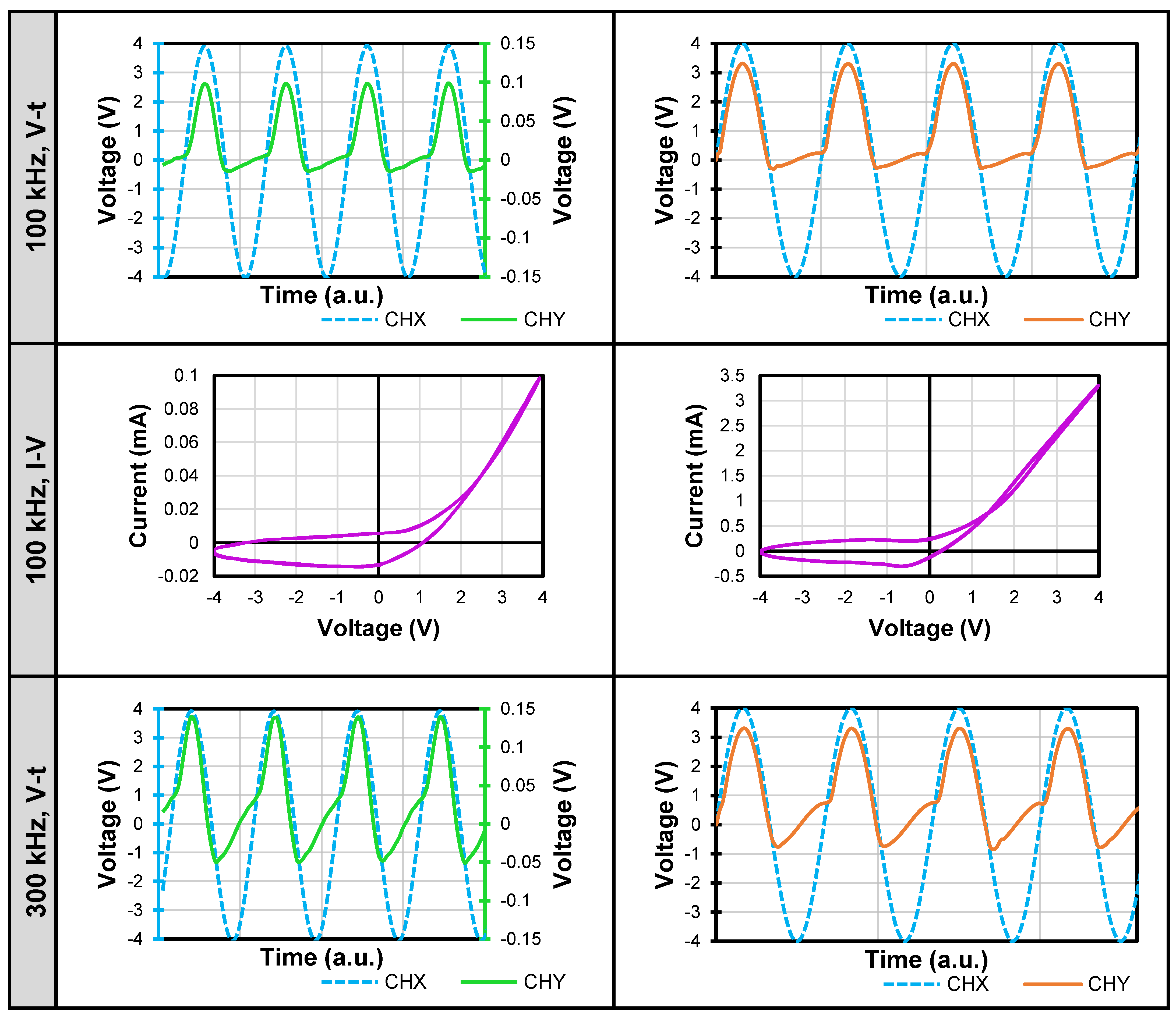
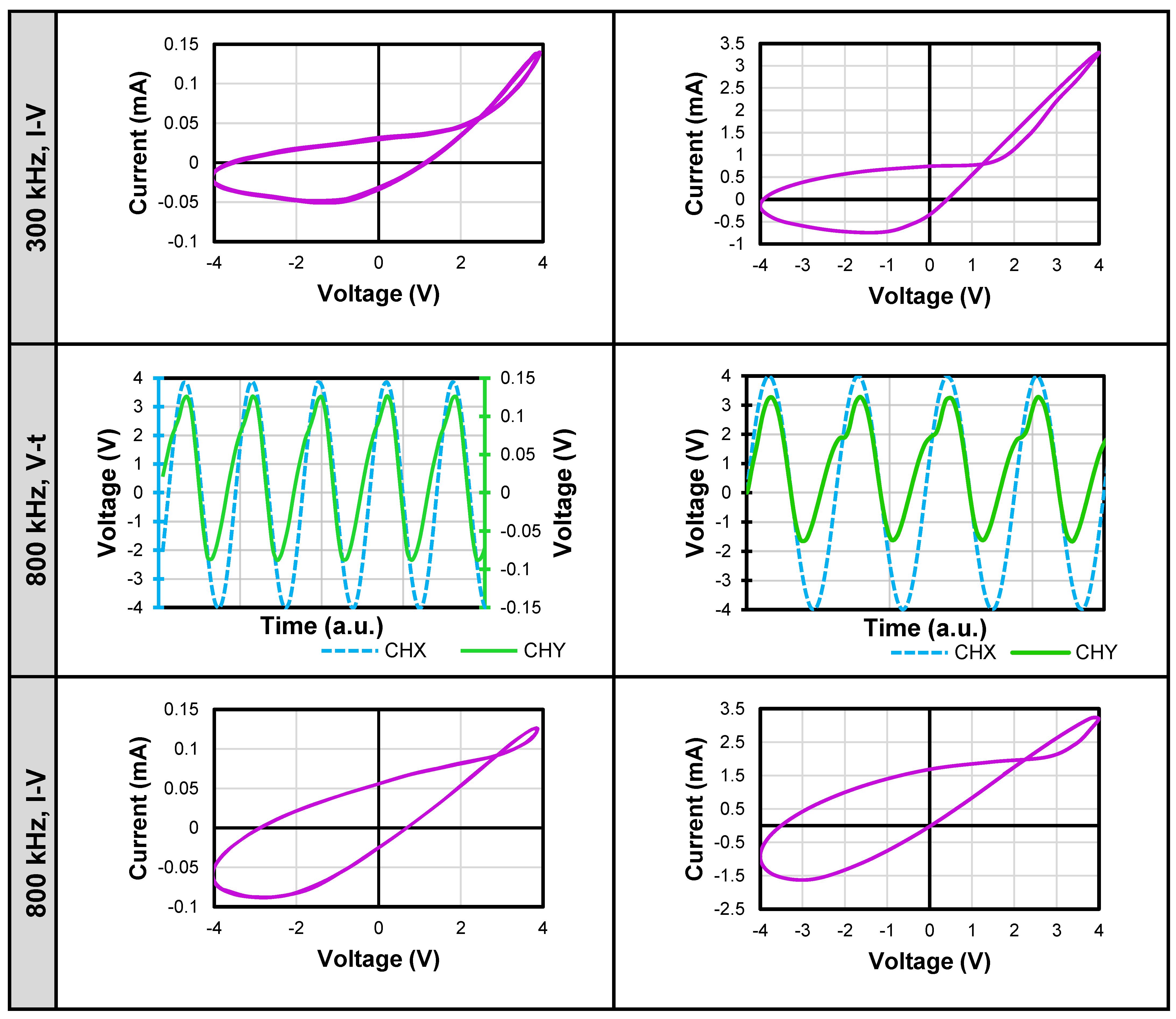
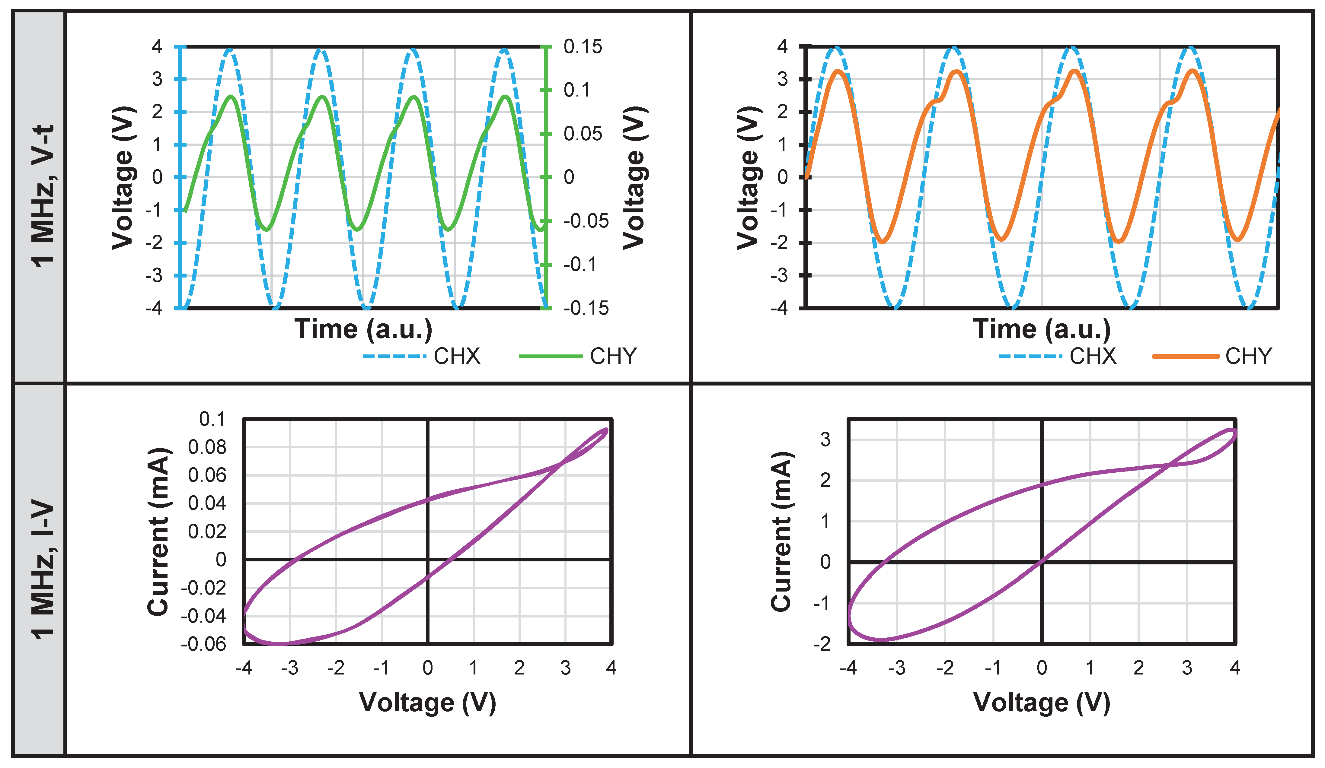
The time-response signals, I-V curves and equivalent circuit with the proposed contribution of each element are showed in Figure 5. The following is an analysis of the performance at different test frequencies, from 100 Hz to 1 MHz.
A barrier is formed at the interface of MnO/ZnO:Zn. This heterojunction behaves as a diode (half wave rectifier) at 100 Hz to 10 kHz. For 100 kHz and 1 MHz the rectifying behaviour changes due to the rise of the frequency and the states reflect a transformation of the signal. The space charge region increases as the frequency rises. The hysteresis of the I-V curves is directly related to this change. The behaviour in each frequency is explained in detail to understand the frequency adaptive signal processing of the device.
At 100 Hz a rectifying and resistive switching state is present at voltages above 1 V. The time response signal of forward bias rectification and the I-V curve confirms it. The origin of the rectification is through the interface between the MnO and ZnO:Zn layers, where a certain number of electrons and holes have flowed and are responsible of the electrical field of the space charge region. Therefore, this resistive switching state can be explained by Space-Charge Limited Currents (SCLC), where charge trapping develops and the heterostructure has slightly changed from a high resistance state to a low resistance state in a forward-bias condition. From 100 Hz to almost 100 kHz the signal behaves in a very similar way to a rectification only state.
With 100 kHz, the capacitive rectifying state is extended from -4V to 4V, where the velocity of injected carriers is lower than the velocity of charge trapping. It shows a response for the reverse bias region (negative cycle) and is reflected as a broadness in the I-V curve in the same voltage region. The transient storing of electron and hole carriers increases around the interface and an additional charge trapping also occurs in the SC. Under this transient condition, the SC region is extended (the electric field reduces) and a random distribution of carriers in the ZnO:Zn region outside the interface is created, which can be responsible of the slowly ionization of defects. Hence, the I-V curve exhibits a hysteresis phenomenon.
For 300 kHz, the rectification effect is almost gone. A crossing is observed in the hysteresis of the curve. This phenomenon is called pinched hysteresis. For the heterojunction, the pinched response is shifted and asymmetric, which correlates with so-called imperfect memristors with a non-zero crossing I-V hysteresis [10,12,43].
At 800 kHz and 1 MHz, the time-response signal does not deliver a rectifying behaviour anymore. A greater capacitive response than the one at 300 kHz is present, and evident by the delay of the signal in the negative cycle of CHY with respect to CHX. When the signal is rising (negative to positive), the capacitive contributions are greater than the resistive ones. On the contrary, when the signal falls (positive to negative) the contributions are almost purely resistive. The capacitive response can be correlated to an increase in the SC region where the holes are filled with more velocity given the higher frequency of the state which are also illustrated in the wider hysteresis of the I-V curve; this capacitive response has been studied separately in other work for a similar structure [44]. At Appendix B, Figure B1 presents the comparison of the V-t and I-V curves of a simulated circuit vs the MnO/ZnO:Zn heterostructure for further analysis of the equivalent circuit.
Finally, the heterojunction does not degrade with the changes in frequency and the states are repeatable over the spectrum of 100 Hz – 1 MHz (meaning that, for example, a jump from 1 MHz to 100 Hz, does deliver the same signal seen in each state). Both the external stimulus of the frequency, and the stable and repeatable signals of each state, allows us to determine that the MnO/ZnO:Zn heterostructure can be deemed as a first approach to future sustainable frequency adaptive memristive systems.
4. Conclusions
In this work, the morphological, structural, and electrical properties of MnO and ZnO:Zn thin films obtained by Sputtering and Co-Sputtering, respectively, are presented. The XRD data, shows that for the MnGl sample, a MnO phase with high preferential orientation in (111) is deposited at the conditions described close to the desired 100 nm. The film conforms to the glass substrate without adhesion problems. Some residual metallic Mn is presumed to be left that could be present as conglomerates, and it can be described as a MnO:Mn film. For the co-sputtered ZnO:Zn film, the growth of the film is preferential towards the (002) plane of the ZnO and the doped Zn atoms are introduced in the hexagonal lattice as interstitial Zn (Zni). These interstitial sites add a characteristic improvement of the conductive behaviour for the ZnO:Zn layer in comparison to pure ZnO films which are non-conductive. This electrical property can be exploited for future devices in which conductive, transparent, and easy to deposit ZnO films could be of use for future memristive applications and for green electronics. The SEM micrographs show a homogeneous surface for both the MnO and ZnO:Zn and the EDS analysis proves the presence of each material with oxygen for the TMO’s.
The electrical response was evaluated using an oscilloscope and a signal generator, to observe the signals in time and the I-V curves at the MnO/ZnO:Zn heterojunction as well as an equivalent circuit comparison in order to explain the electronic circuit behaviour. The performance of the device applying frequencies in the range of 100 Hz to 1 MHz, showed the presence of non-zero crossing I-V hysteresis related to memristive behaviour, and the presence of capacitive effects associated to the MnO/ZnO:Zn interface. It was found that the signal output, at different frequencies, is stable, repeatable, and reproducible as long as the forward/reverse bias voltage does not exceed the ±4 V limit.
The area of adaptive devices is relatively new and has great potential for the development of new applications and technologies to transition from traditional to sustainable electronics. Hopefully, this paper will show how the interaction of MnO and ZnO:Zn oxides can be used in adaptive device applications and use reconfigurability through frequencies and internal states as an option to create new and innovative design schematic with reduced numbers of components/connections in a system.
Author Contributions
Conceptualization, Roberto Baca-Arroyo; Formal analysis, Karen Neri-Espinoza; Investigation, Karen Neri-Espinoza; Methodology, Karen Neri-Espinoza; Project administration, Francisco Gutiérrez-Galicia; Resources, José Andraca-Adame, Francisco Gutiérrez-Galicia and Ramón Peña-Sierra; Supervision, Ramón Peña-Sierra; Writing – original draft, Roberto Baca-Arroyo; Writing – review & editing, Karen Neri-Espinoza, José Andraca-Adame and Miguel Domínguez-Crespo.
Funding
This work was supported by the Consejo Nacional de Humanidades, Ciencia y Tecnologías (CONAHCyT, México) under grant #2777300.
Data Availability Statement
Not Applicable.
Acknowledgments
This work has been possible thanks to the technical support of MSc. Miguel Galván Arellano, MSc. Adolfo Tavira Fuentes and technician Norma Iris González García from Centro de Investigación de Estudios Avanzados del Instituto Politécnico Nacional (CINVESTAV-IPN, México).
Conflicts of Interest
The authors declare no conflict of interest.
Appendix A
Hall Effect Measurement
An electrical characterisation of each layer was made by Hall effect employing the Van der Pauw method using a magnetic field of 0.55 Tesla.
The information from the Hall measurements allows to know the carrier density, mobility, and resistivity of each film. In the ZnO:Zn sample, the Zn incorporation decreases the resistivity and can be measured in comparison to a ZnO film at the same conditions of synthesis [39]. Table A1 indicates the values obtained.

Table A1.
Parameters obtained from Hall measurements for the MnGl and ZnGl samples.
| Sample | Type | Carrier Density (cm-3) | Mobility (cm2/V-s) | Resistivity (Ω-cm) |
|---|---|---|---|---|
| MnGl | p | 3.40x10²¹ | 0.00762 | 0.2385 |
| ZnGl | n | 3.00x10¹⁶ | 9.2182 | 24.6547 |
The difference in semiconductor types for each film can be seen from the results of Table A1. The structure can take advantage of the p-n heterojunction type for a reconfigurable device. For the MnO layer, the main carriers will be the holes (h+) acting as acceptors and for the ZnO:Zn layer, the carriers will be the electrons (e-) acting as donors.
Appendix B
Simulation of Equivalent Circuit
The comparison between the measured MnO/ZnO:Zn structure and the simulated equivalent circuit with SPICE (Simulation Program with Integrated Circuit Emphasis) is shown in Figure A1. The V-t and I-V curves are similar, and the main change is the intensity of the signals as the simulated signals show a minor attenuation in voltage and current. This circuit analogy allows us to observe what the behaviour of the interface between MnO and ZnO:Zn may be like with passive and active elements.
Figure A1.
Comparison of the V-t and I-V curves of the simulated circuit in SPICE versus the MnO/ZnO:Zn response.
Figure A1.
Comparison of the V-t and I-V curves of the simulated circuit in SPICE versus the MnO/ZnO:Zn response.
References
- Hamilton, K. E.; Schuman, C. D.; Young, S. R.; Bennink, R. S.; Imam, N.; Humble, T. S. Accelerating Scientific Computing in the Post-Moore’s Era. ACM Trans. Parallel Comput. 2020, 7. [Google Scholar] [CrossRef]
- Odeh, A. A.; Al-Douri, Y. Metal Oxides in Electronics. In Metal Oxide Powder Technologies; Al-Douri, Y., Ed.; Elsevier, 2020; pp 263–278. [CrossRef]
- Shima, H.; Zhong, N.; Akinaga, H. Switchable Rectifier Built with Pt/ TiOx /Pt Trilayer. Appl. Phys. Lett. 2009, 94, 129–132. [Google Scholar] [CrossRef]
- Choi, H.; Jung, H.; Lee, J.; Yoon, J.; Park, J.; Seong, D. J.; Lee, W.; Hasan, M.; Jung, G. Y.; Hwang, H. An Electrically Modifiable Synapse Array of Resistive Switching Memory. Nanotechnology 2009, 20. [Google Scholar] [CrossRef] [PubMed]
- Ha, S. D.; Aydogdu, G. H.; Viswanath, B.; Ramanathan, S. Electrically-Driven Metal-Insulator Transition with Tunable Threshold Voltage in a VO2-SmNiO3 Heterostructure on Silicon. J. Appl. Phys. 2011, 110, 22–25. [Google Scholar] [CrossRef]
- Ha, S. D.; Ramanathan, S. Adaptive Oxide Electronics: A Review. J. Appl. Phys. 2011, 110. [Google Scholar] [CrossRef]
- Wu, W.; Wang, Z. L. Piezotronics and Piezo-Phototronics for Adaptive Electronics and Optoelectronics. Nat. Rev. Mater. 2016, 1, 1–17. [Google Scholar] [CrossRef]
- Pershin, Y. V.; Di Ventra, M. Memory Effects in Complex Materials and Nanoscale Systems. Adv. Phys. 2011, 60, 145–227. [Google Scholar] [CrossRef]
- Sangwan, V. K.; Hersam, M. C. Neuromorphic Nanoelectronic Materials. Nat. Nanotechnol. 2020, 15, 517–528. [Google Scholar] [CrossRef]
- Sun, B.; Xiao, M.; Zhou, G.; Ren, Z.; Zhou, Y. N.; Wu, Y. A. Non–Zero-Crossing Current-Voltage Hysteresis Behavior in Memristive System. Mater. Today Adv. 2020, 6. [Google Scholar] [CrossRef]
- Xiao, Y.; Jiang, B.; Zhang, Z.; Ke, S.; Jin, Y.; Wen, X.; Ye, C. A Review of Memristor: Material and Structure Design, Device Performance, Applications and Prospects. Sci. Technol. Adv. Mater. 2023, 24. [Google Scholar] [CrossRef]
- Chua, L. If It’s Pinched It’s a Memristor. Semicond. Sci. Technol. 2014, 29. [Google Scholar] [CrossRef]
- Ocampo, O.; Antúnez, E. E.; Agarwal, V. Memristive Devices from Porous Silicon - ZnO/VO2 Nanocomposites. Superlattices Microstruct. 2015, 88, 198–203. [Google Scholar] [CrossRef]
- Martínez, L.; Ocampo, O.; Kumar, Y.; Agarwal, V. ZnO-Porous Silicon Nanocomposite for Possible Memristive Device Fabrication. Nanoscale Res. Lett. 2014, 9, 1–6. [Google Scholar] [CrossRef] [PubMed]
- Martínez, L.; Becerra, D.; Agarwal, V. Dual Layer ZnO Configuration over Nanostructured Porous Silicon Substrate for Enhanced Memristive Switching. Superlattices Microstruct. 2016, 100, 89–96. [Google Scholar] [CrossRef]
- Yarragolla, S.; Hemke, T.; Trieschmann, J.; Mussenbrock, T. Coexistence of Resistive Capacitive and Virtual Inductive Effects in Memristive Devices. 2024, No. Cic.
- Leng, Y. B.; Zhang, Y. Q.; Lv, Z.; Wang, J.; Xie, T.; Zhu, S.; Qin, J.; Xu, R.; Zhou, Y.; Han, S. T. Recent Progress in Multiterminal Memristors for Neuromorphic Applications. Advanced Electronic Materials. 2023. [CrossRef]
- Saraf, S.; Markovich, M.; Vincent, T.; Rechter, R.; Rothschild, A. Memory Diodes with Nonzero Crossing. Appl. Phys. Lett. 2013, 102. [Google Scholar] [CrossRef]
- Ahir, N. A.; Takaloo, A. V.; Nirmal, K. A.; Kundale, S. S.; Chougale, M. Y.; Bae, J.; Kim, D. kee; Dongale, T. D. Capacitive Coupled Non-Zero I–V and Type-II Memristive Properties of the NiFe2O4–TiO2 Nanocomposite. Materials Science in Semiconductor Processing. 2021. [CrossRef]
- Hu, Q.; Abbas, H.; Kang, T. S.; Lee, T. S.; Lee, N. J.; Park, M. R.; Yoon, T. S.; Kim, J.; Kang, C. J. Forming-Free Resistive Switching Characteristics in Manganese Oxide and Hafnium Oxide Devices. Jpn. J. Appl. Phys. 2019, 58. [Google Scholar] [CrossRef]
- Zhang, S.; Long, S.; Guan, W.; Liu, Q.; Wang, Q.; Liu, M. Resistive Switching Characteristics of MnOx-Based ReRAM. J. Phys. D. Appl. Phys. 2009, 42. [Google Scholar] [CrossRef]
- Chang, W. Y.; Lai, Y. C.; Wu, T. B.; Wang, S. F.; Chen, F.; Tsai, M. J. Unipolar Resistive Switching Characteristics of ZnO Thin Films for Nonvolatile Memory Applications. Appl. Phys. Lett. 2008, 92, 1–4. [Google Scholar] [CrossRef]
- Xu, J.; Zhao, X.; Zhao, X.; Wang, Z.; Tang, Q.; Xu, H.; Liu, Y. Memristors with Biomaterials for Biorealistic Neuromorphic Applications. Small Sci. 2022, 2. [Google Scholar] [CrossRef]
- Shangguan, E.; Wang, L.; Wang, Y.; Li, L.; Chen, M.; Qi, J.; Wu, C.; Wang, M.; Li, Q.; Gao, S.; Li, J. Recycling of Zinc−Carbon Batteries into MnO/ZnO/C to Fabricate Sustainable Cathodes for Rechargeable Zinc-Ion Batteries. ChemSusChem 2022, e202200720. [Google Scholar] [CrossRef]
- Electronics Can Be More Sustainable. Nat. Mater. 2023, 22 (11), 1273. [CrossRef]
- Baca-Arroyo, R. Reconfiguration Using Bio-Inspired Conduction Mode of Field-Effect Transistors toward the Creation of Recyclable Devices. Electron. 2023, 12. [Google Scholar] [CrossRef]
- Sze, S.; Ng, K. K. Physics of Semiconductor Devices, 3rd Ed.; John Wiley & Sons, 2007.
- Frey, C. E.; Kwok, F.; Gonzáles-Flores, D.; Ohms, J.; Cooley, K. A.; Dau, H.; Zaharieva, I.; Walter, T. N.; Simchi, H.; Mohney, S. E.; Kurz, P. Evaporated Manganese Films as a Starting Point for the Preparation of Thin-Layer MnO: X Water-Oxidation Anodes. Sustain. Energy Fuels 2017, 1, 1162–1170. [Google Scholar] [CrossRef]
- Jamil, H.; Khaleeq-Ur-Rahman, M.; Dildar, I. M.; Shaukat, S. Structural and Optical Properties of Manganese Oxide Thin Films Deposited by Pulsed Laser Deposition at Different Substrate Temperatures. Laser Phys. 2017, 27. [Google Scholar] [CrossRef]
- Broughton, J. N.; Brett, M. J. Investigation of Thin Sputtered Mn Films for Electrochemical Capacitors. Electrochim. Acta 2004, 49, 4439–4446. [Google Scholar] [CrossRef]
- Ai, R.; Zhang, T.; Guo, H.; Luo, W.; Liu, X. Multilevel Resistive Switching and Synaptic Behaviors in MnO-Based Memristor. Curr. Appl. Phys. 2022, 41, 123–130. [Google Scholar] [CrossRef]
- Mao, S.; Sun, B.; Yang, Y.; Wang, J.; Zhao, H.; Zhao, Y. α-MnO2 Nanorods-Based Memristors with Nonvolatile Resistive Switching Behavior. Ceram. Int. 2022, 48, 32860–32866. [Google Scholar] [CrossRef]
- Amador, L. I. J.; Arellano, M. G.; Adame, J. A. A.; Paredes, G. R.; Sierra, R. P. Electrical, Optical and Magnetoresistive Behavior of Nanostructured ZnO : Cu Thin Films Deposited by Sputtering. J. Mater. Sci. Mater. Electron. 2018, 0. [Google Scholar] [CrossRef]
- Neri-Espinoza, K. A.; Baca-Arroyo, R.; Andraca-Adame, J. A.; Pena-Sierra, R. Interface Phenomena in MnxOy/ZnO) Thin Films for Oxide Electronics. 2019 16th Int. Conf. Electr. Eng. Comput. Sci. Autom. Control. CCE 2019 2019, 3–7. [Google Scholar] [CrossRef]
- Janotti, A.; Van De Walle, C. G. Fundamentals of Zinc Oxide as a Semiconductor. Reports Prog. Phys. 2009, 72. [Google Scholar] [CrossRef]
- Coleman, V. A.; Jagadish, C. Basic Properties and Applications of ZnO. Zinc Oxide Bulk, Thin Film. Nanostructures. 2006, 1–20. [CrossRef]
- Walukiewicz, W. Defect Formation and Diffusion in Heavily Doped Semiconductors. Phys. Rev. B 1994, 50, 5221–5225. [Google Scholar] [CrossRef] [PubMed]
- Wang, X. J.; Vlasenko, L. S.; Pearton, S. J.; Chen, W. M.; Buyanova, I. A. Oxygen and Zinc Vacancies in As-Grown ZnO Single Crystals. J. Phys. D. Appl. Phys. 2009, 42. [Google Scholar] [CrossRef]
- Vasquez-A. , M. A.; O., G.; Baca-Arroyo, R.; Andraca-Adame, J. A.; Romero-Paredes, G.; Peña-Sierra, R. Study of the Properties of ZnO:Zn Thin Films Obtained from ZnO/Zn/ZnO Structure Deposited by DC Sputtering. J. Nanosci. Nanotechnol. 2013, 12, 9234–9237. [Google Scholar] [CrossRef]
- Oba, F.; Choi, M.; Togo, A.; Tanaka, I. Point Defects in ZnO: An Approach from First Principles. Sci. Technol. Adv. Mater. 2011, 12. [Google Scholar] [CrossRef] [PubMed]
- Roblin, P.; Rohdin, H. High-Speed Heterostructure Devices. From Device Concepts to Circuit Modeling, 1st Ed. ed; Cambridge University Press: New York, 2002. [Google Scholar]
- Yang, M.; Li, K.; Xiao, L. Zinc Oxide/Manganese Oxide Hybrid Nanostructure for Electrode and Asymmetric Supercapacitor with Long-Term Cyclic Life. Mater. Sci. Eng. B Solid-State Mater. Adv. Technol. 2021, 269. 115173. [Google Scholar] [CrossRef]
- Biolek, D.; Biolek, Z.; Biolkova, V. Pinched Hysteretic Loops of Ideal Memristors, Memcapacitors and Meminductors Must Be “Self-Crossing. ” Electron. Lett. 2011, 47, 1385–1387. [Google Scholar] [CrossRef]
- Neri-Espinoza, K. A.; Domínguez-Crespo, M. A.; Andraca-Adame, J. A.; Peña-Sierra, R. Evaluation of the Electrical Properties of MnO/ZnO:Zn Thin-Films for Potential Applications in Solid-State Supercapacitors. 2023, 1–6. [CrossRef]
Figure 1.
a) Photograph of a complete MnO/ZnO Heterostructure, b) Cross-sectional diagram of the structure, indicating the thickness of the as-prepared films, c) Area of deposition showing the stainless-steel mask to define each material.
Figure 1.
a) Photograph of a complete MnO/ZnO Heterostructure, b) Cross-sectional diagram of the structure, indicating the thickness of the as-prepared films, c) Area of deposition showing the stainless-steel mask to define each material.
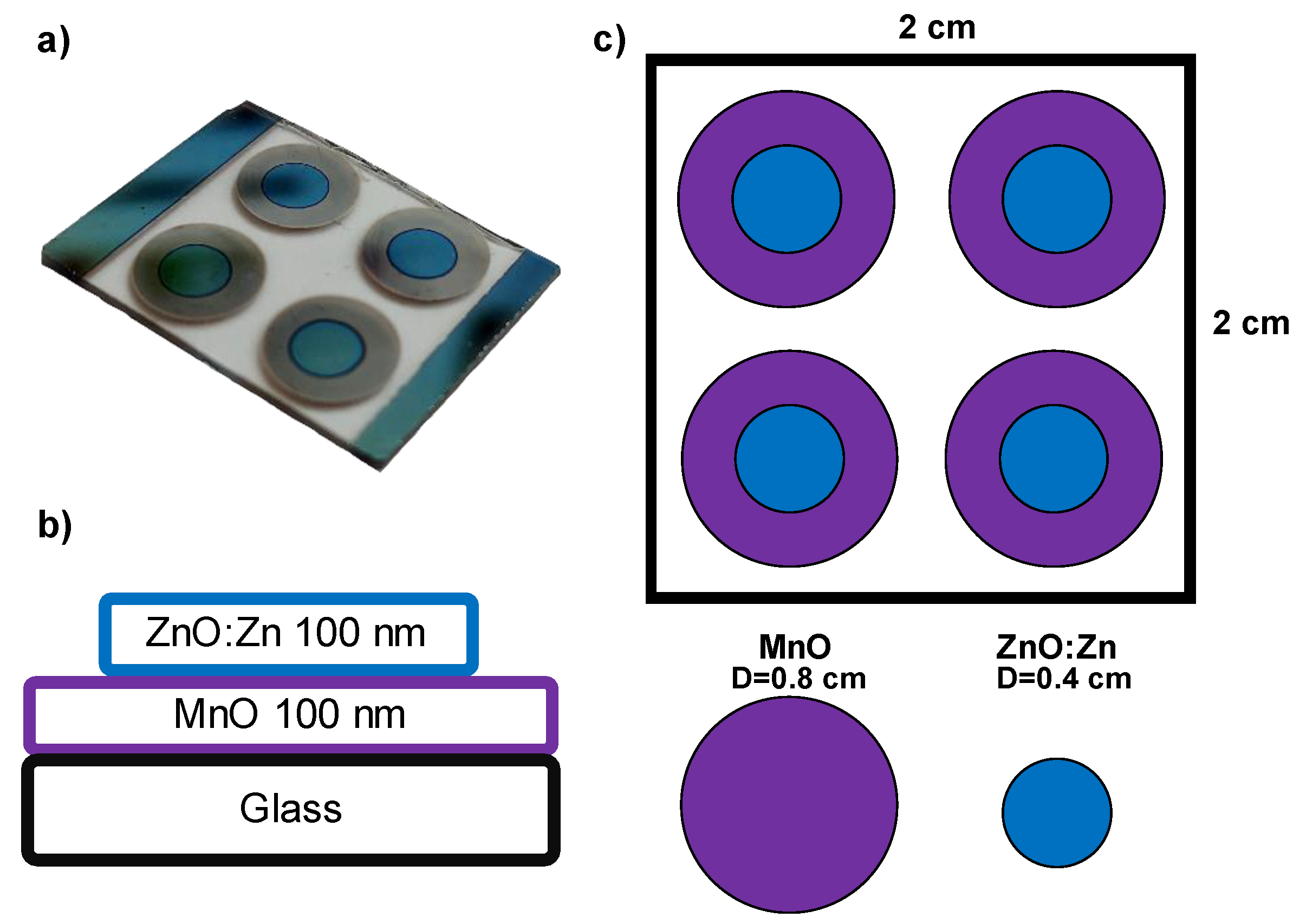
Figure 2.
a) Electrical diagram proposed to evaluate the MnO/ZnO:Zn heterostructure. CHX and CHY are the channels of the oscilloscope. b) The heterostructure is a DUT where, with the analysis of the signals obtained with the oscilloscope, the adaptive behaviour dependant of the frequency can be related to an analogy of a circuit.
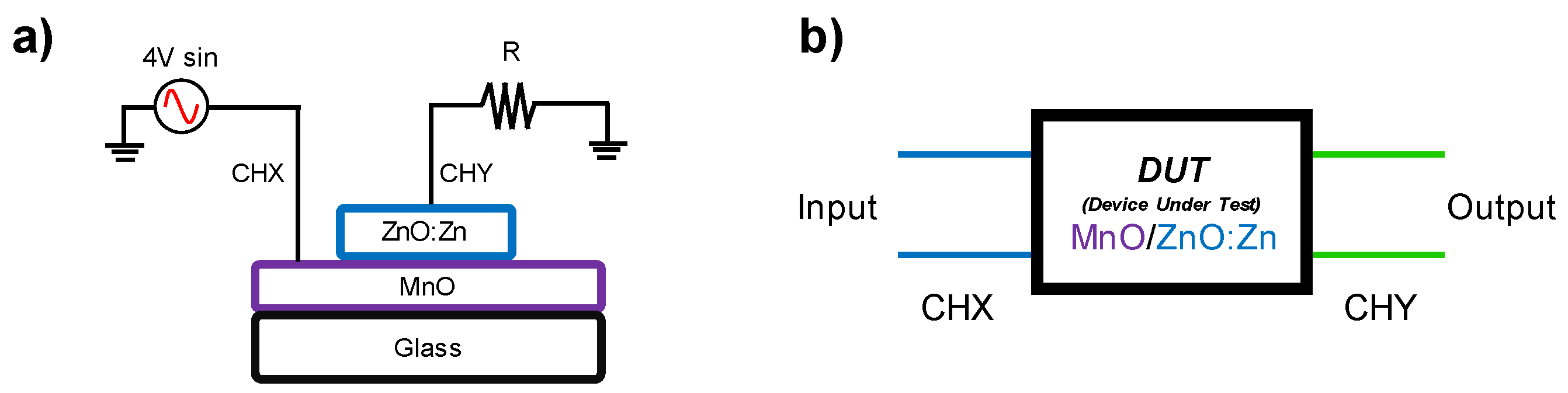
Figure 3.
Diffraction patterns for MnGl and ZnGl.
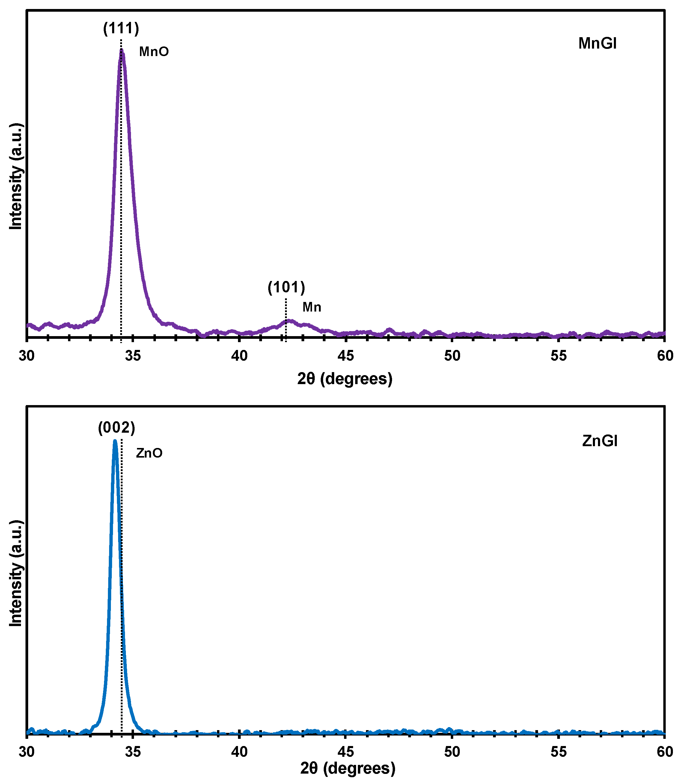
Figure 4.
a) SEM micrograph of the surface of MnO (MnGl) at x10,000, b) SEM micrograph of the surface of ZnO:Zn (ZnGl), c) EDS analysis of MnGl, d) EDS analysis of ZnGl.
Figure 4.
a) SEM micrograph of the surface of MnO (MnGl) at x10,000, b) SEM micrograph of the surface of ZnO:Zn (ZnGl), c) EDS analysis of MnGl, d) EDS analysis of ZnGl.
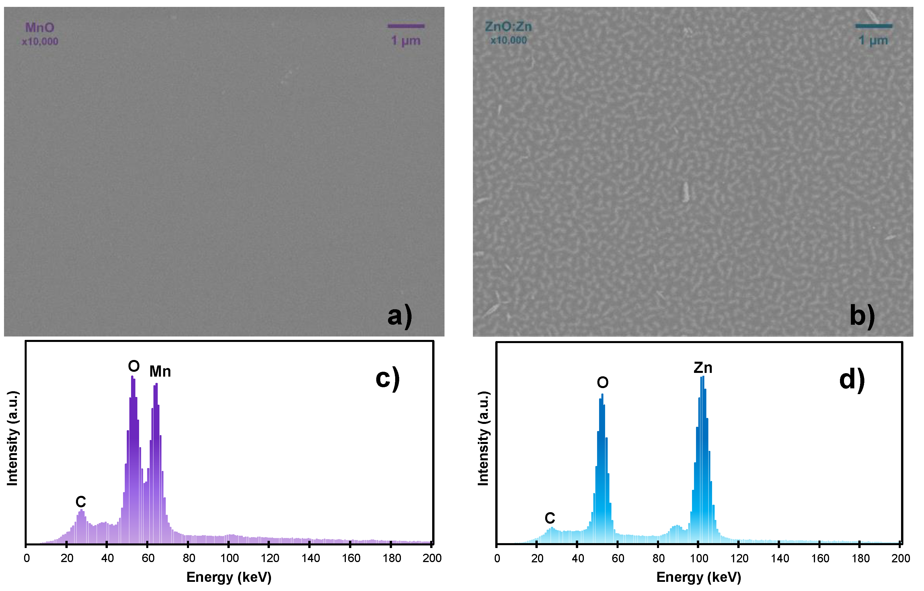
Figure 5.
States of the heterostructure where the time response, I-V curves and equivalent circuit are shown for each frequency (external stimulus). CHX and CHY are visible in the time-response graph, each having a different scale given the attenuation of the output signal (CHY). The I-V curves reveal the evolution of the space charge region at each frequency. The analogy of the circuit is also presented, were the simulation for a 1N4007 diode, L= 27 uH, C=100 pF and Rload= 1 kΩ, shows a similar output signal to the ones of the heterostructure at those frequencies. The states are stable and can be achieved repeatedly under a signal of 4 V or less in the input.
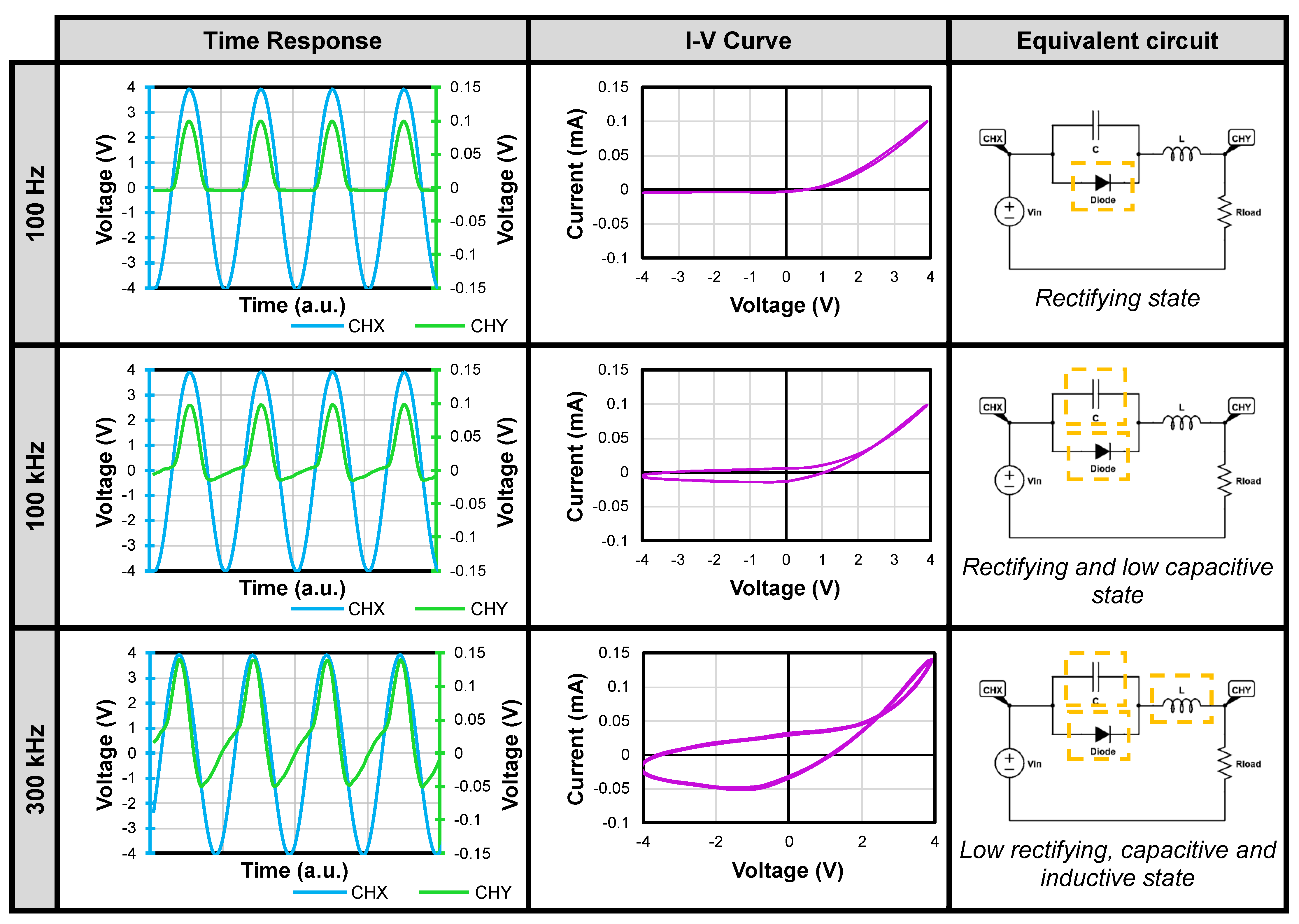
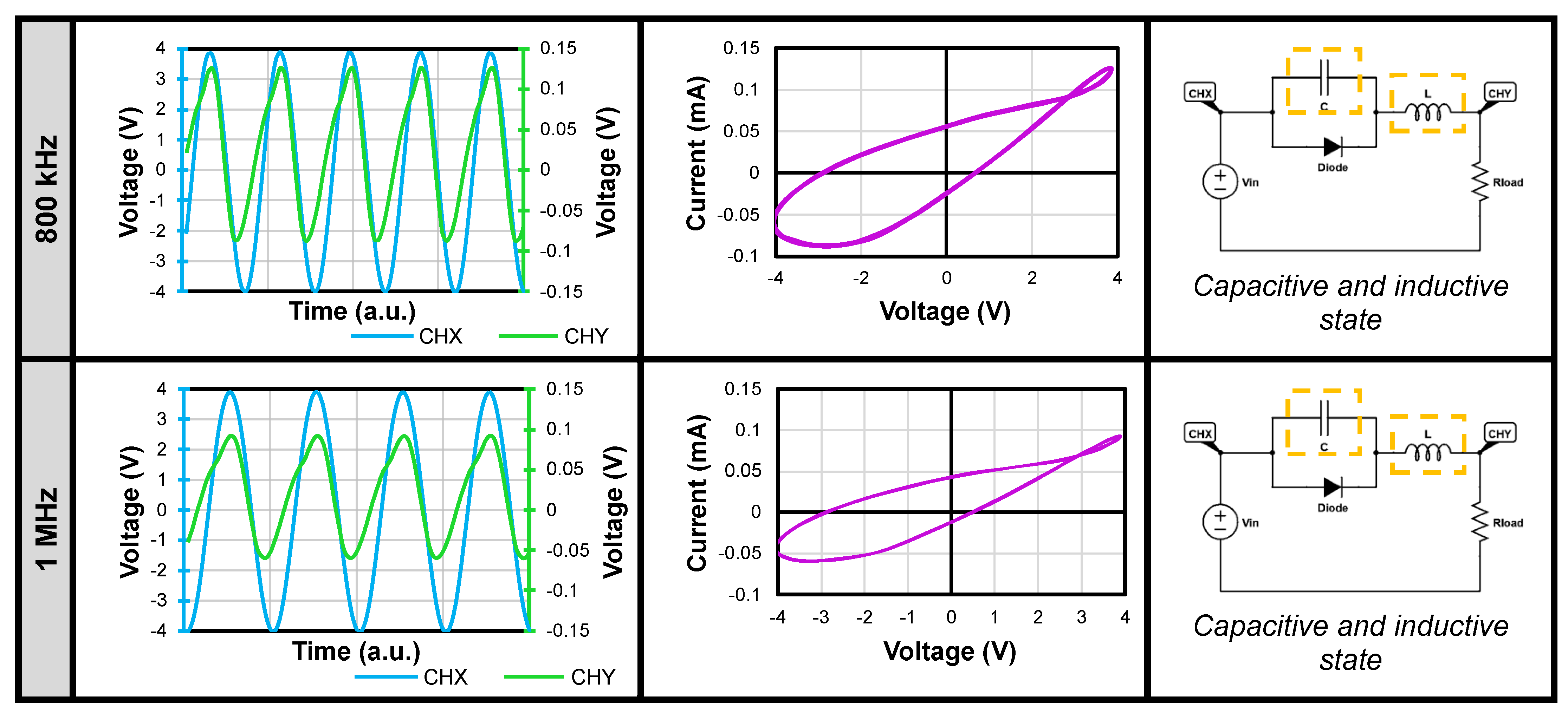
Table 1.
Crystallite size (D), strain (), 2θ (measured θm and reference, θr) and 2θ displacement (Δθ).
Table 1.
Crystallite size (D), strain (), 2θ (measured θm and reference, θr) and 2θ displacement (Δθ).
| Plane | Phase | 2θm (°) | 2θr (°) | Δθ | D (nm) | (%) |
|---|---|---|---|---|---|---|
| (111) | MnO | 34.448 | 34.446 | 0.002 | 10.3 | -80x10-6 |
| (002) | ZnO | 34.133 | 34.422 | -0.289 | 16.14 | -0.77 |
Table 2.
Parameters of interplanar distance (d) for MnO (bottom) and ZnO:Zn (top) films.
| Plane | Layer | d (Å) | Δd/dMnO (%) |
|---|---|---|---|
| (111) | MnO | 2.601 | - |
| (002) | ZnO:Zn | 2.623 | 0.846 |
Disclaimer/Publisher’s Note: The statements, opinions and data contained in all publications are solely those of the individual author(s) and contributor(s) and not of MDPI and/or the editor(s). MDPI and/or the editor(s) disclaim responsibility for any injury to people or property resulting from any ideas, methods, instructions or products referred to in the content. |
© 2024 by the authors. Licensee MDPI, Basel, Switzerland. This article is an open access article distributed under the terms and conditions of the Creative Commons Attribution (CC BY) license (http://creativecommons.org/licenses/by/4.0/).
Copyright: This open access article is published under a Creative Commons CC BY 4.0 license, which permit the free download, distribution, and reuse, provided that the author and preprint are cited in any reuse.


