1. Introduction
Integrated circuits (or logic circuits), constitute a fundamental aspect of the modernized world, catering to the daily needs of millions. The rapidly emerging era of Internet of Things (IoT) only accentuates this claim. As IoT devices increasingly permeate critical sectors, such as healthcare, automotive, and home automation, their security implications cannot be overstated. These devices often handle sensitive data and control systems integral to safety and privacy. The challenges confronting ICs revolve around the considerable expenses associated with circuit design and the initial acquisition of manufacturing equipment. The substantial costs incurred during the design phase render integrated circuit fabrication economically viable only in scenarios involving high-volume production. To address the second challenge, a strategic solution involves the bifurcation of IC design and fabrication processes. In this approach, fabrication is delegated to specialized foundries capable of producing circuits for multiple design companies. This decentralized model not only mitigates the financial burden of individual manufacturing setups but also fosters collaboration and efficiency in the production of integrated circuits. Ultimately, these intricate electronic components continue to drive technological advancements, underscoring their indispensability in contemporary society.
Outsourcing the fabrication of integrated circuits to external entities introduces a heightened susceptibility to forgery, piracy, and unauthorized reproduction, necessitating vigilant measures to mitigate associated risks. The absence of stringent monitoring and direct control over the fabrication process in external companies exposes the vulnerability of intellectual property to potential attacks. A malicious foundry, exploiting this vulnerability, may present a product with compromised IC security as its own, engaging in illegal copying and unauthorized sale under its brand. Such security risks, commonly referred to as subcontractor attacks, pose substantial economic threats to prominent IC design companies. Conversely, perpetrators stand to gain significant financial advantages by compromising designs, compelling designers to create circuits fortified against potential attacks. Striking a delicate balance between outsourcing efficiency and safeguarding intellectual property becomes imperative in navigating the intricate landscape of integrated circuit fabrication.
The paper is organized as follows. A brief overview of some chosen security mechanism for securing logic circuits is presented in
Section 2. The used attack on logic locking using a SAT solver is stated in
Section 3. The results obtained in the experiments are presented in
Section 4. Finally, conclusions and possible way for future research are stated in
Section 5.
2. Logic Circuits and Their Security
Because of these risks, different ways of securing integrated circuits began to emerge. A brief history of logic locking can be found in [
14]. One of the first security methods was the passive protection, which was based on a unique identifier (ID) [
6]. Each circuit contained its own identifier that was physically engraved on it. This protection facilitated the detection of fake products but did not interfere with its production process.
The first active scheme for protecting logic circuits was the generation of identifiers. Each integrated circuit generates a unique identifier during initialization. This identifier remains encrypted. Only the intellectual property holder can activate the circuit using a unique identifier to generate the unlocking key.
A possible extension, which was described in the work [
1], is the use of an identifier that would be integrated within the Finite State Machine (FSM). Only a circuit designer who knows the extended FSM structure can know the key to activate the circuit. Designing active protection of integrated circuits is challenging because different types of overheads (for security as well) increase the price of the product and make it less attractive to the consumer [
2].
To secure logic circuits against the illegal copying the insertion of the so-called key bit inputs using XOR/XNOR gates has been proposed in [
3]. The inserted gates modify (lock) the behavior of the original circuit and only the correct choice of the secret key bits guarantees the equivalent behaviour of the locked circuit to the original circuit.
The use of a set of lookup tables to the circuit such that every path from an input to an output goes through a lookup table was proposed as another locking scheme in [
10]. The process of logic locking performed on a gate-level was automated in [
7], where the authors developed a software in Python, that can be integrated with the existing digital synthesis tools. The method based on the insertion of key gates in the so-called interference mode, proposed in [
8], is claimed to have less hardware overhead, higher speed, and to be more effective against SAT attacks than the existing conventional methods. A provable secure logic locking scheme that can thwart SAT-based attacks was proposed in [
9]. The authors in [
15] propose a generalized method for logic locking that is resistant against SAT attack. The locking scheme with low complexity resistant against the so-called removal attacks was proposed in [
16]. The complexity analysis of the SAT attack on logic locking can be found in [
20]. The logic locking schemes designed on lower levels were proposed in [
11,
12,
13].
In the following we will omit the technical realization of ICs and discuss the logic circuit level only. Before the circuit is activated, it is necessary in the design to think about incorporating the key into the circuit and thus connecting the key bits to the existing logic gates of the circuit, while it is necessary to preserve the required functionality. There are several techniques that use the insertion of key bits into a circuit. They differ in the type of gates for connecting the key bits into the circuit and also in the way these gates are placed. The list of gates used in this work is shown in
Figure 1. We will briefly describe some possible ways of inserting the key into the circuit in the next subsections.
2.1. Inserting Key Bits into a Gate Scheme Using XOR and XNOR Gates
Combinational locking is performed in the most important IC modules by inserting XOR or XNOR gates at selected locations with added checks associated with the key. This technique was proposed in [
3]. With the correct key, the locked circuit behaves equivalently to the unlocked one, i.e.
, where
is the input,
is the key,
represents the output from the unlocked circuit and
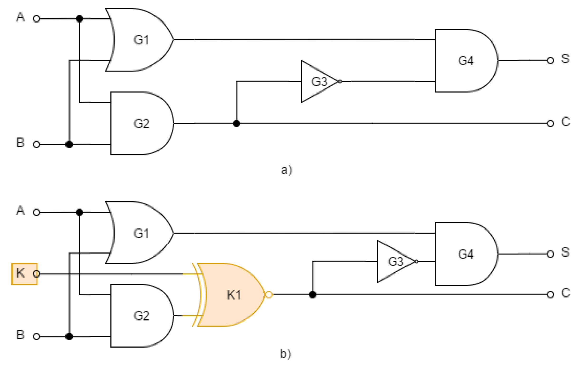
represents the output from the locked circuit. Otherwise, the circuit behaves differently. In
Figure 2 (
b) we can see the combinational locking of the integrated circuit using the XNOR gate.
The security prerequisite of a locked circuit is the uniqueness of the key, i.e. the fulfillment of the following relationship:
The claim says that there must be exactly one key such that for each input of the locked circuit we get the same output as the unlocked one. If this statement does not hold, this expression becomes a Boolean function to find the combination of keys. The length of the key should be long enough to withstand a brute force attack. A key length of at least 80 bits is therefore recommended.
2.1.1. Random Placement of Key Gates
The easiest for inserting key bits into the logic circuit is to choose random location for key gates. The EPIC algorithm [
3] uses the following simple approach to protect the circuit from piracy. Firstly,
k random wires in the circuit marked as
and their corresponding key bits
are chosen. Wires should avoid critical areas and overloaded regions. For each selected wire
, its source is disconnected and either an XOR gate (
) or an XNOR gate (
) is inserted. The choice of XOR or XNOR gate depends on the value of the bit
. If
, an XOR gate is added, otherwise, an XNOR gate is added. Use of identity from
Table 1,
, complicates reverse engineering because the designer or software can replace the selected XOR gate with an XNOR gate and inverter or vice versa.
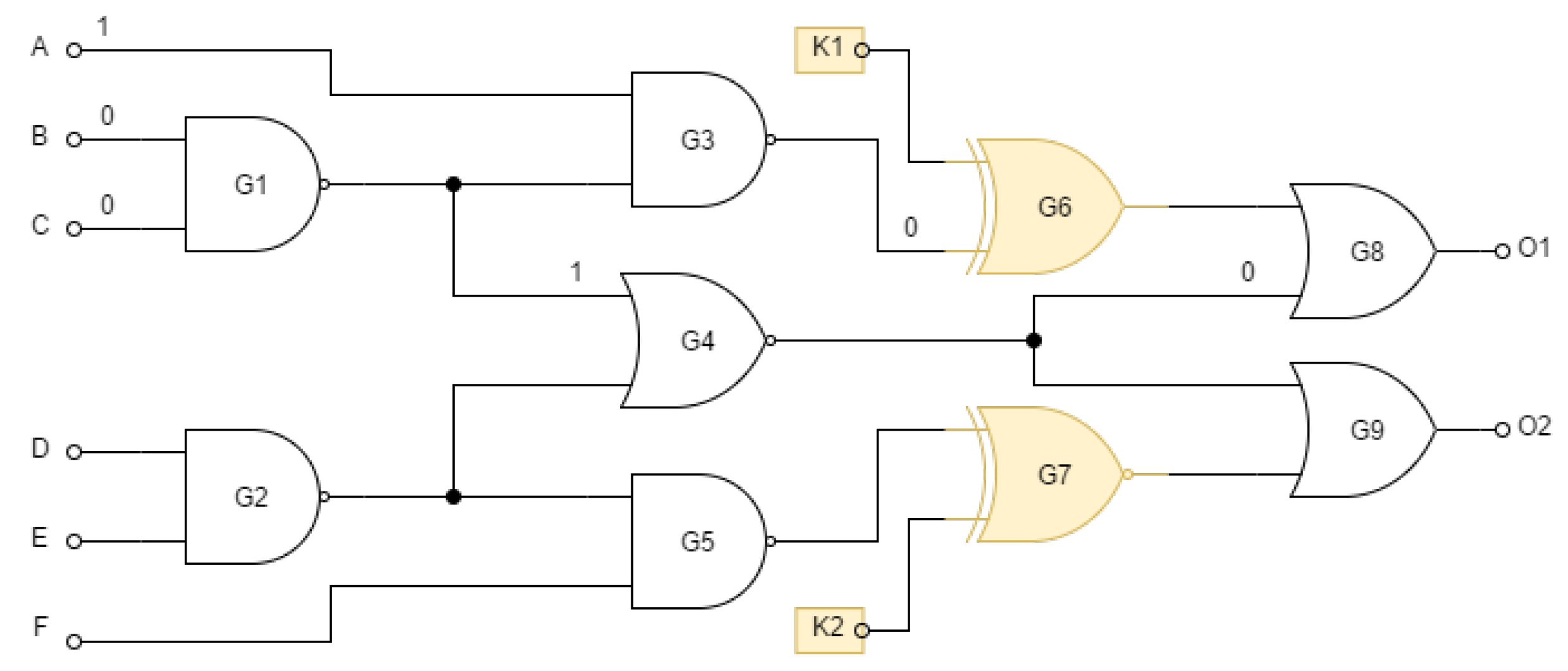
However, random placement of gates is not in general a very secure solution for locking the circuit. The value of an unknown key bit can be determined if it is sensitive to the output without being masked by other key and input bits. If we assume that an attacker knows the layout of the circuit, he can specify an input pattern that will propagate the correct key value to the output. Consider the locked circuit in
Figure 3. The key bit
will be sensitive on the output
if the second value on the gate
is 0 (non-controlling value on the OR gate). This can be achieved by setting the input pattern to
,
, and
. If an attacker has access to the functional circuit, he can use this pattern to find the value of
at the output of
. For example, if the value of
for this pattern then
, otherwise
.
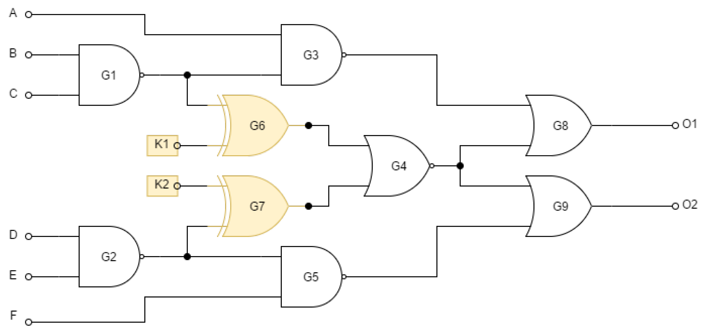
To prevent such attacks, the sensitivity of the keys must be ensured by placing the key gates in such places where the propagation of key bits is possible only if certain conditions are met. In
Figure 4 is a circuit with the same functionality as in the
Figure 3 but with differently positioned key gates. If the attacker wants to propagate the value of one of the keys, then a 0 must be forced on one of the inputs of
. To reach this value, the attacker must control key inputs that are inaccessible. They are stored in a breach-indicating memory inside the structure to prevent attacker access. Thus, propagating the key value to the output is infeasible.
2.1.2. Chained Key Gates
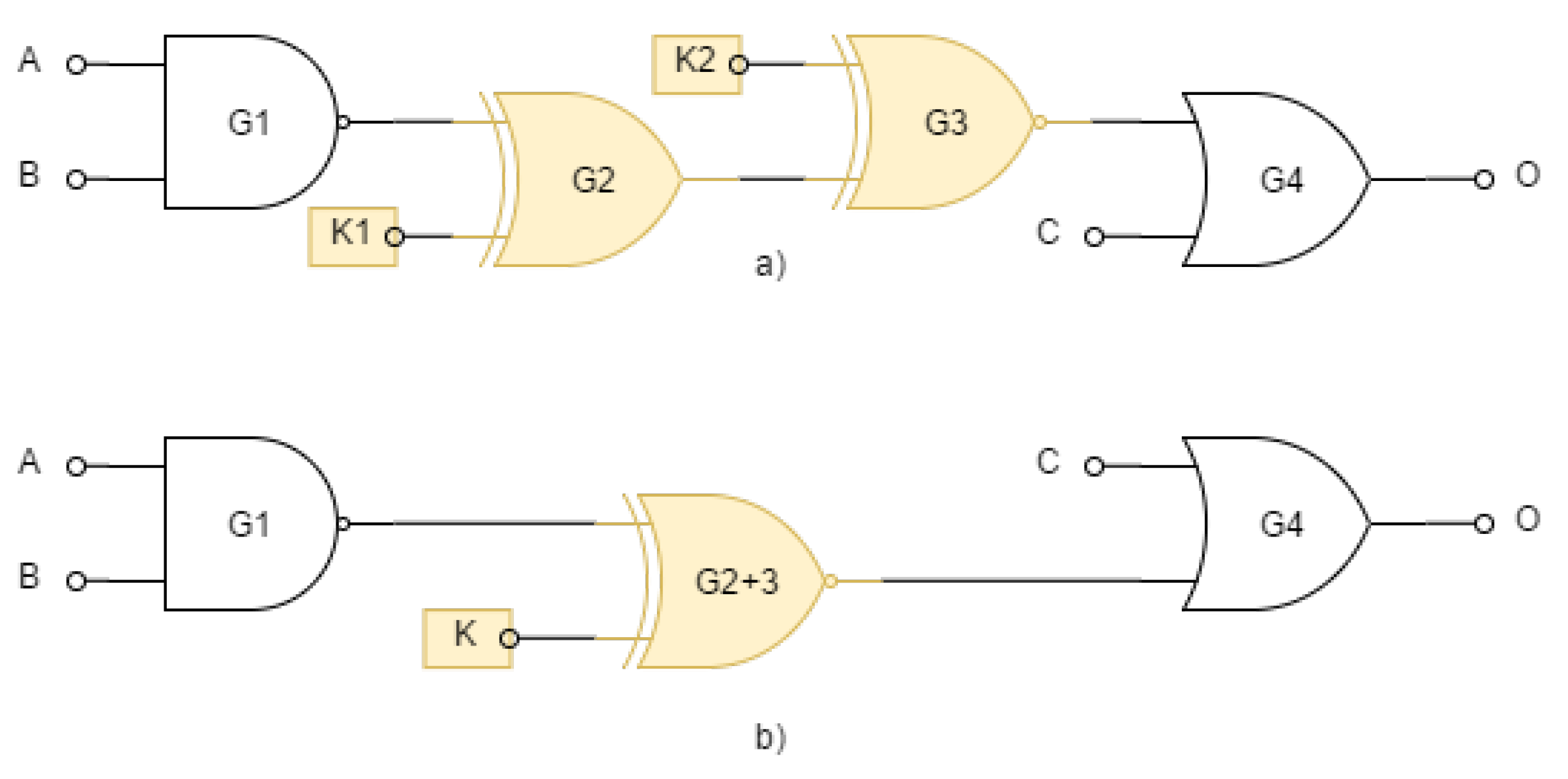
In the case of connecting several key gates one after the other, we speak of chained key gates. Chained key gates reduce the effort for an attacker because they increase the space of valid keys. In the case of n chained gates, the space of valid keys increases from the only one (optimal) to .
In
Figure 5 the attacker replaces the two sequentially running key gates
and
in a) with one marked as
in b). If we succeed in finding the value of the key
K, we would have two suitable solutions for the pair
and
. In that case, the equation (
1) does not hold and the difficulty of the attack is reduced.
There are of course several other techniques for locating key gates. Depending on these techniques, attackers have also developed different approaches to reveal the key bits [
4].
3. Description of the Attack
The locked circuit can be described using the relation among the input bits, key bits, and the output bits where is the set of Boolean values, vector represents M primary inputs of the circuits, vector represents the key bits, and vector denotes the N primary output bits. Relation is equivalent to the input/output relation of the unlocked circuit if the correct key value is set.
Relation , i.e. the circuit layout including the key bits, can also be represented by a conjunctive normal form (CNF) with Boolean variables . This representation forms the basis of the attack described below.
It is assumed that the attacker has the layout of the circuit (so-called netlist) and has its unlocked version, so he can observe the correct behavior of the circuit for arbitrary inputs. We will model this observation using the function .
The goal of the attacker is to find such a key , which would satisfy the following equivalence for all input patterns .
In this work, we consider the type of attack in which the attacker has vectors of input values and the corresponding vectors of output values . The behavior of the locked circuit, in other words the relationship between known input and output bits and unknown key bits can be described using a Boolean formula of the form
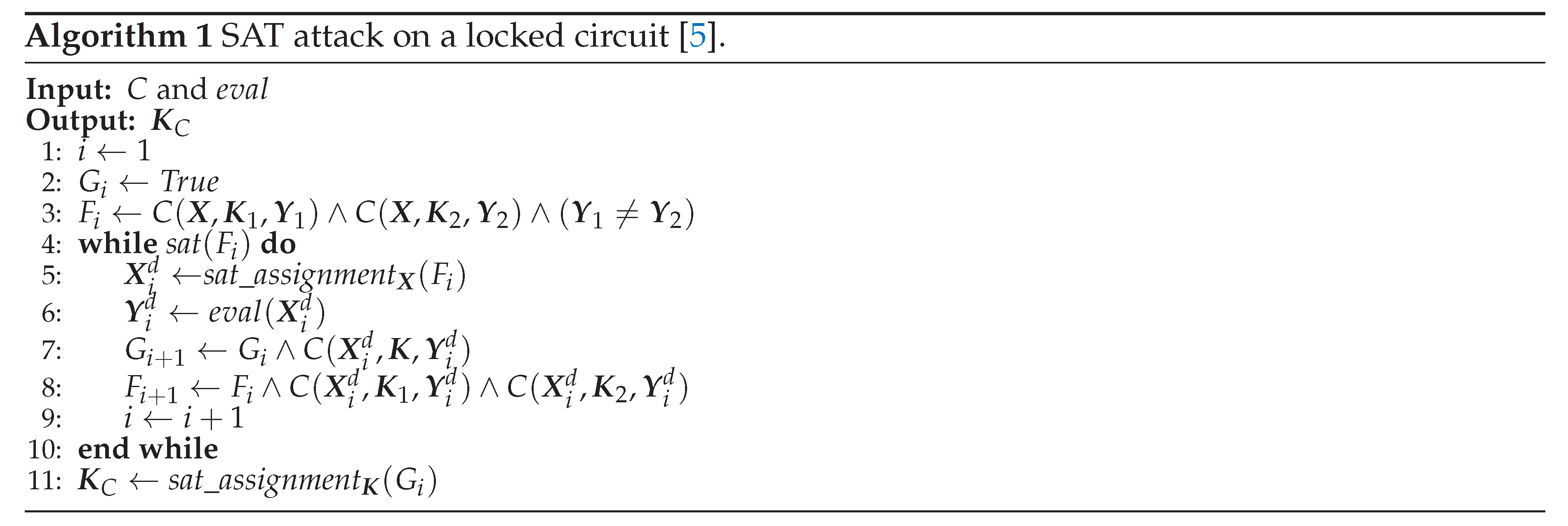
To determine the value of the key
, it is theoretically sufficient to use a SAT solver to find the key assignment
such that the formula is satisfiable. The problem is the possible existence of false keys, for which the given formula is also satisfiable. The authors in [
5] therefore proposed an algorithm, shown in Algorithm 1, that tries to eliminate false keys in two steps. In the first step, there is a search for so-called distinctive input pattern
, that for two different keys
and
outputs two different output patterns
and
.
is then the distinctive input pattern if
In the second step, the activated circuit is used with the distinctive input pattern to obtain the distinctive output pattern . Based on this observation, we can exclude one or both keys and from the class of possible correct keys. The database of distinctive patterns is iteratively built and the SAT solver finally determines the resulting secret key using it.
Algorithm 1 uses two subroutines, and . The routine returns True or False depending on whether is a satisfiable or unsatisfiable Boolean formula. The routine returns an assignment of logical values for the vector such that the Boolean formula is satisfiable.

4. Results
We tested the described attack from [
5], described in
Section 3 on 11 combinatorial circuits from the ISACS ’85 class. Basic information about these circuits can be seen in the
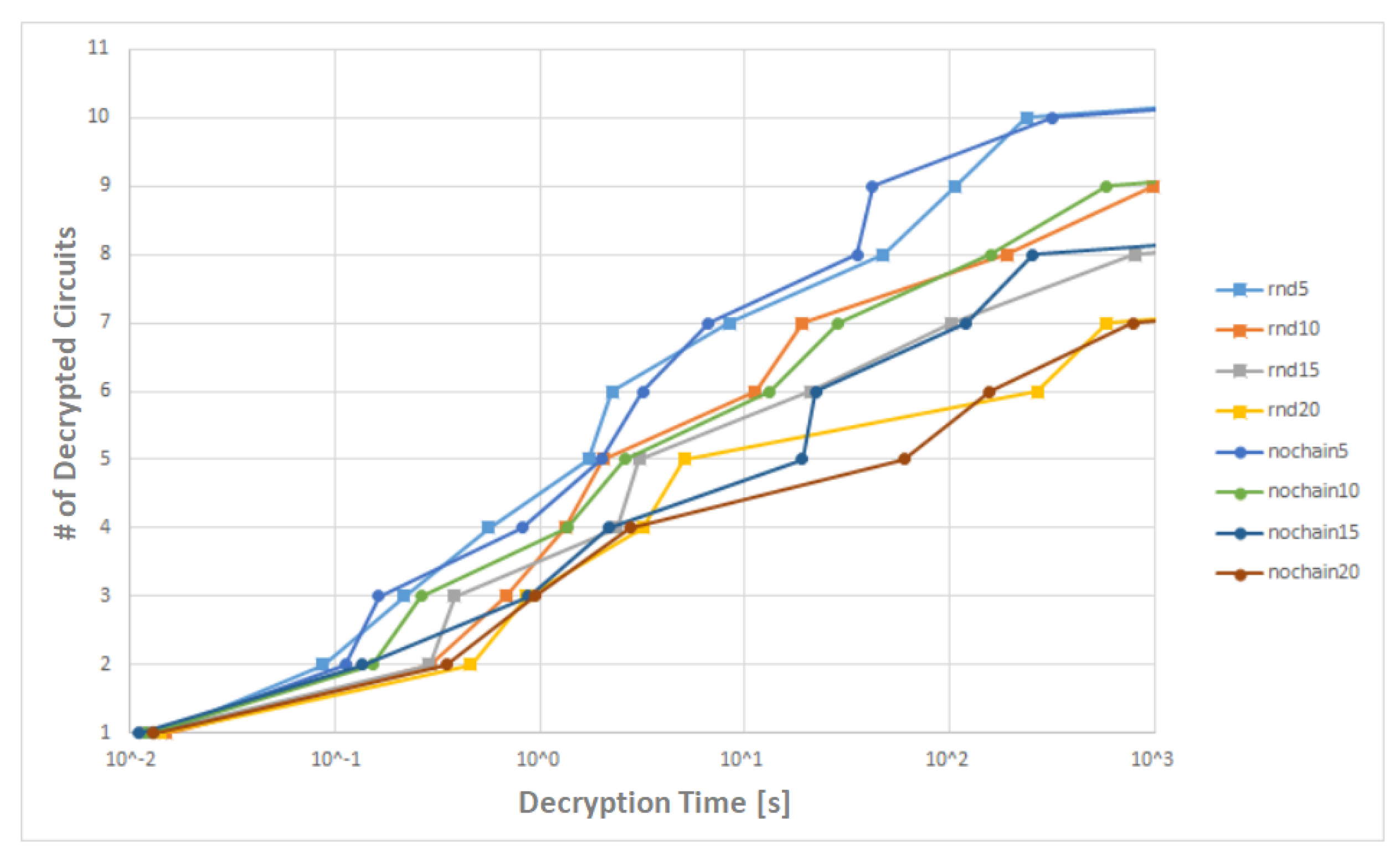
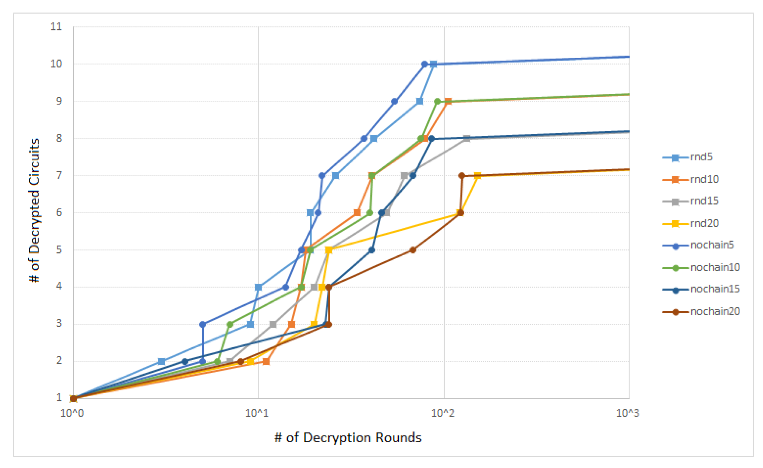
Table 2). We inserted key gates that represent 5%, 10%, 15%, and 20% of the total number of gates using two approaches: insertion into random wires (rnd lines in the
Figure 6 and
Figure 7) and insertion into random wires with chaining elimination (nochain lines in the
Figure 6 and
Figure 7). The exact number of inserted key bits is stated in the
Table 2 in the four right-most columns.
The locked circuits were subsequently attacked using the attack in the Algorithm 1. The CaDiCaL SAT solver [
21] was used for solving the SAT problem in the Algorithm 1. The choice for the CaDiCaL SAT solver was motivated by the fact that CaDiCaL was the winner of the SAT solver competition in the time of the research. Several other SAT solvers can be found on the international SAT competition webpage [
22]. Experiments were performed on an Intel Core i5-5200U CPU with 8GB RAM. The maximal attack running time was set to 1000 seconds.
We unlocked 10 of the 11 locked circuits with 5% of the key gates as can be seen on blue lines rnd5 and nochain5 in the
Figure 6. To use 5% of the key gates can be considered the most realistic scenario. One should realize that it is desired to add a minimum number of gates due to speed, power consumption and cost of the circuit as well.
The dependency of the number of unlocked circuits on the number of the decryption rounds (rounds necessary for unlocking), in other words also on the number of input-output pairs
is shown in the
Figure 7. As one can see, 100 pairs were enough to unlock 10 of the 11 locked circuits with 5% of the key gates.
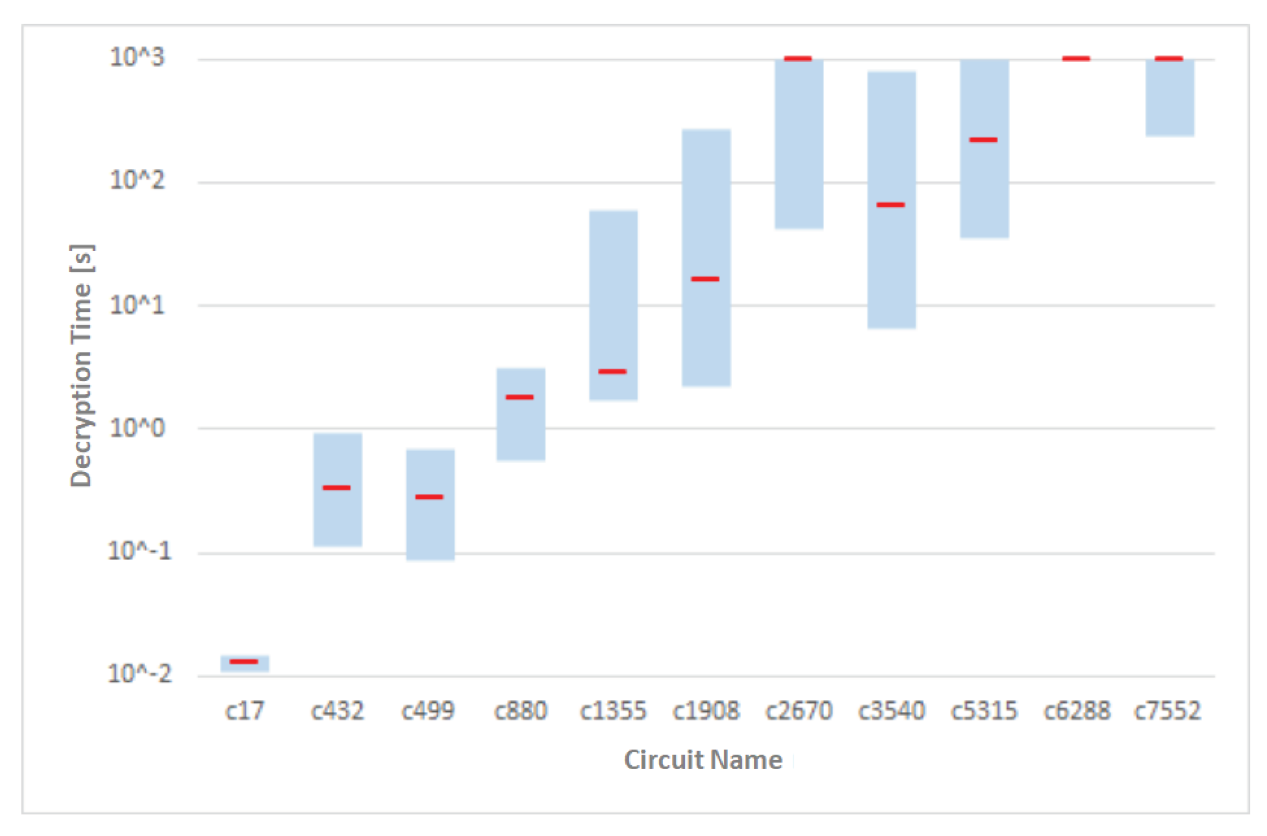
Figure 8 shows the graph of the distribution of the time required to unlock the 11 circuits that were locked using various approaches. The circuits are ordered in the graph according to the total number of gates in the ascending manner. The red mark denotes the median for the given circuit. We assumed that the higher number of gates will be result in the greater attack complexity. However, attacking the circuit
was more difficult than the next two bigger circuits. The circuit
however has more primary inputs and outputs.
It is also very interesting to take a bit closer look on the number of key bits (key gates). If we insert
n key bits into the circuit, it would take
time to try all possible keys, i.e. to use the so-called brute force attack. However, brute force attack is computationally infeasible for enough large values of
n. Nowadays secure value is
. As one can see in the
Figure 8, we were able to unlock all the circuits from the
with keys of lengths from 83 to 334 bits (see
Table 2).
5. Conclusions
To break the logic locking based on the insertion of key bits using XOR/XNOR gates there was an SAT solver-based attack proposed in [
5]. The aim of this work was to experimentally verify this attack on several locked circuits with various numbers of primary inputs and outputs and with various numbers of gates. Except for the random placement of the key gates, we evaluate also the positioning with chaining elimination. The obtained and presented results show that we were able to unlock 10 of 11 circuits within a few minutes on a common PC. It follows from the experiments that a higher number of primary inputs and outputs results in more input-output observations needed to unlock the circuit thus resulting in an attack time increase. The results presented in
Section 4 show the power of SAT solvers where it was possible to find keys of lengths exceeding the limits suggested nowadays. On the other hand, SAT solvers are struggling with limits concerning the number of clauses for the Boolean formula to be solved as well as the number of used Boolean variables. Thus only logical circuits of limited complexity can be attacked.
An interesting idea for future research is to use the so-called multiple right-hand sides (MRHS) equations, proposed in [
17], for attacks on logic locking. MRHS equations were also used in the cryptanalysis of block ciphers [
18]. This research way supports also the existence of the MRHS solver [
19].
Author Contributions
Conceptualization, F.J. and M.V.; methodology, F.J. and M.V.; software, F.J., J.K., and M.J. ; validation, J.K. and M.J.; formal analysis, F.J. and J.K.; writing—original draft preparation, F.J., J.K., M.V., and V.H.; writing—review and editing, V.H., M.V., and M.J.; visualization, F.J. and J.K.; supervision, M.V. and V.H.; funding acquisition, V.H., M.V., and M.J. All authors have read and agreed to the published version of the manuscript.
Funding
This project was funded by VEGA grant No. 1/0105/23 and by NATO Science for Peace and Security Programme under Grant G5985.
Acknowledgments
We would like to thank the anonymous reviewers for their comments and suggestions that improved this paper’s readability and content.
Conflicts of Interest
The authors declare no conflicts of interest.
Abbreviations
The following abbreviations are used in this manuscript:
| IoT |
Internet of Things |
| IC |
Integrated Circuit |
| ID |
Unique Identifier |
| FSM |
Finite State Machine |
| CPU |
Central Processor Unit |
| RAM |
Random Access Memory |
| GB |
Giga Byte |
| SAT |
Satisfiability |
References
- Suh, G.E.; Devadas, S. Physical Unclonable Functions for Device Authentication and Secret Key Generation. In Proceedings of the 44th ACM/IEEE Design Automation Conference, San Diego, CA, USA, 04–08 June 2007; pp. 9–14. [Google Scholar] [CrossRef]
- Koushanfar, F.; Qu, G.; Potkonjak, M. Intellectual Property Metering. IH 2001, LNCS 2001, 2137, 81–95. [Google Scholar] [CrossRef]
- Roy, J.A.; Koushanfar, F.; Markov, I.L. EPIC: Ending Piracy of Integrated Circuits. In Proceedings of the 2008 Design, Automation and Test in Europe, Munich, Germany, 10–14 March 2008; pp. 1069–1074. [Google Scholar] [CrossRef]
- Rajendran, J.; Pino, Y.; Sinanoglu, O.; Karri, R. Security Analysis of Logic Obfuscation. In Proceedings of the DAC Design Automation Conference 2012, San Francisco, CA, USA, 03–07 June 2012; pp. 83–89. [Google Scholar] [CrossRef]
- Subramanyan, P.; Ray, S.; Malik, S. Evaluating the security of logic encryption algorithms. In Proceedings of the 2015 IEEE International Symposium on Hardware Oriented Security and Trust (HOST), Washington, DC, USA, 05–07 May 2015; pp. 137–143. [Google Scholar] [CrossRef]
- Koushanfar, F.; Gang, Q. Hardware metering. In Proceedings of the 38th annual design automation conference 2001. pp. 490–493. [CrossRef]
- Kajtez, N.; Zhang, Y.; Halak, B. Lockit: A Logic Locking Automation Software. Electronics 2021, 10, 2817. [Google Scholar] [CrossRef]
- Mirmohammadi, Z.; Borujeni, S.E. A New Optimal Method for the Secure Design of Combinational Circuits against Hardware Trojans Using Interference Logic Locking. Electronics 2023, 12, 1107. [Google Scholar] [CrossRef]
- Nguyen, Q.-L.; Dupuis, S.; Flottes, M.-L.; Rouzeyre, B. SKG-Lock+: A Provably Secure Logic Locking SchemeCreating Significant Output Corruption. Electronics 2022, 11, 3906. [Google Scholar] [CrossRef]
- Baumgarten, A.; Tyagi, A.; Zambreno, J. Preventing IC Piracy Using Reconfigurable Logic Barriers. IEEE Design & Test of Computers 2010, 27, 66–75. [Google Scholar] [CrossRef]
- Divyanshu, D.; Kumar, R.; Khan, D.; Amara, S.; Massoud, Y. An Approach towards Designing Logic Locking Using Shape-Perpendicular Magnetic Anisotropy-Double Layer MTJ. Electronics 2023, 12, 479. [Google Scholar] [CrossRef]
- Divyanshu, D.; Kumar, R.; Khan, D.; Amara, S.; Massoud, Y. Design of VGSOT-MTJ-Based Logic Locking for High-Speed Digital Circuits. Electronics 2022, 11, 3537. [Google Scholar] [CrossRef]
- Alasad, Q.; Yuan, J.-S.; Bi, Y. Logic Locking Using Hybrid CMOS and Emerging SiNW FETs. Electronics 2017, 6, 69. [Google Scholar] [CrossRef]
- Yasin, M.; Rajendran, J.; Sinanoglu, O. A Brief History of Logic Locking. In Trustworthy Hardware Design: Combinational Logic Locking Techniques, Analog Circuits and Signal Processing; Springer International Publishing: Cham, Switzerland, 2020; pp. 17–31. [Google Scholar] [CrossRef]
- Zhou, J; Zhang, X. Generalized SAT-attack-resistant logic locking. IEEE Transactions on Information Forensics and Security 2021, 16, 2581–2592. [Google Scholar] [CrossRef]
- Zhou, J.; Zhang, X. A Low-Complexity Flexible Logic-Locking Scheme Resisting Removal Attacks. In IEEE International Midwest Symposium on Circuits and Systems (MWSCAS), Lansing, MI, USA, 09–11 August 2021, pp. 869–873. [CrossRef]
- Zajac, P. MRHS equation systems that can be solved in polynomial time. Tatra Mountains Mathematical Publications 2016, 67, 205–219. [Google Scholar] [CrossRef]
- Zajac, P. Algebraic Cryptanalysis with MRHS Equations Cryptography 2023, 7, 19. [CrossRef]
- Raddum, H.; Zajac, P. MRHS solver based on linear algebra and exhaustive search Journal of Mathematical Cryptology 2018, 12, pp. 143–157. [CrossRef]
- Zhong, Y.; Guin, U. Complexity Analysis of the SAT Attack on Logic Locking. IEEE Transactions on Computer-Aided Design of Integrated Circuits and Systems 2023, 42, pp–3143. [Google Scholar] [CrossRef]
- CaDiCaL. Simplified Satisfiability Solver. Available online: https://fmv.jku.at/cadical/ (accessed on March 3, 2024).
- The International SAT Competition Web Page. Available online: http://www.satcompetition.org/ (accessed on March 3, 2024).
|
Disclaimer/Publisher’s Note: The statements, opinions and data contained in all publications are solely those of the individual author(s) and contributor(s) and not of MDPI and/or the editor(s). MDPI and/or the editor(s) disclaim responsibility for any injury to people or property resulting from any ideas, methods, instructions or products referred to in the content. |
© 2024 by the authors. Licensee MDPI, Basel, Switzerland. This article is an open access article distributed under the terms and conditions of the Creative Commons Attribution (CC BY) license (http://creativecommons.org/licenses/by/4.0/).
