Submitted:
18 January 2024
Posted:
19 January 2024
You are already at the latest version
Abstract
We introduce a novel method for fabricating perovskite solar modules using selective spin-coating on various Au/ITO patterned substrates. These patterns were engineered for twofold purposes: (1) to enhance selectivity of monolayers primarily self-assembling on the Au electrode, and (2) to enable seamless interconnection between cells through direct contact of the top electrode and the hydrophobic Au connection electrode. Utilizing SAMs-treated Au/ITO, we achieved sequential selective deposition of the electron transport layer (ETL) and the perovskite layer on the hydrophilic amino-terminated ITO, while the hole transport layer (HTL) was deposited on the hydrophobic CH3-terminated Au connection electrodes. Importantly, our approach had negligible impact on the series resistance of the solar cells, as evidenced by the measured specific contact resistivity of the multilayers. A significant outcome was the production of a 6-cell series-connected solar module with a notable average PCE of 8.32%, providing a viable alternative to the conventional laser scribing technique.
Keywords:
Perovskite mini-module
; Self-assembled Monolayers
; Selective deposition
; Dewetting
; Connection Electrode
; Hexadecanethiol
1. Introduction
Hybrid organic-inorganic perovskites are of great interest owing to their outstanding optoelectronic properties [1,2,3,4,5], and easy and low-cost manufacturing processes [6,7]. These advantages pave the way for cost-effective and highly efficient solar cells. Consequently, efforts are underway to upscale perovskite solar cells into larger solar modules for market deployment [8,9,10,11,12]. Such modules can be constructed by dividing individual cells and integrating them via interconnections.
Traditionally, laser scribing has been preferred for creating thin-film solar modules [13,14,15,16,17,18,19]. This technique offers layer by layer precision in material removal using different laser wavelengths, facilitating detailed patterning of the modules with impressive resolution, processing speed, and selectivity. However, it's not flawless [20]. Laser damage [21,22], poor selectivity for the underlying layer, and metal particle contamination can lead to shunting [23,24,25,26]. Another shortcoming is the reliance on expensive equipment.
Selective patterning of solar cells can be an emerging alternative [27,28,29,30,31,32,33]. This method has the potential to address the challenges of laser processing. It offers a simplified, cost-effective means of producing modules with a high aperture ratio and is compatible with flexible manufacturing techniques.
A promising possibility in this field is the use of self-assembled monolayers (SAMs). SAMs are two-dimensional, ordered molecular arrangements on substrate surfaces. They possess the unique ability to modify surface properties based on their terminal groups. These groups determine the surface energy and functionality of the SAMs, making them either hydrophobic or hydrophilic [33,34,35,36,37]. This feature can be exploited for selective solvent wetting or de-wetting and can also affect the interaction of the solute with the surface [38]. By leveraging these traits, selective deposition of specific materials on predefined areas can be achieved, enabling precise solar module patterning.
In our study, we present a novel selective patterning process for fabricating perovskite solar minimodules. This process utilizes two different types of SAMs in combination with a spin-coating method. We designed an innovative heterogeneous (Au/ITO) patterned substrate, incorporating Au electrodes (called connection electrodes) on patterned ITO's edge. This design ensures selective deposition of the active layer on ITO regions and seamless interconnection between separated cells. Prior to depositing active layers like SnO2 and perovskite, we applied two distinct SAMs to the heterogeneous patterned surface, thereby increasing the deposition selectivity. We detail the underlying molecular mechanisms and interactions that facilitate this selective deposition.
Our experimental approach relies on SAMs like HDT (hexadecanethiol) and APTES (3-aminopropyl) triethoxysilane. These compounds demonstrate preferential attachment to the patterned surface due to specific molecular affinities. The resulting active layers, SnO2 NCs (ETL) and perovskite, are then selectively and sequentially deposited on this modified surface using a spin-coating technique. The evaluation techniques and results, culminating in the production of a minimodule are further discussed. Our approach not only addresses the limitations of the laser-scribing technique but also presents an efficient module fabrication technology.
2. Material and Methods
2.1. Materials
All the chemicals and materials were used as received, without further purification. Patterned ITO glass (10 Ω/sq) substrates were purchased from Freemteck (Seoul, South Korea). Lead iodide (PbI2, 99.999 % trace metal basis) was received from TCI (Tokyo, Japan). Methylammonium iodide (MAI, crystal) and 2,2',7,7'-Tetrakis[N,N-di(4-methoxyphenyl)amino]-9,9'-spirobifluorene (Spiro-OMeTAD, 99 %) were purchased from NCT Inc. (Seoul, South Korea). Tin (IV) oxide (SnO2, 15 % in H2O colloidal dispersion) was obtained from Alfa Aesar (Seoul, South Korea). The chemicals, including hexadecanethiol (HDT), 3-aminopropyltriethoxysilane (APTES, 99.999 %), methylamine hydrochloride (MACl, 98 %), Li-bis(trifluoromethanesulfonyl)imide (Li-salt, 99.95 %), dimethylsulfoxide (DMSO, 99.8 %), N,N-dimethylformamide (DMF, 99.8 %), chlorobenzene (anhydrous, 99.8 %), 4-tert-butyl pyridine (TBP, 98 %), acetonitrile (99.8 %), 2-propanol, acetone, and ethanol were purchased from Sigma-Aldrich (Seoul, South Korea).
2.2. Fabrication of Perovskite minimodule
Figure 1 shows a schematic pathway for the selective deposition of active layers on patterned ITO cells to make a perovskite minimodule.
The patterned ITO glass substrate is a starting substrate, which was fabricated by wet etching using photoresist (PR) mask produced by a conventional photolithography (Figure 1(a)). The patterned ITO was cleaned ultrasonically in acetone, isopropyl alcohol, and deionized (DI) water for 10 min each, and then dried with N2 gas. An E-beam evaporator under high vacuum (1x10⁻⁶ torr) was used to deposit the connection electrode consisting of Ti (100 nm) / Au (100 nm) through a shadow mask on the edge of each patterned ITO cell, making a heterogeneous (Au/ITO) structure (Figure 1(b)). The Au/ITO patterned substrate was then exposed to ultraviolet (UV)-ozone treatment for 30 min to activate ITO surface. The HDT monolayers were then selectively assembled on Au connection electrode of the cells by immersing the patterned glass in a solution of HDT (0.5 mM) in ethanol for 60 min at room temperature in an Ar-filled glove box, followed by rinsing with pure anhydrous ethanol and drying in N2 flow (Figure 1(c)). Next, the glass substrate was dipped in a solution of APTES (0.1 µl/ml) in pure anhydrous ethanol for 1 h at room temperature to attach APTES to an ITO surface (Figure 1(d)). The insets of Figure 1(c) and (d) show the structures of each SAMs. Subsequently, SnO2 NCs ETL and perovskite layers, dewetted from the hydrophobic connection electrodes, were selectively and sequentially spin-coated on previously prepared ITO, followed by the non-selective deposition of spiro-OMeTAD HTL on the substrate (Figure 1(e)). The conditions of the ETL and perovskite layer deposition were described in the previous work [38]. Finally, the top Au electrode (100 nm thick) was deposited by thermal evaporation under high vacuum (1x10⁻⁶ torr) through a shadow mask to electrically connect the isolated cells, thus creating perovskite-based mini-modules (Figure 1(f)). The inset of Figure 1(f) shows a multilayered contact structure formed on connection electrode for the integrated connection between cells.
2.3. Characterizations
The contact angles were measured using a Surface Electro Optics, SEO (Model: Phoenix 300) instrument at room temperature and relative humidity of 30-35%. The DI water (18 MΩ.cm) and other solutions were dropped onto the sample surface using a syringe needle and the droplet image was immediately recorded. The surface morphology was characterized by field-emission scanning electron microscopy (FESEM, JEOL-7610F, Japan). The X-ray photoelectron microscopy (XPS) data were analyzed utilizing a commercial system (K-alpha, Thermo VG, U.K.) equipped with a focused monochromatic Al Kα source (h: 1486.6 eV) and the beam spot size of 400 µm in diameter. The survey scans were controlled using a passing energy of 200 eV with a step size of 1 eV under ultrahigh vacuum of 3.6 x 10⁻⁹ torr. The contact resistance of transmission line method (TLM) patterns was measured by a Semiconductor parameter analyzer (HP4155C). The sheet resistances were measured using a four-point probe (CMT-series Changmin, Co. Ltd, Korea). The performance of perovskite solar cell and mini-module was evaluated by a solar simulator (Newport Oriel Solar Simulator) under AM 1.5G (100 mAcm-2) illumination. A standard Si solar cell (Oriel, VLSI Standard) was employed to calibrate the intensity of illuminated light.
3. Results and discussion
3.1. XPS Analysis of SAMs Assembled on UV-Exposed Substrates
We utilized two specific SAMs: the hydrophobic HDT-Au and the hydrophilic, reactive APTES-ITO. Prior to the SAM assembly process, we activated the ITO surface using UV-ozone treatment, enhancing APTES assembly. However, this treatment led to oxidation of the Au surface. To assess the UV exposure effects on Au and its influence on HDT assembly and hydrophobicity, we conducted XPS analysis.
Figure 2(a) presents the XPS spectrum of the UV-exposed Au (upper curve) and one post-ethanol dip at 25°C for 20 minutes (lower curve). The O 1s data from the upper spectrum features two peaks at 531 and 532.6 eV, indicating hydroxide Au(OH)₃ and either adsorbed water or an oxyhydroxide AuOOH (Au₂O₃H₂O), respectively [39,40]. These curves fit well with minor differences in binding energies and peak gaps, suggesting an oxidic adlayer primarily of AuOOH and some Au(OH)₃ after UV/ozone exposure. Conversely, the O 1s data from the ethanol-treated UV-exposed Au (lower spectrum) reveal a significant decrease in the AuOOH spectrum intensity, while the Au(OH)₃ intensity remains similar. This implies that ethanol treatment effectively reduces amount of oxyhydroxide by retaining a slight mixture of AuOOH and Au(OH)₃ on the gold surface.
Additionally, after exposing the Au to UV, it was immersed in the HDT solution to produce an HDT-assembled Au surface. We then used XPS to determine the influence of oxide layer on HDT assembly.
Figure 2(b) displays the S 2p XPS spectra of HDT SAMs on UV/ozone-treated gold. It comprises two doublets: a lower-intensity doublet at 164.2 eV (S 2p3/2) and 165.7 eV (S 2p1/2), indicating unbound sulfur atoms in HDT molecules, and a stronger doublet at 162 eV (S 2p3/2) and 163.2 eV (S 2p1/2), denoting chemically-bound sulfur on the gold surface [41,42,43,44,45]. These observations indicate that HDT monolayers self-assemble on UV/ozone-treated gold surfaces as a result of chemical interactions between sulfur and gold, despite the presence of gold oxide layer. Possible reasons include ethanol rinsing reducing the AuOOH layer thickness and thiol molecules in the solution oxidizing on the Au(OH)₃ and AuOOH surfaces, thus forming Au-S bonds via hydration [40].
In the previous paper, we discussed the self-assembly of APTES monolayer on ITO and its influence on subsequent SnO2 NCs ETL and perovskite active layer deposition. This monolayer on ITO covalently bonds with SnO2 NCs during spin-coating, leading to a uniform, pinhole-free SnO2 NC layer and promoting consistent growth of the perovskite film [38].
3.2. Contact Angle Measurements of the Precursors on SAMs-Treated Substrates
The phenomena of wetting and dewetting can be characterized by the contact angles of liquids forming on surfaces [46]. Typically, a contact angle ranging from 0° to 90° results in wetting, while angles exceeding 90° promote dewetting. Thus, the 90° mark serves as a general indicator of the transition from wetting to dewetting [47,48]. Additionally, the contact angle is affected by the solid substrate's chemical composition and surface roughness, as well as the liquid's chemical nature [49,50,51,52]. Taking it into account, we assessed the contact angle for all solutions used in our process on both HDT-assembled Au and APTES-assembled ITO.
Figure 3 illustrates the water contact angles and the angles of precursor solutions, including the SnO2 precursor, perovskite precursor, and spiro-OMeTAD precursor, on both HDT-treated gold and APTES-assembled ITO. A water contact angle of 82° was recorded for bare Au. This angle rose to 116° on HDT-assembled bare Au and further increased to 132° on HDT-assembled UV-treated Au. Such a rise suggests that the HDT monolayer on the gold oxide, when retained on the Au surface, significantly enhances its water repellency compared to HDT on bare Au.
To understand the dewetting properties of our process's precursors, we measured the contact angles for the SnO2 NC precursor, perovskite solution, and spiro-OMeTAD on HDT-assembled UV-exposed Au. The SnO2 NC and perovskite solutions exhibited contact angles of 114° and 92°, respectively. These values imply dewetting of the solutions on HDT-assembled Au, facilitating selective active layer patterning. On the other hand, the spiro-OMeTAD precursor had a notably low contact angle of 10°, indicating its wetting nature on the HDT surface. Finally, water's contact angle on APTES-assembled ITO was 52°, signaling a hydrophilic character promoting deposition of uniform SnO2 layer through covalent bonding [38].
3.3. Specific Resistance Measurement of Multi-layered Contact Structures
Given that spiro-OMeTAD was applied over the HDT-coated connection Au electrodes, it was essential to assess the impact of these patterning processes. We employed the TLM method [53] to evaluate three distinct structures: bare Au/Au; UV-treated Au/HDT SAMs/Au; and UV-treated Au/HDT SAMs/Spiro-OMeTAD/Au. Consequently, we derived four key parameters: specific contact resistivity (ρC), contact resistance (RC), sheet resistance (RSH), and transfer length (LT), using equation 1.
Figure 4 illustrates (a) TLM resistance measurements plotted against contact distance for three distinct configurations including bare Au/Au, UV-treated Au/HDT SAMs/Au, UV-treated Au/HDT SAMs/Spiro-OMeTAD/Au and (b) a schematic of the TLM pattern, where L = 1000 µm, W = 500 µm, and d represents contact distance.
The total resistance (RT) between two contacts (having length l and width W) separated by distance d in TLM patterns can be described by [11]:
Here, RC stands for contact resistance, and RSH is the sheet resistance of the underlying Au.
From Equation 1, the sheet resistance of the Au substrate can be deduced from the TLM plot's slope (equal to RSH/W). For the Au/HDT/Spiro-OMeTAD/Au configuration, it is approximately 0.51 ohm/square.
The transfer length, LT, is defined as the distance from a contact's edge where the current density value decreases to 1/e of its initial value. This can be expressed as [53,54]:
where RSK is the sheet resistance of the Au substrate directly beneath the contact. Assuming no alloying or sintering at the metal-SAMs layer interface, we consider RSK equal to the RSH of the Au substrate. Thus, LT is calculated as 98 µm (0.10 Ω × 500 µm / 0.51 Ω/□).
Therefore, the specific contact resistivity (ρC) can be deduced:
For Au-Au contact resistance, the result is negligible. In contrast, RC values for Au/HDT SAMs/Au and Au/HDT SAMs/Spiro-OMeTAD/Au are approximately 0.02 Ω and 0.10 Ω, respectively.
The SAMs' contribution to specific contact resistivity is 2.17 ×10⁻⁶ Ω-cm2 (calculated as 0.02 Ω × 500 µm × 21.7 µm). Similarly, for Au/HDT SAMs/Spiro-OMeTAD/Au, it's 4.9 × 10⁻⁵ Ω-cm2 (0.10 Ω × 500 µm × 98 µm). Table1 shows the extracted parameters for each contact structure.
3.4. Resolution in Selective Patterning from Au/ITO Line-Space Patterns
Figure 5 illustrates the sequential spin-coating of active layers, namely SnO2 NCs and perovskite, on mixed Au/ITO line-space patterns: (a) A schematic of the heterogeneous Au/ITO line-space patterns and optical images showing 9 Au lines; (b) SEM images capturing the selective deposition of active layers on the Au/ITO patterns, varying line widths from 50 µm to 1000 µm; (c) Close-up SEM images demonstrate the selective perovskite deposition on ITO: It’s evident that a 200 µm-wide Au line lacks deposition, although some coatings are present on the edges.
Sequential selective deposition's pattern resolution was exhibited by successively spin-coating the SnO2 NCs and perovskite solutions onto the specialized Au/ITO patterns. Interestingly, lines with width ranging from 1000 µm to 100 µm exhibited superior selective patterning but narrowing the width to 50 µm probably resulted in a loss of the selectivity. It is worth noting that the right inset (bottom) in Figure 5(c) shows an undulating Au-perovskite interface near a 200 µm-wide Au line’s edge, spanning approximately 15 µm. This irregularity may result from the imperfect pinning of the hydrophilic solution on boundaries. For instance, a hydrophilic-hydrophobic interface could cause liquid to accumulate briefly before breaking free, resulting in a wavy interface. While several factors could influence this wavy growth, further investigations are required to comprehend and optimize the process.
Besides the intrusion of perovskite into the hydrophobic Au line, insets also draw attention to an Au surface devoid of perovskite, alongside the superior microstructure of the perovskite itself. The encroachment width of perovskite into the Au line fluctuates between 4-15 µm for Au lines with widths spanning 100 µm to 1000 µm. Consequently, Au lines of width equal to 50 µm likely lack selectivity due to perovskite's lateral expansion from edge sites. These observations lead to conclusion that reliable selective patterning is feasible up to an Au line width of 100 µm.
Regarding module efficiency, the "dead area" or Wd noted in this research measures approximately 1900 µm. Given the cell segment width (Wa + Wd) of 7 mm, the active area fraction is 0.73. Impressively, this represents the very first successful perovskite module patterned through the consecutive spin-coating of active layers, with a commendable aperture ratio. Notably, employing a 200 µm connection electrode can dramatically increase the active area ratio to 0.84, a figure comparable with laser scribing methods. Moreover, due to innovative wet etching and shadow mask technologies, where the pattern resolution may be approximately 50 µm, the active area ratio can be effortlessly elevated to 0.96.
3.5. Electrical Performance of Perovskite Single Cells and Mini-Modules
We employed selective patterning techniques to produce six-segment series-connected perovskite solar modules. A single solar cell, measuring 0.09 cm2, was also fabricated using this selective process to serve as a performance benchmark for the larger modules.
An inset highlights a sample containing four individual cells, created through the selective method. Here, active layers were spin-coated on the APTES-coated active region of ITO and repelled from the HDT-coated Au electrodes situated on both the bottom and top ITO electrodes.
Figure 6(a) displays the J-V curve of a single solar cell, which has an average Power Conversion Efficiency (PCE) of 13.28%. It achieved a Jsc of 22.2 mA/cm2, a Voc of 1.02 V, and a Fill Factor (FF) of 0.68 under forward bias (as summarized in Table 1). Analyzing the J-V curve, we extracted Rsh values near zero bias and an Rs value at a Voc bias from the inverse of the J-V slope, respectively. These values are 500 Ω and 5.98 Ω, respectively. Such data suggest that our SAM-facilitated single cell exhibits superior selectivity over the HDT-coated Au electrode, combined with a high-performing solar cell that has notably low contact resistance and elevated shunt resistance.
In Figure 6(b), the I-V curve represents a solar module with six interconnected cells. This module yielded an average PCE of 8.32%, Voc of 5.39 V, FF of 0.56, and a Jsc of 2.76 mA/cm2. Additionally, its Rsh and Rs values are 600 Ω and 12.31 Ω, respectively. When compared with the single cell's metrics, similar outcomes emerge: similar FF, shunt resistance, and selectivity. However, the series resistance is marginally increased. Furthermore, the achieved Voc (5.39 V) is slightly below the anticipated 6.0 V, which can be attributed to the uneven active layer coatings.
In summary, the module's performance showcased a Voc of 5.39 V, Jsc of 2.76 A/cm2, and FF of 0.56. This culminates in a PCE of 8.32% over an active area measuring 2.14 cm2. Although minor variations exist, the photovoltage remains closely aligned with that of individual cells. This consistency underscores the efficacy of our innovative spin process and the specialized connection electrode system, signifying our successful scale-up to larger modules.
Conclusions
In this paper, we introduced an innovatory selective deposition-based patterning method for the fabricating of perovskite solar modules, effectively bypassing the need for traditional laser scribing techniques. Leveraging the unique characteristics of Au/ITO patterned cells, our approach utilized hydrophobic HDT-assembled Au as connection electrodes and hydrophilic APTES-functionalized ITO to optimize layer interactions during sequential spin dewetting.
Key findings and implications include:
Enhanced Selectivity: Our methodology ensured selective deposition of active layers on Au/ITO patterns, achieving a patterning resolution of approximately 100 µm. This can be further optimized in future iterations.
Efficient Interface Interaction: UV exposure played a key role in improving the quality of the APTES monolayer on ITO, effectively promoting the interaction with SnO2 NCs ETL, simultaneously forming a gold oxide layer on Au. This approach, confirmed by XPS, marked the hydrophobic properties of the assembled structure.
Low Specific Contact Resistivity: The integration of interconnection between the isolated cells was accomplished by direct contact of top electrode on the HTL with coated on HDT-Au connection electrode. As a result, the multilayered-contact structure consisting of Au/HDT/HTL/Au was obtained and its specific contact resistivity measured by TLM method was 4.9 x 10⁻⁵ Ω-cm2.
Promising Performance Metrics: The 6-subcell series-connected solar modules, produced using our method, showed an average PCE of 8.32%, Voc of 5.39 V, FF of 0.56, and Jsc of 2.76 mA/cm2.
This research emphasizes the potential of selective spin-coating-based patterning as a viable and scalable solution for large-scale perovskite solar module fabrication. Future work may focus on further optimization of this technique and its possible applications in the solar industry.
Author Contributions
Conceptualization, Son Singh; Methodology, Son Singh, Rahim Abdur and Md Abdul Kuddus Sheikh; Software, Ho-Seok Nam; Validation, Rahim Abdur, Bhabani Sankar Swain, Jindong Song and Jae-Hun Kim; Formal Analysis, Son Singh, Rahim Abdur, Md Abdul Kuddus Sheikh and Ho-Seok Nam; Investigation, Son Singh; Resources, Jaegab Lee; Data Curation, Son Singh; Writing-Original Draft Preparation, Son Singh; Writing-Review & Editing, Jaegab Lee; Visualization, Bhabani Sankar Swain, Jindong Song, Jea-Hun Kim, Sung Hyon Kim and Hyunseung Lee; Supervision, Jaegab Lee; Project Administration, Jaegab Lee; Funding Acquisition, Jaegab Lee.
Funding
This research work was supported by the National Research Foundation of Korea (NRF). funded by the Ministry of Science and ICT (Grant Number: 2022R1A5A7000765).
Data Availability Statements
The data presented in this study are available on request from the corresponding author.
Conflicts of Interest
The authors declare no conflict of interest.
References
- Min: H.; Lee, D. Y.; Kim, J.; Kim, G.; Lee, K. S.; Kim, J.; Paik, M. J.; Kim, Y. K.; Kim, K. S.; Kim, M. G.; Shin, T. J.; Il S., S. Perovskite Solar Cells with Atomically Coherent Interlayers on SnO2 Electrodes. Nature 2021, 598 (7881), 444–450. [CrossRef]
- Lin, Q.; Armin, A.; Nagiri, R. C. R.; Burn, P. L.; Meredith, P. Electro-Optics of Perovskite Solar Cells. Nat. Photonics 2015, 9 (2), 106–112. [CrossRef]
- Liu, Y.; Sun, J.; Yang, Z.; Yang, D.; Ren, X.; Xu, H.; Yang, Z.; Liu, S. F. 20-mm-Large Single-Crystalline Formamidinium-Perovskite Wafer for Mass Production of Integrated Photodetectors. Adv. Opt. Mater. 2016, 4 (11), 1829–1837. [CrossRef]
- Liu, Y.; Zhang, Y.; Zhao, K.; Yang, Z.; Feng, J.; Zhang, X.; Wang, K.; Meng, L.; Ye, H.; Liu, M.; Liu, S. (Frank). A 1300 mm2 Ultrahigh-Performance Digital Imaging Assembly Using High-Quality Perovskite Single Crystals. Adv. Mater. 2018, 30 (29), 1–11. [CrossRef]
- Shi, D.; Adinolfi, V.; Comin, R.; Yuan, M.; Alarousu, E.; Buin, A.; Chen, Y.; Hoogland, S.; Rothenberger, A.; Katsiev, K.; Losovyj, Y.; Zhang, X.; Dowben, P. A.; Mohammed, O. F.; Sargent, E. H.; Bakr, O. M. Shi D. et Al. Low Trap-State Density and Long Carrier Diffusion in Organolead Trihalide Perovskite Single Crystals //Science. – 2015. – V. 347. – №. 6221. – P. 519-522. 2015, 347 (6221), 519–522.
- Swain, B. S.; Singh, S.; Abdur, R.; Kim, J. H.; Lee, J. Combined Ultraviolet Ozone and Thermally Activated Formamidinium Iodide Solution to Fabricate Large Grain FAPbI2.6Br0.3Cl0.1 Films. ACS Omega 2023, 8 (10), 9298–9306. [CrossRef]
- Cai, M.; Wu, Y.; Chen, H.; Yang, X.; Qiang, Y.; Han, L. Cost-Performance Analysis of Perovskite Solar Modules. Adv. Sci. 2017, 4 (1). [CrossRef]
- Matteocci, F.; Razza, S.; Di Giacomo, F.; Casaluci, S.; Mincuzzi, G.; Brown, T. M.; D’Epifanio, A.; Licoccia, S.; Di Carlo, A. Solid-State Solar Modules Based on Mesoscopic Organometal Halide Perovskite: A Route towards the up-Scaling Process. Phys. Chem. Chem. Phys. 2014, 16 (9), 3918–3923. [CrossRef]
- Razza, S.; Di Giacomo, F.; Matteocci, F.; Cinà, L.; Palma, A. L.; Casaluci, S.; Cameron, P.; D’Epifanio, A.; Licoccia, S.; Reale, A.; Brown, T. M.; Di Carlo, A. Perovskite Solar Cells and Large Area Modules (100 cm2) Based on an Air Flow-Assisted PbI2 Blade Coating Deposition Process. J. Power Sources 2015, 277, 286–291. [CrossRef]
- Seo, J.; Park, S.; Kim, Y. C.; Jeon, N. J.; Noh, J. H.; Yoon, S. C.; Il S., S. Benefits of Very Thin PCBM and LiF Layer for Solution-Processed P-I-N Perovskite Solar Cells. Energy Environ. Sci. 2014, 7, 2642-2646. [CrossRef]
- Matteocci, F.; Cina, L.; Giacomo, F. D.; Razza, S.; Palma, A. L.; Guidobaldi, A.; D’Epifanio, A.; Licoccia, S.; Brown, T. M.; Reale, A.; Carlo, A. D. High efficiency photovoltaic module based on mesoscopic organometal halide perovskite. Prog. Photovoltaics Res. Appl. 2016, 24 (4), 436-445. [CrossRef]
- Agresti, A.; Pescetelli, S.; Palma, A. L.; Del Rio Castillo, A. E.; Konios, D.; Kakavelakis, G.; Razza, S.; Cinà, L.; Kymakis, E.; Bonaccorso, F.; Di Carlo, A. Graphene Interface Engineering for Perovskite Solar Modules: 12.6% Power Conversion Efficiency over 50 cm2 Active Area. ACS Energy Lett. 2017, 2 (1), 279–287. [CrossRef]
- Walter, A.; Moon, S. J.; Kamino, B. A.; Lofgren, L.; Sacchetto, D.; Matteocci, F.; Taheri, B.; Bailat, J.; Di Carlo, A.; Ballif, C.; Nicolay, S. Closing the Cell-to-Module Efficiency Gap: A Fully Laser Scribed Perovskite Minimodule with 16% Steady-State Aperture Area Efficiency. IEEE J. Photovoltaics 2018, 8 (1), 151–155. [CrossRef]
- Palma, A. L.; Matteocci, F.; Agresti, A.; Pescetelli, S.; Calabrò, E.; Vesce, L.; Christiansen, S.; Schmidt, M.; Di Carlo, A. Laser-Patterning Engineering for Perovskite Solar Modules with 95% Aperture Ratio. IEEE J. Photovoltaics 2017, 7 (6), 1674–1680. [CrossRef]
- Mincuzzi, G.; Palma, A. L.; DiCarlo, A.; Brown, T. M. Laser Processing in the Manufacture of Dye-Sensitized and Perovskite Solar Cell Technologies. ChemElectroChem 2016, 3 (1), 9–30. [CrossRef]
- Haas, S.; Gordijn, A.; Stiebig, H. High Speed Laser Processing For Monolithical Series Connection of Silicon Thin-film Modules. Prog. Photovoltaics Res. Appl. 2008, 16 (3), 195-203. [CrossRef]
- Chen, S.; Dai, X.; Xu, S.; Jiao, H.; Zhao, L.; Huang, J. Stabilizing Perovskite-Substrate Interfaces for High-Performance Perovskite Modules. Science 2021, 373 (6557), 902–907. [CrossRef]
- Han, G. S.; Kim, J.; Bae, S.; Han, S.; Kim, Y. J.; Gong, O. Y.; Lee, P.; Ko, M. J.; Jung, H. S. Spin-Coating Process for 10 cm × 10 cm Perovskite Solar Modules Enabled by Self-Assembly of SnO2 Nanocolloids. ACS Energy Lett. 2019, 4 (8), 1845–1851. [CrossRef]
- Moon, S. J.; Yum, J. H.; Lofgren, L.; Walter, A.; Sansonnens, L.; Benkhaira, M.; Nicolay, S.; Bailat, J.; Ballif, C. Laser-Scribing Patterning for the Production of Organometallic Halide Perovskite Solar Modules. IEEE J. Photovoltaics 2015, 5 (4), 1087–1092. [CrossRef]
- Galagan, Y. Stability of Perovskite PV Modules. JPhys Energy 2020, 2 (2), 0–6. [CrossRef]
- Bayer, L.; Ye, X.; Lorenz, P.; Zimmer, K. Studies on Perovskite Film Ablation and Scribing with Ns-, Ps- and Fs-Laser Pulses. Appl. Phys. A Mater. Sci. Process. 2017, 123 (10), 1–8. [CrossRef]
- Palma, A. L. Laser-Processed Perovskite Solar Cells and Modules. Sol. RRL 2020, 4 (4), 1–19. [CrossRef]
- Breitenstein, O.; Langenkamp, M.; Lang, O.; Schirrmacher, A. Shunts Due to Laser Scribing of Solar Cells Evaluated by Highly Sensitive Lock-in Thermography. Sol. Energy Mater. Sol. Cells 2001, 65 (1), 55–62. [CrossRef]
- Razza, S.; Pescetelli, S.; Agresti, A.; Di Carlo, A. Laser Processing Optimization for Large-Area Perovskite Solar Modules. Energies 2021, 14 (4). [CrossRef]
- Sinha, A.; Bliss, M.; Wu, X.; Roy, S.; Gottschalg, R.; Gupta, R. Cross-Characterization for Imaging Parasitic Resistive Losses in Thin-Film Photovoltaic Modules. J. Imaging 2016, 2 (3), 1–19. [CrossRef]
- Carolus, J.; Merckx, T.; Purohit, Z.; Tripathi, B.; Boyen, H. G.; Aernouts, T.; De Ceuninck, W.; Conings, B.; Daenen, M. Potential-Induced Degradation and Recovery of Perovskite Solar Cells. Sol. RRL 2019, 3 (10), 1–3. [CrossRef]
- Pasquali, M.; Carolan, P.; Sergeant, S.; Meersschaut, J.; Spampinato, V.; Conard, T.; Viva, A.; De Gendt, S.; Armini, S. Understanding Selectivity Loss Mechanisms in Selective Material Deposition by Area Deactivation on 10 nm Cu/SiO2 Patterns. ACS Appl. Electron. Mater. 2022, 4 (4), 1703–1714. [CrossRef]
- Zhang, Y.; Discekici, E. H.; Burns, R. L.; Somervell, M. H.; Hawker, C. J.; Bates, C. M. Single-Step, Spin-on Process for High Fidelity and Selective Deposition. ACS Appl. Polym. Mater. 2020, 2 (2), 481–486. [CrossRef]
- Zhang, Y.; D’Ambra, C. A.; Katsumata, R.; Burns, R. L.; Somervell, M. H.; Segalman, R. A.; Hawker, C. J.; Bates, C. M. Rapid and Selective Deposition of Patterned Thin Films on Heterogeneous Substrates via Spin Coating. ACS Appl. Mater. Interfaces 2019, 11 (23), 21177–21183. [CrossRef]
- Bao, Z. Fine Printing. Nat. Mater. 2004, 3 (3), 137–138. [CrossRef]
- Bhandaru, N.; Das, A.; Salunke, N.; Mukherjee, R. Ordered Alternating Binary Polymer Nanodroplet Array by Sequential Spin Dewetting. Nano Lett. 2014, 14 (12), 7009–7016. [CrossRef]
- Sehgal, A.; Ferreiro, V.; Douglas, J. F.; Amis, E. J.; Karim, A. Pattern-Directed Dewetting of Ultrathin Polymer Films. Langmuir 2002, 18 (18), 7041–7048. [CrossRef]
- Hashemi, F. S. M.; Prasittichai, C.; Bent, S. F. A New Resist for Area Selective Atomic and Molecular Layer Deposition on Metal-Dielectric Patterns. J. Phys. Chem. C 2014, 118 (20), 10957–10962. [CrossRef]
- Ulman, A. Formation and Structure of Self-Assembled Monolayers. Chem. Rev. 1996, 96 (4), 1533-1554. [CrossRef]
- Love, J. C.; Estroff, L. A.; Kriebel, J. K.; Nuzzo, R. G.; Whitesides, G. M. Self-Assembled Monolayers of Thiolates on Metals as a Form of Nanotechnology. Chem. Rev. 2005, 105 (4), 1103-1169. [CrossRef]
- Mackus, A. J. M.; Merkx, M. J. M.; Kessels, W. M. M. From the Bottom-Up: Toward Area-Selective Atomic Layer Deposition with High Selectivity †. Chem. Mater. 2019, 31 (1), 2–12. [CrossRef]
- Seo, E. K.; Lee, J. W.; Sung-Suh, H. M.; Sung, M. M. Atomic Layer Deposition of Titanium Oxide on Self-Assembled-Monolayer-Coated Gold. Chem. Mater. 2004, 16 (10), 1878–1883. [CrossRef]
- Singh, S.; Abdur, R.; Nam, H. S.; Kim, J. H.; Lee, S. M.; Lee, H.; Lee, J. Surface Functionalization of Indium Tin Oxide Electrodes by Self-Assembled Monolayers for Direct Assembly of Pre-Synthesized SnO2 Nanocrystals as Electron Transport Layers. Electron. Mater. Lett. 2023, 19 (3), 267–277. [CrossRef]
- Peuckert, M.; Coenen, F. P.; Bonzel, H. P. On the Surface Oxidation of a Gold Electrode in 1N H2S04 Electrolyte. Surf. Sci. 1984, 141 (2–3), 515–532. [CrossRef]
- King, D. E. Oxidation of Gold by Ultraviolet Light and Ozone at 25 °C. J. Vac. Sci. Technol. A Vacuum, Surfaces, Film. 1995, 13 (3), 1247–1253. [CrossRef]
- Park, T.; Kang, H.; Seong, S.; Han, S.; Son, Y. J.; Ito, E.; Hayashi, T.; Hara, M.; Noh, J. Formation and Structure of Highly Ordered Self-Assembled Monolayers by Adsorption of Acetyl-Protected Conjugated Thiols on Au(111) in Tetrabutylammonium Cyanide Solution. J. Phys. Chem. C 2019, 123 (14), 9096–9104. [CrossRef]
- Cristina, L. J.; Ruano, G.; Salvarezza, R.; Ferrón, J. Thermal Stability of Self-Assembled Monolayers of n-Hexanethiol on Au(111)-(1 × 1) and Au(001)-(1 × 1). J. Phys. Chem. C 2017, 121 (50), 27894–27904. [CrossRef]
- Calam, T. T.; Hasdemir, E. Comparative Characterizations of Self-Assembled Monolayers of 1,6-Hexanedithiol and 1-Hexanethiol Formed on Polycrystalline Gold Electrode. Comptes Rendus L’Academie Bulg. des Sci. 2019, 72 (3), 316–326. [CrossRef]
- Castner, D. G.; Hinds, K.; Grainger, D. W. X-Ray Photoelectron Spectroscopy Sulfur 2p Study of Organic Thiol and Bisulfide Binding Interactions with Gold Surfaces. Langmuir 1996, 12 (21), 5083–5086. https://doi.org/10.1021/la960465w.
- Allara, D. L.; Tao, Y.; Laibinis, P. E.; Parikh, A. N.; Nuzzo, R. G.; Uniuerstty, H.; Uniuersity, S.; Park, U.; Hill, M.; Jerser, N. Comparison of the Structures and Wetting Properties of Self-Assembled Monolayers of n-Alkanethiols on the Coinage Metal Surfaces, Cu , Ag , Aul. J. Am. Chem. Soc. 1991, 119 (13), 7152-7167. [CrossRef]
- Lipowsky, R.; Lenz, P.; Swain, P. S. Wetting and Dewetting of Structured and Imprinted Surfaces. Colloids Surfaces A Physicochem. Eng. Asp. 2000, 161 (1), 3–22. [CrossRef]
- Commentary, G. Definitions for Hydrophilicity, Hydrophobicity, and Superhydrophobicity: Getting the Basics Right. J. Phys. Chem. Lett. 2014, 5 (4), 686–688. [CrossRef]
- Samuel, B.; Zhao, H.; Law, K. Y. Study of Wetting and Adhesion Interactions between Water and Various Polymer and Superhydrophobic Surfaces. J. Phys. Chem. C 2011, 115 (30), 14852–14861. [CrossRef]
- Krainer, S.; Hirn, U. Contact Angle Measurement on Porous Substrates: Effect of Liquid Absorption and Drop Size. Colloids Surfaces A Physicochem. Eng. Asp. 2021, 619, 126503. [CrossRef]
- Law, K. Y. Contact Angle Hysteresis on Smooth/Flat and Rough Surfaces. Interpretation, Mechanism, and Origin. Accounts Mater. Res. 2022, 3 (1), 1–7. [CrossRef]
- Kvitek, L.; Saran, D.; Vaclavek, L.; Kapusta, J.; Kozmin, P. Influence of Surface Structures on Wettability. IOP Conf. Ser. Mater. Sci. Eng. 2021, 1178 (1), 012038. [CrossRef]
- Slepickova Kasalkova, N.; Slepicka, P.; Kolska, Z.; Svorcik, V. Wettability and Other Surface Properties of Modified Polymers. Wetting and Wettability 2015. [CrossRef]
- Reeves, G.H.; Harrison, H. B. Obtaining the Specific Contact Resistance from Transmission Line Model Measurements. IEEE Elect. Device Lett. 1982, 3 (5), 111–113. [CrossRef]
- Guo, S.; Gregory, G.; Gabor, A. M.; Schoenfeld, W. V.; Davis, K. O. Detailed Investigation of TLM Contact Resistance Measurements on Crystalline Silicon Solar Cells. Sol. Energy 2017, 151, 163–172. [CrossRef]
- Rakocevic, L.; Gehlhaar, R.; Merckx, T.; Qiu, W.; Paetzold, U. W.; Fledderus, H.; Poortmans, J. Interconnection Optimization for Highly Efficient Perovskite Modules. IEEE J. Photovoltaics 2017, 7 (1), 404–408. [CrossRef]
Figure 1.
shows the schematic pathway for the selective deposition of active layers on patterned ITO cells to make a perovskite mini-module: (a) a patterned ITO glass substrate; (b) a heterogeneous (Au/ITO) structure fabricated by evaporating a Ti/Au bilayer connection electrode on the edge of each patterned ITO cell through a shadow mask; (c) HDT monolayers selectively assembled on UV-exposed Au connection electrode and the structure of HDT monolayers; (d) APTES monolayers selectively assembled on ITO surface and the structure of APTES monolayers; (e) selective deposition of SnO2 NCs ETL and perovskite layer, followed by the non-selective deposition of spiro-OMeTAD HTL; (f) thermally evaporated top electrode through the shadow mask, which was in contact with the connection electrode, leading to the multilayered contact structure, as shown in the inset of Figure 1(f).
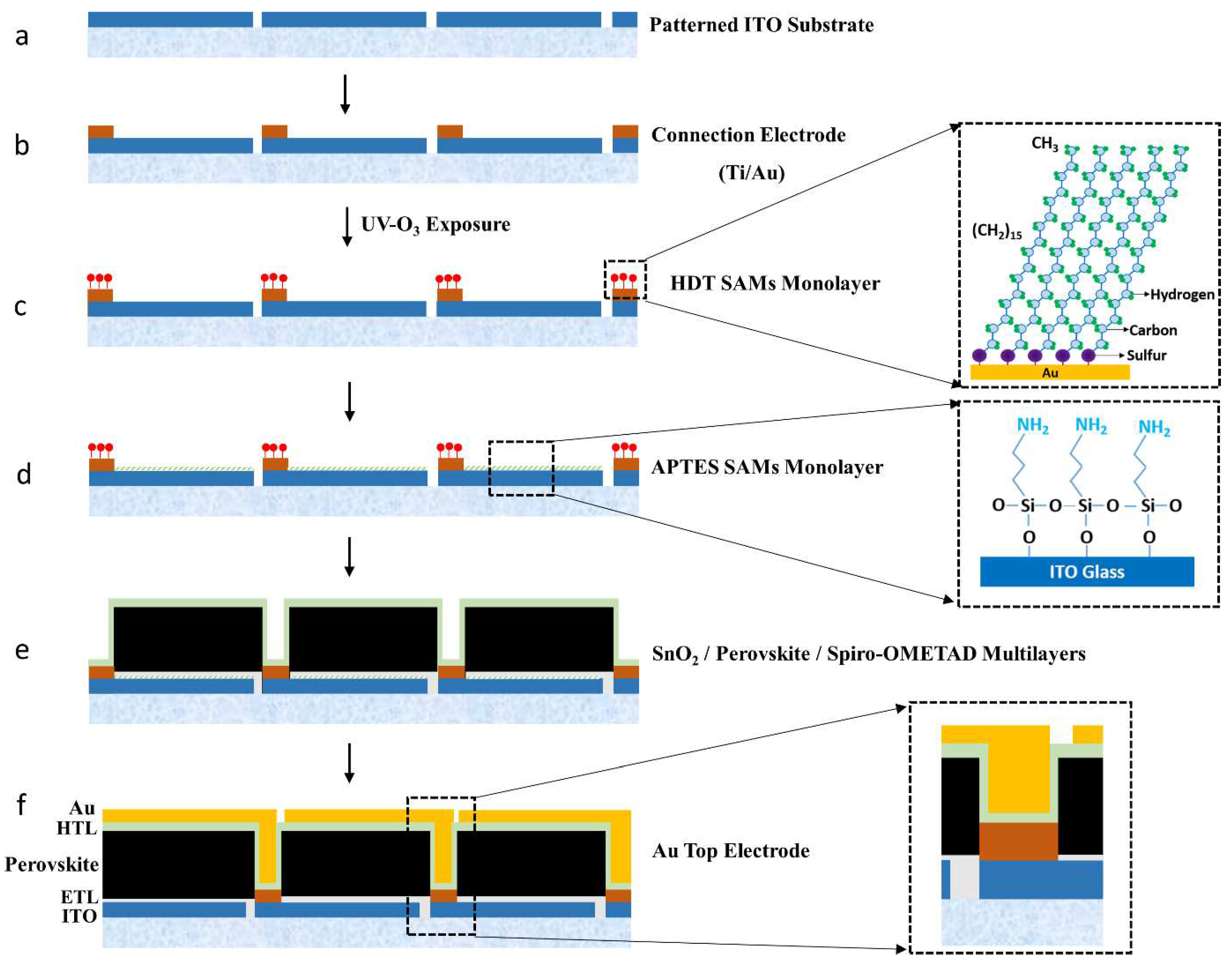
Figure 2.
shows (a) the XPS spectrum of the UV-exposed Au (upper curve) and one post-ethanol dip at 25°C for 20 minutes (lower curve) and (b) the S 2p XPS spectra of HDT SAMs on UV/ozone-treated gold.
Figure 2.
shows (a) the XPS spectrum of the UV-exposed Au (upper curve) and one post-ethanol dip at 25°C for 20 minutes (lower curve) and (b) the S 2p XPS spectra of HDT SAMs on UV/ozone-treated gold.
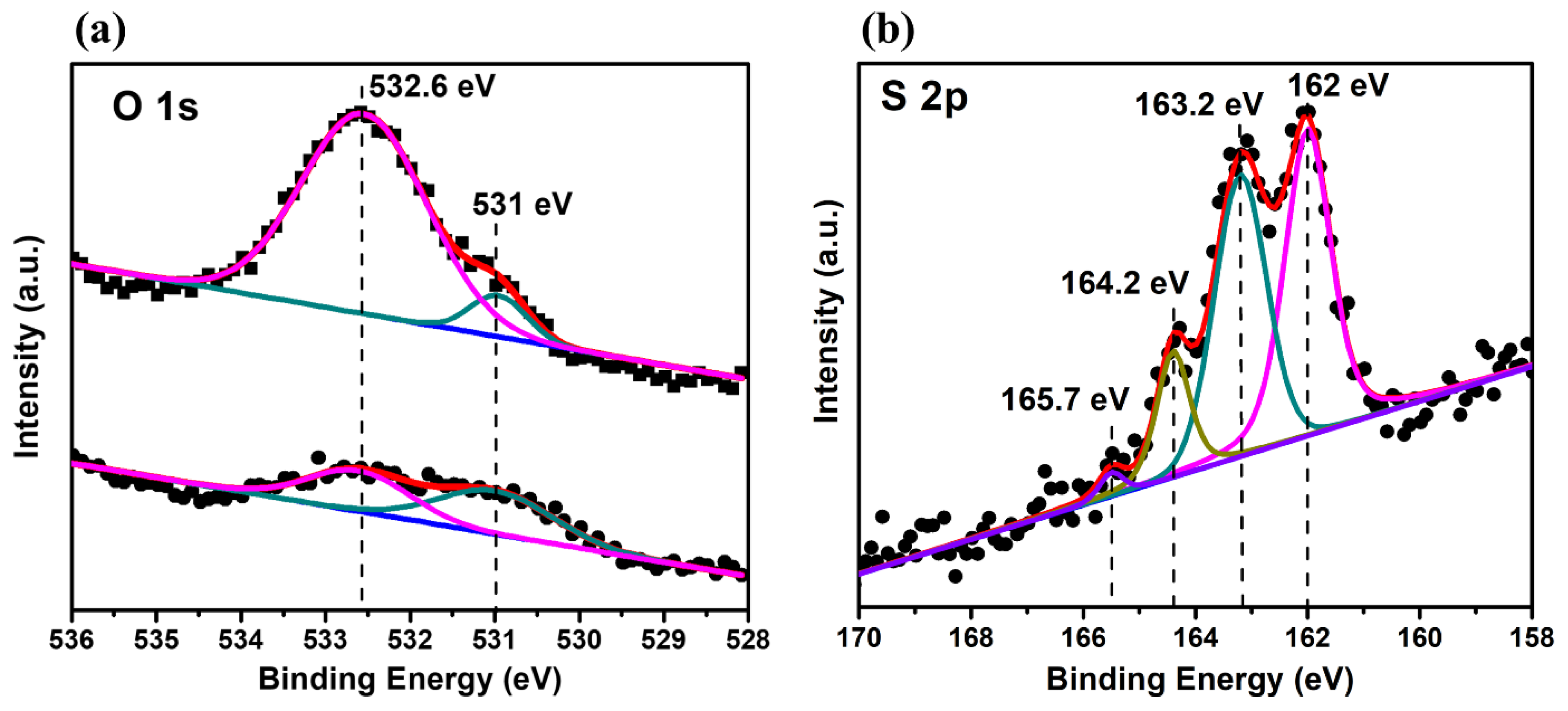
Figure 3.
shows the water contact angles and the angles for precursor solutions, including the SnO2 precursor, perovskite precursor, and spiro-OMeTAD precursor, on bare Au, UV-treated Au, HDT-assembled bare gold, HDT-assembled UV-treated Au, and APTES-assembled ITO.
Figure 3.
shows the water contact angles and the angles for precursor solutions, including the SnO2 precursor, perovskite precursor, and spiro-OMeTAD precursor, on bare Au, UV-treated Au, HDT-assembled bare gold, HDT-assembled UV-treated Au, and APTES-assembled ITO.
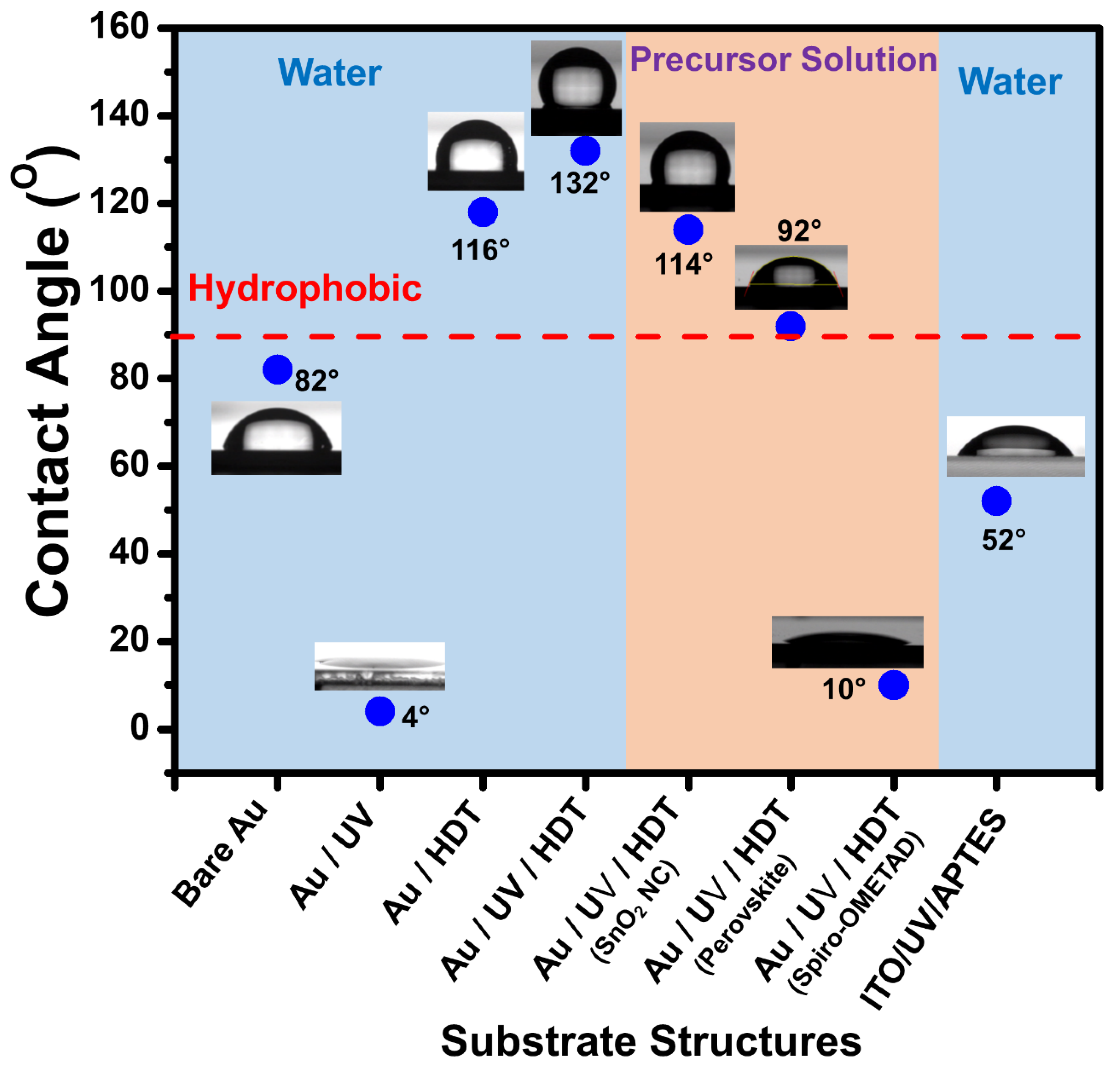
Figure 4.
shows (a) TLM resistance measurements plotted against contact distance d for three different configurations including bare Au/Au, UV-treated Au/HDT SAMs/Au, UV-treated Au/HDT SAMs/Spiro-OMeTAD/Au and (b) a schema of the TLM pattern, where L = 1000 µm, W = 500 µm.
Figure 4.
shows (a) TLM resistance measurements plotted against contact distance d for three different configurations including bare Au/Au, UV-treated Au/HDT SAMs/Au, UV-treated Au/HDT SAMs/Spiro-OMeTAD/Au and (b) a schema of the TLM pattern, where L = 1000 µm, W = 500 µm.
Figure 5.
presents the sequential spin-coating of active layers such as SnO2 NCs and perovskite, on Au/ITO line-space patterns: (a) A schemata of the heterogeneous Au/ITO line-space patterns and optical images showing 9 Au lines; (b) SEM images capturing the selective deposition of active layers on the Au/ITO patterns, line width varying from 50 µm to 1000 µm; (c) Close-up SEM images showing the selective perovskite deposition on ITO and a 200 µm-wide Au line devoid of SnO2 and perovskite with some coatings on the edges. The insets in Figure 5(c) demonstrate a clean Au surface (the left), perovskite microstructures (top on the right), and a wavy Au-perovskite interface (bottom of the right).
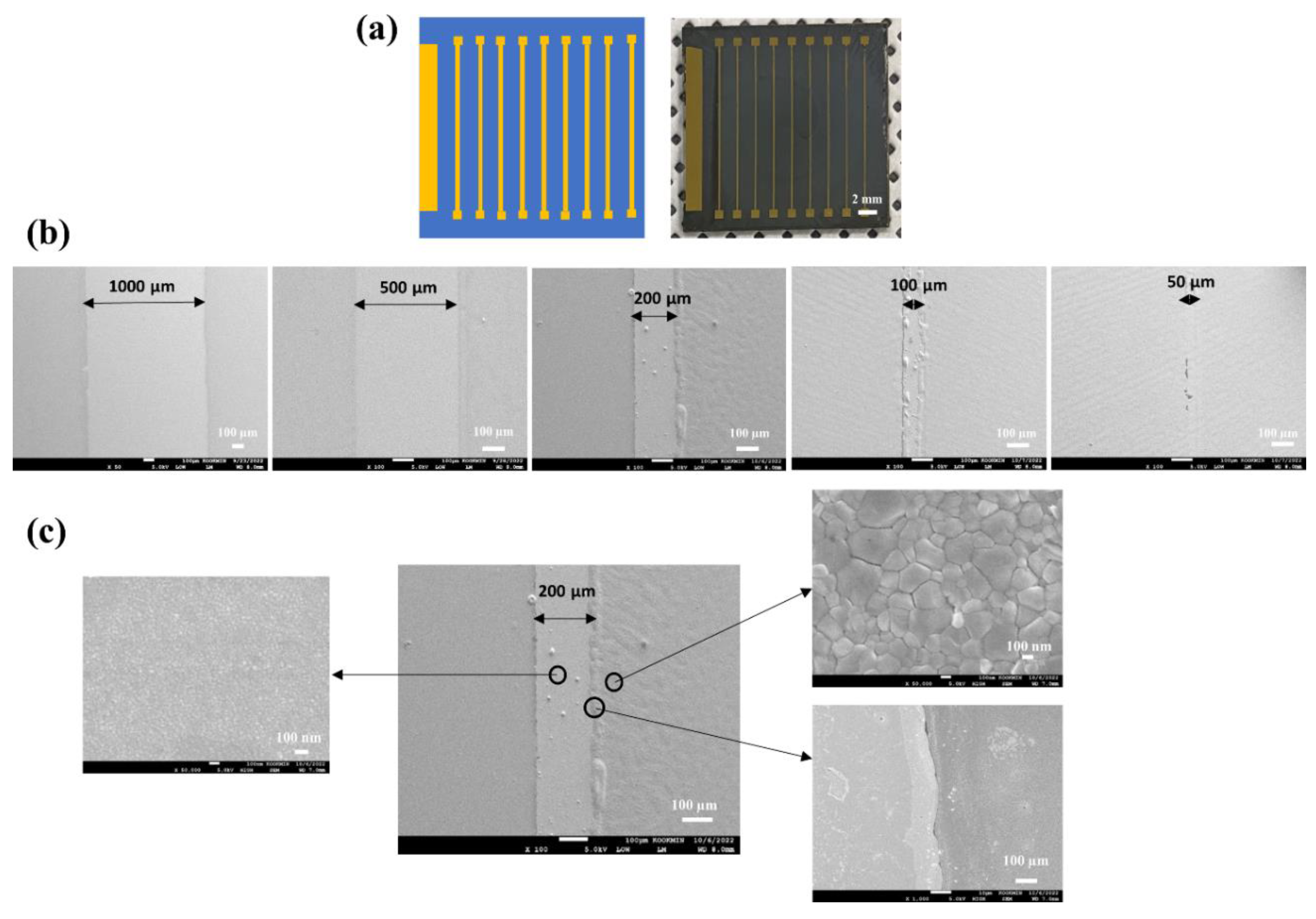
Figure 6.
shows (a) the J-V curve of a single solar cell, which has an average PCE of 13.28%, a Jsc of 22.2 mA/cm2, a Voc of 1.02 V, and a FF of 0.68 under forward bias, (b) the I-V curve of a solar module with six interconnected cells, yielding an average PCE of 8.93%, Voc of 5.39 V, FF of 0.56, and a Jsc of 2.94 mA/cm2. The insets display the optical images of a sample containing four single cells and a solar module with six interconnected cells fabricated based on the selective spin coating-based patterning method.
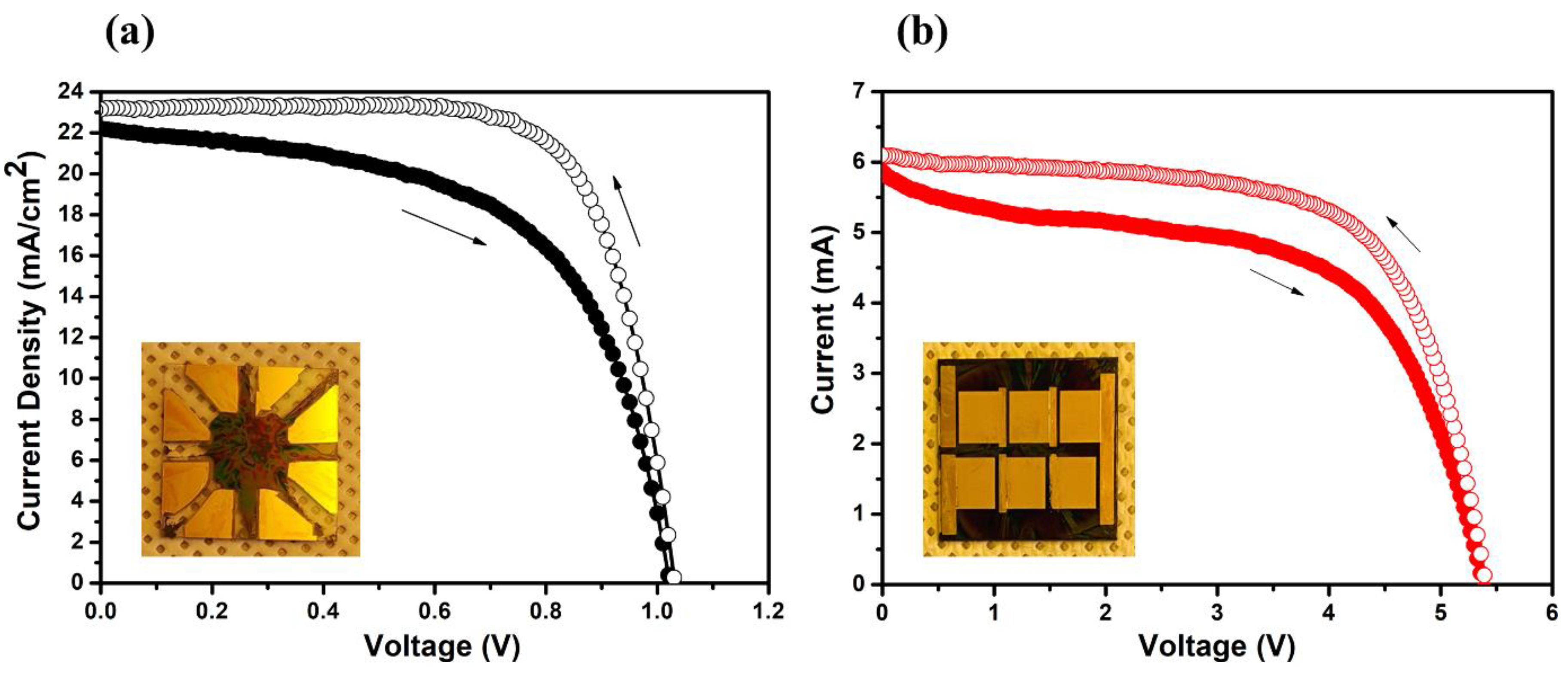

Table 1.
TLM parameters (LT, RSH, RC, ρC) extracted for each contact structure.
| Structure | LT (µm) | RSH (Ω/□) | RC (Ω) | ρC (Ω-cm2) |
|---|---|---|---|---|
| UV treated Au / HDT /Au | 21.7 | 0.46 | 0.02 | 2.17 x 10⁻⁶ |
| UV treated Au / HDT / HTL / Au | 98 | 0.51 | 0.10 | 4.9 x 10⁻⁵ |
Table 2.
Performance parameters of the solar module and the single cell.
| Sample | Jsc (mAcm-2) |
Voc (V) |
FF | PCE (%) |
Rsh (Ω) |
Rs (Ω) |
|
|---|---|---|---|---|---|---|---|
| Single Cell | Forward | 22.2 | 1.02 | 0.58 | 13.23 | 500 | 5.98 |
| Reverse | 23.14 | 1.03 | 0.72 | 17.34 | 1890 | 4.66 | |
| Module | Forward | 2.76 | 5.39 | 0.56 | 8.32 | 600 | 12.31 |
| Reverse | 2.85 | 5.42 | 0.65 | 10.04 | 2381 | 8.24 | |
Disclaimer/Publisher’s Note: The statements, opinions and data contained in all publications are solely those of the individual author(s) and contributor(s) and not of MDPI and/or the editor(s). MDPI and/or the editor(s) disclaim responsibility for any injury to people or property resulting from any ideas, methods, instructions or products referred to in the content. |
© 2024 by the authors. Licensee MDPI, Basel, Switzerland. This article is an open access article distributed under the terms and conditions of the Creative Commons Attribution (CC BY) license (http://creativecommons.org/licenses/by/4.0/).
Copyright: This open access article is published under a Creative Commons CC BY 4.0 license, which permit the free download, distribution, and reuse, provided that the author and preprint are cited in any reuse.


