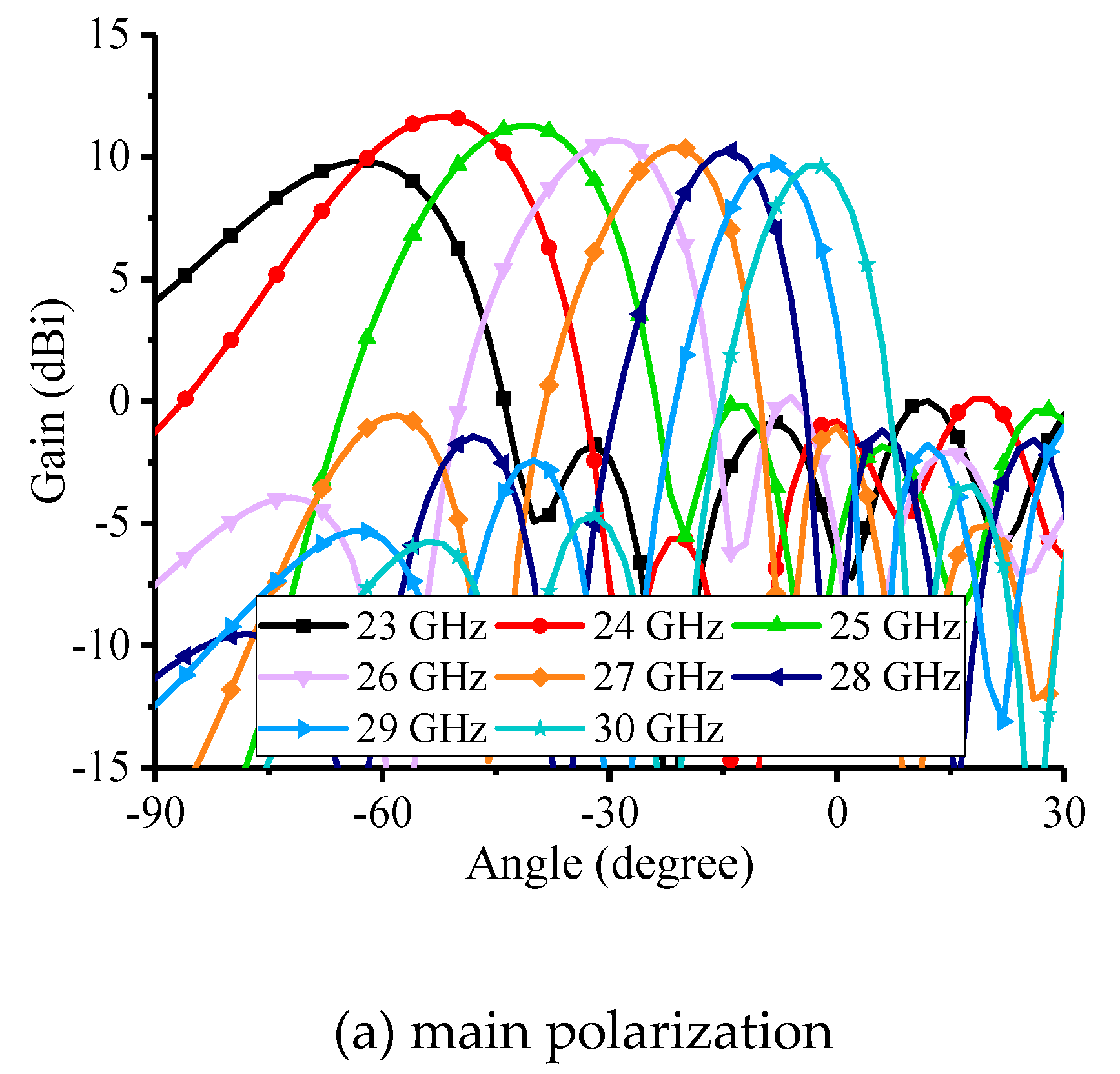
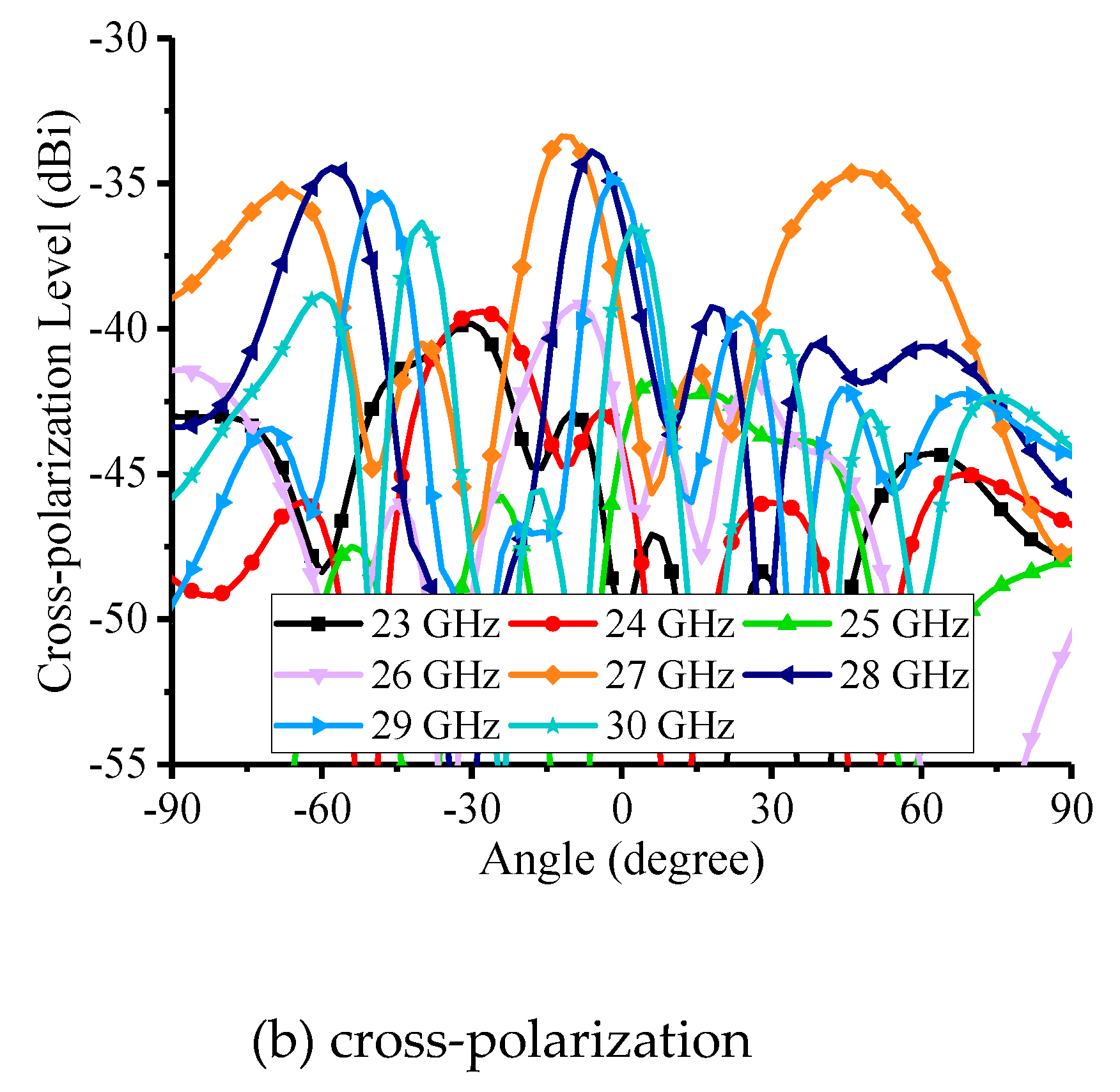
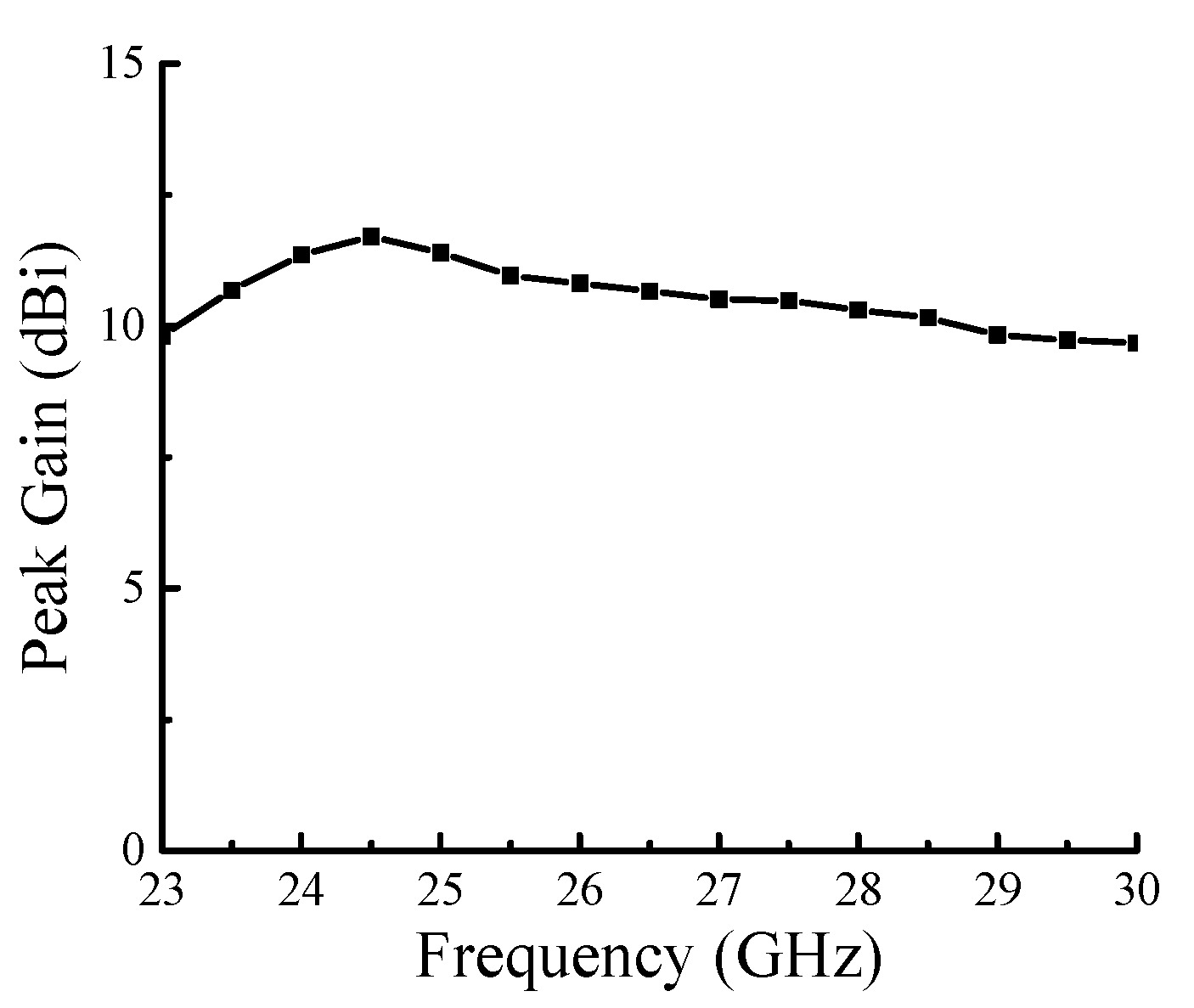
A. Analysis and Design of CSRR-SIW Layer Structure
The Substrate Integrated Waveguide (SIW) is chosen as the feeding transmission line structure, and its cut-off frequency is set as 23 GHz. The SIW is designed using a Rogers RO4003 dielectric substrate with properties of
εr = 3.55, and loss tangent tan
δ = 0.0027, and a thickness of
h1 = 0.305 mm. According to the reference [
15], the calculated equivalent width
weff of the SIW is 3.5 mm, leading to the fundamental dimensions of
vd = 0.4 mm,
vp = 0.7 mm, and
dw = 4.5 mm for the SIW components.
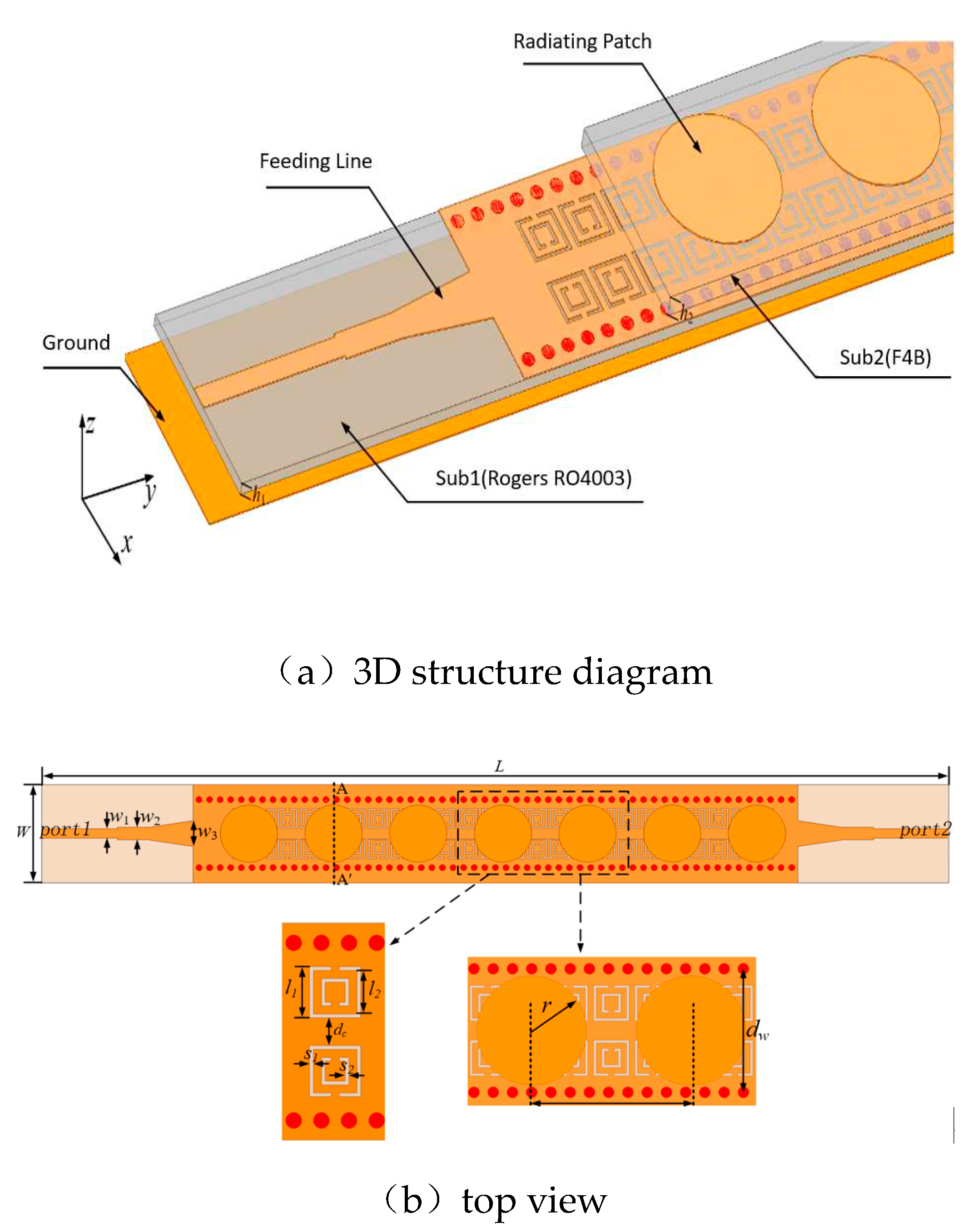
The proposed antenna configuration is depicted in
Figure 1(a) and comprises two distinct layers. The lower layer, referred to as “Sub1”, constitutes the CSRR-SIW layer featuring an open periodic CSRR-type unit slot. For this layer, a Rogers RO4003 dielectric substrate with a thickness of
h1 = 0.305 mm is employed. The Feeding line is structured as a 50 Ω microstrip line, and a specially designed trapezoidal taper structure ensures effective impedance matching between the SIW and the 50 Ω excitation port. On the other hand, the upper layer, labeled “Sub2”", employs circular patches arranged at even intervals to serve as the radiating layer. This layer utilizes an F4B dielectric substrate with properties of
εr = 2.65 and tan
δ = 0.001, and it has a thickness of
h2 = 0.5 mm. The two layers of dielectric substrates are directly connected without any air layer in between, facilitating a tightly integrated antenna structure.
Figure 1(b) illustrates the top view of the designed antenna structure, featuring a CSRR-SIW layer with two CSRR-type radiating slots symmetrically etched above the SIW structure. The effects of parameters such as
l1,
dc,
s1, and
s2 on the transmission characteristics of the CSRR-SIW layer were analyzed using the HFSS simulation software.
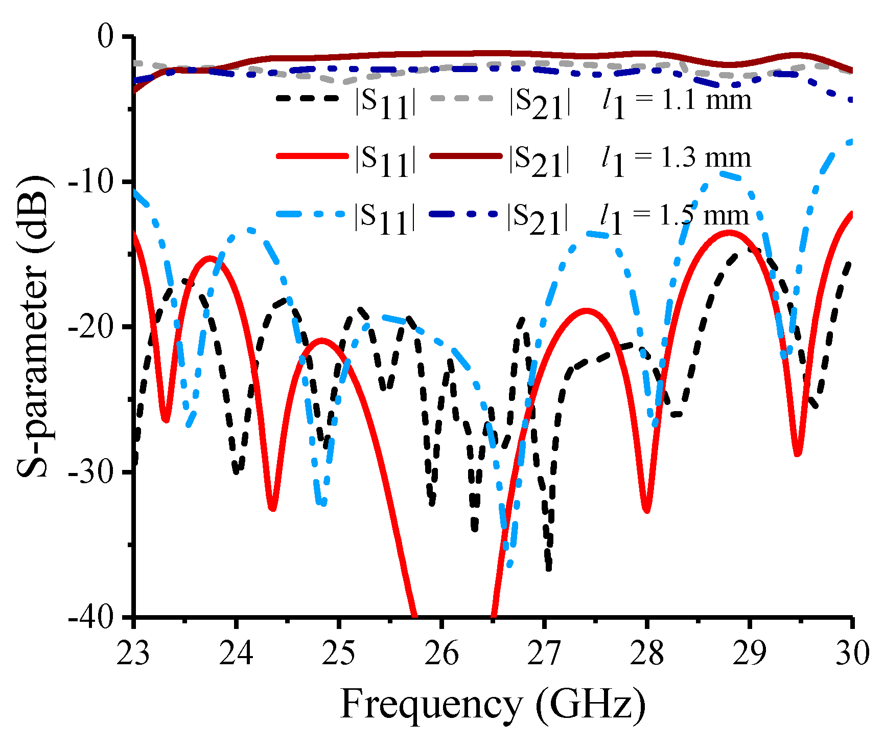
Figure 2 presents the simulated reflection coefficient |S11| and transmission coefficient |S21| of the CSRR-SIW layer, showcasing the relationship with the outer ring metal strip length,
l1. When the other structure parameters remain constant, an increase in the length
l1 of the outer ring metal strip results in a gradual broadening of the matching bandwidth for the CSRR-SIW layer.
The spacing (
dc) between the symmetrically placed CSRR units also plays a significant role in influencing the transmission characteristics of the CSRR-SIW layer.
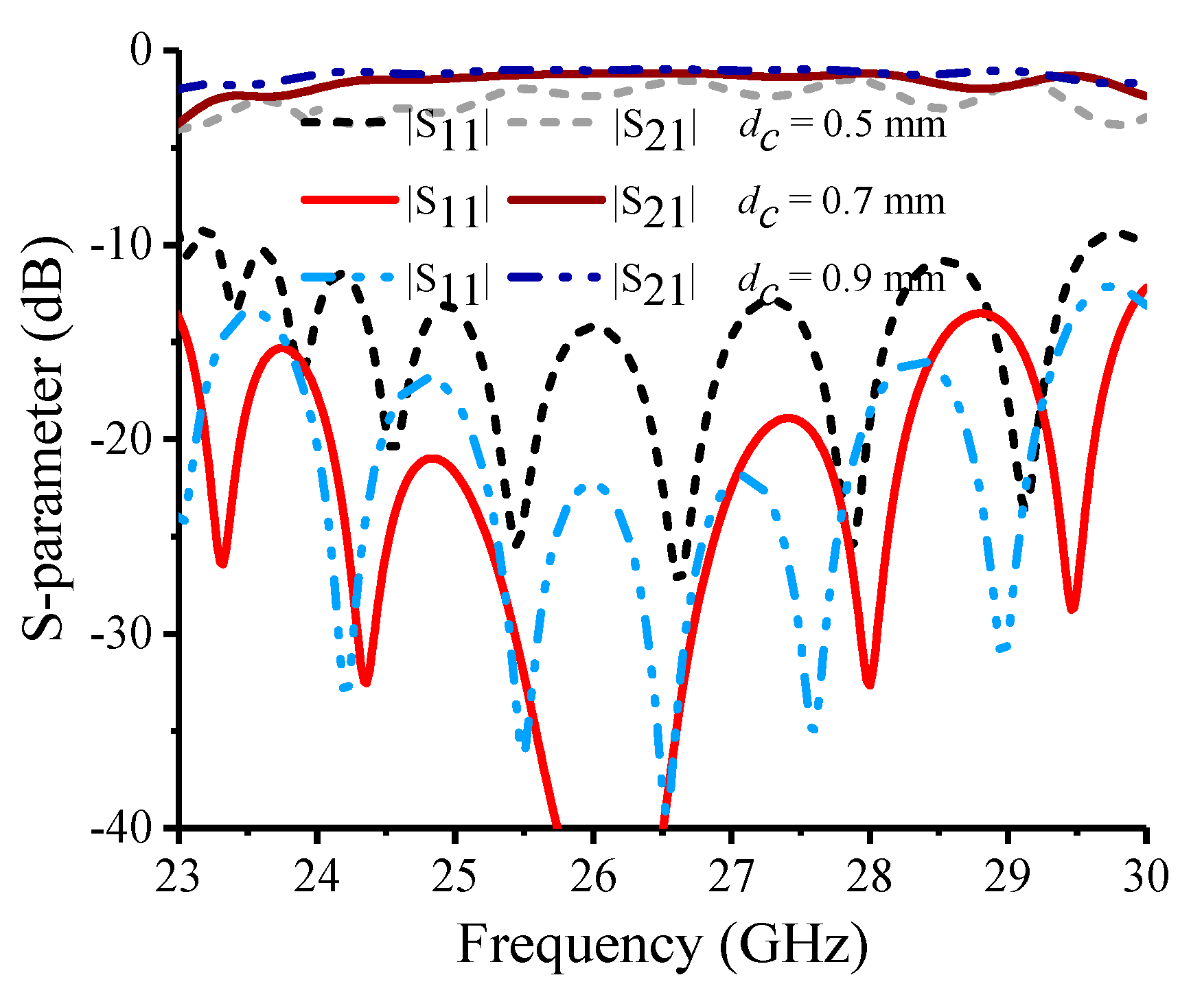
Figure 3 illustrates the impact of the spacing (
dc) on the S-parameters of the CSRR-SIW layer. While keeping the other parameters constant, it is observed that given
dc as 0.5 mm enables the CSRR-SIW layer having a frequency band with |S11| > -10 dB at both low and high frequencies.
As the value of dc is increased from 0.5 mm to 0.9 mm, the reflection coefficient |S11| gradually decreases, leading to a broader matching bandwidth. When dc is chosen as 0.7 mm, |S11| drops below -12.5 dB within the frequency range of 23~30 GHz. This indicates that the CSRR-SIW layer exhibits favorable transmission characteristics at this specific spacing value.
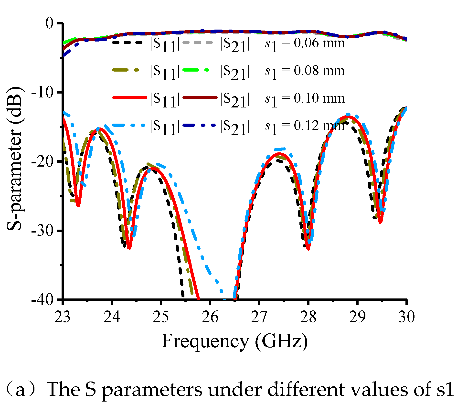
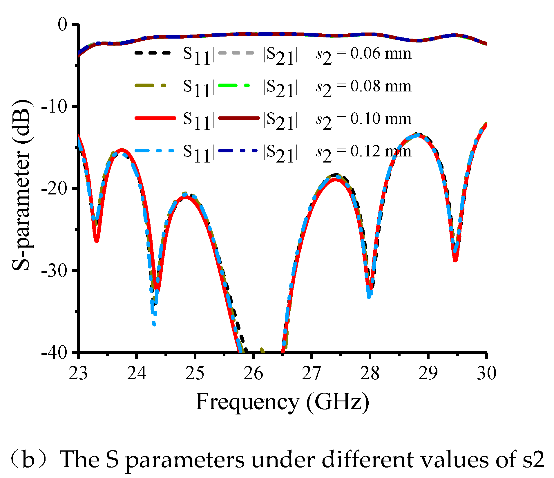
Figure 4 demonstrates the influence of the CSRR inner slot width (
s1 and
s2) on the S-parameters of the CSRR-SIW layer. While maintaining the other parameters constant, it can be observed that as the values of
s1 and
s2 increase from 0.06 mm to 0.12 mm, the curves of |S11| and |S21| exhibit only minor fluctuations. This suggests that
s1 and
s2 have minimal effects on the transmission characteristics of the CSRR-SIW layer.
Therefore, when the waveguide width (dw) of SIW remains unchanged, the primary factors affecting the transmission characteristics of the CSRR-SIW layer are the length l1 of the CSRR unit edge and the spacing dc between the symmetrically placed CSRR units. Other parameters, such as s1 and s2, have a relatively limited impact on the overall performance of the CSRR-SIW layer in terms of S-parameters.
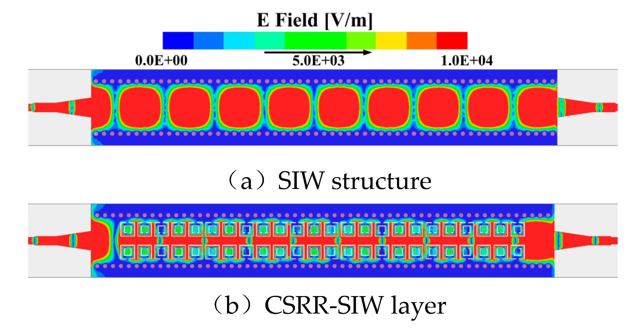
In
Figure 5, the electric field distribution of two structures, namely an SIW and a CSRR-SIW layer with etched CSRR-type slots of the same size, is presented at the central frequency of 26.5 GHz. It is evident that the SIW structure operates in the TE
10 mode, displaying eight electric field periods inside the waveguide.
On the other hand, the CSRR-SIW layer exhibits nine electric field periods, indicating that its waveguide wavelength is shorter, leading to a larger phase constant. This observation confirms that the slow-wave characteristics of the SIW structure are enhanced by etching CSRR-type slots on the surface of the SIW. The presence of the CSRR-type slots introduces additional periodicity, resulting in a shorter wavelength and larger phase constant, thus validating the improved slow-wave behavior in the CSRR-SIW layer compared to the standard SIW structure.
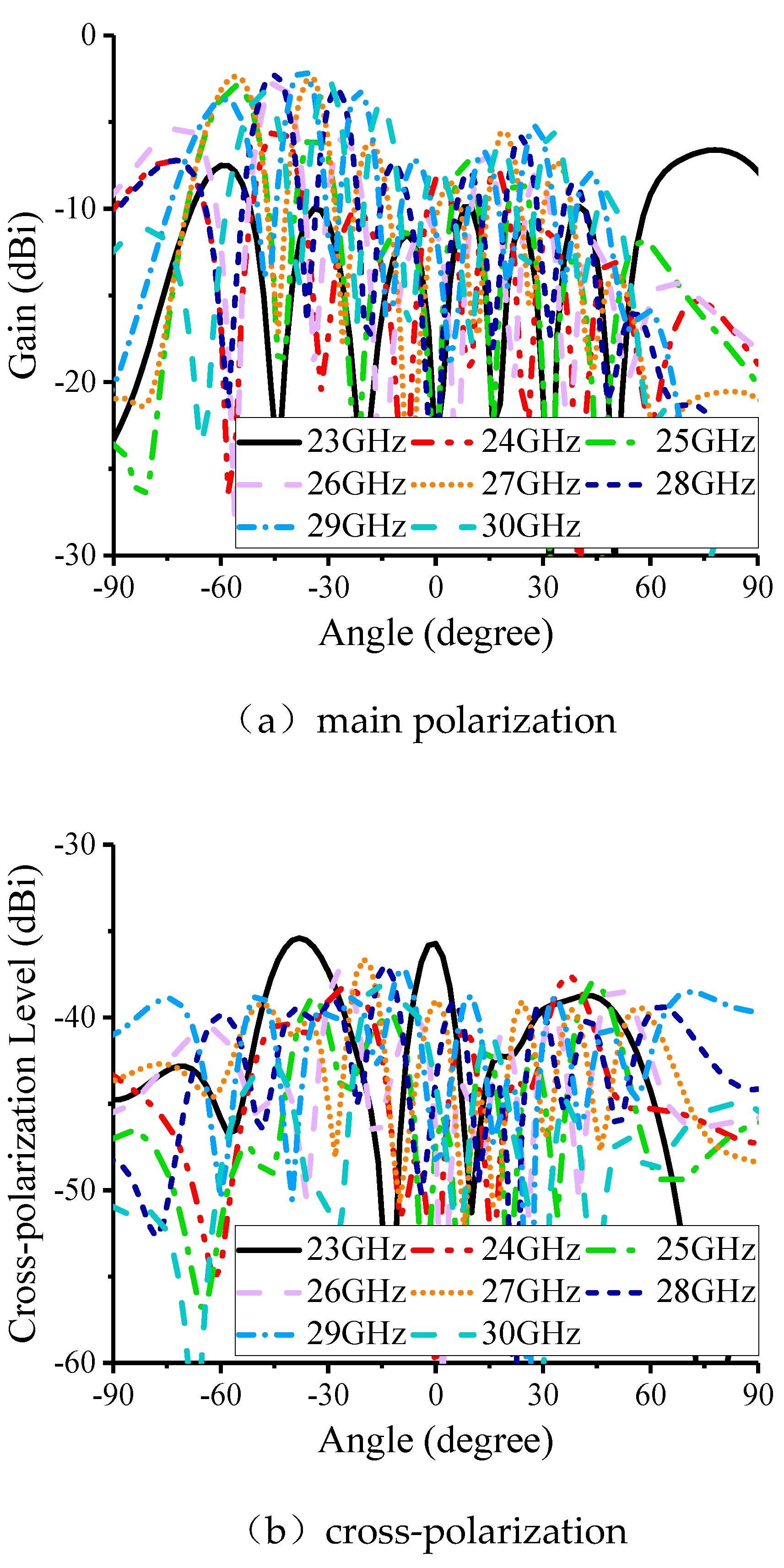
In
Figure 6, the radiation pattern of the CSRR-SIW layer is depicted. The polarization pattern shown in
Figure 6(a) indicates that the CSRR-SIW layer does not possess frequency scanning functionality within the frequency range of 23~30 GHz. Furthermore, the maximum gain in the main polarization direction is merely -2.5 dBi, and the cross-polarization level is below -35.4 dBi.
Based on the analysis of the structural parameters of the CSRR-SIW layer and the observation of the electric field distribution, it can be inferred that the CSRR-SIW layer primarily functions in transmission and feeding roles. To achieve electromagnetic energy radiation effectively, additional radiation elements need to be integrated into the structure. The current CSRR-SIW layer acts as a transmission medium rather than an active radiating element, contributing to the overall functionality of the antenna structure.
B. Antenna Performance Analysis
Circular patches are widely used as radiating elements in antenna design due to their straightforward structure, and they are particularly common in microstrip patch antennas. The fundamental mode of circular patches is the TM
11 mode. The radius (
r) of the circular radiating patch can be approximately calculated using the following formula [
16]:
In this paper, the circular patches are arranged in the upper layer to form an equidistant linear array, with a total of 7 circular patches. The spacing between adjacent patches is set to dr = λg/2 = 5.6 mm, where λg represents the waveguide wavelength calculated using formula (6).
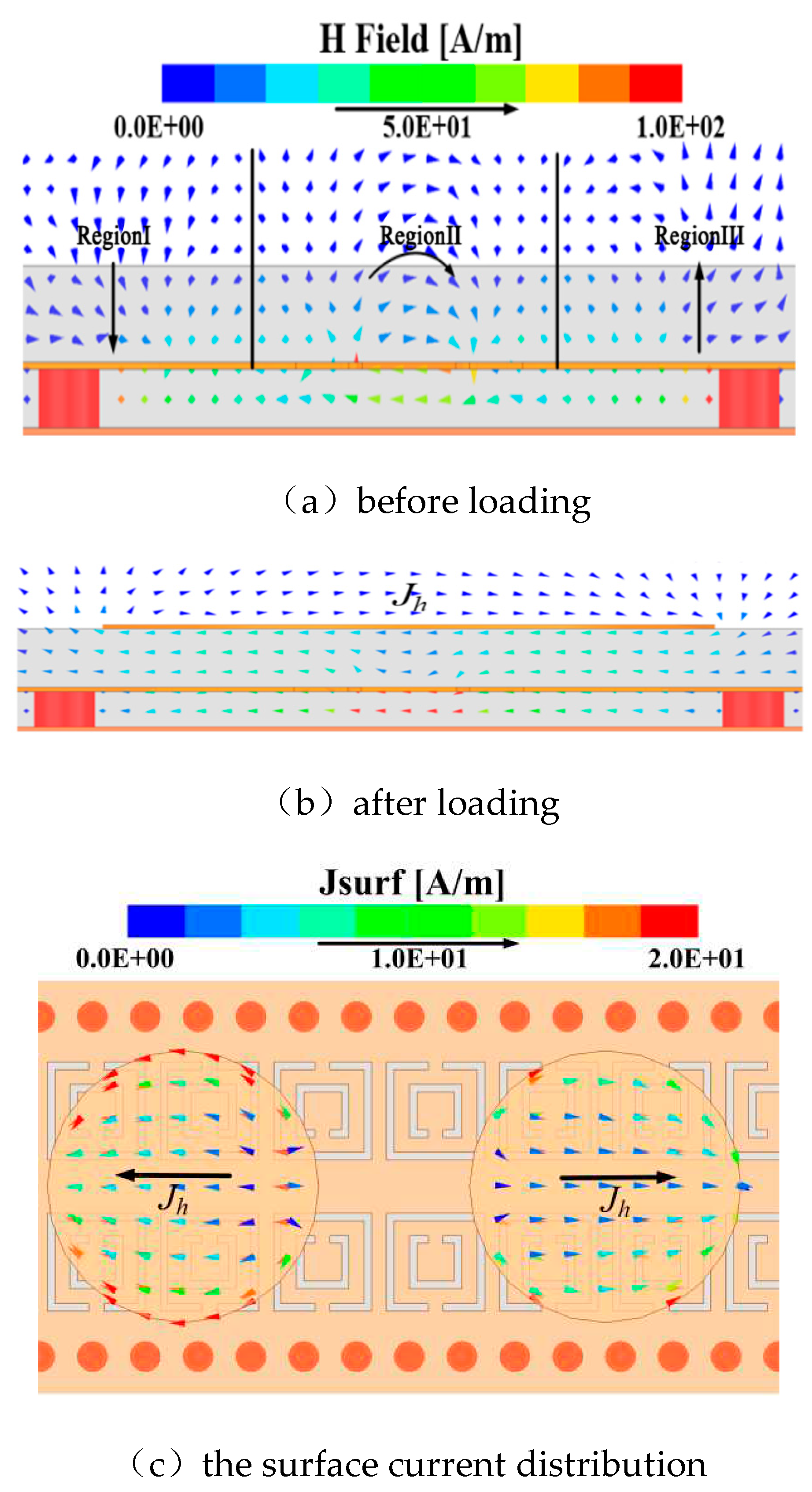
In
Figure 7(a) and (b), the magnetic field distribution on the AA' plane of the CSRR-SIW layer is illustrated before and after loading the radiating patches, respectively. At the frequency of 26.5 GHz, in the absence of the radiating patches, the magnetic field is tightly confined to the SIW layer, and magnetic coupling occurs between the symmetrically placed CSRR units. Consequently, the magnetic field distribution above the SIW layer gradually weakens.
Via loading the radiating patches, a notable interaction arises between the out-of-phase magnetic field components in regions I and III and the radiating patches. This interaction induces a horizontal induced current (Jh) on the surface of the radiating patches.
The introduction of the radiating patches alters the magnetic field distribution, leading to the creation of induced currents on the patches’ surfaces. These induced currents contribute to the radiation of electromagnetic energy, enhancing the overall performance of the antenna by providing radiation capabilities that were absent in the initial CSRR-SIW layer configuration. The induced horizontal current (
Jh) flows along the surface of the metal patches, resulting from the interaction between the out-of-phase magnetic field components in regions I and III and the radiating patches. This current significantly enhances the magnetic field in regions I and III compared to the situation without the patches. This enhancement indicates a strong coupling between the radiating patches and the energy radiated by the SIW in the lower layer. The current distribution as shown in
Figure 7(c) is horizontal along the surface, indicating that the antenna radiates horizontally polarized waves. The induced current on the circular radiating patches facilitates the emission of electromagnetic energy in a horizontal polarization, making the antenna suitable for radiating horizontally polarized signals. This is a desirable characteristic for many communication applications.
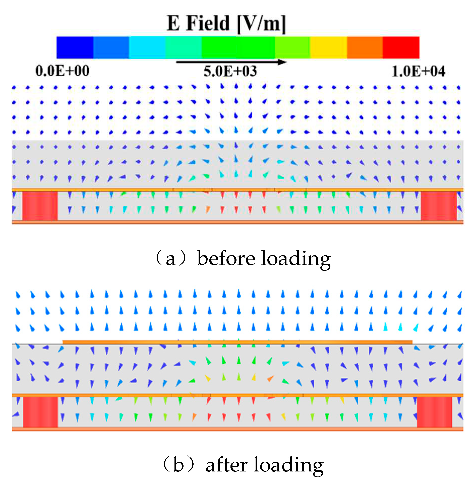
Based on the analysis discussed earlier, the magnetic field coupling within the structure leads to the radiation of horizontally polarized waves. However, to achieve high purity of horizontally polarized waves, it is necessary to suppress electric field coupling.
Figure 9 illustrates the electric field distribution on the AA' plane before and after loading the circular radiating patches at the frequency of 26.5 GHz. It’s shown that there is no significant change in the electric field distribution on the AA' plane before and after loading the patches. This lack of change indicates that the electric field coupling has been effectively suppressed. By mitigating electric field coupling, the antenna can achieve a high level of purity in the horizontally polarized waves, ensuring improved performance for specific applications that require high cross polarization ratio.
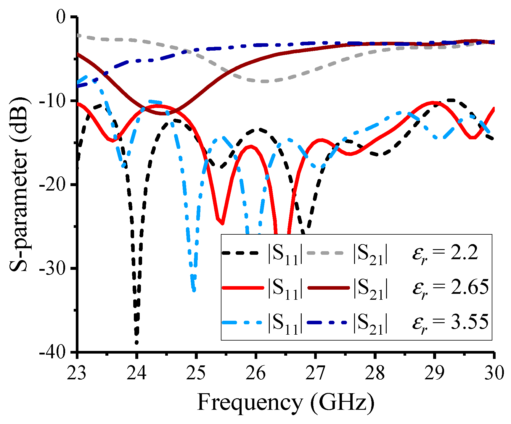
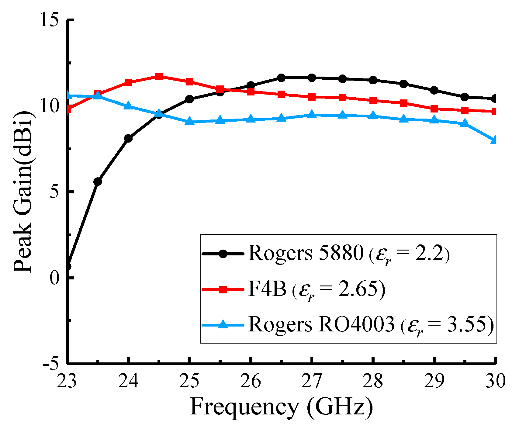
The impact of different upper-layer substrate materials with varying relative permittivity (
εr) on the overall antenna structure's S-parameters and peak gain was analyzed.
Figure 10 and
Figure 11 display the simulated S-parameters and peak gains of the various antenna structures using different upper-layer substrate materials: Rogers RT5880 with
εr = 2.2, F4B with
εr = 2.65, and Rogers RO4003 with
εr = 3.55 (the same material as the CSRR-SIW layer). From the analysis of
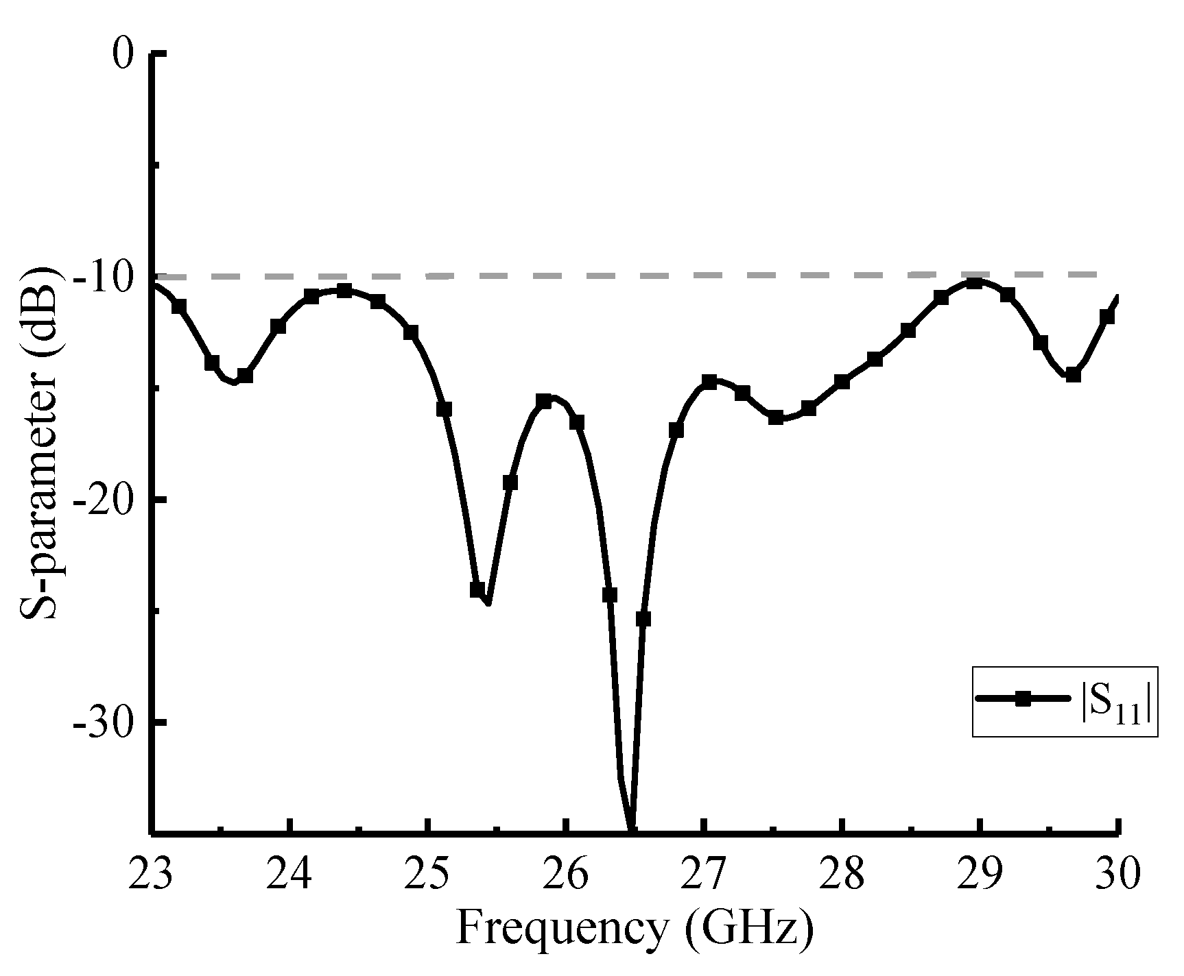
Figure 10, it becomes evident that as the relative permittivity of the upper-layer substrate decreases, the matching bandwidth with |S11| < -10 dB gradually widens, particularly at lower frequencies. Additionally, the minimum position of the |S21| curve shifts towards higher frequencies as
εr decreases.
Turning to
Figure 11, it demonstrates that when using a substrate material with
εr = 2.2, the peak gain exhibits more significant fluctuations, while using a substrate material with
εr = 3.55 leads to a lower gain. The reduced gain in the latter case can be attributed to increased losses at higher frequencies due to the higher permittivity of the substrate.
Based on these observations, the upper-layer substrate material with εr = 2.65 (F4B) is chosen for the radiating layer. This selection is made to achieve a balance between wider bandwidth with good matching and a stable peak gain performance. The chosen substrate material ensures efficient radiation with reduced losses at higher frequencies, making it the optimal choice for the specific application of the antenna.
