
Submitted:
13 November 2023
Posted:
14 November 2023
You are already at the latest version
Abstract
Point-contact spectroscopy has been performed on bulk samples of electron-doped high temperature superconductor Nd2-xCexCuO4-. The samples were characterized by X-ray diffraction and scanning electron microscopy equipped with a wavelength dispersive spectrometer and an electron backscatter diffraction detector. The samples with a Ce content x = 0.15, show the absence of spurious phases and randomly oriented grains, most of which have dimensions of approximately 220 µm2. The low-bias spectra in the tunnelling regime, i.e., high transparency interface, exhibit a gap feature at about ±5 meV and no zero-bias conductance, consistent with the most literature data on oriented samples. The high-bias conductance has also been measured in order to obtain information on the properties of the barrier. A V-shape has been in some cases observed, instead of the parabolic behavior expected for tunnel junctions.
Keywords:
electron-doped cuprates
; point-contact spectroscopy
; tunnelling
1. Introduction
It is well known that point contact spectroscopy (PCS) can give insight into the size and the nature of superconducting energy gap. This technique has been widely used on conventional as well as new generation superconductors [1,2,3,4,5,6]. By changing the pressure between a tip made of normal metal (N) and a superconducting sample (S), it is possible to obtain different types of contacts, i.e., different electrical transport regimes that depend on the nature of the interface. Both quasiparticle NIS junctions (here I stands for insulating barrier) and NS contacts obtained through PCS can be used to study the energy gap in superconductors [7]. By changing the tip position on the surface of a polycrystalline sample, with random oriented crystallites, different tunnelling direction with respect to the crystallographic orientation of the crystalline grain can be investigated, thus providing information on the anisotropy of the superconducting order parameter and the possible presence of nodes as in d-wave symmetry of the superconducting order parameter.
Among high-temperature superconductors, electron-doped copper oxides, with the chemical formula RE2-xCexCuO4 (RE= Pr, Nd, Sm, La), have also been investigated by PCS. As in the case of the hole-doped high-Tc cuprates, the phase diagram of electron-doped cuprates shows a well-known ‘dome’ shape with the highest Tc at a doping level of about 0.15, but with a superconducting window much narrower and an antiferromagnetic phase that persists at higher doping levels [8,9,10,11]. Several techniques have been used to investigate the electronic properties of electron-doped superconductors, including Angle Resolved Photoemission Spectroscopy (ARPES), tunnelling spectroscopy, magnetic penetration depth measurements, and transport measurements. ARPES measurements have revealed the presence of multiple bands in the electronic structure [12,13,14,15,16,17,18,19,20,21,22]. In particular, the over-doped region is characterized by a large hole-like Fermi surface that undergoes a Fermi surface reconstruction at intermediate doping levels with the presence of electron and hole pockets. In contrast, only electron pockets are present in the underdoped region.
Superconducting and normal state properties of electron-doped cuprates have been extensively investigated by resistivity, magneto-transport and Hall effect measurements. In particular, the sign change of the Hall coefficient measured in cerium over-doped samples has been described as evidence of the presence of two types of charge carriers, electrons and holes, as also supported by the ARPES experiments, and the appearance of superconductivity has been related to the presence of holes [23,24,25,26,27,28,29,30].
As revealed by tunnelling experiments and magnetic penetration depth measure-ments, the symmetry of the superconducting order parameter in electron-doped cuprates has been more controversial, unlike hole-doped cuprates for which the pairing symmetry is predominantly d-wave. Several experimental data on n-type samples are consistent with an order parameter having a d-wave symmetry, [13,14,19,20,22,31,32]. However, many tunnelling experiments showed no evidence of a zero bias conductance peak (ZBCP), expected for a d-wave superconducting system, suggesting a pairing symmetry of the s-wave type. Furthermore, PCS experiments on Pr2-xCexCuO4 at different Ce doping level have shown evidence of ZBCP in underdoped samples suggesting a change of symmetry with doping, from d to s-wave with increasing doping [28,32,33,34,35]. The absence of ZBCP has been also attributed to the coexistence of antiferromagnetic and superconducting orders [36]. Magnetic penetration depth measurements on Pr2-xCexCuO4 and La2-xCexCuO4 (RE = Pr, La) films at different Ce content also suggested a d-wave to anisotropic s-wave transition across the optimal doping [37,38]. A two-band model with d-wave pairing symmetry and different doping-dependent amplitudes has been successful used to describe the magnetic penetration depth measurement and Raman experiments on electron-doped cuprate superconductors [26,27].
Among cuprates, electron-doped oxides do not show a strong pseudogap at the antinodal region. This constitutes an advantage in the investigation of the superconducting gap, which is relatively small. In the past, various studies have shown that the superconducting pairing strength is close to a weak-coupling regime, at least in the optimally doped and over-doped region [31,39]. The study of the superconducting density of states with the energy gap is performed through low bias conductance measurements. On the other hand, the normal state can be also investigated, by means of the high bias conductance measurements. In the past, a linear background conductance has been observed in many HTS compounds and related to the normal density of states of the cuprate superconductors. This behavior has been ascribed to the interlayer coupling mechanism between the CuO2 planes [40].
In this work, we report PCS measurements on optimally doped Nd2−xCexCuO4−δ bulk samples. Differential conductance of tunnel junctions with different contact resistances have been acquired. Differential conductance at low bias shows the presence of superconducting gap structures at ±5 meV consistent with the values already reported in literature. The temperature dependence of the conductance shows well defined gap structures up to 15 K, above this temperature the conductance flatness and the gap closes as expected for a superconducting gap. The paper is organized as follows: Section 2 describes the experimental details of fabrication and characterization of our bulk samples of Nd2−xCexCuO4−δ compound. In Section 3 the Blonder, Thinkam and Klapwijk (BTK) theory of point contact spectroscopy is briefly summarized. Section 4 reports our results on point contact measurements and the related discussion. Finally, Section 5 presents our conclusions.
2. Samples Characterization
In Nd2−xCexCuO4−δ samples, the superconductivity occurs in a narrow range of Ce doping: 0.10 - 0.24 with the highest Tc = 24 K at a doping level of about 0.15.
Unlike hole doped HTS, for electron-doped compounds not only doping is required, but a proper oxygen-reducing process is essential to observe superconductivity [8,9,41]. The role of this reduction process is a long-standing issue on electron-doped high temperature superconductors. Indeed, the as-grown samples do not show superconductivity, and it is necessary to perform a thermal treatment in low oxygen environment and at high temperatures, to drive the samples in the superconducting state. This reduction process affects the amount of oxygen atoms and their distribution in the crystalline structure and significantly impacts the transport and magnetic properties of the samples, transforming them from antiferromagnetic semiconductors to superconducting metals [42,43,44,45,46,47,48,49].
The electron doped compounds crystallize in a T’ crystal structure with one square planar copper-oxygen CuO2 layer in between charge reservoir layers and characterized by the absence of oxygen ions at apical sites (above and below CuO2 layers).
Recently, experimental, and theoretical finding on as-grown oxygen-deficient Nd2−xCexCuO4−δ films suggested a structural reorganization involving the oxygens ions at apical positions, which remodulates the electronic band structure. No apical oxygens, or too many of them, stabilize strong antiferromagnetic correlations, whereas an intermediate number of apical oxygens suppresses antiferromagnetic correlations and allows to have holes available at the Fermi level. This is consistent with the presence of both holes and electrons in the superconducting samples, as revealed by many experiments [50,51,52,53,54,55].
Bulk samples of Nd1.85Ce0.15CuO4 (NCCO) were synthesized by standard solid state reaction technique. To remove carbon dioxide and moisture, a pre-calcination was done on Nd2O3 and CeO2 for about 10 h at 950 °C. Afterwards, a stoichiometric amount of 4 N purity Nd2O3, CeO2 and CuO were weighed and grinded in an agate mortar using acetone as a binding agent. After calcinations in air at 1020 °C for 24 h, the samples were reground, pressed into pellets, and sintered in air at 1150 °C for 24 h. Finally, a reduction process at 900 °C for 30 h in argon atmosphere was carried out to observe the superconducting transition [56].
X-ray diffraction measurements confirmed the crystalline quality and the phase purity of the final sample. Figure 1 reports an example of diffractogram of the powder obtained from our NCCO after all the thermal treatments: by using X’Pert HighScore software we found a perfect match of our diffractogram with the reflections of the tetragonal NCCO phase with space group I4/mmm (ICDD 01-080-1645) and cerium content of 0.15.
The chemical composition of the samples was studied by a scanning electron microscope (SEM) equipped with a wavelength dispersive spectrometer (WDS) and the measurements confirmed that the cerium content is 0.15. The possible presence of some spurious elements was checked by WDS scans on the whole surface in a range of wavelengths going from 1.14 to 175 Å. The results obtained on one of the samples are shown in Figure 2 for a reduced wavelength range, from 1.14 to 30 Å. In this range all the peaks can be attributed to X-ray reflections from Nd, Ce, Cu and O, which are elements of the compound. The scan performed on all the samples in the whole range, i.e., up to 175 Å, revealed no trace of spurious elements within the experimental error.
A grain analysis was performed on these pure and stoichiometric samples by using electron backscattered diffraction (EBSD) measurements, carried out with a SEM LEO-EVO 50 equipped with an INCA Crystal 300 EBSD system. The electron beam scans a flat selected area of the sample, properly prepared by metallographyc techique (diamond pastes down to 1 μm), and the diffracted x-rays are collected in a pattern on a phosphore screen showing the so called Kikuchi bands. The sample is mounted on a special stub, tilted of 70° with respect to the orizohontal plane, where three directions are defined as reference for the orientation of the sample: the sample normal (SN) is perpendicular to the sample surface, the rolling direction (RD) and the transverse direction (TD) are in the sample’s plane, and they are perpendicular each others and with respect to the SN. The software identifies in its database what phase the pattern corresponds and what orientation has the crystalline cell for each pixel of the SEM image. The different orientations are highlighted according to a colour-coded stereographic triangle related to the phase added in the database. In Figure 3 a SEM image of a metallographically prepared (diamond paste down to 1 µm) polycrystalline sample in the EBSD configuration is shown together with the orientation references. The inverse pole figures reported below for each reference denote the polycrystalline nature of the sample: in fact, the random distibution of the intensities in the three pole figures points out that no preference orientations are detected.
The Figure 4 reports the SEM image of the same sample with its superimposed orientation map: several grains are detected with different orientations, i.e., different colors in the map, according to the colour code key of the NCCO phase. The histogram on the right plots the number of grains detected in the orientation map as function of their dimensions; it results that the majority of grains has size of about 220 μm2. In order to evaluate the misorientation among the several grains, a grains map was analysed. Figure 5 shows this kind of map of the sample around one of the larger grain. In this map, at each grain is assigned a discrete colour to differentiate it from the neighbouring grains. Right panel of Figure 5 represents the changes of the misorientation angles for the different profile scans highlated in the map. The sharp profiles suggest that even the grains with larger misorientation result strongly interconnected without exhibiting spurious phases at the interfaces, as also confirmed by compositional SEM analysis (not reported here).
From the EBSD analysis it is clear that the sample is polycrystalline and it is not possible to identify a preferential orientation of the grains (see Figure 3). Looking at the orientation map along the normal direction reported in Figure 6a), each color in the map corresponds to a specific orientation of the crystalline cell for that grain taking into account the reference color key (Figure 6b)). As an example, the red grains are oriented with the c-axis perpendicular to the surface of the sample, the green ones have the a-axis perpendicular to the surface, and so on. Even if there is no preferred orientation, a graphical analysis of the orientation map image along the normal direction could give some information on the number of pixels with a certain color. Since groups of red pixels, as an example, correspond to one or more grains with a certain orientation, a statistic on the number of red pixels can be considered a statistic on the orientation of the grains. In the map of Figure 6a) can be clearly distinguished red, green and blue pixels corresponding to [001], [100] and [110] directions, respectively. By selecting red, green or blue channel in the graphic software, the histograms report the color intensity related to the particular channel with a media value around the maximum of the intensity, as shown in Figure 6c). Even if there is no preferential orientation among the grains of our sample, on average, the red histogram shifted towards higher mean intensity, can be interpreted as a greater number of grains having a significant component in the [001] direction, compared to the other orientations.
3. Theory
When a point contact is realized between a superconductor (S) and a normal metal (N), a small contact area will form, giving rise to an NS junction. Andreev’s reflections (AR) may occur when an electron in N incident at the interface has an energy lower than the S energy gap, forming a Cooper pair which can enter in S leaving a hole in N. The AR is then a retroreflection of a hole of opposite spin and velocity but momentum equal to the incident electron. From an experimental point of view, the formation of Andreev bound states are seen in the differential conductance spectra as a peak at zero bias. In fact, a net charge transfer of 2e will occur from N to S in the high transparency (i.e., transmission coefficient) limit; the conductance of the junction, when all electrons incident at the NS interface with energy lower than the superconducting gap are subject to AR, will be twice the conductance of the normal state [57,58]. The transparency of the interface can be however changed, by changing the distance and/or pressure tip/sample in this way giving rise to different electrical transport regimes. It is so possible to make a combination of point contact and barrier type junctions by using PCS, realizing different kinds of contacts. In particular, when the transparency is low enough, a tunnel junction will be obtained, which is usually indicated as an NIS junction where I stays for the insulating barrier.
The tunnel current in junctions made by two different materials can be written as [7]
Here, ρ1(E) and ρ2(E) are the quasiparticle DOS in the two electrodes, f(E) is the Fermi–Dirac distribution function which describes thermal smearing, and GNN = RNN is the junction conductance when both electrodes are in the normal state.
For a normal metal-insulator-supercondutor (NIS) junction where electrode 1 is a normal metal, ρ1(E) = 1, and electrode 2 is a superconductor with a DOS ρ(E), in the limit T = 0 K, the tunnelling conductance dI/dV becomes
Here we assumed E = eV. The bracketed function is sharply peaked with half-width 3.5 kBT, so in the limit of T = 0 K
The superconducting DOS at T = 0 K can thus be obtained from the ratio of the tunnelling conductance when one of the electrodes is in the superconducting state to the tunnelling conductance when both electrodes are in the normal state.
The theory of superconductivity by Bardeen, Cooper and Schrieffer (BCS) [59] predicted a characteristic DOS structure:
where Δ is the energy gap. An exact determination of ρ(E) requires a measurement of normal state (background) conductance GNN. While GSN is readily measured at T « TC, the measurement of GNN can be difficult. It is possible to introduce a magnetic field to quench the superconductivity, or to raise the temperature above Tc. However, a background shape can be drawn from high bias conductance and used to normalize the measured overall conductance.
Both quasiparticle NIS junctions and NS contacts obtained through PCS can be used to study the energy gap in superconductors [7]. For the general case of a junction between N and S, with or without insulating barrier, the differential conductance can be expressed by means of the Blonder, Thinkam and Klapwijk (BTK) [60] theory:
The Z parameter modulates the interface between N and S. The case Z = 0 corresponds to a NS junction, with a completely transparent barrier, in which the dominant mechanism responsible for the transport current is the Andreev process. In this case, Andreev reflections (AR) can constitute the predominant process at the interface and the shape of the conductance is different, showing the so-called zero-bias anomaly (ZBA), hallmark of AR [61].
On the other hand, Z > 1 represents a junction with low transparent barrier, corresponding to a dominant tunnelling current flowing through the junction, in other words a NIS junction. A(E) represents the Andreev reflection probability and B(E) represents the normal reflection probability.
The BTK theory can be extended to the case of unconventional superconductors with different symmetries of the order parameter (OP). In this case the normalized conductance at T = 0 K is written as:
where is the incident angle of the quasiparticle and α is the angle between the crystallographic a-axis and the normal to the tunnelling interface, and E = eV, with V being the bias voltage. For isotropic s-wave order parameter , while in the case of a d-wave symmetry . Figure 7 shows the normalized conductance at T = 0 K and with Z = 5 (tunnelling regime) in the case of isotropic s-wave symmetry, panel a), and for d-wave symmetry with and , panel b), c) and d) respectively. The ZBA could also be originated by a d-wave order parameter as shown in Figure 7 panels c) and d).
In order to account for the often-observed asymmetric background conductance, a generalization of the BTK theory has been proposed, including three regimes: direct tunnelling between N and S, tunnelling through the localized states into S, resonance between direct tunnelling and tunnelling via localized states.
A two-channel tunnelling model including these three regimes has been proposed by Fogelstrom et al., to generalize the BTK theory of point-contact NS conductance. In this model, tunnelling can occur directly from N to S, or via localized states giving rise to a Fano resonance [34] that generates an asymmetry in the high-bias conductance.
4. Experimental Results and Discussion
4.1. Low-Bias Conductance
PCS consists of making contact by pressing a metal tip onto a superconducting sample, to form a small contact area, i.e., an NS interface (or junction). By changing the distance and/or pressure between tip and sample, different electrical transport regimes can be realized that depend on the transparency of the interface. In particular, quasiparticle tunnel is obtained by low junction transparency, while the point contact corresponds to the case in which the barrier is low (high interface transparency). In real experiments, an intermediate regime can also be observed depending on the intensity of interface transparency. In this work, PCS was performed by pushing a Au tip on the top of NCCO bulk samples, in liquid helium bath. The samples were electrically characterized by using a four-probe configuration, with a current supply Source Meter (Keithley mod. 2400, Cleveland, OH, USA) and a Nanovoltmeter (Keithley mod. 2182A, Cleveland, OH, USA). The current-voltage characteristics were recorded and the differential conductance numerically calculated. Contacts with different resistances have been measured, by changing pressure and distance between tip and sample, as well as by changing the tip position on the sample.
The low-bias differential conductances at 4.2 K are shown in Figure 8a,b, for two contacts with a resistance of about 45 Ω and 150 Ω respectively. The spectra show a feature at about ±5 meV, and this has been routinely observed for contacts with resistances above 45 Ω. The conductance decreases around zero bias, showing the behavior expected for tunnel junctions. This is an indication that the contact formed between the tip (N) and the sample (S) is in the tunnelling regime, i.e., the transparency of the interface NS is high and a tunnel natural barrier is present. The results are consistent with literature data, reported on bulk, single crystals and films [62,63,64].
We have estimated the junction size through the Sharvin formula , in which the normal resistance of the junction is related to the contact dimension 𝑑 and to the product , with 𝜌 being the resistivity and the mean free path of the carriers of the superconducting material. Since a very high anisotropy is found in NCCO single crystals with an out-of plane resistivity ρc five orders of magnitude larger than the in-plane resistivity ρab, we assume ρ=ρab and for the 2D system , where is the distance between two adjacent CuO2 layers in NCCO unit cell and is the Fermi wave-vector for the NCCO material. [9,65,66,67]. Based on the Sharvin formula, we found the junction size to be 𝑑 = 7 nm and 𝑑 = 4 nm, respectively. This confirms that the point contact is in the ballistic regime [68], in which the size of the junction is smaller than the mean free path in the superconductor (𝑑<<ℓ).
The shape and the temperature dependence of the ±5 meV feature allow us to identify it with the superconducting gap. For one of the measured contacts, in fact, the temperature dependence of the conductance is shown in Figure 9. The gap is well visible up to 15 K, and above this temperature the conductance flattness and the gap closes as expected considering its superconducting nature.
A slightly increasing background conductance is observed for biases higher than the gap voltage, that will be analyzed in the following Section.
In a polycrystalline sample, consisting of randomly oriented grains, by changing the position of the tip on the sample surface it is possible to investigate the tunnelling conductance along different tunnelling directions with respect to the crystallographic orientation of the crystalline grains. However, in a polycrystalline sample it is not possible to associate each measured conductance spectrum to a particular tunnelling direction. Nevertheless, in the case of an anisotropic order parameter, possibly with nodes, different types of conductance spectra are expected on different grains within the polycrystalline sample. No zero-bias conductance was observed in our tunnelling measurements, and tunnelling spectra of the type shown in Figure 8 were always measured. This is consistent with the most tunnelling results on oriented samples, which show no differences in conductance spectra along [001], [100] and [110].
Figure 8c,d shows a comparison between the experimental normalized conductance curves and the BTK model for a d-wave order parameter, red solid lines, for the junctions of Figure 8a,b. We used α = 0, Δ = 4.5 meV and Z = 2.2 and Z = 1.5 for the junctions of Figure 8a,b respectively.
The broadening parameter Γ related to a reduction the quasiparticle lifetime introduced by Dynes et al. has been also introduced in the conductance model (equation 1) by substituting E with E + i Γ. Generally, Γ can generally be used to take into account the possible presence of inelastic scattering processes due to the poor interface quality, energy gap distribution, and in our case to account for the small thermal smearing due to the low, but finite temperature [69,70]. In Figure 8a we used Γ = 1.8 which give for the ratio Γ/Δ the values 0.4. Commonly, Γ/Δ < 0.5 is found for the best experimental conductance curves. In Figure 8b we used Γ = 3.2 which gives Γ/Δ ≈ 0.7 consistent with the high resistance of the junction [71].
The results could be indicative of a dominant current along the antinodal direction of the sample in case of order parameter with nodes or of a weakly angle dependence of the gap function (constant for s-wave symmetry). The absence of a zero-bias conductance peak and of tunnelling direction dependence of the conductance in most tunnelling experiments has been attributed to nonmonotonic d-wave order parameter. Also, the peculiar structure of the Fermi surface close to the optimally Ce doping value with two pockets, one around (π,0) and another around (π/2,π/2), suggested an s-wave component within a two-band model scenario. Furthermore, the dirty limit character of electron doped materials, with a mean free path lower than the BCS coherence, could account for tunnelling data features [28,72,73,74].
It has been proposed that in electron-doped cuprates antiferromagnetic (AF) and superconducting (SC) orders may coexist. The BTK formula has been generalized to include an AF coupling [75]. When the AF order Φ = 0, a zero-energy state is responsible for the zero-bias conductance peak (ZBCP) widely observed in hole-doped d-wave cuprate superconductors. When Φ ≠ 0, the zero-energy state disappears and the energy of the existing state is always finite. It has been argued that there is no ZBCP when AF and SC orders coexist and for this reason often it does not show up in electron-doped cuprates.
4.2. High-Bias Conductance
We have also performed measurements for voltages much higher compared to the peak position. In some cases a parabolic background is well visible as shown in Figure 10 at 4.2 K.
In a tunnel junction, the high bias behavior is usually related to the barrier properties. When no addictional current channels other than pure tunnelling are contributing, the Simmons theory provides a parabolic conductance at voltages well above the energy gap value [76]:
with and , where is the average height, in eV, and ∆s the thickness, in Å, of the barrier. The linear term bV accounts for the barrier asymmetry [77]. From the fitting parameters of the high-bias parabola, the average height and the thickness of the barrier can be calculated. For the conductance curve shown in Figure 10, at voltages , the resulting barrier’s parameters are: and 10 Å. This behavior has also been observed in PCS performed on c-axis oriented NCCO thin films [78].
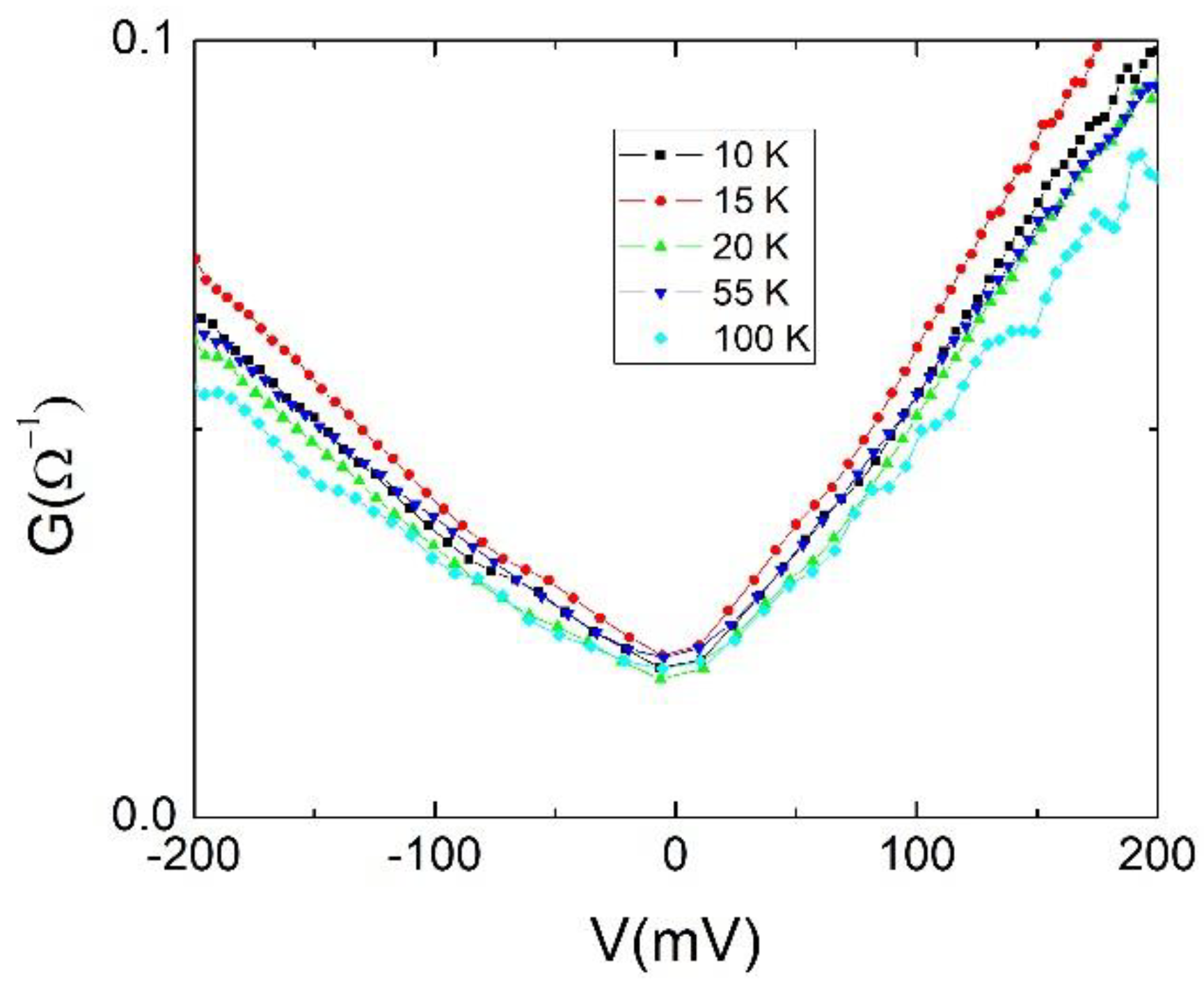
In some cases, a well definite V-shape is observed, as shown in Figure 11.
A linear differerential conductance has been often observed for HTCS based junctions with a larger slope for tunnelling along the c-axis [79]. A similar behavior has been reported into directional in-plane tunnelling PCS performed on single crystals of optimally doped Nd1.85Ce0.15CuO4-y, by driving a Au tip toward the cristal along [100] and [110] direction [15,28].
Considering the polycrystalline nature of our sample and the anisotropic properties of NCCO compound, the different slopes of the background conductance could be related to different tunnelling directions with respect to the orientation of the crystalline grains that may contribute to the overall shape of the conductance.
The linear background can be caused from an intrinsic mechanism like density of states effects [40] as well as from inelastic tunnelling from a broad distribution of scattering states as a result of non-stoichiometric oxygen in natural barrier of HTCS based junctions [80].
On the other hand, in addition to direct tunnelling, even localized states can contribute to the conductance, for instance coming from impurity and/or imperfections. In this case, a Fano resonance may provide an asymmetry in the conductance, like that observed in our high-bias data [61].
In conclusion PCS has been performed on bulk samples of electron-doped high temperature superconductor NCCO. The samples were characterized by a SEM equipped with a WDS for compositional measurements and with an EBSD detector for the analysis of grain orientation distribution. X-ray diffraction technique has also been used for structural characterization. Junctions in the tunnelling regime have been obtained with a gap feature at about 5 meV and no a zero-bias conductance peak has been observed. The conductance curves have been compared with the BTK model for a d-wave order parameter. The results could be indicative of a dominant current along the antinodal direction of the sample in case of order parameter with nodes or of a weakly angle dependence of the gap function. The high bias conductances have also been measured and a linear background has been often observed, indicative of intrinsic or extrinsic mechanisms.
Author Contributions
Conceptualization, P.R. and A.N.; methodology, P.R. and A.N.; software, F.A. and A.G.; investigation, F.A., A.G.; data curation, A.N., A. G., A.L., G.G.; writing—original draft preparation, P.R.; writing—review and editing, P.R. and A.N.; supervision, P.R.; All authors have read and agreed to the published version of the manuscript.
Funding
This research received no external funding.
Conflicts of Interest
The authors declare no conflict of interest.
References
- Huang, Qiang; Zasadzinski, J. F.; Gray, K. E. Phonon spectroscopy of superconducting Nb using point-contact tunneling. Phys. Rev. B 1990, 42, 7953. [CrossRef]
- DeWilde, Y., Miyakawa, N.; Guptasarma, P.; Iavarone, M.; Ozyuzer, L.; Zasadzinski, J. F.; Romano, P.; Hinks, D. G.; Kendziora, C.; Crabtree, G. W.; Gray, K. E. Unusual Strong-Coupling Effects in the Tunneling Spectroscopy of Optimally Doped and Overdoped Bi2Sr2CaCu2O8+δ. Phys. Rev. Lett. 1998, 80, 153-156. [CrossRef]
- Shan, L.; Wang, Y.; Zhu, X.; Mu, G.; Fang, L.; Ren, C.; Wen, H-H. Point-contact spectroscopy of iron-based layered superconductor LaO0.9F0.1−δFeAs. Europhysics Letters 2008, 83, 57004. [CrossRef]
- Szabó, P.; Samuely, P.; Kačmarčík, J.; Klein, T.; Marcus, J.; Fruchart, D.; Miraglia, S.; Marcenat, C.; Jansen, A.G.M. Evidence for Two Superconducting Energy Gaps in MgB2 by Point-Contact Spectroscopy. Phys. Rev. Lett. 2001, 87, 137005. [Google Scholar] [CrossRef] [PubMed]
- Giubileo, F.; Romeo, F.; Citro, R.; Di Bartolomeo, A.; Attanasio, C.; Cirillo, C.; Polcari, A.; Romano, P. Point contact Andreev reflection spectroscopy on ferromagnet/superconductor bilayers. Physica C: Superconductivity and its Applications, 2014, 503, 158–161. [Google Scholar] [CrossRef]
- Giubileo, F.; Romeo, F.; Di Bartolomeo, A.; Mizuguchi, Y.; Romano, P. Probing unconventional pairing in LaO0.5F0.5BiS2 layered superconductor by point contact spectroscopy. Journal of Physics and Chemistry of Solids 2018, 118, 192–199. [Google Scholar] [CrossRef]
- Wolf, E.L. Principles of Electron Tunneling Spectroscopy; 2nd ed.; Oxford University Press: Oxford, 2011.
- Fournier, P. T’ and infinite-layer electron-doped cuprates. Physica C 2015, 514, 314–338. [Google Scholar] [CrossRef]
- Armitage, N.P.; Fournier, P.; Greene, R.L. Progress and perspectives on electron-doped cuprates. Rev. Mod. Phys. 2010, 82, 2421–2487. [Google Scholar] [CrossRef]
- Song, D.; Han, G.; Kyung, W.; Seo, J.; Cho, C.; Kim, B.S.; Arita, M.; Shimada, K.; Namatame, H.; Taniguchi, M.; Yoshida, Y.; Eisaki, H.; Park, S.R.; Kim, C. Electron Number-Based Phase Diagram of Pr1−xLaCexCuO4−δ and Possible Absence of Disparity between Electron- and Hole-Doped Cuprate Phase Diagrams. Phys. Rev. Lett. 2017, 118, 137001. [Google Scholar] [CrossRef]
- Helm, T.; Kartsovnik, M. V.; Proust, C.; Vignolle, B.; Putzke, C.; Kampert, E.; Sheikin, I.; Choi, E.-S.; Brooks, J. S.; Bittner, N.; Biberacher, W.; Erb, A.; Wosnitza, J.; Gross, R. Correlation between Fermi surface transformations and superconductivity in the electron-doped high-Tc superconductor Nd2−xCexCuO4. Phys. Rev. B 2015, 92, 094501. [Google Scholar] [CrossRef]
- Armitage, N.P.; Lu, D.H.; Feng, D.L.; Kim, C.; Damascelli, A.; Shen, K.M.; Ronning, F.; Shen, Z.-X.; Onose, Y.; Taguchi, Y.; Tokura, Y. Superconducting gap anisotropy in Nd1.85Ce0.15CuO4: results from photoemission. Phys. Rev. Lett. 2001, 86, 1126–1129. [Google Scholar] [CrossRef]
- Sato, T.; Kamiyama, T.; Takahashi, T.; Kurahashi, K.; Yamada, K. Observation of dx2-y2-like superconducting gap in an electron-doped high-temperature superconductor. Science 2001, 291, 1517–1519. [Google Scholar] [CrossRef]
- Matsui, H.; Terashima, K.; Sato, T.; Takahashi, T.; Fujita, M.; Yamada, K. Direct observation of a nonmonotonic dx2-y2-wave superconducting gap in the electron-doped high-Tc superconductor Pr0:89LaCe0:11CuO4. Phys. Rev. Lett. 2005, 95, 017003. [Google Scholar] [CrossRef]
- Shan, L.; Huang, Y.; Wang, Y.L.; Li, S.; Zhao, J.; Dai, P.; Zhang, Y.Z.; Ren, C.; Wen, H.H. Weak-coupling Bardeen-Cooper-Schrieffer superconductivity in the electron doped cuprate superconductors, Phys. Rev. B 2008, 77, 014526. [CrossRef]
- Kokales, J.D.; Fournier, P.; Mercaldo, L.V.; Talanov, V.V.; Greene, R.L.; Anlage, S.M. Microwave electrodynamics of electron-doped cuprate superconductors. Phys. Rev. Lett. 2000, 85, 3696. [Google Scholar] [CrossRef]
- Prozorov, R.; Giannetta, R.; Fournier, P.; Greene, R.L. Evidence for nodal quasiparticles in electron-doped cuprates from penetration depth measurements. Phys. Rev. Lett. 2000, 85, 3700. [Google Scholar] [CrossRef]
- Snezhko, A.; Prozorov, R.; Lawrie, D.D.; Giannetta, R.; Gauthier, J.; Renaud, J.; Fournier, P. Nodal order parameter in electron-doped Pr2-xCexCuO4-d superconducting films. Phys. Rev. Lett. 2004, 92, 157005. [Google Scholar] [CrossRef]
- Blumberg, G.; Koitzsch, A.; Gozar, A.; Dennis, B.S.; Kendziora, C.A.; Fournier, P.; Greene, R.L. Nonmonotonic dx2_y2 superconducting order parameter in Nd2-xCexCuO4. Phys. Rev. Lett. 2002, 88, 107002. [Google Scholar] [CrossRef]
- Tsuei, C.C.; Kirtley, J.R. Phase-sensitive evidence for d-wave pairing symmetry in electron-doped cuprate superconductors, Phys. Rev. Lett. 2000, 85, 182–185. [Google Scholar] [CrossRef]
- Chesca, B.; Ehrhardt, K.; Mossle, M.; Straub, R.; Koelle, D.; Kleiner, R,; Tsukada, A. Magnetic-field dependence of the maximum supercurrent of La2-xCexCuO4-y interferometers: evidence for a predominant dx2-y2 superconducting order parameter. Phys. Rev. Lett. 2003, 90, 057004. [CrossRef]
- Ariando, D.; Darminto, H.J.H.; Smilde, V.; Leca, D.H.A.; Blank, H.; Rogalla, H.; Hilgenkamp, H. Phase-sensitive order parameter symmetry test experiments utilizing Nd2-xCexCuO4-y/Nb zigzag junctions. Phys. Rev. Lett. 2005, 94, 167001. [Google Scholar] [CrossRef]
- Armitage, N.P.; Ronning, F.; Lu, D.H.; Kim, C.; Damascelli, A.; Shen, K.M.; Feng, D.L.; Eisaki, H.; Shen, Z.-X.; Mang, P.K.; Kaneko, N.; Greven, M.; Onose, Y.; Taguchi, Y.; Tokura, Y. Doping dependence of an n-type cuprate superconductor investigated by angle-resolved photoemission spectroscopy. Phys. Rev. Lett. 2002, 88, 257001. [Google Scholar] [CrossRef]
- Dagan, Y., and Greene, R. L. Hole superconductivity in the electron-doped superconductor Pr2−xCexCuO4. Phys. Rev. B 2007, 76, 024506. [CrossRef]
- Yuan, Qingshan; Chen, Yan; Lee, T. K.; Ting, C. S. Fermi surface evolution in the antiferromagnetic state for the electron-doped t−t′−t′′−J model. Phys. Rev. B 2004, 69, 214523. [CrossRef]
- Luo H. G.; and Xiang; T. Superfluid Response in Electron-Doped Cuprate Superconductors. Phys. Rev. Lett. 2005, 94, 027001. [CrossRef]
- Liu, C. S.; Luo, H. G.; Wu, W. C.; and Xiang, T. Two-band model of Raman scattering on electron-doped high-Tc superconductors. Phys. Rev. B 2006, 73, 174517. [Google Scholar] [CrossRef]
- Shan, L.; Huang, Y.; Gao, H.; Wang, Y.; Li, S. L.; Dai, P. C.; Zhou, F.; Xiong, J. W.; Ti, W. X.; and Wen, H. H. Distinct pairing symmetries in Nd1.85Ce0.15CuO4−y and La1.89Sr0.11CuO4 single crystals: Evidence from comparative tunneling measurements. Phys. Rev. B, 2005, 72, 144506. [Google Scholar] [CrossRef]
- Li, Y.; Tabis, W.; Tang, Y.; Yu, G.; Jaroszynski, J.; Barišić, N.; and Greven, M. Hole pocket-driven superconductivity and its universal features in the electron-doped cuprates. Sci. Adv. 2019, 5, eaap7349. [Google Scholar] [CrossRef]
- Hirsch J., and Marsiglio, F. Understanding electron-doped cuprate superconductors as hole superconductors. Physica C 2019, 564, 29. [CrossRef]
- Qazilbash, M. M.; Koitzsch, A.; Dennis, B. S.; Gozar, A.; Balci, Hamza; Kendziora, C. A.; Greene, R. L.; Blumberg, G. Evolution of superconductivity in electron-doped cuprates: Magneto-Raman spectroscopy. Phy.Rev.B. 2005, 72, 214510. [CrossRef]
- Armitage N. P. et al. Anomalous Electronic Structure and Pseudogap Effects in Nd1.85Ce0.15CuO4. Phys. Rev. Lett. 2001, 87, 147003. [CrossRef]
- Yamashiro, M.; Tanaka, Y.; Tanuma, Y.; Kashiwaya, S. Theory of tunneling conductance for normal metal/insulator/triplet superconductor junction. J. Phys. Soc. Jpn. 1998, 67, 3224. [Google Scholar] [CrossRef]
- Mourachkine, A. Andreev reflections and tunneling spectroscopy on underdoped Nd1.85Ce0.15CuO4–δ. Europhys. Lett. 2000, 50, 663. [Google Scholar] [CrossRef]
- Biswas, Amlan; Fournier, P.; Qazilbash, M. M.; Smolyaninova, V. N.; Balci, Hamza; Greene, R. L. Evidence of a d- to s-Wave Pairing Symmetry Transition in the Electron-Doped Cuprate Superconductor Pr2−xCexCuO4. Phys. Rev. Lett. 2002, 88, 207004. [CrossRef]
- Liu, C.S. and Wu, W.C. Theory of point-contact spectroscopy in electron-doped cuprate superconductors. Phys. Rev. B 2007, 76, 220504. [CrossRef]
- Kim, M.-S.; Skinta, J.A.; Lemberger, T.R.; Tsukada, A.; Naito, M. Evidence for a Transition in the Pairing Symmetry of the Electron-Doped Cuprates La2−xCexCuO4−y and Pr2−xCexCuO4−y. Phys. Rev. Lett. 2003, 91, 087001. [Google Scholar] [CrossRef]
- Skinta, J.A.; Kim, M.-S.; Lemberger, T.R.; Greibe, T.; Naito, M. Evidence for a Transition in the Pairing Symmetry of the Electron-Doped Cuprates. Phys. Rev. Lett. 2002, 88, 207005. [Google Scholar] [CrossRef]
- Zimmers, A.; Lobo, R. P. S. M.; Bontemps, N.; Homes, C. C.; Barr, M. C.; Dagan, Y.; Greene, R. L. Infrared signature of the superconducting state in Pr2−xCexCuO4. Phys. Rev.B 2004, 70, 132502. [Google Scholar] [CrossRef]
- Cucolo, A. M.; Di Leo, R.; Nigro, A.; Romano, P.; and Bobba, F. Linear normal conductance in copper oxide tunnel junctions. Phys. Rev. B 1996, 54, R9686–R9688. [Google Scholar] [CrossRef]
- Naito, M.; Krockenberger, Y.; Ikeda, A.; Yamamoto, H. Reassessment of the electronic state, magnetism, and superconductivity in high-Tc cuprates with the Nd2CuO4 structure. Physica C 2016, 523, 28. [Google Scholar] [CrossRef]
- Radaelli, P. G.; Jorgensen, J. D.; Schultz, A. J.; Peng, J. L.; Greene, R. L. Evidence of apical oxygen in Nd2CuOy determined by single-crystal neutron diffraction. Phys. Rev. B 1994, 49, 15322. [Google Scholar] [CrossRef]
- Mang, P. K.; Larochelle, S.; Mehta, A.; Vajk, O. P.; Erickson, A. S.; Lu, L.; Buyers, W. J. L.; Marshall, A. F.; Prokes, K.; Greven, M. Phase decomposition and chemical inhomogeneity in Nd2−xCexCuO4±δ. Phys. Rev. B 2004, 70, 094507. [Google Scholar] [CrossRef]
- Xu, X. Q.; Mao, S. N.; Jiang, W.; Peng, J. L.; Greene, R. L. Oxygen dependence of the transport properties of Nd1.78Ce0.22CuO4±δ. Phys. Rev. B 1996, 53, 871. [Google Scholar] [CrossRef]
- Higgins, J. S.; Dagan, Y.; Barr, M. C.; Weaver, B. D.; Greene, R. L. Role of oxygen in the electron-doped superconducting cuprates. Phys. Rev. B 2006, 73, 104510. [Google Scholar] [CrossRef]
- Riou, G.; Richard, P.; Jandl, S.; Poirier, M.; Fournier, P.; Nekvasil, V.; Barilo, S. N.; Kurnevich, L. A. Pr3+ crystal-field excitation study of apical oxygen and reduction processes in Pr2−xCexCuO4±δ. Phys. Rev. B 2004, 69, 024511. [Google Scholar] [CrossRef]
- Richard, P.; Riou, G.; Hetel, I.; Jandl, S.; Poirier, M.; Fournier, P. Role of oxygen nonstoichiometry and the reduction process on the local structure of Nd2−xCexCuO4±δ. Phys. Rev. B 2004, 70, 064513. [Google Scholar] [CrossRef]
- Kang, H. J.; Dai, P.; Campbell, B. J.; Chupas, P. J.; Rosenkranz, S.; Lee, P. L.; Huang, Q.; Li, S.; Komiya, S.; Ando, Y. Microscopic annealing process and its impact on superconductivity in T’-structure electron-doped copper oxides. Nat. Mater. 2007, 6, 224. [Google Scholar] [CrossRef]
- Romano, P.; Riccio, M.; Guarino, A.; Martucciello, N.; Grimaldi, G.; Leo, A.; Nigro, A. Electron doped superconducting cuprates for photon detectors. Measurement 2018, 122, 502–506. [Google Scholar] [CrossRef]
- Guarino, A.; Autieri, C.; Marra, P.; Leo, A.; Grimaldi, G.; Avella, A.; and Nigro, A. Superconductivity induced by structural reorganization in the electron-doped cuprate Nd2−xCexCuO4. Phys. Rev. B 2022, 105, 014512. [Google Scholar] [CrossRef]
- Guarino, A.; Fittipaldi, R.; Romano, A.; Vecchione, A.; Nigro, A. Correlation between structural and transport properties in epitaxial films of Nd2−xCexCuO4±δ. Thin Solid Films 2012, 524, 282. [Google Scholar] [CrossRef]
- Guarino, A.; Leo, A.; Avella, A.; Avitabile, F.; Martucciello, N.; Grimaldi, G.; Romano, A.; Pace, S.; Romano, P.; Nigro, A. Electrical transport properties of sputtered Nd2−xCexCuO4±δ thin films. Physica B 2018, 536, 742–746. [Google Scholar] [CrossRef]
- Guarino, A.; Patimo, G.; Vecchione, A.; Di Luccio, T.; Nigro, A. Fabrication of superconducting Nd2−xCexCuO4±δ films by automated dc sputtering technique. Physica C 2013, 495, 146. [Google Scholar] [CrossRef]
- Guarino, A.; Leo, A.; Grimaldi, G.; Martucciello, N.; Dean, C.; Kunchur, M. N.; Pace, S.; Nigro, A. Pinning mechanism in electron-doped HTS Nd1.85Ce0.15CuO4−δ epitaxial films. Supercond. Sci. Technol. 2014, 27, 124011. [Google Scholar] [CrossRef]
- Avella, A.; Buonavolontà, C.; Guarino, A.; Valentino, M.; Leo, A.; Grimaldi, G.; de Lisio, C.; Nigro, A.; Pepe, G. Disorder-sensitive pump-probe measurements on Nd1.83Ce0.17CuO4±δ films. Phys. Rev. B 2016, 94, 115426. [Google Scholar] [CrossRef]
- Guarino, A.; Romano, P.; Avitabile, F.; Leo, A.; Martucciello, N.; Grimaldi, G.; Ubaldini, A.; D’Agostino, D.; Bobba, F.; Vecchione, A.; Pace, S.; Nigro, A. Characterization of Nd2−xCexCuO4±δ (x = 0 and 0.15) Ultrathin Films Grown by DC Sputtering Technique. IEEE Trans. Appl. Supercond. 2017, 27, 1-4. [CrossRef]
- Uthayakumar, S.; Fittipaldi, R.; Guarino, A.; Vecchione, A.; Romano, A.; Nigro, A.; Habermeier, H.-U.; Pace, S. Thermal treatments and evolution of bulk Nd1.85Ce0.15CuO4 morphology, Physica C 2008, 468, 2271-2274. [CrossRef]
- Andreev, A.F. The Thermal Conductivity of the Intermediate State in Superconductors. J. Exp. Theor. Phys. 1964, 19, 1228. [Google Scholar]
- Deutscher, G. Andreev–Saint-James reflections: A probe of cuprate superconductors. Rev. Mod. Phys. 2005, 77, 109–135. [Google Scholar] [CrossRef]
- Bardeen, J.; Cooper, L. N.; and Schrieffer, J. R. Theory of Superconductivity. Phys. Rev. 1957, 108, 1175–1204. [Google Scholar] [CrossRef]
- Blonder, G.E.; Tinkham, M.; Klapwijk, T.M. Transition from metallic to tunneling regimes in superconducting microconstrictions: Excess current, charge imbalance, and supercurrent conversion. Phys. Rev. B 1982, 25, 4515–4532. [Google Scholar] [CrossRef]
- Fano, U. Effects of Configuration Interaction on Intensities and Phase Shifts. PhysRev. 1961, 124, 1866–1878. [Google Scholar] [CrossRef]
- Huang, Q.; Zasadzinski, J.; Tralshawala, N. et al. Tunnelling evidence for predominantly electron–phonon coupling in superconducting Ba1−xKxBiO3 and Nd2−xCexCuO4−y. Nature 1990, 347, 369–372. [CrossRef]
- Blumberg, G.; Koitzsch, A.; Gozar, A.; Dennis, B. S.; Kendziora, C. A.; Fournier, P.; Greene, R. L. Nonmonotonic dx2−y2 Superconducting Order Parameter in Nd2−xCexCuO4. Phys. Rev. Lett. 2002, 88, 107002. [Google Scholar] [CrossRef]
- Kashiwaya, S.; Matsubara, N.; Prijamboedi, B. et al. Doping Dependence of Superconducting Energy Gap of NCCO Observed by Tunnelling Spectroscopy. J. Low Temp. Phys. 2003, 131, 327–330. [CrossRef]
- Wang, Y.; Perdew, J.P. Spin scaling of the electron-gas correlation energy in the high-density limit. Phys.Rev.B 1991, 43, 8911–8916. [Google Scholar] [CrossRef]
- Onose, Y.; Taguchi, Y.; Ishizaka, K.; Tokura, Y. Charge dynamics in underdoped Nd2−xCexCuO4: Pseudogap and related phenomena. Phys. Rev. B 2004, 69, 024504. [Google Scholar] [CrossRef]
- Lee, P.A.; Ramakrishnan, T. V. Disordered electronic systems. Rev. Mod. Phys. 1985, 57, 287–337. [Google Scholar] [CrossRef]
- Duif, A.M.; Jansen, A.G.M.; Wyder, P. Point-contact spectroscopy. J. Phys. Condens. Matter 1989, 1, 3157–3189. [Google Scholar] [CrossRef]
- Dynes, R. C.; Narayanamurti, V.; Garno, J. P. Direct Measurement of Quasiparticle-Lifetime Broadening in a Strong-Coupled Superconductor. Phys.Rev.Lett. 1978, 41, 1509–1512. [Google Scholar] [CrossRef]
- Pleceník, A.; Grajcar, M.; Beňačka, Š.; Seidel, P.; Pfuch, A. Finite-quasiparticle-lifetime effects in the differential conductance of Bi2Sr2CaCu2Oy/Au junctions. Phys. Rev. B 1994, 49, 10016–10019. [Google Scholar] [CrossRef]
- Shan, L.; Huang, Y.; Ren, C.; Wen, H. H. Vortex overlapping in a BCS type-II superconductor revealed by Andreev reflection spectroscopy. Phys. Rev. B 2006, 73, 134508. [Google Scholar] [CrossRef]
- Dagan, Y.; Qazilbash, M. M.; Greene, R. L. Tunneling into the Normal State of Pr2−xCexCuO4. Phys. Rev. Lett. 2005, 94, 187003. [Google Scholar] [CrossRef]
- Dagan, Y.; Beck, R.; Greene, R. L. Dirty Superconductivity in the Electron-Doped Cuprate Pr2−xCexCuO4−δ: Tunneling Study. Phys. Rev. Lett. 2007, 99, 147004. [Google Scholar] [CrossRef]
- Matsui, H.; Terashima, K.; Sato, T.; Takahashi, T.; Fujita, M.; Yamada, K. Direct Observation of a Nonmonotonic dx2−y2-Wave Superconducting Gap in the Electron-Doped High-Tc Superconductor Pr0.89LaCe0.11CuO4. Phys. Rev. Lett. 2005, 95, 017003. [Google Scholar] [CrossRef]
- Liu, C. S. and Wu, W. C. Theory of point-contact spectroscopy in electron-doped cuprate superconductors. Phys. Rev. B 2007, 76, 220504. [CrossRef]
- Simmons, J.G. Electric Tunnel Effect between Dissimilar Electrodes Separated by a Thin Insulating Film. J.Appl.Phys. 1963, 34, 2581–2590. [Google Scholar] [CrossRef]
- Brinkman, W. F.; Dynes, R. C.; Rowell, J. M. Tunneling Conductance of Asymmetrical Barriers. J. Appl. Phys. 1970, 41, 1915–1921. [Google Scholar] [CrossRef]
- Guarino, A.; Romano, P.; Fujii, J.; Ruosi, A.; Avitabile, F.; Vobornik, I.; Panaccione, G.; Vecchione, A.; Nigro, A. Study of the surface properties of NCCO electron-doped cuprate. Eur. Phys. J. Spec. Top. 2019, 228, 733–739. [Google Scholar] [CrossRef]
- Mandrus, D.; Forro, L.; Koller, D.; Mihaly, L. Giant tunnelling anisotropy in the high- Tc superconductor Bi2Sr2CaCu2O8. Nature 1991, 351, 460–462. [Google Scholar] [CrossRef]
- Kirtley, J. R.; Washburn, S.; Scalapino, D. J. Origin of the linear tunneling conductance background. Phys. Rev. B 1992, 45, 336–346. [Google Scholar] [CrossRef]
Figure 1.
Diffractogram of our NCCO sample after the reduction process. The inset shows the diffraction identifications panel by X’Pert Highscore software: the accepted pattern corresponds to the chart ICDD 01-080-1645 containing the crystallographic parameters of a bulk sample of Nd1.85Ce0.15CuO4.
Figure 1.
Diffractogram of our NCCO sample after the reduction process. The inset shows the diffraction identifications panel by X’Pert Highscore software: the accepted pattern corresponds to the chart ICDD 01-080-1645 containing the crystallographic parameters of a bulk sample of Nd1.85Ce0.15CuO4.
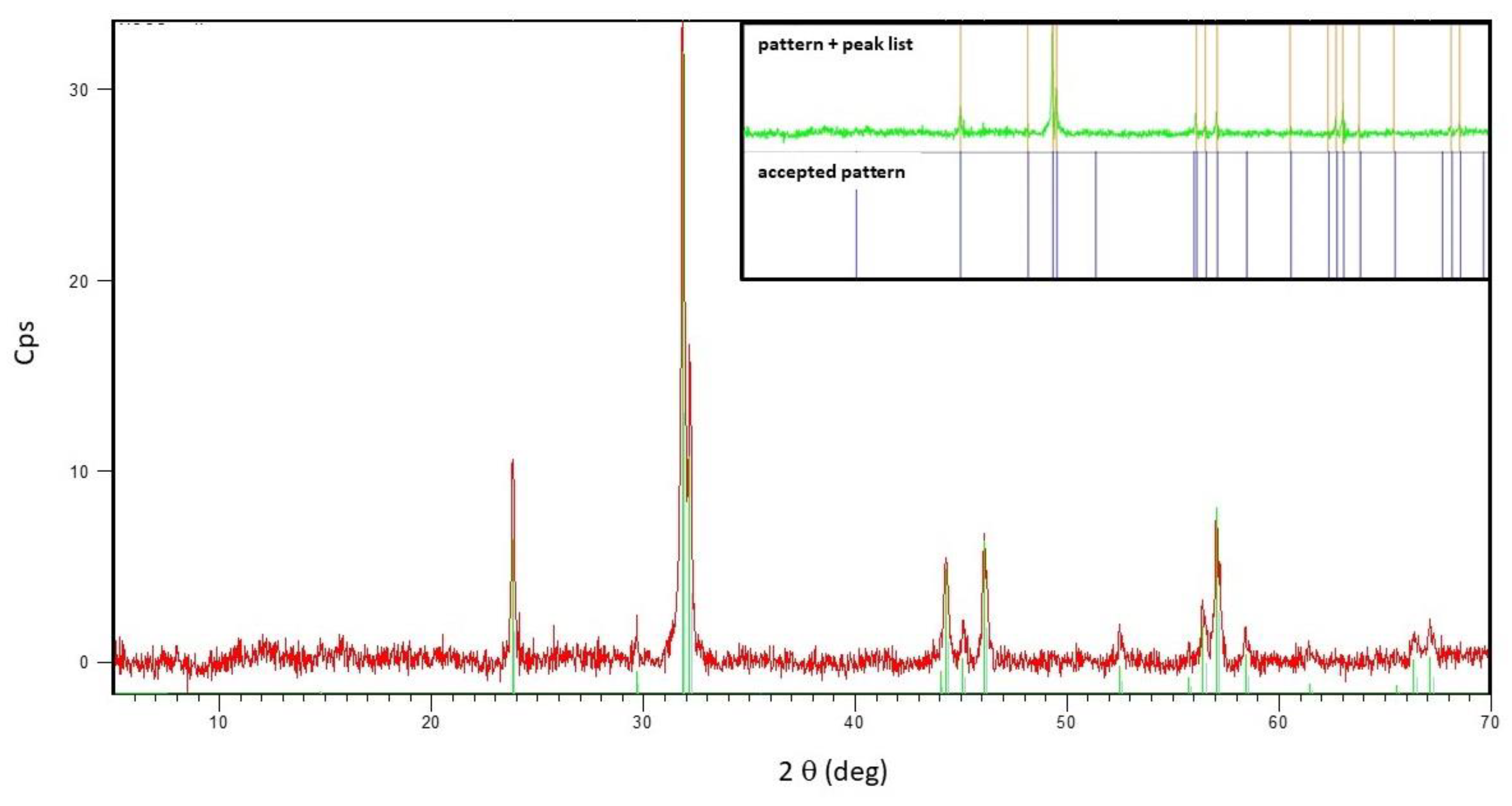
Figure 2.
WDS trace scan elements in the wavelength range 1.14–30 Å for a NCCO sample. In the inset a zoom in the range from 1.2 to 2.4 Å is reported. All the peaks are first or higher orders Bragg reflections of X-rays characteristic of Nd, Ce, Cu, and O.
Figure 2.
WDS trace scan elements in the wavelength range 1.14–30 Å for a NCCO sample. In the inset a zoom in the range from 1.2 to 2.4 Å is reported. All the peaks are first or higher orders Bragg reflections of X-rays characteristic of Nd, Ce, Cu, and O.
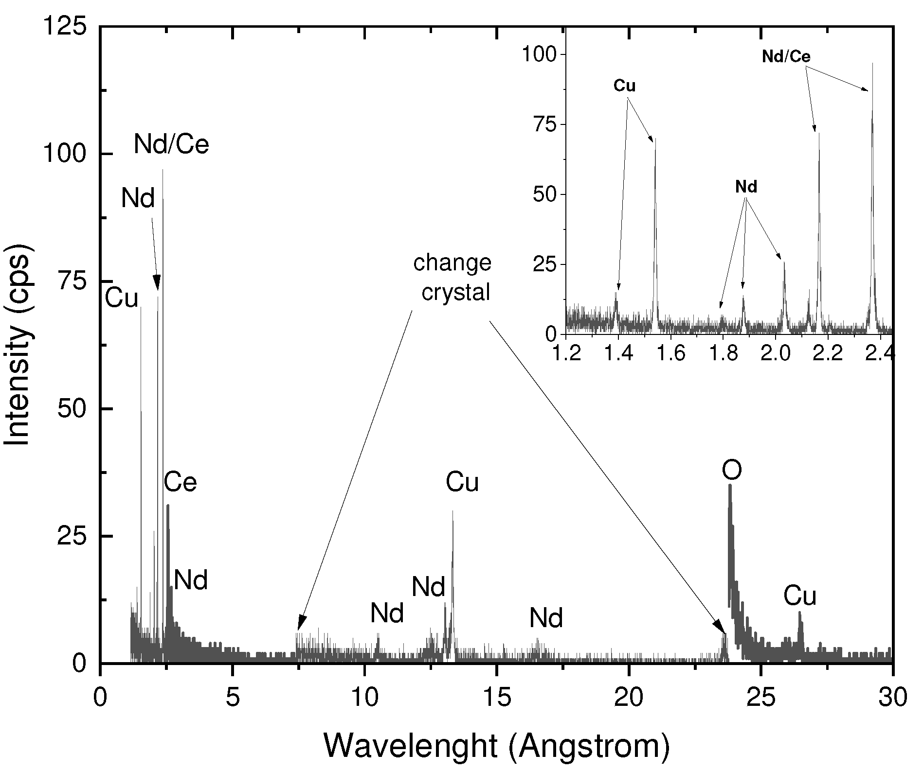
Figure 3.
SEM image of a NCCO sample is shown. SN, RD and TD represent the sample directions reference with respect to which the orientation of the crystal cells is reported. The inverse pole figures plotted with crystal directions as the axes of the figure, for each sample direction, denote the polycrystalline nature of the sample.
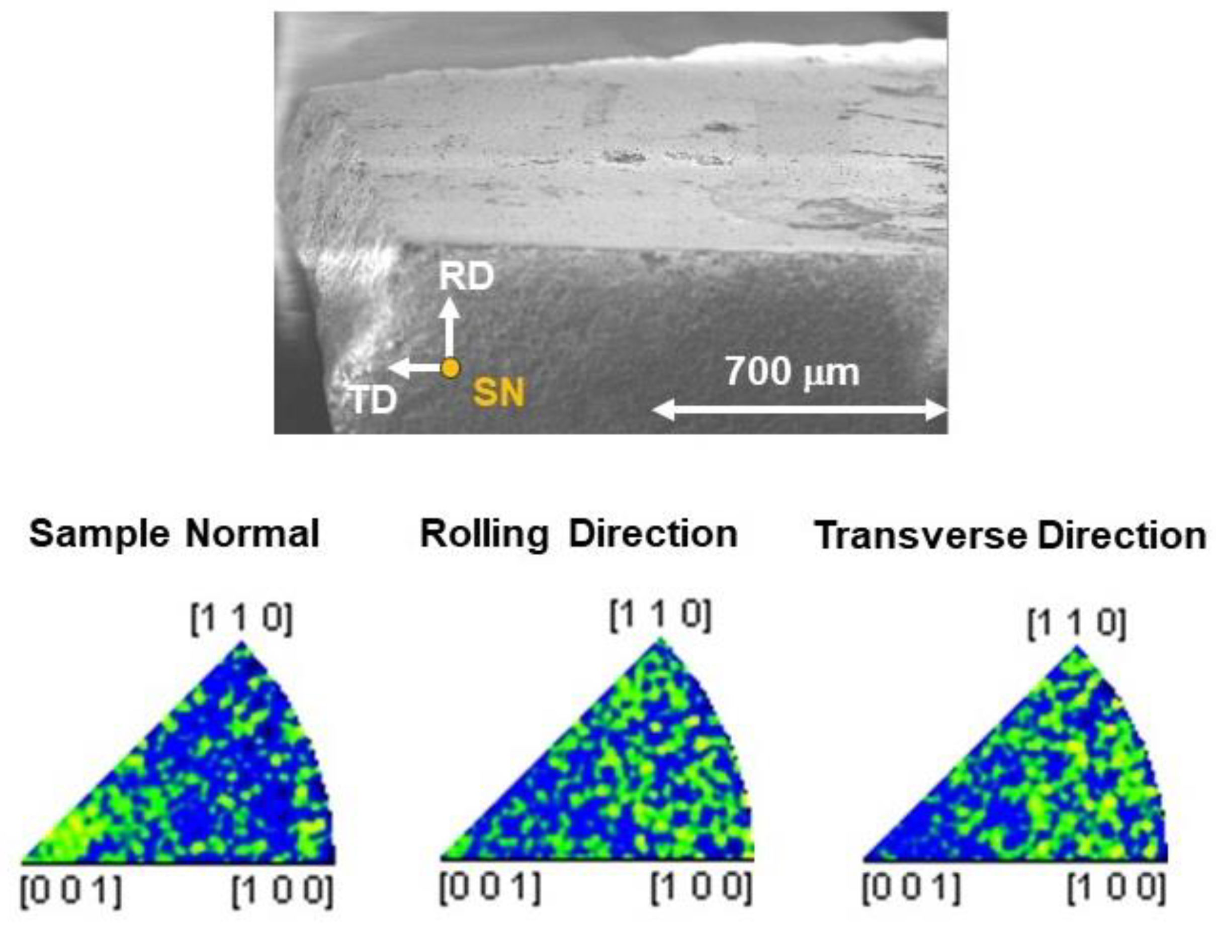
Figure 4.
On the left, SEM image of the sample with its superimposed orientation map. On the right, a grain size plot from which it follows that the majority of grains of this sample has dimensions of about 220 μm2.
Figure 4.
On the left, SEM image of the sample with its superimposed orientation map. On the right, a grain size plot from which it follows that the majority of grains of this sample has dimensions of about 220 μm2.
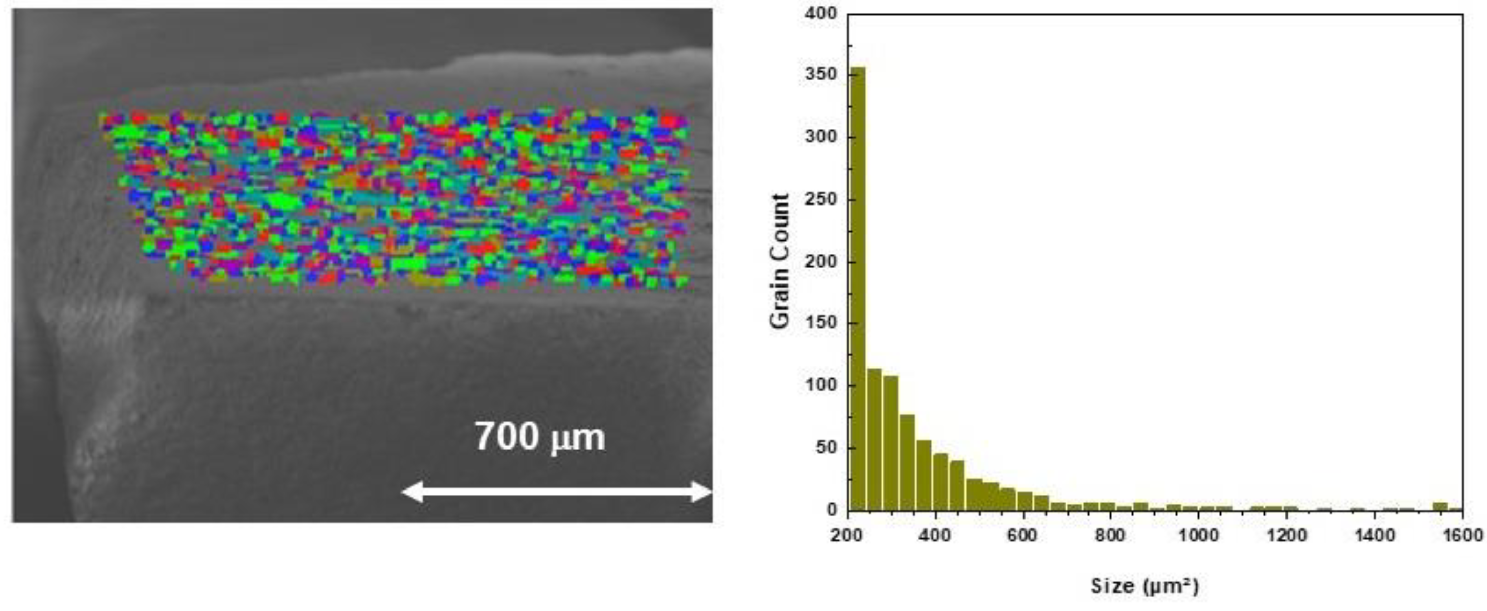
Figure 5.
On the left, grain map calculated with a misorientation angle threshold of 5° and superimposed on a SEM image at high magnification. On the right, changes of the misorientation angles for the different profile scans indicated in the grain map.
Figure 5.
On the left, grain map calculated with a misorientation angle threshold of 5° and superimposed on a SEM image at high magnification. On the right, changes of the misorientation angles for the different profile scans indicated in the grain map.
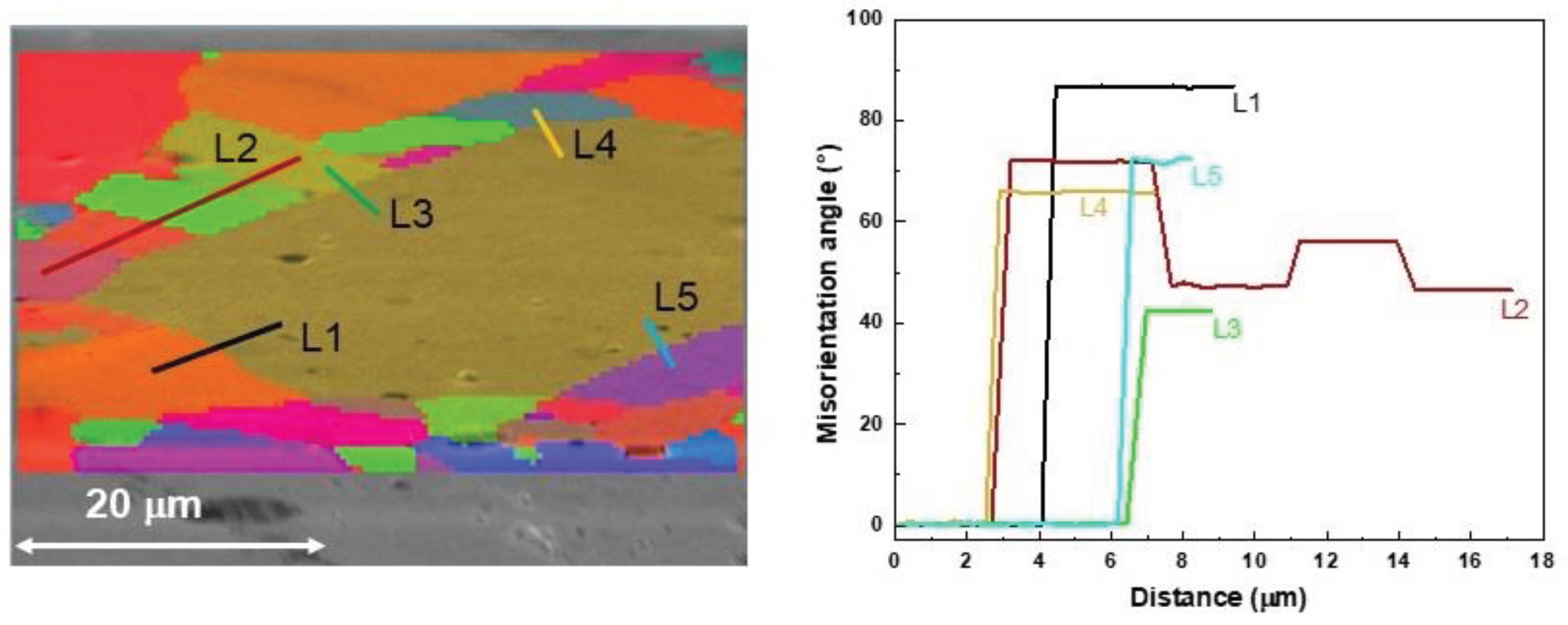
Figure 6.
a) orientation map along the normal direction of a sample and b) reference color key for the NCCO tetragonal crystalline structure. c) Distributions of the pixels with a certain color intensity selecting different channels.
Figure 6.
a) orientation map along the normal direction of a sample and b) reference color key for the NCCO tetragonal crystalline structure. c) Distributions of the pixels with a certain color intensity selecting different channels.
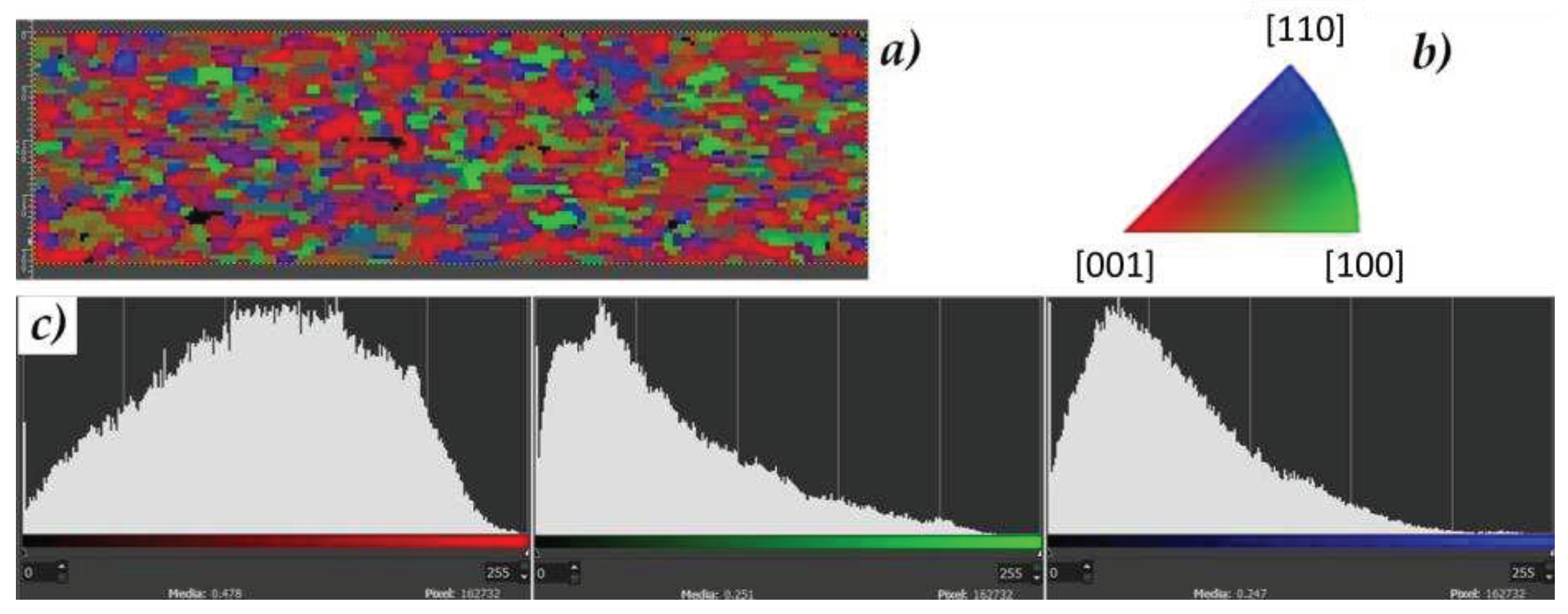
Figure 7.
Normalized conductance at T = 0 K and with Z = 5 in the case of isotropic s-wave symmetry a) and d-wave symmetry with bc) and d) .
Figure 7.
Normalized conductance at T = 0 K and with Z = 5 in the case of isotropic s-wave symmetry a) and d-wave symmetry with bc) and d) .
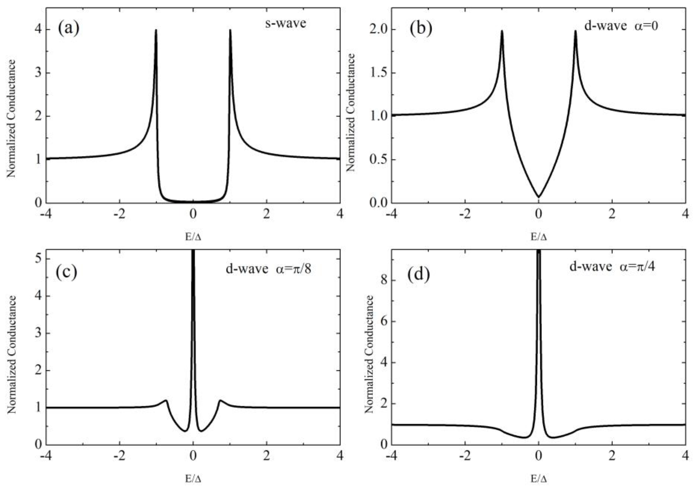
Figure 8.
Differential conductance for junctions with resistances a) 45 Ω and b) 150 Ω); Normalized conductance for the junctions of panel (a) and (b) compared with the BTK model for a d-wave order parameter, red solid line. (c) α = 0, Δ = 4.5 meV, Z = 2.2 and Γ=1.8 ; (d) α=0, Δ = 4.5 meV, Z=1.5 and Γ=3.2.
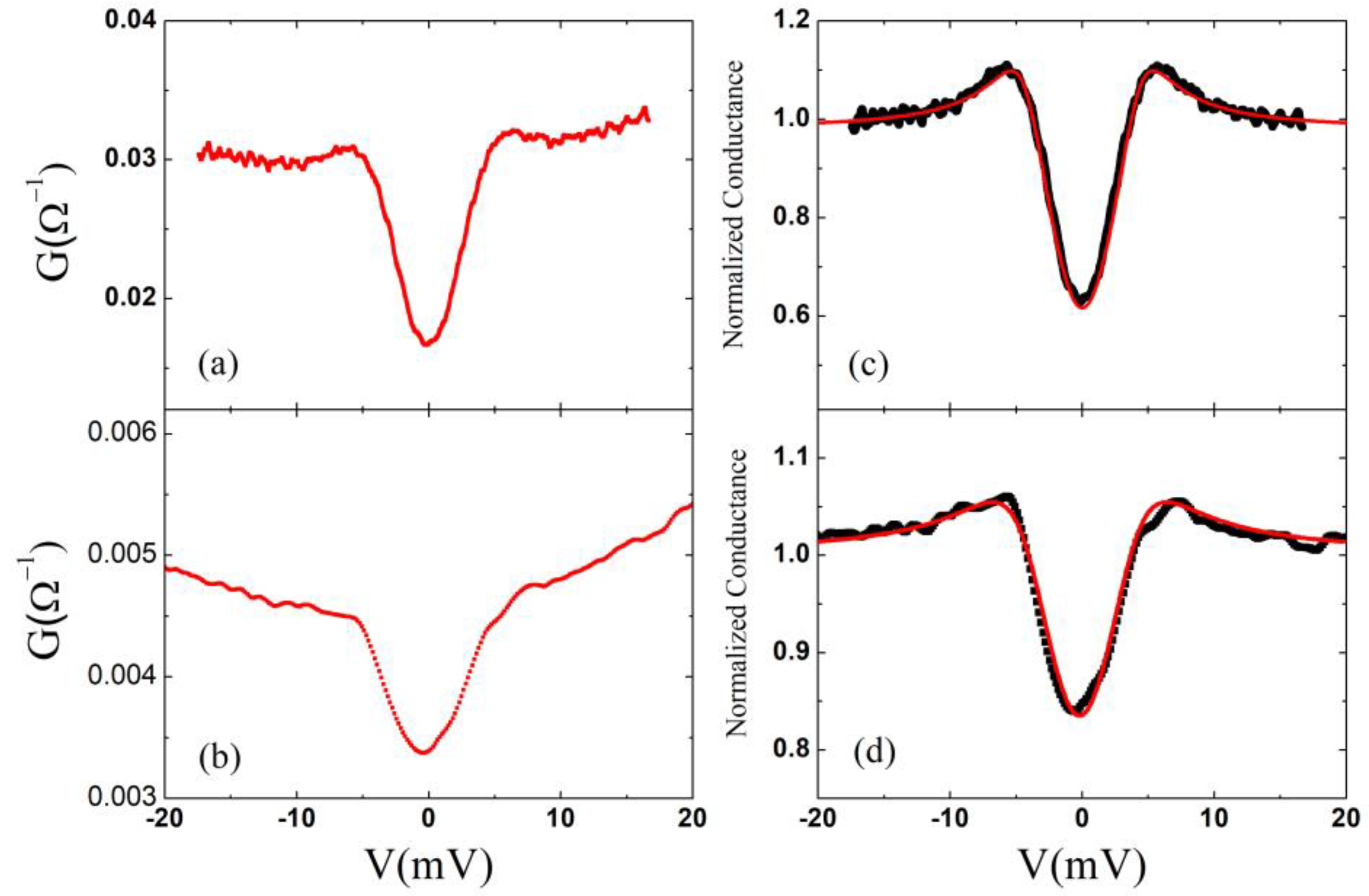
Figure 9.
Conductance temperature dependence for the 150Ω junction.
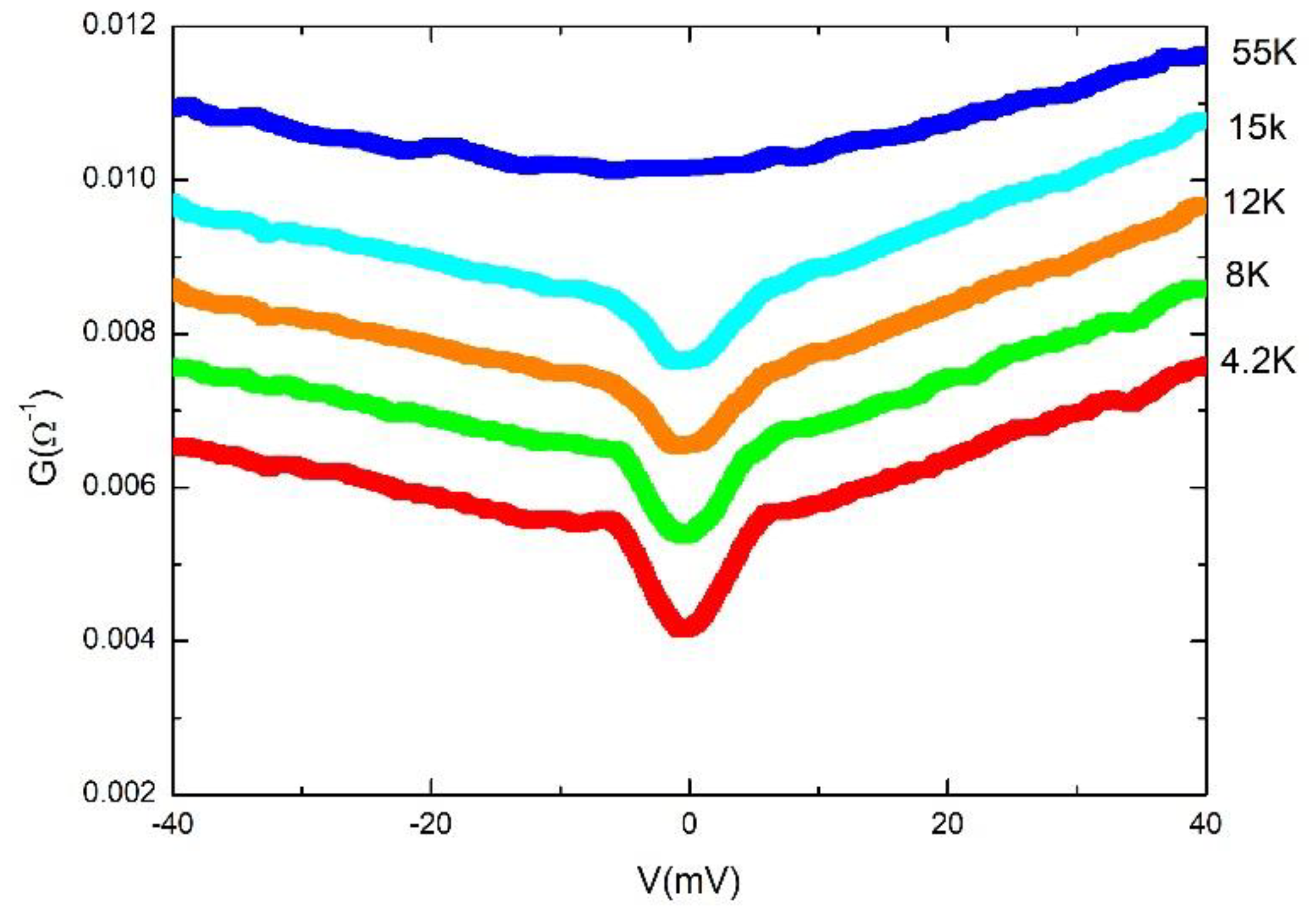
Figure 10.
High-bias conductance:parabolic background for 85Ω junction.
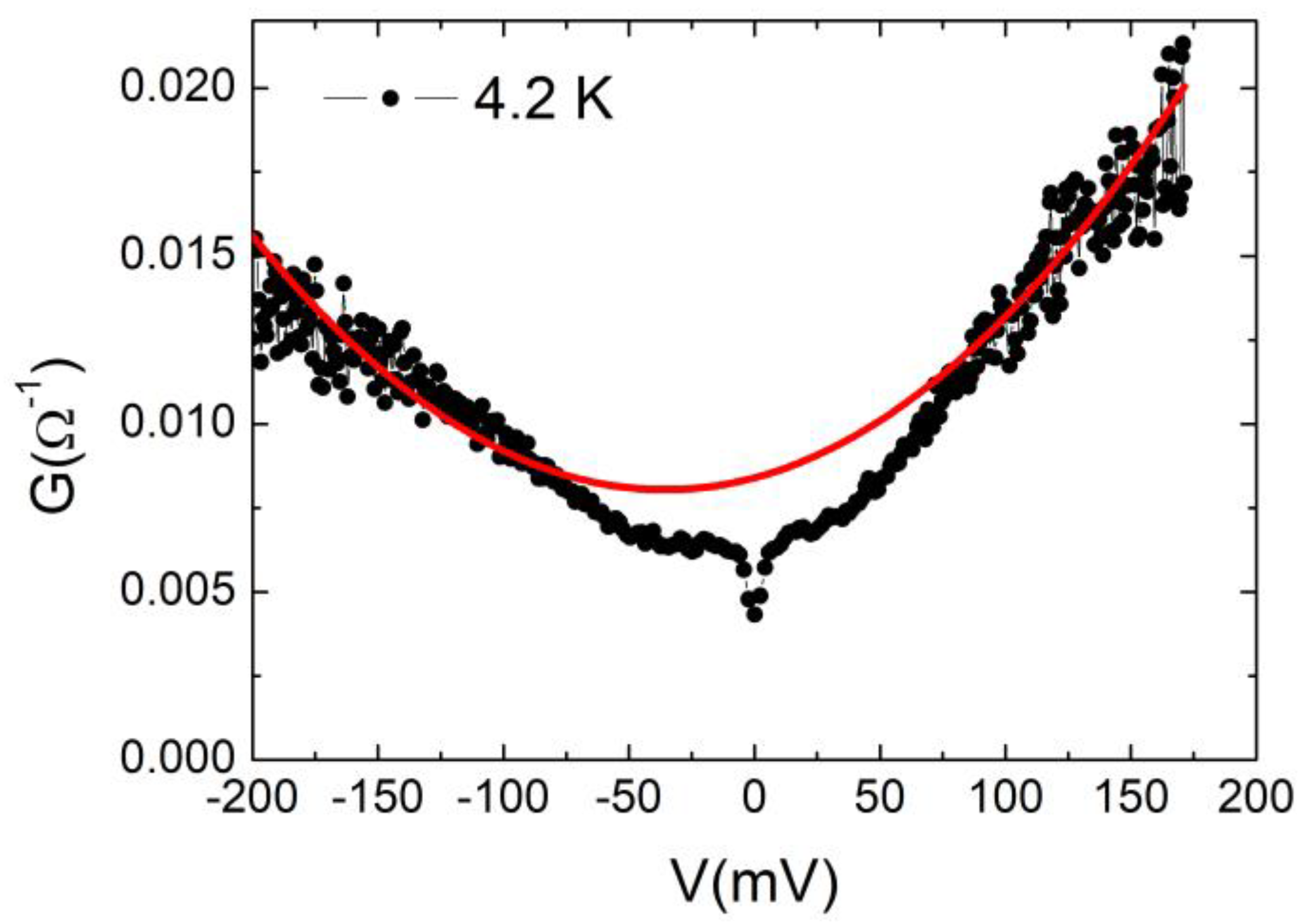
Figure 11.
High-bias conductance: linear background for 7.5 Ω junction.
Disclaimer/Publisher’s Note: The statements, opinions and data contained in all publications are solely those of the individual author(s) and contributor(s) and not of MDPI and/or the editor(s). MDPI and/or the editor(s) disclaim responsibility for any injury to people or property resulting from any ideas, methods, instructions or products referred to in the content. |
© 2023 by the authors. Licensee MDPI, Basel, Switzerland. This article is an open access article distributed under the terms and conditions of the Creative Commons Attribution (CC BY) license (http://creativecommons.org/licenses/by/4.0/).
Copyright: This open access article is published under a Creative Commons CC BY 4.0 license, which permit the free download, distribution, and reuse, provided that the author and preprint are cited in any reuse.


